US6560155B1 - System and method for power saving memory refresh for dynamic random access memory devices after an extended interval - Google Patents
System and method for power saving memory refresh for dynamic random access memory devices after an extended intervalDownload PDFInfo
- Publication number
- US6560155B1 US6560155B1US10/002,707US270701AUS6560155B1US 6560155 B1US6560155 B1US 6560155B1US 270701 AUS270701 AUS 270701AUS 6560155 B1US6560155 B1US 6560155B1
- Authority
- US
- United States
- Prior art keywords
- refresh
- row
- dram
- address signal
- row addressing
- Prior art date
- Legal status (The legal status is an assumption and is not a legal conclusion. Google has not performed a legal analysis and makes no representation as to the accuracy of the status listed.)
- Expired - Lifetime, expires
Links
- 230000015654memoryEffects0.000titleclaimsdescription344
- 238000000034methodMethods0.000titleclaimsdescription31
- 230000003111delayed effectEffects0.000claimsdescription28
- 230000004044responseEffects0.000claimsdescription15
- 230000000977initiatory effectEffects0.000claimsdescription11
- 239000004020conductorSubstances0.000claimsdescription8
- 238000010586diagramMethods0.000description13
- 239000003990capacitorSubstances0.000description10
- 239000000463materialSubstances0.000description6
- 230000008901benefitEffects0.000description5
- 238000003491arrayMethods0.000description4
- 230000001934delayEffects0.000description3
- 230000006870functionEffects0.000description3
- 230000015572biosynthetic processEffects0.000description2
- 230000008569processEffects0.000description2
- 230000009467reductionEffects0.000description2
- 230000001360synchronised effectEffects0.000description2
- 230000003213activating effectEffects0.000description1
- 230000004913activationEffects0.000description1
- 238000004364calculation methodMethods0.000description1
- 238000001816coolingMethods0.000description1
- 230000008878couplingEffects0.000description1
- 238000010168coupling processMethods0.000description1
- 238000005859coupling reactionMethods0.000description1
- 238000013500data storageMethods0.000description1
- 238000009792diffusion processMethods0.000description1
- 230000009977dual effectEffects0.000description1
- 230000000694effectsEffects0.000description1
- 238000005516engineering processMethods0.000description1
- 229910000078germaneInorganic materials0.000description1
- 239000011521glassSubstances0.000description1
- 230000020169heat generationEffects0.000description1
- 239000011810insulating materialSubstances0.000description1
- 230000007246mechanismEffects0.000description1
- 230000005055memory storageEffects0.000description1
- 239000002923metal particleSubstances0.000description1
- 230000005012migrationEffects0.000description1
- 238000013508migrationMethods0.000description1
- 230000002093peripheral effectEffects0.000description1
- 230000033764rhythmic processEffects0.000description1
- 239000004065semiconductorSubstances0.000description1
- 229910052709silverInorganic materials0.000description1
- 239000004332silverSubstances0.000description1
- 230000009466transformationEffects0.000description1
- 230000000007visual effectEffects0.000description1
- 239000002918waste heatSubstances0.000description1
Images


Classifications
- G—PHYSICS
- G11—INFORMATION STORAGE
- G11C—STATIC STORES
- G11C11/00—Digital stores characterised by the use of particular electric or magnetic storage elements; Storage elements therefor
- G11C11/21—Digital stores characterised by the use of particular electric or magnetic storage elements; Storage elements therefor using electric elements
- G11C11/34—Digital stores characterised by the use of particular electric or magnetic storage elements; Storage elements therefor using electric elements using semiconductor devices
- G11C11/40—Digital stores characterised by the use of particular electric or magnetic storage elements; Storage elements therefor using electric elements using semiconductor devices using transistors
- G11C11/401—Digital stores characterised by the use of particular electric or magnetic storage elements; Storage elements therefor using electric elements using semiconductor devices using transistors forming cells needing refreshing or charge regeneration, i.e. dynamic cells
- G11C11/406—Management or control of the refreshing or charge-regeneration cycles
Definitions
- the present inventionis directed to dynamic random access memory (DRAM) devices, and, more particularly, to a system and method for saving power while refreshing DRAM devices such as programmable conductor DRAM (PCDRAM) devices which only need to be refreshed after an extended interval.
- DRAMdynamic random access memory
- PCDRAMprogrammable conductor DRAM
- DRAMdynamic random access memory
- DRAM devicesare fairly inexpensive because a DRAM memory cell needs relatively few components to store a data bit as compared with other types of memory cells. Thus, a large system memory can be implemented using DRAM devices for a relatively low cost.
- DRAM deviceshave the disadvantage that their memory cells must be continually refreshed because of the inherently transitory nature of their storage technology.
- a DRAM memory cellconsists of a transistor/capacitor pair. High and low voltages stored in the capacitor represent logical one and zero data bits, respectively.
- one plate of the capacitoris connected to the drain of the transistor, and the other plate is connected to ground.
- a data bitis written to the cell by enabling the gate of the transistor and applying a voltage corresponding to the data bit to be written to the transistor's source. The enabled transistor conducts the voltage to the capacitor, charging the capacitor and storing the data bit. When the transistor is disabled, the data bit remains stored. Re-enabling the transistor reconnects the capacitor to the source of the transistor, and the stored voltage representing the data bit can be read at the source.
- a capacitorcan hold a voltage only briefly. The smaller the capacitor, the shorter is the duration for which the voltage can be stored. In a DRAM memory device containing thousands of memory cells on a single piece of a semiconductor wafer, these capacitors are infinitesimal, and can only reliably maintain a voltage for microseconds. Consequently, these memory cells must be refreshed thousands of times per second. Second, because these stored voltages dissipate so rapidly, reading the voltage after just a short interval requires a sense amplifier. The use of a sense amplifier is well known in the art to detect whether a stored voltage is high or low, and drive it toward the appropriate binary voltage parameter of the digital device.
- Constantly refreshing DRAM memory cellspresents two problems. First, refreshing memory cells slows the useful function of the memory. Memory cells are presented in arrays of rows and columns, often thousands of rows deep and thousands of columns wide. Even though entire rows of an array are refreshed at a time, it still requires thousands of refresh operations to refresh every row in the array. Moreover, these memory arrays cannot be accessed during a refresh cycle. Unless the memory array is equipped with a dual accessing mechanism, a row cache device, or similar means, the array can be neither read from nor written to during a refresh cycle without interrupting or destroying the cycle. If the central processing unit or other controller initiates a memory read or write operation during a refresh cycle, the processor or controller will have to wait for completion of that refresh cycle. This waiting slows processing throughput.
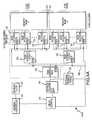
- FIGS. 1 and 1AA simplified view of a typical, conventional DRAM memory array is depicted in FIGS. 1 and 1A. Both show part of a 256 Mb array 110 which stores data in two conventional DRAM memory banks 112 and 114 .
- Each memory bank 112 and 114for example, has 8,192 rows of memory cells, for a total of 16,384 rows.
- the figuresare simplified most notably in the sense that they omit components such as column address multiplexers, column address latches, and column decoders.
- reading from or writing to a memory bankrequires both a row and a column address to identify the specific memory location where the data is or will be stored. Both row and column addressing circuits are needed to read from and write data to the memory banks.
- refreshing a memory bankis typically performed by reading and thereby refreshing an entire row at a time across each memory bank, and column addresses are irrelevant.
- the invention described in this applicationis directed to a system and method for refreshing a memory array, thus column addressing is not germane. Further discussion of column addressing means has been omitted for the sake of simplicity.
- a memory arraycan be refreshed in either a burst refresh mode or a distributed refresh mode.
- a burst refresh modeevery row of a memory array is sequentially refreshed in rapid succession. Then, after every passage of a predetermined interval, every row of the memory array again is refreshed in rapid succession.
- the maximum duration of the predetermined intervalis the span of time after which the data stored in the DRAM array begins to degrade less the time required to sequentially refresh every row in the array. This standard interval is necessarily brief considering the rapid refreshing needs of a conventional DRAM device.
- FIG. 1depicts a system memory which employs burst refresh.
- a refresh controller 120generates a refresh signal after the passage of the predetermined interval. Incremented by each pulse of a refresh clock 122 , a refresh counter 124 sequences through a series of 14-bit binary numbers. The 14-bit binary number equates to one of 2 14 or 16,384 numbers, one of which uniquely corresponds to the address of each row of one of the two memory banks 112 and 114 .
- Each row in the memory banks 112 and 114is accessed through a network of addressing circuitry 160 which includes a row address multiplexer 130 , row address latch A 150 , row address latch B 152 , and row decoders 132 - 142 .
- the row addressis directed by the row multiplexer 130 to row address latch A 150 or row address latch B 152 , respectively. From the appropriate row address latch 150 or 152 , five bits of the 14-bit address uniquely identify one of the 2 5 or sixteen row decoders 132 - 142 associated with each memory bank.
- the remaining nine bits of the addressuniquely correspond to one of the 2 9 or 512 rows addressed by each row decoder 132 - 142 . Only a few of the sixteen row decoders needed for each memory bank 112 and 114 are shown in the figures for the sake of visual clarity.
- a distributed refresh modeuses a distributed refresh mode to refresh one row of the memory array, then, after passage of a predetermined interval, the next row of the array is refreshed. This process is repeated until every row in the memory array is refreshed.
- the predetermined interval between the refreshing of each rowis far shorter than the predetermined interval between refresh cycles in a burst refresh context.
- the maximum duration of the predetermined interval between row refreshesis the span of time after which the data stored in the DRAM array begins to degrade, less the time required to sequentially refresh every row in the array, divided by the number of rows in the array. In other words, all other variables being equal, the predetermined interval in the distributed refresh mode would be equal to the predetermined interval in the burst refresh mode divided by the number of rows in the memory array.
- the predetermined interval between row refreshes in a distributed refreshwould be 1/8,192 as long as the predetermined interval between array refreshes in a burst refresh.
- FIG. 1Adepicts a system memory which employs distributed refresh.
- the refresh cycle in a distributed refresh modeis largely similar to the refresh cycle in a burst refresh mode, as reflected by how similar FIG. 1A is to FIG. 1 .
- the essential difference in a memory system employing distributed refreshis that there is not a single signal from the refresh controller 120 which initiates a refresh of the entire memory array. Instead, after each passage of the much shortened predetermined interval, the refresh controller 120 generates a refresh signal that causes one row of either memory bank A 112 or memory bank B 114 to be refreshed.
- the refresh controller 120instead of enabling a rapid count of the refresh counter 124 through its entire sequence, pulses the refresh counter 124 causing its count to be incremented by one.
- This row addressis passed to the addressing circuitry 160 which reads and thereby refreshes one row of the array in an identical manner as to how each row of the memory array is refreshed in a burst refresh. Then, after the passage of another much shortened predetermined interval, the refresh controller 120 emits another refresh signal which increments the refresh counter 124 , which, in turn, causes the next row in the memory array to be read and refreshed. This process repeats continually.
- PCDRAMprogrammable conductor dynamic random access memory
- FIG. 2AOne known form of PCDRAM memory cell 200 , as depicted in FIG. 2A, uses a conducting layer 202 , which may be comprised of silver, applied to an insulating layer 204 , which may be comprised of glass. The conducting layer 202 and insulating layer 204 are perpendicularly disposed in a frame of insulating material 206 .
- Conducting plates 208 and 210are disposed on outermost surfaces of the conducting layer 202 and insulating layer 204 , respectively. Tautologically, the conducting layer 202 conducts, whereas the insulating layer 204 does not conduct. When a low voltage is applied across the conducting plates 208 and 210 , the voltage will not be conducted because it will be blocked by the insulating layer 204 . Therefore, the memory cell is 200 not conductive in its initial state.
- FIG. 2Bdepicts the same memory cell 200 after a relatively high voltage has been applied.
- the relatively high positive voltageforces dendrils 212 of the material from the conducting layer 202 through the insulating layer 204 toward the conducting plate 210 disposed on the insulating layer 204 .
- Formation of the dendrils 212 of material from the conducting layer 202 through the insulating layer 204is caused by the charged metal particles being attracted and repelled by fields of differing or similar charge, respectively. This phenomenon is known, and will not be described further here in the interest of brevity.
- the cell 200becomes conductive.
- the cell 200will now conduct when even low voltages are applied, thus, this cell effectively now stores a logical one which later can be read by the system associated with the memory cell 200 .
- the memory cell 200can also be reprogrammed to store a logical zero. As shown in FIG. 2C, after application of a relatively high voltage of reverse polarity, i.e., with the positive voltage applied to the conducting plate 210 , reverses the migration of the dendrils 212 of material from the conducting layer. The dendrils 212 of material from the conducting layer 202 passing through the insulating layer 204 are forced back toward the conducting layer 202 and out of the insulating layer 204 by the same natural attraction and repulsion of charges which originally caused the cell to be programmed. This relatively high voltage of reverse polarity causes the memory cell 200 to become nonconductive once more. When a lesser voltage is applied, the memory cell 200 will no longer conduct. Thus, and the cell now effectively stores a logical zero. In sum, higher voltages of opposite sense can be used to program and reprogram these cells to conduct or not conduct, storing logical ones or zeroes, respectively.
- a relatively high voltage of reverse polarityi.e., with the positive
- the PCDRAM memory cell 200 describedis far less volatile than a conventional DRAM memory cell. Without being refreshed, a conventional DRAM cell only can maintain its logical bit for microseconds, while the PCDRAM memory cell 200 potentially can maintain its logical bit for days. Eventually, natural diffusion of the material from the conducting layer 202 into and out of the insulating layer 204 resulting from ordinary atomic motion will corrupt the data stored. Nonetheless, PCDRAM devices need only be refreshed after an extended interval, thus, less power is needed to refresh these devices than is needed for the frequent refreshing required by conventional DRAM devices.
- refresh signal delay meansan array comprised of less volatile DRAM devices, which only need to be refreshed after an extended interval, can be refreshed less frequently, consuming less power, while still using conventional DRAM refreshing control circuitry.
- the delay meansdelays externally generated refresh signals supplied to accommodate the refresh rate required by conventional DRAM memory devices but, in response, generates far less frequent delayed refresh signals. This reduces the frequency with which the less volatile DRAM devices will be refreshed, and powers off supporting addressing circuitry when it is not needed. Therefore, the delay means allows computing systems designed to use conventional DRAM devices to work with DRAM devices which only need to be refreshed after an extended interval and reduces the amount power wasted through unnecessarily frequent refresh cycles.
- FIG. 1is a simplified block diagram of a section of a conventional DRAM memory array that may be adapted to use the invention in a burst refresh mode.
- FIG. 1Ais a simplified block diagram of a section of a conventional DRAM memory array that may be adapted to use the invention in a distributed refresh mode.
- FIG. 2Ais a cross-sectional view of a known programmable conductor DRAM (PCDRAM) memory cell in its initial state before the application of a voltage that can be used to write to the cell that may be used with the invention.
- PCDRAMprogrammable conductor DRAM
- FIG. 2Bis a cross-sectional view of the PCDRAM cell depicted in FIG. 2A after a high voltage has been applied to the cell to write a logical one to the cell.
- FIG. 2Cis a cross-sectional view of the PCDRAM cell depicted in FIG. 2B after a high voltage of polarity opposite to that applied to cause the state depicted in FIG. 2B has been applied to the cell to write a logical zero to the cell.
- FIG. 3is a symbolic block diagram generally representing the functioning of embodiments of the present invention.
- FIG. 4is a block diagram of the same section of a DRAM memory array depicted in FIG. 1 replacing the conventional DRAM devices with DRAM devices which only need to be refreshed after an extended interval and adapted with a first embodiment of the invention to reduce the power needed to refresh the memory array using a burst refresh mode.
- FIG. 4Ais a block diagram of the same section of a DRAM memory array depicted in FIG. 1 replacing the conventional DRAM devices with DRAM devices which only need to be refreshed after an extended interval and adapted with a first embodiment of the invention to reduce the power needed to refresh the memory array using a distributed refresh mode.
- FIG. 5is a timing diagram of the first embodiment of the invention to reflect the reduction in state changes made possible by the first embodiment of the invention.
- FIG. 6is a block diagram of the same section of a DRAM memory array depicted in FIG. 4 further adapted with a second embodiment of the invention to save additional power in refreshing the memory array using a burst refresh mode.
- FIG. 6Ais a block diagram of the same section of a DRAM memory array depicted in FIG. 4 further adapted with a second embodiment of the invention to save additional power in refreshing the memory array using a distributed refresh mode.
- FIG. 7is a timing diagram of the second embodiment of the invention to reflect the reduction in state changes made possible by the second embodiment of the invention.
- FIG. 8is a block diagram of a computer system using a memory array employing DRAM devices which only need to be refreshed after an extended interval and a power saving memory device of an embodiment of the invention.
- FIG. 3represents the basic operation of embodiments of the present invention.
- External control devices designed to work with conventional DRAM deviceswill generate frequent conventional refresh signals. These conventional refresh signals 310 will be generated at a frequency f which corresponds to the rapidity with which conventional DRAM devices must be refreshed.
- Control systems designed to work with DRAM devices that only need to be refreshed after an extended intervalgenerate delayed refresh signals 320 far less often at a frequency f.
- conventional DRAM devicesmight need to be refreshed thousands of times per second, whereas DRAM devices such as PCDRAM cells may only need to be refreshed once per day. In this example, therefore, frequency f could be many orders of magnitude smaller than frequency f.
- the present inventionuses delay means 330 operable to receive the conventional refresh signals 310 and, at appropriately delayed intervals, generate the less frequent delayed refresh signals 320 .
- external devices designed to work with conventional DRAM devicesmay be used with DRAM devices which only need to be refreshed after an extended interval, without wasting power on unnecessarily frequent refresh cycles.
- FIG. 4depicts a memory array 410 very similar to the memory array 110 described in FIG. 1 .
- Identical components shown in FIG. 4have been provided with the same reference numeral, and explanation of their function and operation will not be repeated in the interest of brevity.
- the differences between the memory array 110 shown in FIG. 1 and the memory array 410 shown in FIG. 4are twofold.
- the memory array 410 depicted in FIG. 4has been adapted to use DRAM memory banks which only need to be refreshed after an extended interval 412 and 414 .
- a delay counter 420has been added to the memory array 410 .
- the memory array 410 shown in FIG. 4employs burst refresh, as does memory array 110 in FIG. 1 .
- the delay counter 420 shown in FIG. 4is a bit up counter which extends the interval between refresh cycles being conducted in the memory banks 412 and 414 , and powers off supporting circuitry when it is not needed.
- the delay counter 420extends the interval between refresh cycles by intercepting and counting the refresh signals being generated by the refresh controller 120 , the refresh controller 120 being responsive to externally applied refresh signals.
- the delay counter 420generates a delayed refresh signal to initiate a refresh cycle only after having counted a large, predetermined number of refresh signals from the refresh controller 120 . In effect, the overflow signal of the delay counter 420 becomes the actual refresh signal for the memory array 410 .
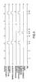
- FIG. 5shows how the delay counter 420 receives refresh signals from the refresh controller 120 and periodically generates a delayed refresh signal to trigger a refresh cycle.
- the refresh controller 120generates a refresh signal as often as is needed to refresh conventional DRAM memory banks 112 and 114 with which the conventional external circuitry (not shown) was designed to operate. In a conventional DRAM array, each pulse of the refresh controller 120 would trigger a refresh cycle for the entire memory array 410 .
- the refresh controller 120issues a refresh signal at intervals t 1 through t 10 , the refresh counter 124 and the addressing circuitry 160 , including the row multiplexer 130 , row address latches 150 and 152 , and row decoders 132 - 142 , remain powered off and no refresh cycle is conducted until t 3 . Instead, for each refresh signal generated by the refresh controller 120 , the delay counter 420 is incremented. The delayed refresh signal will be generated only when a desired number of refresh signals generated by the refresh controller 120 have been counted and skipped.
- the delay counter 420reaches its overflow count and the delay counter 420 overflow signal goes high.
- the overflow signal from the delay counter 420turns on the refresh counter 124 and the rest of the addressing circuitry 160 , including the row multiplexer 130 , row address latches 150 and 152 , and row decoders 132 - 142 .
- the refresh counter 124cycles through all 2 14 or 16,384 row addresses in the memory array 410 . Each address is passed to the row address multiplexer 130 which, in turn, directs the generated address to one of two row address latches 150 and 152 .
- the row address latches 150 and 152supply the row address to one of sixteen row address decoders 132 - 142 associated with each memory bank 410 and 412 .
- the overflow bit of the refresh counter 124goes high as depicted at t 4 of FIG. 5 .
- This overflow bitis fed back to the delay counter 420 and resets it.
- the delay counter 420once again begins counting the refresh signals generated by the refresh controller 120 , initiating a refresh cycle only after the delay counter 420 again reaches its overflow count.
- a suitably large delay counter 420could be used so that the delay counter 420 would only overflow as often as needed to refresh the memory banks 412 and 414 only after an extended interval.
- the addressing circuitry 160including the row multiplexer 130 , the row address latches 150 and 152 , and the row decoders 132 - 142 , all can be left powered off except as needed. Unneeded refresh signals generated by the refresh controller 120 , as shown at t 1 , t 2 , t 5 , and t 8 in FIG. 5, can be ignored, and the addressing circuitry left powered off. Power need not be supplied to the addressing circuitry 160 until the delay counter 420 reaches overflow and indicates the addressing circuitry 160 needs to be powered on, as shown at t 3 and again at t 9 . The addressing circuitry 160 can be powered off at the conclusion of each of the refresh cycles, as shown at t 4 and t 10 in FIG. 5 .
- the addressing circuitry 160still will be needed to perform memory read or write operations, as signaled by the external address signal 126 as shown at t 6 . However, because the refresh counter 124 is not needed for a memory read or write operation, the refresh counter 124 can still be left powered off at these times.
- the addressing circuitry 160will be powered on by the delay counter 420 or the external address signal 126 . If the power sourced by the overflow signal of the delay counter 420 or external address signal 126 is not sufficient to power the addressing circuitry 160 , the overflow signal of the delay counter 420 or the external address signal 126 can be used to enable a transistor having sufficient power-handling capability to power these circuits. Use of a transistor or other device which can supply more power, switched by the output of another circuit, is well known in the art and will not be described here further for the sake of brevity.
- FIG. 4Adepicts a similar memory array 410 A adapted to use the first embodiment of the invention in a distributed refresh mode.
- the refresh counter 124is pulsed by the delay counter 420 instead of the refresh clock 122 .
- each refresh signal issued by the refresh controller 120causes one single row of the memory banks 412 and 414 to be refreshed at a time instead of all the rows being refreshed in a single sequence.
- the delay counter 420will count a large, predetermined number of these signals before initiating the refresh sequence for the next row in the memory array.
- the interval between refresh sequences initiated by the delay counter 420will be 1/8,192 as long as the interval between refresh sequences initiated by the delay counter 420 for the memory array 410 .
- the refresh counter 124is not powered on and off by the delay counter 420 . Using distributed refresh, the refresh counter 124 must constantly maintains its row count. Third, in the memory array 410 A, an overflow output of the refresh counter 124 is not needed.
- the first embodiment of the inventionprovides three significant advantages.
- the embodiment of FIG. 4allows the use of conventional refreshing circuitry only by adding the delay counter 420 to control the enabling of the addressing circuitry 160 .
- Third, power consumed by the addressing circuitry 160is reduced because these devices would be powered off when not in use.
- a second embodiment of the invention shown in FIG. 6shows how additional power can be saved by selectively powering on only parts of the addressing circuitry 660 during a refresh cycle.
- the first embodiment of the inventionwhen either the delay counter 420 reaches overflow, all of the addressing circuitry 160 is powered on, regardless of which row of which memory bank 412 or 414 is to be accessed. In other words, whenever the memory banks 412 or 414 are accessed, thirty-five different devices are powered on, including the row address multiplexer 130 , two row address latches 150 and 152 , and thirty-two row decoders 132 - 142 .
- the memory array 410stores just one bit of what presumably is at least an eight-bit word, then at least eight times as many devices would be powered on each time the memory is accessed for a read, write, or refresh operation, even though only one row can be read from, written to, or refreshed at one time.
- This second embodimentuses five additional control devices to control addressing of the memory array during refresh cycles, only three of which are powered on at one time when using a burst refresh mode. These additional devices allow for only six supporting devices to be activated at a time during a refresh cycle instead of thirty-five. This saves the wasteful powering and heat generation of twenty-nine superfluous devices. For a memory array eight bits in width, forty-eight devices would only need to be powered on at one time instead of two-hundred and eighty.
- FIG. 6depicts a memory array 610 very similar to the memory array 410 described in FIG. 4 .
- PCDRAM memory bankswhich only need to be refreshed after an extended interval 412 and 414 still are being used, and to take advantage of their lower volatility, a delay counter 420 again is employed to extend the interval between refresh cycles.
- Five devicesare added to the memory array 610 shown in FIG. 6 : a bank segment bit up counter 670 , two row bit up counters 680 and 682 , and two row decoder selectors 690 and 692 . The purpose of these devices is to selectively power on only the row decoder 132 - 142 that is needed at any one point of a refresh cycle.
- These row decoders 132 - 142constitute thirty-two of the thirty-five devices or 90% of the addressing circuitry 160 (FIGS. 1 and 4) conventionally used to sequentially address a memory array during a refresh cycle.
- the sample memory array 610again includes two memory banks 412 and 414 , each of which comprises, for example, 8,196 rows of memory cells. Associated with each of the memory banks 412 and 414 are sixteen row decoders 132 - 142 . Each row decoder addresses 512 rows of a memory bank. To sequentially access each of the row decoders 132 - 142 , a four-bit counter is needed to sequentially generate a code for each of the 2 4 or sixteen counters. This embodiment of the invention includes two four-bit row bit up counters 680 and 682 , one to generate the address of each of the sixteen row decoders 132 - 142 for each memory bank 412 and 414 .
- each of the two counters 680 and 682is a four-bit demultiplexer which serves as a row decoder selector 690 and 692 .
- these row decoder selectorswill activate one bit of a sixteen-bit wide output as is well known in the art.
- row bit up counter A 680 and row decoder selector A 690 , and row bit up counter B 682 and row bit up decoder B 692can selectively and sequentially power on each of the sixteen bit row decoders 132 - 142 for each of their respective memory banks 412 and 414 , one row at a time.
- FIG. 7shows how the delay counter 420 receives refresh signals from the refresh controller 120 , periodically triggers a refresh cycle, and governs the selective powering on of the addressing circuitry 660 .
- FIG. 7details a shorter interval of time to highlight the sequential powering on of the individual row decoders 132 - 142 during a refresh cycle.
- the refresh signals generated by the refresh controller 120are not shown; it will be appreciated that the refresh controller 120 necessarily continues to generate refresh signals, but depiction of its signal has been eliminated from this figure for the sake of simplicity.
- the delay counter 420has counted the large, predetermined number of refresh signals generated by the refresh controller 120 to warrant initiating a refresh sequence for the DRAM memory banks which only need to be refreshed after an extended interval 412 and 414 .
- the overflow signal of the delay counter 420goes high and powers on the refresh counter 124 , the row address multiplexer 130 , and the row address latches 150 and 152 .
- the overflow signal generated by the delay counter 420does not power on each of the row decoders 132 - 142 . Instead, this overflow signal powers on row bit up counter A 680 , row decoder selector A 690 , and the bank segment bit up counter 670 .
- row decoder selector AWith row bit up counter A 680 powered on in its initial state, it supplies a count of four zeroes to row decoder selector A 690 . Row decoder selector A therefore activates row decoder A 0 132 . Because it is active, row decoder A 0 132 is able to sequentially address each of the 2 9 or 512 rows that it addresses in memory bank A 412 . These row addresses are supplied to row decoder A 0 132 by row address latch A 150 , which has received that address from the row address multiplexer 130 . The row address multiplexer 130 has generated this address by decoding the count provided to it by the refresh counter 124 .
- the bank segment bit up counter 670is a nine-bit counter that will reach overflow after counting 2 9 or 512 pulses of the refresh clock 122 .
- the overflow of the bank segment bit up counter 670is connected to both the row bit up counters 680 and 682 .
- the overflow signal from the bank segment bit up counter 670can increment row bit up counters 680 and 682 after every 512 pulses of the refresh clock 122 have enabled the refreshing of each of the 512 rows in the memory bank segment addressed by each of the row decoders 132 - 142 .
- the same refresh clock 122pulses the bank segment bit up counter 670 and the refresh counter 124 .
- the nine-bit count maintained by the bank segment bit up counter 670 and the nine least significant bits of the count maintained by the refresh counter 124will be synchronized. Because they are synchronized, with the completion of each nine-bit count, the bank segment bit up counter 670 will overflow to increment the appropriate row bit up counter 680 and 682 , in turn enabling the appropriate row decoder selector 690 and 692 to activate the appropriate row decoder 132 - 142 , while the refresh counter 124 continues to count the rows it refreshes throughout the memory array 610 .
- the bank segment bit up counter 670has sequenced through its entire nine-bit sequence and generates an overflow signal.
- This overflow signalincrements row bit up counter A 680 .
- row decoder selector A 690generates a different sixteen-bit code which powers off row decoder A 0 132 and powers on row decoder A 1 134 .
- the refresh counter 124sequences through the nine least significant bits of its count for the second time. This time, however, the nine least significant bits of the count generated by refresh counter 124 are applied through row decoder A 1 134 and serve to address and refresh the next 512 rows of memory bank A 412 .
- row decoder A 1 134is then powered off while the next row decoder A 2 (not shown in FIG. 6) is powered on, while all the other row decoders 132 - 142 remain powered off.
- row bit up counter A 680reaches overflow. As shown in FIG. 7, this overflow signal powers on row decoder selector B 682 and its associated row decoder selector 692 .
- a simple latchcould be used to preserve the high overflow signal generated by row bit up counter A 680 to maintain power to row bit up counter B 682 and its associated row decoder selector B 692 while powering off row bit up counter A 680 and row decoder selector A 690 .
- row bit up counter B 682when it is powered on at t 4 , row bit up counter B 682 supplies a count of four zeroes to row decoder selector B 692 .
- Row decoder selector B 692activates row decoder B 0 138 .
- Row decoder B 0 138then sequentially addresses each of the 512 rows of memory bank A 412 that it serves. These row addresses are supplied to row decoder B 0 138 by row address latch B 152 , which has received that address from the row address multiplexer 130 .
- the row address multiplexer 130has generated this address by decoding the count provided to it by the refresh counter 124 .
- the bank segment bit up counter 670has sequenced through its nine-bit count and reached overflow.
- This overflow signalcauses row bit up counter B 682 to increment, in turn causing row decoder selector B 692 to power off row decoder B 0 138 and activate row decoder B 1 140 .
- the repeated overflow of the bank segment bit up counter 670activates one at a time the sixteen address decoders 138 - 142 associated with memory bank B 414 , while each addresses the 512 rows it serves in associated memory bank B 414 .
- each row decoder 132 - 142has addressed and refreshed all 512 rows it serves, the refresh counter 124 reaches overflow, and the refresh cycle is complete.
- Overflow of the refresh counter 124powers off the addressing circuitry 660 and the refresh counter 124 .
- One difference in the second embodimentis that fewer devices in the addressing circuitry 660 will be turned off upon overflow of the refresh counter 124 .
- all the addressing circuitry 660is powered up. In this embodiment, all of the circuitry is powered up so that each of the memory banks 412 and 414 can be accessed quickly, without the processor or controller generating the external address signal 126 having to wait for the sequential activation of row decoders 132 - 142 which would slow system processing throughput.
- the memory access initiated by receipt of the external address signal 126is completed at t 8 , and all of the addressing circuitry 660 is powered off.
- FIG. 6Adepicts a similar memory array 610 A adapted to use the first embodiment of the invention in a distributed refresh mode.
- the refresh counter 124is pulsed by the delay counter 420 instead of the refresh clock 122 .
- the refresh counter 124 , the row segment bit up counter 670 , and row bit up counter A 680 and row bit up counter B 682are not powered on and off by the delay counter 420 .
- the refresh counter 124 and the bank segment bit up counter 670must constantly maintain their row counts.
- row bit up counter A 680 or row bit up counter B 682whichever is currently active, must remain powered on to maintain its count of which of the row decoders 132 - 142 should be activated when the next row is refreshed.
- the overflow output of row bit up counter A 680can be used to power on row bit up counter B 682
- the overflow output of row bit up counter B 682can be used to power on row bit up counter A 680 so that the one not being used does not need to be powered on at all times.
- both row bit up counters 680 and 682could be left powered on at all times. Accordingly, using distributed refresh mode, three or four additional devices will need to be powered on at all times.
- an overflow output of the refresh counter 124is not needed.
- the inventionalso could be embodied in other forms.
- One example not shown in the figurescould be a hybrid form using a series of distributed refresh signals generated by the refresh controller to perform, in essence, a slow burst refresh of the array after the passage of an extended interval.
- the refresh controllerwould be programmed to generate row refresh signals after the passage of a suitable interval for a conventional DRAM array.
- the delay counterwould intercept, count, and ignore a number of these distributed refresh signals until the passage of an extended interval by when the less volatile memory devices would have to be refreshed.
- the number of refresh signals from the refresh controller to be ignoredwould be determined by the duration of the extended interval divided by the duration between refresh signals generated by the refresh controller for a conventional DRAM memory array.
- the delay counterAfter the extended interval had passed, the delay counter would pass the refresh signals from the refresh controller through to the refresh counter. This could be handled by connecting the overflow signal from the delay counter and the refresh signal from the refresh controller to an AND gate, the output of which would become the input pulse to the refresh controller. After counting a number of refresh signals corresponding to the extended interval causing the delay counter's overflow signal to go high, the refresh signals would cause a high output from the AND gate which, in turn, would pulse the refresh counter. The rows of the less volatile memory array would then be refreshed sequentially as pulsed by the row refresh signals from the refresh controller. In other words, the memory array would be refreshed in one slow, sequential burst in rhythm to the row refresh signals from the refresh controller after the passage of an extended interval. Once all the rows were refreshed, the delay counter would reset, and proceed to ignore another long sequence of row refresh commands from the refresh controller until the less volatile memory array once again needed to be refreshed.
- FIG. 8is a block diagram of a computer system 810 that includes a processor 812 for performing various computing functions by executing software to perform specific calculations or tasks.
- the processor 812is coupled to a processor bus 814 that normally includes an address bus, a control bus, and a data bus (not separately shown).
- the computer system 810includes a system memory 816 , which could be the memory array 410 of FIG. 4 or the memory array 610 of FIG. 6, both of which use DRAM devices which only need to be refreshed after an extended interval, such as PCDRAM devices, and supporting circuitry which enables the power savings previously described.
- the system memory 816is coupled to the processor bus 814 by a system controller 820 or similar device, which is also coupled to an expansion bus 822 , such as a Peripheral Component Interface (“PCI”) bus.
- a bus 726 coupling the system controller 820 to the system memory 816also normally includes an address bus, a control bus, and a data bus (not separately shown), although other architectures can be used.
- the data bus of the system memory 816may be coupled to the data bus of the processor bus 814 , or the system memory 816 may be implemented by a packetized memory (not shown), which normally does not include a separate address bus and control bus.
- the computer system 810also includes one or more input devices 834 , such as a keyboard or a mouse, coupled to the processor 812 through the expansion bus 822 , the system controller 820 , and the processor bus 814 . Also typically coupled to the expansion bus 822 are one or more output devices 836 , such as a printer or a video terminal.
- One or more data storage devices 838are also typically coupled to the expansion bus 822 to allow the processor 812 to store data or retrieve data from internal or external storage media (not shown). Examples of typical storage devices 838 include hard and floppy disks, tape cassettes, and compact disk read-only memories (CD-ROMs).
- the processor 812is also typically coupled to cache memory 840 through the processor bus 814 .
- PCDRAM devicesunlike conventional DRAM devices 112 and 114 , PCDRAM devices also must be signaled as to when they are being refreshed as opposed to merely being read. The reason for this, as was previously described, is one of the inherent differences between conventional DRAM devices and PCDRAM devices.
- a conventional DRAM memory cellreading a memory cell through an associated sense amplifier simultaneously and automatically refreshes that cell. Accordingly, presented with a row address, a conventional DRAM device will read the cells in that row, and, coincidentally, refresh the cells in that row.
- a PCDRAM devicecannot be refreshed simply by reading it.
- a higher voltage than carried by read signals in the devicemust be applied to cause the formation or reformation of dendrils 212 (FIG. 2 B).
- the memory banks 412 and 414must be signaled that this is not an ordinary read signal, but that the addresses in that row must be read and refreshed with the application of a higher voltage, as previously described.
- PCDRAM devicesthemselves can be powered off when not being accessed. PCDRAM devices store their data bits by undergoing a physical transformation as previously described. Thus, they can be turned off when not in use.
- memory bank A 412 and memory bank B 414could be powered on and off by the same delay counter 420 overflow signal that powered on the addressing circuitry 160 .
- memory bank A 412could be powered on by the same delay counter 420 overflow signal that powers on row bit up decoder A 680 and row decoder selector A 690 , and powered off by the same row bit up counter A 680 overflow signal that powers off row bit up decoder A 680 and row decoder selector A 690 .
- memory bank B 414could be powered on by the same row bit up counter A 680 overflow signal that powers on row bit up decoder B 682 and row decoder selector B 692 , and powered off by the same refresh counter 124 overflow signal that powers off row bit up decoder B 682 and row decoder selector B 692 .
- the first embodiment of the inventionsaves power by extending the time between refresh cycles to exploit less volatile DRAM devices which need to be refreshed only after an extended interval.
- the first embodimentaccomplishes this predominantly through the use of a delay counter which delays the refresh signals generated by a conventional refresh controller designed for conventional DRAM memory devices, and generates refresh signals much less frequently.
- the second embodiment of the inventionfurther saves power during each refresh cycle by sequentially activating only the row decoders needed to address the rows currently being refreshed rather than powering on all the row decoders at once.
Landscapes
- Engineering & Computer Science (AREA)
- Microelectronics & Electronic Packaging (AREA)
- Computer Hardware Design (AREA)
- Dram (AREA)
Abstract
Description
Claims (143)
Priority Applications (2)
| Application Number | Priority Date | Filing Date | Title |
|---|---|---|---|
| US10/002,707US6560155B1 (en) | 2001-10-24 | 2001-10-24 | System and method for power saving memory refresh for dynamic random access memory devices after an extended interval |
| US10/418,945US6930944B2 (en) | 2001-10-24 | 2003-04-18 | System and method for power saving memory refresh for dynamic random access memory devices after an extended interval |
Applications Claiming Priority (1)
| Application Number | Priority Date | Filing Date | Title |
|---|---|---|---|
| US10/002,707US6560155B1 (en) | 2001-10-24 | 2001-10-24 | System and method for power saving memory refresh for dynamic random access memory devices after an extended interval |
Related Child Applications (1)
| Application Number | Title | Priority Date | Filing Date |
|---|---|---|---|
| US10/418,945ContinuationUS6930944B2 (en) | 2001-10-24 | 2003-04-18 | System and method for power saving memory refresh for dynamic random access memory devices after an extended interval |
Publications (2)
| Publication Number | Publication Date |
|---|---|
| US20030076725A1 US20030076725A1 (en) | 2003-04-24 |
| US6560155B1true US6560155B1 (en) | 2003-05-06 |
Family
ID=21702081
Family Applications (2)
| Application Number | Title | Priority Date | Filing Date |
|---|---|---|---|
| US10/002,707Expired - LifetimeUS6560155B1 (en) | 2001-10-24 | 2001-10-24 | System and method for power saving memory refresh for dynamic random access memory devices after an extended interval |
| US10/418,945Expired - LifetimeUS6930944B2 (en) | 2001-10-24 | 2003-04-18 | System and method for power saving memory refresh for dynamic random access memory devices after an extended interval |
Family Applications After (1)
| Application Number | Title | Priority Date | Filing Date |
|---|---|---|---|
| US10/418,945Expired - LifetimeUS6930944B2 (en) | 2001-10-24 | 2003-04-18 | System and method for power saving memory refresh for dynamic random access memory devices after an extended interval |
Country Status (1)
| Country | Link |
|---|---|
| US (2) | US6560155B1 (en) |
Cited By (24)
| Publication number | Priority date | Publication date | Assignee | Title |
|---|---|---|---|---|
| US20030217246A1 (en)* | 2002-05-17 | 2003-11-20 | Kenichi Kubota | Memory control apparatus, method and program |
| US20040032782A1 (en)* | 2001-10-24 | 2004-02-19 | Glen Hush | System and method for power saving memory refresh for dynamic random access memory devices after an extended interval |
| US20040071012A1 (en)* | 2001-08-30 | 2004-04-15 | Gilton Terry L. | Method of retaining memory state in a programmable conductor RAM |
| US20050201146A1 (en)* | 2003-07-08 | 2005-09-15 | Moore John T. | Method of refreshing a PCRAM memory device |
| US20050237838A1 (en)* | 2004-04-27 | 2005-10-27 | Jong-Tae Kwak | Refresh control circuit and method for multi-bank structure DRAM |
| US20050249010A1 (en)* | 2004-05-06 | 2005-11-10 | Klein Dean A | Memory controller method and system compensating for memory cell data losses |
| US6965537B1 (en) | 2004-08-31 | 2005-11-15 | Micron Technology, Inc. | Memory system and method using ECC to achieve low power refresh |
| US20050289444A1 (en)* | 2004-06-25 | 2005-12-29 | Klein Dean A | Low power cost-effective ECC memory system and method |
| US20060010339A1 (en)* | 2004-06-24 | 2006-01-12 | Klein Dean A | Memory system and method having selective ECC during low power refresh |
| US20060013052A1 (en)* | 2004-07-15 | 2006-01-19 | Klein Dean A | Method and system for controlling refresh to avoid memory cell data losses |
| US20060104137A1 (en)* | 2004-11-12 | 2006-05-18 | International Business Machines Corporation | Deferring refreshes during calibrations in XDRTM memory systems |
| US20060158948A1 (en)* | 2005-01-19 | 2006-07-20 | Elpida Memory, Inc | Memory device |
| US20060221759A1 (en)* | 2005-03-11 | 2006-10-05 | Micron Technology, Inc. | Circuit and method for operating a delay-lock loop in a power saving manner |
| US20060291297A1 (en)* | 2002-07-15 | 2006-12-28 | Fujitsu Limited | Semiconductor memory |
| US20070186030A1 (en)* | 2001-02-13 | 2007-08-09 | Stmicroelectronics S.A. | Fast random access DRAM management method |
| US20070279975A1 (en)* | 2006-06-06 | 2007-12-06 | Hudgens Stephen J | Refreshing a phase change memory |
| US20080092016A1 (en)* | 2006-10-11 | 2008-04-17 | Micron Technology, Inc. | Memory system and method using partial ECC to achieve low power refresh and fast access to data |
| US20080109705A1 (en)* | 2006-10-18 | 2008-05-08 | Pawlowski J Thomas | Memory system and method using ECC with flag bit to identify modified data |
| US20080222483A1 (en)* | 2007-03-08 | 2008-09-11 | Micron Technology, Inc. | Method, system, and apparatus for distributed decoding during prolonged refresh |
| CN103197753A (en)* | 2013-03-25 | 2013-07-10 | 西安华芯半导体有限公司 | Power saving method of DRAM (Dynamic Random Access Memory) |
| US20150009769A1 (en)* | 2013-07-05 | 2015-01-08 | Qualcomm Incorporated | Dram sub-array level refresh |
| US9541978B2 (en) | 2014-06-13 | 2017-01-10 | Seagate Technology Llc | Redundancies for reconstruction in mass data storage systems |
| US10467172B2 (en) | 2016-06-01 | 2019-11-05 | Seagate Technology Llc | Interconnect for shared control electronics |
| US12093546B2 (en) | 2021-03-02 | 2024-09-17 | Seagate Technology Llc | Operating multiple storage devices using NVM interface |
Families Citing this family (15)
| Publication number | Priority date | Publication date | Assignee | Title |
|---|---|---|---|---|
| KR100543914B1 (en)* | 2003-04-30 | 2006-01-23 | 주식회사 하이닉스반도체 | Semiconductor memory device that can reduce peak current during refresh operation |
| KR100564633B1 (en)* | 2004-09-25 | 2006-03-28 | 삼성전자주식회사 | Semiconductor memory device having improved operation performance and access control method thereof |
| US7158434B2 (en)* | 2005-04-29 | 2007-01-02 | Infineon Technologies, Ag | Self-refresh circuit with optimized power consumption |
| US7366047B2 (en)* | 2005-11-09 | 2008-04-29 | Infineon Technologies Ag | Method and apparatus for reducing standby current in a dynamic random access memory during self refresh |
| US7599208B2 (en)* | 2006-07-27 | 2009-10-06 | Hynix Semiconductor Inc. | Nonvolatile ferroelectric memory device and refresh method thereof |
| US7505349B2 (en)* | 2006-09-07 | 2009-03-17 | Honeywell International Inc. | Refresh sequence control for multiple memory elements |
| FR2932006B1 (en)* | 2008-06-03 | 2010-06-11 | E2V Semiconductors | MATRIX INTEGRATED CIRCUIT WITH MIXED DECODING |
| US9721640B2 (en) | 2015-12-09 | 2017-08-01 | Intel Corporation | Performance of additional refresh operations during self-refresh mode |
| US10297307B1 (en)* | 2017-12-29 | 2019-05-21 | Micron Technology, Inc. | Methods for independent memory bank maintenance and memory devices and systems employing the same |
| US11189662B2 (en) | 2018-08-13 | 2021-11-30 | Micron Technology | Memory cell stack and via formation for a memory device |
| US10991425B2 (en) | 2018-08-13 | 2021-04-27 | Micron Technology, Inc. | Access line grain modulation in a memory device |
| US11373695B2 (en) | 2019-12-18 | 2022-06-28 | Micron Technology, Inc. | Memory accessing with auto-precharge |
| US11568913B2 (en)* | 2020-02-05 | 2023-01-31 | Micron Technology, Inc. | Voltage adjustment based on pending refresh operations |
| US11430950B2 (en) | 2020-03-27 | 2022-08-30 | Micron Technology, Inc. | Low resistance via contacts in a memory device |
| US11798609B2 (en)* | 2021-08-06 | 2023-10-24 | Winbond Electronics Corp. | Semiconductor memory device including control unit controlling time interval of refresh operation on memory to shorten interval between memory refresh operations corresponding to read/write access requirement |
Citations (4)
| Publication number | Priority date | Publication date | Assignee | Title |
|---|---|---|---|---|
| US5031147A (en)* | 1988-07-26 | 1991-07-09 | Kabushiki Kaisha Toshiba | Semiconductor memory |
| US5991851A (en)* | 1997-05-02 | 1999-11-23 | Enhanced Memory Systems, Inc. | Enhanced signal processing random access memory device utilizing a DRAM memory array integrated with an associated SRAM cache and internal refresh control |
| US6310819B1 (en)* | 1997-08-22 | 2001-10-30 | Micron Technology, Inc. | Method and apparatus for controlling the operation of an integrated circuit responsive to out-of-synchronism control signals |
| US6392948B1 (en)* | 1996-08-29 | 2002-05-21 | Micron Technology, Inc. | Semiconductor device with self refresh test mode |
Family Cites Families (13)
| Publication number | Priority date | Publication date | Assignee | Title |
|---|---|---|---|---|
| US6724654B1 (en)* | 2000-08-14 | 2004-04-20 | Micron Technology, Inc. | Pulsed write techniques for magneto-resistive memories |
| US6646902B2 (en) | 2001-08-30 | 2003-11-11 | Micron Technology, Inc. | Method of retaining memory state in a programmable conductor RAM |
| US6560155B1 (en) | 2001-10-24 | 2003-05-06 | Micron Technology, Inc. | System and method for power saving memory refresh for dynamic random access memory devices after an extended interval |
| US6791859B2 (en) | 2001-11-20 | 2004-09-14 | Micron Technology, Inc. | Complementary bit PCRAM sense amplifier and method of operation |
| US6873538B2 (en) | 2001-12-20 | 2005-03-29 | Micron Technology, Inc. | Programmable conductor random access memory and a method for writing thereto |
| US6909656B2 (en) | 2002-01-04 | 2005-06-21 | Micron Technology, Inc. | PCRAM rewrite prevention |
| US6791885B2 (en) | 2002-02-19 | 2004-09-14 | Micron Technology, Inc. | Programmable conductor random access memory and method for sensing same |
| US6891749B2 (en) | 2002-02-20 | 2005-05-10 | Micron Technology, Inc. | Resistance variable ‘on ’ memory |
| US6849868B2 (en) | 2002-03-14 | 2005-02-01 | Micron Technology, Inc. | Methods and apparatus for resistance variable material cells |
| US6751114B2 (en) | 2002-03-28 | 2004-06-15 | Micron Technology, Inc. | Method for programming a memory cell |
| US6864500B2 (en) | 2002-04-10 | 2005-03-08 | Micron Technology, Inc. | Programmable conductor memory cell structure |
| US6731528B2 (en) | 2002-05-03 | 2004-05-04 | Micron Technology, Inc. | Dual write cycle programmable conductor memory system and method of operation |
| US7010644B2 (en) | 2002-08-29 | 2006-03-07 | Micron Technology, Inc. | Software refreshed memory device and method |
- 2001
- 2001-10-24USUS10/002,707patent/US6560155B1/ennot_activeExpired - Lifetime
- 2003
- 2003-04-18USUS10/418,945patent/US6930944B2/ennot_activeExpired - Lifetime
Patent Citations (4)
| Publication number | Priority date | Publication date | Assignee | Title |
|---|---|---|---|---|
| US5031147A (en)* | 1988-07-26 | 1991-07-09 | Kabushiki Kaisha Toshiba | Semiconductor memory |
| US6392948B1 (en)* | 1996-08-29 | 2002-05-21 | Micron Technology, Inc. | Semiconductor device with self refresh test mode |
| US5991851A (en)* | 1997-05-02 | 1999-11-23 | Enhanced Memory Systems, Inc. | Enhanced signal processing random access memory device utilizing a DRAM memory array integrated with an associated SRAM cache and internal refresh control |
| US6310819B1 (en)* | 1997-08-22 | 2001-10-30 | Micron Technology, Inc. | Method and apparatus for controlling the operation of an integrated circuit responsive to out-of-synchronism control signals |
Cited By (83)
| Publication number | Priority date | Publication date | Assignee | Title |
|---|---|---|---|---|
| US20070186030A1 (en)* | 2001-02-13 | 2007-08-09 | Stmicroelectronics S.A. | Fast random access DRAM management method |
| US7436728B2 (en)* | 2001-02-13 | 2008-10-14 | Stmicroelectronics S.A. | Fast random access DRAM management method including a method of comparing the address and suspending and storing requests |
| US20040071012A1 (en)* | 2001-08-30 | 2004-04-15 | Gilton Terry L. | Method of retaining memory state in a programmable conductor RAM |
| US6813176B2 (en)* | 2001-08-30 | 2004-11-02 | Micron Technology, Inc. | Method of retaining memory state in a programmable conductor RAM |
| US20040032782A1 (en)* | 2001-10-24 | 2004-02-19 | Glen Hush | System and method for power saving memory refresh for dynamic random access memory devices after an extended interval |
| US6930944B2 (en) | 2001-10-24 | 2005-08-16 | Micron Technology, Inc. | System and method for power saving memory refresh for dynamic random access memory devices after an extended interval |
| US20030217246A1 (en)* | 2002-05-17 | 2003-11-20 | Kenichi Kubota | Memory control apparatus, method and program |
| US7295483B2 (en)* | 2002-07-15 | 2007-11-13 | Fujitsu Limted | Semiconductor memory |
| US20060291297A1 (en)* | 2002-07-15 | 2006-12-28 | Fujitsu Limited | Semiconductor memory |
| US20050201146A1 (en)* | 2003-07-08 | 2005-09-15 | Moore John T. | Method of refreshing a PCRAM memory device |
| US7385868B2 (en)* | 2003-07-08 | 2008-06-10 | Micron Technology, Inc. | Method of refreshing a PCRAM memory device |
| US7260010B2 (en)* | 2004-04-27 | 2007-08-21 | Hynix Semiconductor Inc. | Refresh control circuit and method for multi-bank structure DRAM |
| US20050237838A1 (en)* | 2004-04-27 | 2005-10-27 | Jong-Tae Kwak | Refresh control circuit and method for multi-bank structure DRAM |
| US7145827B2 (en)* | 2004-04-27 | 2006-12-05 | Hynix Semiconductor, Inc. | Refresh control circuit and method for multi-bank structure DRAM |
| US9064600B2 (en) | 2004-05-06 | 2015-06-23 | Micron Technology, Inc. | Memory controller method and system compensating for memory cell data losses |
| US20060056259A1 (en)* | 2004-05-06 | 2006-03-16 | Klein Dean A | Memory controller method and system compensating for memory cell data losses |
| US20060056260A1 (en)* | 2004-05-06 | 2006-03-16 | Klein Dean A | Memory controller method and system compensating for memory cell data losses |
| US20050249010A1 (en)* | 2004-05-06 | 2005-11-10 | Klein Dean A | Memory controller method and system compensating for memory cell data losses |
| US20090024884A1 (en)* | 2004-05-06 | 2009-01-22 | Micron Technology, Inc. | Memory controller method and system compensating for memory cell data losses |
| US8689077B2 (en) | 2004-05-06 | 2014-04-01 | Micron Technology, Inc. | Memory controller method and system compensating for memory cell data losses |
| US7099221B2 (en) | 2004-05-06 | 2006-08-29 | Micron Technology, Inc. | Memory controller method and system compensating for memory cell data losses |
| US7447974B2 (en) | 2004-05-06 | 2008-11-04 | Micron Technology, Inc. | Memory controller method and system compensating for memory cell data losses |
| US7836374B2 (en) | 2004-05-06 | 2010-11-16 | Micron Technology, Inc. | Memory controller method and system compensating for memory cell data losses |
| US20060069856A1 (en)* | 2004-05-06 | 2006-03-30 | Klein Dean A | Memory controller method and system compensating for memory cell data losses |
| US7447973B2 (en) | 2004-05-06 | 2008-11-04 | Micron Technology, Inc. | Memory controller method and system compensating for memory cell data losses |
| US7428687B2 (en) | 2004-05-06 | 2008-09-23 | Micron Technology, Inc. | Memory controller method and system compensating for memory cell data losses |
| US20060010339A1 (en)* | 2004-06-24 | 2006-01-12 | Klein Dean A | Memory system and method having selective ECC during low power refresh |
| US20060206769A1 (en)* | 2004-06-24 | 2006-09-14 | Klein Dean A | Memory system and method having selective ECC during low power refresh |
| US7461320B2 (en) | 2004-06-24 | 2008-12-02 | Micron Technology, Inc. | Memory system and method having selective ECC during low power refresh |
| US7526713B2 (en) | 2004-06-25 | 2009-04-28 | Micron Technology, Inc. | Low power cost-effective ECC memory system and method |
| US20050289444A1 (en)* | 2004-06-25 | 2005-12-29 | Klein Dean A | Low power cost-effective ECC memory system and method |
| US7340668B2 (en) | 2004-06-25 | 2008-03-04 | Micron Technology, Inc. | Low power cost-effective ECC memory system and method |
| US20060218469A1 (en)* | 2004-06-25 | 2006-09-28 | Klein Dean A | Low power cost-effective ECC memory system and method |
| US8446783B2 (en) | 2004-07-15 | 2013-05-21 | Micron Technology, Inc. | Digit line comparison circuits |
| US7898892B2 (en) | 2004-07-15 | 2011-03-01 | Micron Technology, Inc. | Method and system for controlling refresh to avoid memory cell data losses |
| US7280386B2 (en) | 2004-07-15 | 2007-10-09 | Micron Technology, Inc. | Method and system for controlling refresh to avoid memory cell data losses |
| US7272066B2 (en) | 2004-07-15 | 2007-09-18 | Micron Technology, Inc. | Method and system for controlling refresh to avoid memory cell data losses |
| US7623392B2 (en) | 2004-07-15 | 2009-11-24 | Micron Technology, Inc. | Method and system for controlling refresh to avoid memory cell data losses |
| US20080002503A1 (en)* | 2004-07-15 | 2008-01-03 | Klein Dean A | Method and system for controlling refresh to avoid memory cell data losses |
| US20060013052A1 (en)* | 2004-07-15 | 2006-01-19 | Klein Dean A | Method and system for controlling refresh to avoid memory cell data losses |
| US7277345B2 (en) | 2004-07-15 | 2007-10-02 | Micron Technology, Inc. | Method and system for controlling refresh to avoid memory cell data losses |
| US7558142B2 (en) | 2004-07-15 | 2009-07-07 | Micron Technology, Inc. | Method and system for controlling refresh to avoid memory cell data losses |
| US8279683B2 (en) | 2004-07-15 | 2012-10-02 | Micron Technology, Inc. | Digit line comparison circuits |
| US7116602B2 (en) | 2004-07-15 | 2006-10-03 | Micron Technology, Inc. | Method and system for controlling refresh to avoid memory cell data losses |
| US20060158950A1 (en)* | 2004-07-15 | 2006-07-20 | Klein Dean A | Method and system for controlling refresh to avoid memory cell data losses |
| US20060152989A1 (en)* | 2004-07-15 | 2006-07-13 | Klein Dean A | Method and system for controlling refresh to avoid memory cell data losses |
| US20060044913A1 (en)* | 2004-08-31 | 2006-03-02 | Klein Dean A | Memory system and method using ECC to achieve low power refresh |
| US7184352B2 (en) | 2004-08-31 | 2007-02-27 | Micron Technology, Inc. | Memory system and method using ECC to achieve low power refresh |
| US6965537B1 (en) | 2004-08-31 | 2005-11-15 | Micron Technology, Inc. | Memory system and method using ECC to achieve low power refresh |
| US7356642B2 (en)* | 2004-11-12 | 2008-04-08 | International Business Machines Corporation | Deferring refreshes during calibrations in memory systems |
| US20080140923A1 (en)* | 2004-11-12 | 2008-06-12 | Mark David Bellows | Deferring Refreshes During Calibrations in Memory Systems |
| US20060104137A1 (en)* | 2004-11-12 | 2006-05-18 | International Business Machines Corporation | Deferring refreshes during calibrations in XDRTM memory systems |
| US7613873B2 (en) | 2004-11-12 | 2009-11-03 | International Business Machines Corporation | Deferring refreshes during calibrations in memory systems |
| US20060158948A1 (en)* | 2005-01-19 | 2006-07-20 | Elpida Memory, Inc | Memory device |
| US20060250877A1 (en)* | 2005-03-11 | 2006-11-09 | Scott Smith | Circuit and method for operating a delay-lock loop in a power saving manner |
| US7218568B2 (en) | 2005-03-11 | 2007-05-15 | Micron Technology, Inc. | Circuit and method for operating a delay-lock loop in a power saving manner |
| US20060221759A1 (en)* | 2005-03-11 | 2006-10-05 | Micron Technology, Inc. | Circuit and method for operating a delay-lock loop in a power saving manner |
| US7177208B2 (en) | 2005-03-11 | 2007-02-13 | Micron Technology, Inc. | Circuit and method for operating a delay-lock loop in a power saving manner |
| US20070279975A1 (en)* | 2006-06-06 | 2007-12-06 | Hudgens Stephen J | Refreshing a phase change memory |
| US9286161B2 (en) | 2006-10-11 | 2016-03-15 | Micron Technology, Inc. | Memory system and method using partial ECC to achieve low power refresh and fast access to data |
| US7894289B2 (en) | 2006-10-11 | 2011-02-22 | Micron Technology, Inc. | Memory system and method using partial ECC to achieve low power refresh and fast access to data |
| US8832522B2 (en) | 2006-10-11 | 2014-09-09 | Micron Technology, Inc. | Memory system and method using partial ECC to achieve low power refresh and fast access to data |
| US8359517B2 (en) | 2006-10-11 | 2013-01-22 | Micron Technology, Inc. | Memory system and method using partial ECC to achieve low power refresh and fast access to data |
| US20080092016A1 (en)* | 2006-10-11 | 2008-04-17 | Micron Technology, Inc. | Memory system and method using partial ECC to achieve low power refresh and fast access to data |
| US8880974B2 (en) | 2006-10-18 | 2014-11-04 | Micron Technology, Inc. | Memory system and method using ECC with flag bit to identify modified data |
| US20080109705A1 (en)* | 2006-10-18 | 2008-05-08 | Pawlowski J Thomas | Memory system and method using ECC with flag bit to identify modified data |
| US8413007B2 (en) | 2006-10-18 | 2013-04-02 | Micron Technology, Inc. | Memory system and method using ECC with flag bit to identify modified data |
| US8601341B2 (en) | 2006-10-18 | 2013-12-03 | Micron Technologies, Inc. | Memory system and method using ECC with flag bit to identify modified data |
| US7900120B2 (en) | 2006-10-18 | 2011-03-01 | Micron Technology, Inc. | Memory system and method using ECC with flag bit to identify modified data |
| US8386886B2 (en) | 2007-03-08 | 2013-02-26 | Micron Technology, Inc. | Method, system, and apparatus for distributed decoding during prolonged refresh |
| US8042022B2 (en) | 2007-03-08 | 2011-10-18 | Micron Technology, Inc. | Method, system, and apparatus for distributed decoding during prolonged refresh |
| US20080222483A1 (en)* | 2007-03-08 | 2008-09-11 | Micron Technology, Inc. | Method, system, and apparatus for distributed decoding during prolonged refresh |
| CN103197753A (en)* | 2013-03-25 | 2013-07-10 | 西安华芯半导体有限公司 | Power saving method of DRAM (Dynamic Random Access Memory) |
| US20150009769A1 (en)* | 2013-07-05 | 2015-01-08 | Qualcomm Incorporated | Dram sub-array level refresh |
| US8982654B2 (en)* | 2013-07-05 | 2015-03-17 | Qualcomm Incorporated | DRAM sub-array level refresh |
| US9541978B2 (en) | 2014-06-13 | 2017-01-10 | Seagate Technology Llc | Redundancies for reconstruction in mass data storage systems |
| US9874915B2 (en) | 2014-06-13 | 2018-01-23 | Seagate Technology Llc | Extended file attributes for redundant data storage |
| US9880602B2 (en) | 2014-06-13 | 2018-01-30 | Seagate Technology Llc | Power characteristics in a system of disparate storage drives |
| US9939865B2 (en) | 2014-06-13 | 2018-04-10 | Seagate Technology Llc | Selective storage resource powering for data transfer management |
| US9965011B2 (en) | 2014-06-13 | 2018-05-08 | Seagate Technology Llc | Controller interface for operation of multiple storage drives |
| US10152105B2 (en) | 2014-06-13 | 2018-12-11 | Seagate Technology Llc | Common controller operating multiple storage drives |
| US10467172B2 (en) | 2016-06-01 | 2019-11-05 | Seagate Technology Llc | Interconnect for shared control electronics |
| US12093546B2 (en) | 2021-03-02 | 2024-09-17 | Seagate Technology Llc | Operating multiple storage devices using NVM interface |
Also Published As
| Publication number | Publication date |
|---|---|
| US20040032782A1 (en) | 2004-02-19 |
| US6930944B2 (en) | 2005-08-16 |
| US20030076725A1 (en) | 2003-04-24 |
Similar Documents
| Publication | Publication Date | Title |
|---|---|---|
| US6560155B1 (en) | System and method for power saving memory refresh for dynamic random access memory devices after an extended interval | |
| JP4979589B2 (en) | System and method for reducing power consumption during an extended refresh period of a dynamic random access memory device | |
| JP5767778B2 (en) | Memory with selective precharge | |
| US6711093B1 (en) | Reducing digit equilibrate current during self-refresh mode | |
| US11003361B2 (en) | Wear leveling | |
| US20200183791A1 (en) | Voltaile memory device and method for efficient bulk data movement, backup operation in the volatile memory device | |
| US20050105357A1 (en) | Method and circuit configuration for refreshing data in a semiconductor memory | |
| JP2013037760A (en) | Memory with front end precharge | |
| US7298661B2 (en) | Semiconductor memory device | |
| US6646941B1 (en) | Apparatus for operating an integrated circuit having a sleep mode | |
| EP1761932B1 (en) | Dram with half and full density operation | |
| KR102483906B1 (en) | Nas memory cell combined with nand flash memory and static random access memory and nas memory array using the same | |
| US20080080284A1 (en) | Method and apparatus for refreshing memory cells of a memory | |
| US8909849B2 (en) | Pipeline architecture for scalable performance on memory | |
| US7042786B2 (en) | Memory with adjustable access time | |
| US9361972B1 (en) | Charge level maintenance in a memory | |
| US20050035959A1 (en) | Method and apparatus for independentlyrefreshing memory capacitors | |
| US12423001B2 (en) | Memory device and operating method thereof | |
| US12362007B2 (en) | Memory controller support for mixed read | |
| US7561489B2 (en) | System and method of selective row energization based on write data | |
| US20250246214A1 (en) | Inrush current management in a memory array | |
| JPH09251783A (en) | Refresh control method, semiconductor memory device, and data processing device | |
| JPH09330595A (en) | Semiconductor storage device and data processing device |
Legal Events
| Date | Code | Title | Description |
|---|---|---|---|
| AS | Assignment | Owner name:MICRON TECHNOLOGY, INC., IDAHO Free format text:ASSIGNMENT OF ASSIGNORS INTEREST;ASSIGNOR:HUSH, GLEN;REEL/FRAME:012388/0846 Effective date:20011012 | |
| FEPP | Fee payment procedure | Free format text:PAYOR NUMBER ASSIGNED (ORIGINAL EVENT CODE: ASPN); ENTITY STATUS OF PATENT OWNER: LARGE ENTITY | |
| STCF | Information on status: patent grant | Free format text:PATENTED CASE | |
| CC | Certificate of correction | ||
| FPAY | Fee payment | Year of fee payment:4 | |
| FPAY | Fee payment | Year of fee payment:8 | |
| FPAY | Fee payment | Year of fee payment:12 | |
| AS | Assignment | Owner name:U.S. BANK NATIONAL ASSOCIATION, AS COLLATERAL AGENT, CALIFORNIA Free format text:SECURITY INTEREST;ASSIGNOR:MICRON TECHNOLOGY, INC.;REEL/FRAME:038669/0001 Effective date:20160426 Owner name:U.S. BANK NATIONAL ASSOCIATION, AS COLLATERAL AGEN Free format text:SECURITY INTEREST;ASSIGNOR:MICRON TECHNOLOGY, INC.;REEL/FRAME:038669/0001 Effective date:20160426 | |
| AS | Assignment | Owner name:MORGAN STANLEY SENIOR FUNDING, INC., AS COLLATERAL AGENT, MARYLAND Free format text:PATENT SECURITY AGREEMENT;ASSIGNOR:MICRON TECHNOLOGY, INC.;REEL/FRAME:038954/0001 Effective date:20160426 Owner name:MORGAN STANLEY SENIOR FUNDING, INC., AS COLLATERAL Free format text:PATENT SECURITY AGREEMENT;ASSIGNOR:MICRON TECHNOLOGY, INC.;REEL/FRAME:038954/0001 Effective date:20160426 | |
| AS | Assignment | Owner name:U.S. BANK NATIONAL ASSOCIATION, AS COLLATERAL AGENT, CALIFORNIA Free format text:CORRECTIVE ASSIGNMENT TO CORRECT THE REPLACE ERRONEOUSLY FILED PATENT #7358718 WITH THE CORRECT PATENT #7358178 PREVIOUSLY RECORDED ON REEL 038669 FRAME 0001. ASSIGNOR(S) HEREBY CONFIRMS THE SECURITY INTEREST;ASSIGNOR:MICRON TECHNOLOGY, INC.;REEL/FRAME:043079/0001 Effective date:20160426 Owner name:U.S. BANK NATIONAL ASSOCIATION, AS COLLATERAL AGEN Free format text:CORRECTIVE ASSIGNMENT TO CORRECT THE REPLACE ERRONEOUSLY FILED PATENT #7358718 WITH THE CORRECT PATENT #7358178 PREVIOUSLY RECORDED ON REEL 038669 FRAME 0001. ASSIGNOR(S) HEREBY CONFIRMS THE SECURITY INTEREST;ASSIGNOR:MICRON TECHNOLOGY, INC.;REEL/FRAME:043079/0001 Effective date:20160426 | |
| AS | Assignment | Owner name:JPMORGAN CHASE BANK, N.A., AS COLLATERAL AGENT, ILLINOIS Free format text:SECURITY INTEREST;ASSIGNORS:MICRON TECHNOLOGY, INC.;MICRON SEMICONDUCTOR PRODUCTS, INC.;REEL/FRAME:047540/0001 Effective date:20180703 Owner name:JPMORGAN CHASE BANK, N.A., AS COLLATERAL AGENT, IL Free format text:SECURITY INTEREST;ASSIGNORS:MICRON TECHNOLOGY, INC.;MICRON SEMICONDUCTOR PRODUCTS, INC.;REEL/FRAME:047540/0001 Effective date:20180703 | |
| AS | Assignment | Owner name:MICRON TECHNOLOGY, INC., IDAHO Free format text:RELEASE BY SECURED PARTY;ASSIGNOR:U.S. BANK NATIONAL ASSOCIATION, AS COLLATERAL AGENT;REEL/FRAME:047243/0001 Effective date:20180629 | |
| AS | Assignment | Owner name:MICRON TECHNOLOGY, INC., IDAHO Free format text:RELEASE BY SECURED PARTY;ASSIGNOR:MORGAN STANLEY SENIOR FUNDING, INC., AS COLLATERAL AGENT;REEL/FRAME:050937/0001 Effective date:20190731 | |
| AS | Assignment | Owner name:MICRON TECHNOLOGY, INC., IDAHO Free format text:RELEASE BY SECURED PARTY;ASSIGNOR:JPMORGAN CHASE BANK, N.A., AS COLLATERAL AGENT;REEL/FRAME:051028/0001 Effective date:20190731 Owner name:MICRON SEMICONDUCTOR PRODUCTS, INC., IDAHO Free format text:RELEASE BY SECURED PARTY;ASSIGNOR:JPMORGAN CHASE BANK, N.A., AS COLLATERAL AGENT;REEL/FRAME:051028/0001 Effective date:20190731 |