US6560117B2 - Packaged microelectronic die assemblies and methods of manufacture - Google Patents
Packaged microelectronic die assemblies and methods of manufactureDownload PDFInfo
- Publication number
- US6560117B2 US6560117B2US09/944,723US94472301AUS6560117B2US 6560117 B2US6560117 B2US 6560117B2US 94472301 AUS94472301 AUS 94472301AUS 6560117 B2US6560117 B2US 6560117B2
- Authority
- US
- United States
- Prior art keywords
- die
- section
- array
- pads
- ball
- Prior art date
- Legal status (The legal status is an assumption and is not a legal conclusion. Google has not performed a legal analysis and makes no representation as to the accuracy of the status listed.)
- Expired - Lifetime
Links
Images


Classifications
- H—ELECTRICITY
- H01—ELECTRIC ELEMENTS
- H01L—SEMICONDUCTOR DEVICES NOT COVERED BY CLASS H10
- H01L23/00—Details of semiconductor or other solid state devices
- H01L23/52—Arrangements for conducting electric current within the device in operation from one component to another, i.e. interconnections, e.g. wires, lead frames
- H01L23/538—Arrangements for conducting electric current within the device in operation from one component to another, i.e. interconnections, e.g. wires, lead frames the interconnection structure between a plurality of semiconductor chips being formed on, or in, insulating substrates
- H01L23/5387—Flexible insulating substrates
- H—ELECTRICITY
- H01—ELECTRIC ELEMENTS
- H01L—SEMICONDUCTOR DEVICES NOT COVERED BY CLASS H10
- H01L24/00—Arrangements for connecting or disconnecting semiconductor or solid-state bodies; Methods or apparatus related thereto
- H01L24/73—Means for bonding being of different types provided for in two or more of groups H01L24/10, H01L24/18, H01L24/26, H01L24/34, H01L24/42, H01L24/50, H01L24/63, H01L24/71
- H—ELECTRICITY
- H01—ELECTRIC ELEMENTS
- H01L—SEMICONDUCTOR DEVICES NOT COVERED BY CLASS H10
- H01L25/00—Assemblies consisting of a plurality of semiconductor or other solid state devices
- H01L25/03—Assemblies consisting of a plurality of semiconductor or other solid state devices all the devices being of a type provided for in a single subclass of subclasses H10B, H10D, H10F, H10H, H10K or H10N, e.g. assemblies of rectifier diodes
- H01L25/04—Assemblies consisting of a plurality of semiconductor or other solid state devices all the devices being of a type provided for in a single subclass of subclasses H10B, H10D, H10F, H10H, H10K or H10N, e.g. assemblies of rectifier diodes the devices not having separate containers
- H01L25/065—Assemblies consisting of a plurality of semiconductor or other solid state devices all the devices being of a type provided for in a single subclass of subclasses H10B, H10D, H10F, H10H, H10K or H10N, e.g. assemblies of rectifier diodes the devices not having separate containers the devices being of a type provided for in group H10D89/00
- H01L25/0657—Stacked arrangements of devices
- H—ELECTRICITY
- H01—ELECTRIC ELEMENTS
- H01L—SEMICONDUCTOR DEVICES NOT COVERED BY CLASS H10
- H01L25/00—Assemblies consisting of a plurality of semiconductor or other solid state devices
- H01L25/03—Assemblies consisting of a plurality of semiconductor or other solid state devices all the devices being of a type provided for in a single subclass of subclasses H10B, H10D, H10F, H10H, H10K or H10N, e.g. assemblies of rectifier diodes
- H01L25/10—Assemblies consisting of a plurality of semiconductor or other solid state devices all the devices being of a type provided for in a single subclass of subclasses H10B, H10D, H10F, H10H, H10K or H10N, e.g. assemblies of rectifier diodes the devices having separate containers
- H01L25/105—Assemblies consisting of a plurality of semiconductor or other solid state devices all the devices being of a type provided for in a single subclass of subclasses H10B, H10D, H10F, H10H, H10K or H10N, e.g. assemblies of rectifier diodes the devices having separate containers the devices being integrated devices of class H10
- H—ELECTRICITY
- H01—ELECTRIC ELEMENTS
- H01L—SEMICONDUCTOR DEVICES NOT COVERED BY CLASS H10
- H01L2224/00—Indexing scheme for arrangements for connecting or disconnecting semiconductor or solid-state bodies and methods related thereto as covered by H01L24/00
- H01L2224/01—Means for bonding being attached to, or being formed on, the surface to be connected, e.g. chip-to-package, die-attach, "first-level" interconnects; Manufacturing methods related thereto
- H01L2224/02—Bonding areas; Manufacturing methods related thereto
- H01L2224/04—Structure, shape, material or disposition of the bonding areas prior to the connecting process
- H01L2224/05—Structure, shape, material or disposition of the bonding areas prior to the connecting process of an individual bonding area
- H01L2224/0554—External layer
- H01L2224/05599—Material
- H—ELECTRICITY
- H01—ELECTRIC ELEMENTS
- H01L—SEMICONDUCTOR DEVICES NOT COVERED BY CLASS H10
- H01L2224/00—Indexing scheme for arrangements for connecting or disconnecting semiconductor or solid-state bodies and methods related thereto as covered by H01L24/00
- H01L2224/01—Means for bonding being attached to, or being formed on, the surface to be connected, e.g. chip-to-package, die-attach, "first-level" interconnects; Manufacturing methods related thereto
- H01L2224/10—Bump connectors; Manufacturing methods related thereto
- H01L2224/15—Structure, shape, material or disposition of the bump connectors after the connecting process
- H01L2224/16—Structure, shape, material or disposition of the bump connectors after the connecting process of an individual bump connector
- H—ELECTRICITY
- H01—ELECTRIC ELEMENTS
- H01L—SEMICONDUCTOR DEVICES NOT COVERED BY CLASS H10
- H01L2224/00—Indexing scheme for arrangements for connecting or disconnecting semiconductor or solid-state bodies and methods related thereto as covered by H01L24/00
- H01L2224/01—Means for bonding being attached to, or being formed on, the surface to be connected, e.g. chip-to-package, die-attach, "first-level" interconnects; Manufacturing methods related thereto
- H01L2224/26—Layer connectors, e.g. plate connectors, solder or adhesive layers; Manufacturing methods related thereto
- H01L2224/31—Structure, shape, material or disposition of the layer connectors after the connecting process
- H01L2224/32—Structure, shape, material or disposition of the layer connectors after the connecting process of an individual layer connector
- H01L2224/321—Disposition
- H01L2224/32151—Disposition the layer connector connecting between a semiconductor or solid-state body and an item not being a semiconductor or solid-state body, e.g. chip-to-substrate, chip-to-passive
- H01L2224/32221—Disposition the layer connector connecting between a semiconductor or solid-state body and an item not being a semiconductor or solid-state body, e.g. chip-to-substrate, chip-to-passive the body and the item being stacked
- H01L2224/32245—Disposition the layer connector connecting between a semiconductor or solid-state body and an item not being a semiconductor or solid-state body, e.g. chip-to-substrate, chip-to-passive the body and the item being stacked the item being metallic
- H—ELECTRICITY
- H01—ELECTRIC ELEMENTS
- H01L—SEMICONDUCTOR DEVICES NOT COVERED BY CLASS H10
- H01L2224/00—Indexing scheme for arrangements for connecting or disconnecting semiconductor or solid-state bodies and methods related thereto as covered by H01L24/00
- H01L2224/01—Means for bonding being attached to, or being formed on, the surface to be connected, e.g. chip-to-package, die-attach, "first-level" interconnects; Manufacturing methods related thereto
- H01L2224/42—Wire connectors; Manufacturing methods related thereto
- H01L2224/44—Structure, shape, material or disposition of the wire connectors prior to the connecting process
- H01L2224/45—Structure, shape, material or disposition of the wire connectors prior to the connecting process of an individual wire connector
- H01L2224/45001—Core members of the connector
- H01L2224/45099—Material
- H01L2224/451—Material with a principal constituent of the material being a metal or a metalloid, e.g. boron (B), silicon (Si), germanium (Ge), arsenic (As), antimony (Sb), tellurium (Te) and polonium (Po), and alloys thereof
- H01L2224/45138—Material with a principal constituent of the material being a metal or a metalloid, e.g. boron (B), silicon (Si), germanium (Ge), arsenic (As), antimony (Sb), tellurium (Te) and polonium (Po), and alloys thereof the principal constituent melting at a temperature of greater than or equal to 950°C and less than 1550°C
- H01L2224/45144—Gold (Au) as principal constituent
- H—ELECTRICITY
- H01—ELECTRIC ELEMENTS
- H01L—SEMICONDUCTOR DEVICES NOT COVERED BY CLASS H10
- H01L2224/00—Indexing scheme for arrangements for connecting or disconnecting semiconductor or solid-state bodies and methods related thereto as covered by H01L24/00
- H01L2224/01—Means for bonding being attached to, or being formed on, the surface to be connected, e.g. chip-to-package, die-attach, "first-level" interconnects; Manufacturing methods related thereto
- H01L2224/42—Wire connectors; Manufacturing methods related thereto
- H01L2224/47—Structure, shape, material or disposition of the wire connectors after the connecting process
- H01L2224/48—Structure, shape, material or disposition of the wire connectors after the connecting process of an individual wire connector
- H01L2224/4805—Shape
- H01L2224/4809—Loop shape
- H01L2224/48091—Arched
- H—ELECTRICITY
- H01—ELECTRIC ELEMENTS
- H01L—SEMICONDUCTOR DEVICES NOT COVERED BY CLASS H10
- H01L2224/00—Indexing scheme for arrangements for connecting or disconnecting semiconductor or solid-state bodies and methods related thereto as covered by H01L24/00
- H01L2224/01—Means for bonding being attached to, or being formed on, the surface to be connected, e.g. chip-to-package, die-attach, "first-level" interconnects; Manufacturing methods related thereto
- H01L2224/42—Wire connectors; Manufacturing methods related thereto
- H01L2224/47—Structure, shape, material or disposition of the wire connectors after the connecting process
- H01L2224/48—Structure, shape, material or disposition of the wire connectors after the connecting process of an individual wire connector
- H01L2224/481—Disposition
- H01L2224/48151—Connecting between a semiconductor or solid-state body and an item not being a semiconductor or solid-state body, e.g. chip-to-substrate, chip-to-passive
- H01L2224/48221—Connecting between a semiconductor or solid-state body and an item not being a semiconductor or solid-state body, e.g. chip-to-substrate, chip-to-passive the body and the item being stacked
- H01L2224/48225—Connecting between a semiconductor or solid-state body and an item not being a semiconductor or solid-state body, e.g. chip-to-substrate, chip-to-passive the body and the item being stacked the item being non-metallic, e.g. insulating substrate with or without metallisation
- H01L2224/4824—Connecting between the body and an opposite side of the item with respect to the body
- H—ELECTRICITY
- H01—ELECTRIC ELEMENTS
- H01L—SEMICONDUCTOR DEVICES NOT COVERED BY CLASS H10
- H01L2224/00—Indexing scheme for arrangements for connecting or disconnecting semiconductor or solid-state bodies and methods related thereto as covered by H01L24/00
- H01L2224/01—Means for bonding being attached to, or being formed on, the surface to be connected, e.g. chip-to-package, die-attach, "first-level" interconnects; Manufacturing methods related thereto
- H01L2224/42—Wire connectors; Manufacturing methods related thereto
- H01L2224/47—Structure, shape, material or disposition of the wire connectors after the connecting process
- H01L2224/48—Structure, shape, material or disposition of the wire connectors after the connecting process of an individual wire connector
- H01L2224/481—Disposition
- H01L2224/48151—Connecting between a semiconductor or solid-state body and an item not being a semiconductor or solid-state body, e.g. chip-to-substrate, chip-to-passive
- H01L2224/48221—Connecting between a semiconductor or solid-state body and an item not being a semiconductor or solid-state body, e.g. chip-to-substrate, chip-to-passive the body and the item being stacked
- H01L2224/48245—Connecting between a semiconductor or solid-state body and an item not being a semiconductor or solid-state body, e.g. chip-to-substrate, chip-to-passive the body and the item being stacked the item being metallic
- H01L2224/48247—Connecting between a semiconductor or solid-state body and an item not being a semiconductor or solid-state body, e.g. chip-to-substrate, chip-to-passive the body and the item being stacked the item being metallic connecting the wire to a bond pad of the item
- H—ELECTRICITY
- H01—ELECTRIC ELEMENTS
- H01L—SEMICONDUCTOR DEVICES NOT COVERED BY CLASS H10
- H01L2224/00—Indexing scheme for arrangements for connecting or disconnecting semiconductor or solid-state bodies and methods related thereto as covered by H01L24/00
- H01L2224/01—Means for bonding being attached to, or being formed on, the surface to be connected, e.g. chip-to-package, die-attach, "first-level" interconnects; Manufacturing methods related thereto
- H01L2224/42—Wire connectors; Manufacturing methods related thereto
- H01L2224/47—Structure, shape, material or disposition of the wire connectors after the connecting process
- H01L2224/48—Structure, shape, material or disposition of the wire connectors after the connecting process of an individual wire connector
- H01L2224/481—Disposition
- H01L2224/48151—Connecting between a semiconductor or solid-state body and an item not being a semiconductor or solid-state body, e.g. chip-to-substrate, chip-to-passive
- H01L2224/48221—Connecting between a semiconductor or solid-state body and an item not being a semiconductor or solid-state body, e.g. chip-to-substrate, chip-to-passive the body and the item being stacked
- H01L2224/48245—Connecting between a semiconductor or solid-state body and an item not being a semiconductor or solid-state body, e.g. chip-to-substrate, chip-to-passive the body and the item being stacked the item being metallic
- H01L2224/4826—Connecting between the body and an opposite side of the item with respect to the body
- H—ELECTRICITY
- H01—ELECTRIC ELEMENTS
- H01L—SEMICONDUCTOR DEVICES NOT COVERED BY CLASS H10
- H01L2224/00—Indexing scheme for arrangements for connecting or disconnecting semiconductor or solid-state bodies and methods related thereto as covered by H01L24/00
- H01L2224/73—Means for bonding being of different types provided for in two or more of groups H01L2224/10, H01L2224/18, H01L2224/26, H01L2224/34, H01L2224/42, H01L2224/50, H01L2224/63, H01L2224/71
- H01L2224/732—Location after the connecting process
- H01L2224/73201—Location after the connecting process on the same surface
- H01L2224/73207—Bump and wire connectors
- H—ELECTRICITY
- H01—ELECTRIC ELEMENTS
- H01L—SEMICONDUCTOR DEVICES NOT COVERED BY CLASS H10
- H01L2224/00—Indexing scheme for arrangements for connecting or disconnecting semiconductor or solid-state bodies and methods related thereto as covered by H01L24/00
- H01L2224/73—Means for bonding being of different types provided for in two or more of groups H01L2224/10, H01L2224/18, H01L2224/26, H01L2224/34, H01L2224/42, H01L2224/50, H01L2224/63, H01L2224/71
- H01L2224/732—Location after the connecting process
- H01L2224/73201—Location after the connecting process on the same surface
- H01L2224/73215—Layer and wire connectors
- H—ELECTRICITY
- H01—ELECTRIC ELEMENTS
- H01L—SEMICONDUCTOR DEVICES NOT COVERED BY CLASS H10
- H01L2224/00—Indexing scheme for arrangements for connecting or disconnecting semiconductor or solid-state bodies and methods related thereto as covered by H01L24/00
- H01L2224/80—Methods for connecting semiconductor or other solid state bodies using means for bonding being attached to, or being formed on, the surface to be connected
- H01L2224/85—Methods for connecting semiconductor or other solid state bodies using means for bonding being attached to, or being formed on, the surface to be connected using a wire connector
- H01L2224/8538—Bonding interfaces outside the semiconductor or solid-state body
- H01L2224/85399—Material
- H—ELECTRICITY
- H01—ELECTRIC ELEMENTS
- H01L—SEMICONDUCTOR DEVICES NOT COVERED BY CLASS H10
- H01L2225/00—Details relating to assemblies covered by the group H01L25/00 but not provided for in its subgroups
- H01L2225/03—All the devices being of a type provided for in the same main group of the same subclass of class H10, e.g. assemblies of rectifier diodes
- H01L2225/04—All the devices being of a type provided for in the same main group of the same subclass of class H10, e.g. assemblies of rectifier diodes the devices not having separate containers
- H01L2225/065—All the devices being of a type provided for in the same main group of the same subclass of class H10
- H01L2225/06503—Stacked arrangements of devices
- H01L2225/0651—Wire or wire-like electrical connections from device to substrate
- H—ELECTRICITY
- H01—ELECTRIC ELEMENTS
- H01L—SEMICONDUCTOR DEVICES NOT COVERED BY CLASS H10
- H01L2225/00—Details relating to assemblies covered by the group H01L25/00 but not provided for in its subgroups
- H01L2225/03—All the devices being of a type provided for in the same main group of the same subclass of class H10, e.g. assemblies of rectifier diodes
- H01L2225/04—All the devices being of a type provided for in the same main group of the same subclass of class H10, e.g. assemblies of rectifier diodes the devices not having separate containers
- H01L2225/065—All the devices being of a type provided for in the same main group of the same subclass of class H10
- H01L2225/06503—Stacked arrangements of devices
- H01L2225/06517—Bump or bump-like direct electrical connections from device to substrate
- H—ELECTRICITY
- H01—ELECTRIC ELEMENTS
- H01L—SEMICONDUCTOR DEVICES NOT COVERED BY CLASS H10
- H01L2225/00—Details relating to assemblies covered by the group H01L25/00 but not provided for in its subgroups
- H01L2225/03—All the devices being of a type provided for in the same main group of the same subclass of class H10, e.g. assemblies of rectifier diodes
- H01L2225/04—All the devices being of a type provided for in the same main group of the same subclass of class H10, e.g. assemblies of rectifier diodes the devices not having separate containers
- H01L2225/065—All the devices being of a type provided for in the same main group of the same subclass of class H10
- H01L2225/06503—Stacked arrangements of devices
- H01L2225/0652—Bump or bump-like direct electrical connections from substrate to substrate
- H—ELECTRICITY
- H01—ELECTRIC ELEMENTS
- H01L—SEMICONDUCTOR DEVICES NOT COVERED BY CLASS H10
- H01L2225/00—Details relating to assemblies covered by the group H01L25/00 but not provided for in its subgroups
- H01L2225/03—All the devices being of a type provided for in the same main group of the same subclass of class H10, e.g. assemblies of rectifier diodes
- H01L2225/04—All the devices being of a type provided for in the same main group of the same subclass of class H10, e.g. assemblies of rectifier diodes the devices not having separate containers
- H01L2225/065—All the devices being of a type provided for in the same main group of the same subclass of class H10
- H01L2225/06503—Stacked arrangements of devices
- H01L2225/06555—Geometry of the stack, e.g. form of the devices, geometry to facilitate stacking
- H—ELECTRICITY
- H01—ELECTRIC ELEMENTS
- H01L—SEMICONDUCTOR DEVICES NOT COVERED BY CLASS H10
- H01L2225/00—Details relating to assemblies covered by the group H01L25/00 but not provided for in its subgroups
- H01L2225/03—All the devices being of a type provided for in the same main group of the same subclass of class H10, e.g. assemblies of rectifier diodes
- H01L2225/04—All the devices being of a type provided for in the same main group of the same subclass of class H10, e.g. assemblies of rectifier diodes the devices not having separate containers
- H01L2225/065—All the devices being of a type provided for in the same main group of the same subclass of class H10
- H01L2225/06503—Stacked arrangements of devices
- H01L2225/06575—Auxiliary carrier between devices, the carrier having no electrical connection structure
- H—ELECTRICITY
- H01—ELECTRIC ELEMENTS
- H01L—SEMICONDUCTOR DEVICES NOT COVERED BY CLASS H10
- H01L2225/00—Details relating to assemblies covered by the group H01L25/00 but not provided for in its subgroups
- H01L2225/03—All the devices being of a type provided for in the same main group of the same subclass of class H10, e.g. assemblies of rectifier diodes
- H01L2225/04—All the devices being of a type provided for in the same main group of the same subclass of class H10, e.g. assemblies of rectifier diodes the devices not having separate containers
- H01L2225/065—All the devices being of a type provided for in the same main group of the same subclass of class H10
- H01L2225/06503—Stacked arrangements of devices
- H01L2225/06579—TAB carriers; beam leads
- H—ELECTRICITY
- H01—ELECTRIC ELEMENTS
- H01L—SEMICONDUCTOR DEVICES NOT COVERED BY CLASS H10
- H01L2225/00—Details relating to assemblies covered by the group H01L25/00 but not provided for in its subgroups
- H01L2225/03—All the devices being of a type provided for in the same main group of the same subclass of class H10, e.g. assemblies of rectifier diodes
- H01L2225/04—All the devices being of a type provided for in the same main group of the same subclass of class H10, e.g. assemblies of rectifier diodes the devices not having separate containers
- H01L2225/065—All the devices being of a type provided for in the same main group of the same subclass of class H10
- H01L2225/06503—Stacked arrangements of devices
- H01L2225/06582—Housing for the assembly, e.g. chip scale package [CSP]
- H01L2225/06586—Housing with external bump or bump-like connectors
- H—ELECTRICITY
- H01—ELECTRIC ELEMENTS
- H01L—SEMICONDUCTOR DEVICES NOT COVERED BY CLASS H10
- H01L2225/00—Details relating to assemblies covered by the group H01L25/00 but not provided for in its subgroups
- H01L2225/03—All the devices being of a type provided for in the same main group of the same subclass of class H10, e.g. assemblies of rectifier diodes
- H01L2225/10—All the devices being of a type provided for in the same main group of the same subclass of class H10, e.g. assemblies of rectifier diodes the devices having separate containers
- H01L2225/1005—All the devices being of a type provided for in the same main group of the same subclass of class H10, e.g. assemblies of rectifier diodes the devices having separate containers the devices being integrated devices of class H10
- H01L2225/1011—All the devices being of a type provided for in the same main group of the same subclass of class H10, e.g. assemblies of rectifier diodes the devices having separate containers the devices being integrated devices of class H10 the containers being in a stacked arrangement
- H01L2225/1017—All the devices being of a type provided for in the same main group of the same subclass of class H10, e.g. assemblies of rectifier diodes the devices having separate containers the devices being integrated devices of class H10 the containers being in a stacked arrangement the lowermost container comprising a device support
- H01L2225/1023—All the devices being of a type provided for in the same main group of the same subclass of class H10, e.g. assemblies of rectifier diodes the devices having separate containers the devices being integrated devices of class H10 the containers being in a stacked arrangement the lowermost container comprising a device support the support being an insulating substrate
- H—ELECTRICITY
- H01—ELECTRIC ELEMENTS
- H01L—SEMICONDUCTOR DEVICES NOT COVERED BY CLASS H10
- H01L2225/00—Details relating to assemblies covered by the group H01L25/00 but not provided for in its subgroups
- H01L2225/03—All the devices being of a type provided for in the same main group of the same subclass of class H10, e.g. assemblies of rectifier diodes
- H01L2225/10—All the devices being of a type provided for in the same main group of the same subclass of class H10, e.g. assemblies of rectifier diodes the devices having separate containers
- H01L2225/1005—All the devices being of a type provided for in the same main group of the same subclass of class H10, e.g. assemblies of rectifier diodes the devices having separate containers the devices being integrated devices of class H10
- H01L2225/1011—All the devices being of a type provided for in the same main group of the same subclass of class H10, e.g. assemblies of rectifier diodes the devices having separate containers the devices being integrated devices of class H10 the containers being in a stacked arrangement
- H01L2225/1041—Special adaptations for top connections of the lowermost container, e.g. redistribution layer, integral interposer
- H—ELECTRICITY
- H01—ELECTRIC ELEMENTS
- H01L—SEMICONDUCTOR DEVICES NOT COVERED BY CLASS H10
- H01L2225/00—Details relating to assemblies covered by the group H01L25/00 but not provided for in its subgroups
- H01L2225/03—All the devices being of a type provided for in the same main group of the same subclass of class H10, e.g. assemblies of rectifier diodes
- H01L2225/10—All the devices being of a type provided for in the same main group of the same subclass of class H10, e.g. assemblies of rectifier diodes the devices having separate containers
- H01L2225/1005—All the devices being of a type provided for in the same main group of the same subclass of class H10, e.g. assemblies of rectifier diodes the devices having separate containers the devices being integrated devices of class H10
- H01L2225/1011—All the devices being of a type provided for in the same main group of the same subclass of class H10, e.g. assemblies of rectifier diodes the devices having separate containers the devices being integrated devices of class H10 the containers being in a stacked arrangement
- H01L2225/1047—Details of electrical connections between containers
- H01L2225/1058—Bump or bump-like electrical connections, e.g. balls, pillars, posts
- H—ELECTRICITY
- H01—ELECTRIC ELEMENTS
- H01L—SEMICONDUCTOR DEVICES NOT COVERED BY CLASS H10
- H01L24/00—Arrangements for connecting or disconnecting semiconductor or solid-state bodies; Methods or apparatus related thereto
- H01L24/01—Means for bonding being attached to, or being formed on, the surface to be connected, e.g. chip-to-package, die-attach, "first-level" interconnects; Manufacturing methods related thereto
- H01L24/42—Wire connectors; Manufacturing methods related thereto
- H01L24/44—Structure, shape, material or disposition of the wire connectors prior to the connecting process
- H01L24/45—Structure, shape, material or disposition of the wire connectors prior to the connecting process of an individual wire connector
- H—ELECTRICITY
- H01—ELECTRIC ELEMENTS
- H01L—SEMICONDUCTOR DEVICES NOT COVERED BY CLASS H10
- H01L24/00—Arrangements for connecting or disconnecting semiconductor or solid-state bodies; Methods or apparatus related thereto
- H01L24/01—Means for bonding being attached to, or being formed on, the surface to be connected, e.g. chip-to-package, die-attach, "first-level" interconnects; Manufacturing methods related thereto
- H01L24/42—Wire connectors; Manufacturing methods related thereto
- H01L24/47—Structure, shape, material or disposition of the wire connectors after the connecting process
- H01L24/48—Structure, shape, material or disposition of the wire connectors after the connecting process of an individual wire connector
- H—ELECTRICITY
- H01—ELECTRIC ELEMENTS
- H01L—SEMICONDUCTOR DEVICES NOT COVERED BY CLASS H10
- H01L2924/00—Indexing scheme for arrangements or methods for connecting or disconnecting semiconductor or solid-state bodies as covered by H01L24/00
- H01L2924/0001—Technical content checked by a classifier
- H01L2924/00014—Technical content checked by a classifier the subject-matter covered by the group, the symbol of which is combined with the symbol of this group, being disclosed without further technical details
- H—ELECTRICITY
- H01—ELECTRIC ELEMENTS
- H01L—SEMICONDUCTOR DEVICES NOT COVERED BY CLASS H10
- H01L2924/00—Indexing scheme for arrangements or methods for connecting or disconnecting semiconductor or solid-state bodies as covered by H01L24/00
- H01L2924/01—Chemical elements
- H01L2924/01005—Boron [B]
- H—ELECTRICITY
- H01—ELECTRIC ELEMENTS
- H01L—SEMICONDUCTOR DEVICES NOT COVERED BY CLASS H10
- H01L2924/00—Indexing scheme for arrangements or methods for connecting or disconnecting semiconductor or solid-state bodies as covered by H01L24/00
- H01L2924/01—Chemical elements
- H01L2924/01006—Carbon [C]
- H—ELECTRICITY
- H01—ELECTRIC ELEMENTS
- H01L—SEMICONDUCTOR DEVICES NOT COVERED BY CLASS H10
- H01L2924/00—Indexing scheme for arrangements or methods for connecting or disconnecting semiconductor or solid-state bodies as covered by H01L24/00
- H01L2924/01—Chemical elements
- H01L2924/01033—Arsenic [As]
- H—ELECTRICITY
- H01—ELECTRIC ELEMENTS
- H01L—SEMICONDUCTOR DEVICES NOT COVERED BY CLASS H10
- H01L2924/00—Indexing scheme for arrangements or methods for connecting or disconnecting semiconductor or solid-state bodies as covered by H01L24/00
- H01L2924/01—Chemical elements
- H01L2924/01078—Platinum [Pt]
- H—ELECTRICITY
- H01—ELECTRIC ELEMENTS
- H01L—SEMICONDUCTOR DEVICES NOT COVERED BY CLASS H10
- H01L2924/00—Indexing scheme for arrangements or methods for connecting or disconnecting semiconductor or solid-state bodies as covered by H01L24/00
- H01L2924/01—Chemical elements
- H01L2924/01079—Gold [Au]
- H—ELECTRICITY
- H01—ELECTRIC ELEMENTS
- H01L—SEMICONDUCTOR DEVICES NOT COVERED BY CLASS H10
- H01L2924/00—Indexing scheme for arrangements or methods for connecting or disconnecting semiconductor or solid-state bodies as covered by H01L24/00
- H01L2924/01—Chemical elements
- H01L2924/01082—Lead [Pb]
- H—ELECTRICITY
- H01—ELECTRIC ELEMENTS
- H01L—SEMICONDUCTOR DEVICES NOT COVERED BY CLASS H10
- H01L2924/00—Indexing scheme for arrangements or methods for connecting or disconnecting semiconductor or solid-state bodies as covered by H01L24/00
- H01L2924/10—Details of semiconductor or other solid state devices to be connected
- H01L2924/11—Device type
- H01L2924/14—Integrated circuits
- H—ELECTRICITY
- H01—ELECTRIC ELEMENTS
- H01L—SEMICONDUCTOR DEVICES NOT COVERED BY CLASS H10
- H01L2924/00—Indexing scheme for arrangements or methods for connecting or disconnecting semiconductor or solid-state bodies as covered by H01L24/00
- H01L2924/15—Details of package parts other than the semiconductor or other solid state devices to be connected
- H01L2924/151—Die mounting substrate
- H01L2924/153—Connection portion
- H01L2924/1531—Connection portion the connection portion being formed only on the surface of the substrate opposite to the die mounting surface
- H01L2924/15311—Connection portion the connection portion being formed only on the surface of the substrate opposite to the die mounting surface being a ball array, e.g. BGA
- H—ELECTRICITY
- H01—ELECTRIC ELEMENTS
- H01L—SEMICONDUCTOR DEVICES NOT COVERED BY CLASS H10
- H01L2924/00—Indexing scheme for arrangements or methods for connecting or disconnecting semiconductor or solid-state bodies as covered by H01L24/00
- H01L2924/15—Details of package parts other than the semiconductor or other solid state devices to be connected
- H01L2924/181—Encapsulation
Definitions
- Microelectronic devicesgenerally have a die (i.e., a chip) that includes integrated circuitry having a high density of very small components.
- a large number of diesare manufactured on a single wafer using many different processes that may be repeated at various stages (e.g., implanting, doping, photolithography, chemical vapor deposition, plasma vapor deposition, plating, planarizing, etching, etc.).
- the diestypically include an array of very small bond-pads electrically coupled to the integrated circuitry.
- the bond-padsare the external electrical contacts on the die through which the supply voltage, signals, etc., are transmitted to and from the integrated circuitry.
- the diesare then separated from one another (i.e., singulated) by dicing the wafer and backgrinding the individual dies. After the dies have been singulated, they are typically “packaged” to couple the bond-pads to a larger array of electrical terminals that can be more easily coupled to the various power supply lines, signal lines and ground lines.
- the individual diescan be packaged by electrically coupling the bond-pads on the die to arrays of pins, ball-pads, or other types of electrical terminals, and then encapsulating the die to protect it from environmental factors (e.g., moisture, particulates, static electricity and physical impact).
- the bond-padsare coupled to leads of a lead frame, and then the die and a portion of the lead frame is encapsulated in a protective plastic or other material.
- the bond-padsare electrically connected to contacts on a thin substrate that has an array of ball-pads.
- flip-chip packaginginvolves placing the active side of the die having the bond-pads downward against the contacts on a ball-grid array substrate, reflowing solder between the contacts and the bond-pads, and then molding an encapsulant around the die without covering the ball-pads on the ball-grid array.
- Other types of packing that use ball-grid arraysinclude “chip-on-board,” “board-on-chip,” and “flex-on-chip” devices. These types of devices are generally known as Ball-Grid-Array (BGA) packages.
- BGABall-Grid-Array
- BGA devicesOne concern of packaging BGA devices is that a significant amount of space is required between the die and the ball-pads on the support for clamping a mold to the support. Additionally, the ball-pads must be spaced apart from the die so that the molding compound or glob-top material does not foul the ball-pads. The distance between the die and the ball-pad array for accommodating the mold increases the footprint of the packaged device, which accordingly occupies more real estate on a printed circuit board. As a result, it may not be possible or practical to have a full array of ball-pads on a substrate because the footprint of such a substrate may be too large for use in certain types of devices (cellular phones, PDAs, and other compact products). Therefore, even though flip-chip, board-on-chip, chip-on-board, flex-on-chip and other types of BGA packaging have significant advantages over conventional lead frame packaging, even BGA packages may not be sufficiently small for the demanding requirements of many popular products.
- One technique used to increase the density of microelectronic devices within a footprint on a printed circuit boardis to stack one microelectronic die on top of another. It will be appreciated that stacking the dies increases the density of microelectronic devices within a given surface area on the printed circuit board.
- the microelectronic diesare typically connected to each other with an adhesive wire that is heat cured to form a secure bond between the dies.
- Stacking the diespresents many challenges that are not applicable to single-die packages. For example, the upper die is typically smaller than the lower die, which limits the types of dies that can be stacked together and generally requires different dies in a single stack.
- the stacked-die assemblyrequires multiple test sockets, different testing devices, and multiple test programs to test the individual types of dies.
- Thisrequires manufacturers to have different test sockets and test programs for each of the different types of dies, which is expensive because of the significant capital expenditure for the test equipment and the high labor costs for the skilled labor to perform the individual tests.
- Still another drawback of conventional stacked-die assembliesis that it is difficult to stack one two-die assembly to another single or multiple-die assembly.
- each diehas a separate assembly of ball-pads for coupling each die to an interposer substrate.
- conventional stacked-die assembliesdo not allow more than two dies to be stacked together in a single assembly. It is accordingly difficult to increase the capacity (e.g., the memory capacity of like memory devices) or the functional performance (e.g., combining a flash-memory device and an SRAM device) beyond the two-die stacked-die assemblies that are currently the state of the art.
- a microelectronic devicecan include a first die, a second die juxtaposed to the first die, and an interface substrate coupled to the first and second dies.
- the first diecan have a first integrated circuit and a first terminal array coupled to the first integrated circuit
- the second diecan have a second integrated circuit and a second terminal array coupled to the second integrated circuit.
- the interface substratecan comprise a body, a first contact array on the body that is electrically coupled to the first terminal array of the first die, a second contact array on the body that is electrically coupled to the second terminal array of the second die, and at least one ball-pad array on the body.
- the interface substratecan also include interconnecting circuitry electrically coupling at least a portion of the first and second contact arrays with at least a portion of the first ball-pad array.
- a microelectronic devicecomprises a microelectronic die and an interface substrate or redistribution member.
- the diecan include an interior surface, an integrated circuit, and a plurality of bond-pads arranged in a first terminal array at the interior surface.
- the bond-padsare coupled to the integrated circuit.
- the interface substratecan include a first section or die section attached to the interior surface of the die, an intermediate section extending at an angle from the first section, and a second section or array section extending from the intermediate section. The array section is spaced across from the die section.
- the die section of the interface substratecan be attached to an active surface of the microelectronic die, and the array section of the interface substrate can be attached to either the backside of the die, a casing that covers the backside of the die, or a casing that covers the first terminal array on the die.
- the interface substratecan further comprise a plurality of first contacts arranged in a first contact array on the die section, a plurality of ball-pads on the array section that are arranged in an exposed ball-pad array, and interconnecting circuitry.
- the first contactsare electrically coupled to the bond-pads on the die, and the interconnecting circuitry is electrically coupled to the ball-pads and the first contacts.
- Another embodiment of the inventionis directed toward a microelectronic device comprising a microelectronic die, a casing encapsulating at least a portion of the die, and a redistribution member coupled to the die and the casing.
- the dieincludes an active side, a plurality of bond-pads carried on the active side, an integrated circuit coupled to at least a number of the bond-pads, and an inactive side or backside.
- the casingcan encapsulate only a portion of the die, such as the bond-pads on the active side, or it can encapsulate the entire die.
- the casingcan have a side surface generally along the side of the die and an exterior face.
- the redistribution membercan include a die section between the active side of the die and at least a portion of the casing, an array section attached to the inactive side of the die and/or the exterior face of the casing, and an interconnecting section extending along at least a portion of the side surface of the casing between the die section and the array section.
- the die sectionis aligned with the array section such that either the die and/or the casing is between the die section and the array section.
- the redistribution membercan further include a plurality of first contacts arranged in a contact array on the die section and electrically coupled to corresponding bond-pads on the die, and a plurality of ball-pads arranged in an exposed ball-pad array on the array section and electrically coupled to the first contacts via the interconnecting section.
- FIG. 1is an exploded isometric view of a stacked-die assembly having a plurality of microelectronic devices in accordance with one embodiment of the invention.
- FIG. 2is a bottom isometric view of an embodiment of an interface substrate for use with the stacked-die assembly of FIG. 1 .
- FIGS. 3A-3Care side elevation views illustrating a method for assembling a stacked-die assembly in accordance with an embodiment of the invention.
- FIG. 4is a side elevation view of one embodiment of a stacked-die assembly in accordance with an embodiment of the invention.
- FIG. 5is a side elevation view of a stacked-die assembly in accordance with another embodiment of the invention.
- FIG. 6is a side elevation view of a stacked-die assembly in accordance with yet another embodiment of the invention.
- FIG. 7is a top isometric view of an embodiment of an interface substrate for use with the stacked-die assembly of FIG. 6 .
- FIG. 8is a side elevation view of a stacked-die assembly in accordance with another embodiment of the invention.
- FIG. 9is an exploded isometric view of a microelectronic device having a single die and an interface substrate in accordance with another embodiment of the invention.
- FIGS. 10A-10Care side cross-sectional views illustrating a method of packaging a microelectronic device in accordance with an embodiment of the invention.
- FIG. 11is a cross-sectional view illustrating a package microelectronic device in accordance with an embodiment of the invention.
- FIG. 12is a cross-sectional view illustrating a microelectronic device in accordance with another embodiment of the invention.
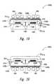
- FIG. 13is a cross-sectional view illustrating a packaged microelectronic device in accordance with yet another embodiment of the invention.
- FIG. 14is a cross-sectional view illustrating an initial stage of a method for manufacturing a packaged microelectronic device in accordance with an embodiment of the invention.
- FIGS. 15A and 15Bare cross-sectional views illustrating packaged microelectronic devices and methods for manufacturing packaged microelectronic devices in subsequent stages after the initial stage of FIG. 14 in accordance with additional embodiments of the invention.
- FIG. 16is a bottom plan view of an interface substrate for packaging a microelectronic device in accordance with an embodiment of the invention.
- FIGS. 17A and 17Billustrate a method for packaging a microelectronic device and the packaged microelectronic device in accordance with an embodiment of the invention.
- FIG. 18illustrates a packaged microelectronic device in accordance with an embodiment of the invention.
- FIG. 19illustrates a packaged microelectronic device in accordance with another embodiment of the invention.
- FIG. 20illustrates a packaged microelectronic device in accordance with yet another embodiment of the invention.
- FIGS. 21A and 21Billustrate an embodiment of packaging a microelectronic device and a packaged microelectronic device in accordance with yet another embodiment of the invention.
- substrate interfaceany type of device for coupling a microelectronic die to a printed circuit board, another microelectronic die, or another type of device.
- substrate interfaceany type of device for coupling a microelectronic die to a printed circuit board, another microelectronic die, or another type of device.
- the second die 120can have an inner surface 122 , a second terminal array 123 having a plurality of second bond-pads or terminals 124 extending along the inner surface 122 , an outer surface 125 , and at least one second integrated circuit 126 (shown schematically).
- the terminal arrays 113 and 123can be center arrays (as shown), periphery arrays, or other configurations for connecting the integrated circuits 116 and 126 to other components.
- the terminal arrays 113 and 123are typically gold bumps or solder bumps that have a very fine pitch of 0.075 mm, but the terminal arrays 113 and 123 can be made from other materials and have other pitches.
- the interface member 130can have only the intermediate section 136 (i.e., a die section) and one of the first or second sections (i.e., a ball array section) for use in single-die and/or stacked-die configurations.
- the embodiments of the first and second sections 132 and 134 shown in FIGS. 1 and 2provide separate ball-pad arrays for distributing the fine-pitch, high-density terminals 114 and 124 to a larger pitch that can be attached to a printed circuit board or another microelectronic device.
- the first section 132can include a first contact surface 137 a (FIG. 1) for engaging the exterior surface 115 of the first die 110
- the second section 134can include a second contact surface 137 b (FIG. 2) for contacting the outer surface 125 of the second die 120
- the first section 132can also include a first access surface 138 a (FIG. 2) with a first ball-pad array 139 a
- the second section 134can include a second access surface 138 b (FIG. 1) with a second ball-pad array 139 b.
- the first and second ball-pad arrays 139 a and 139 bcan have a plurality of ball-pads 143 that are connected to the first contacts 142 a of the first contact array 140 a and/or the second contacts 142 b of the second contact array 140 b by interconnecting circuitry 144 .
- the first and second ball-pad arrays 139 a and 139 bcan be identical or they can have different configurations. In one embodiment, for example, the first and second ball-pad arrays 139 a and 139 b are identical arrays in which all of the contacts 142 a and 142 b on the intermediate section 136 are connected to the same respective ball-pads 143 on both the first and second ball-pad arrays 139 a and 139 b.
- the ball-pad arrays 139 a and 139 bcan further include additional ball-pads for electrically coupling one stacked-die assembly onto another to form a multiple stacked-die assembly.
- the first contacts 142 acan be coupled to only one of the first or second ball-pad arrays 139 a or 139 b, and the second contacts 142 b can be coupled to only the other one of the first or second ball-pad arrays 139 a or 139 b.
- one portion of the first contacts 142 acan be coupled to the first ball-pad array 139 a and another portion of the first contacts 142 a can be coupled to the second ball-pad array 139 b.
- the ball-pad arrays 139 a and 139 bcan accordingly have several different configurations.
- FIGS. 3A-3Ccare side elevation views illustrating an embodiment of a process for manufacturing the stacked-die assembly 100 shown in FIGS. 1 and 2.
- the reference numbers in FIGS. 3A-3Ccorrespond to the reference numbers in FIGS. 1 and 2, and thus like reference numbers refer to like components in FIGS. 1-3C.
- the first and second dies 110 and 120are aligned with the intermediate section 136 of the interface substrate 130 such that the first terminal array 113 of the first die 110 is superimposed over the first contact array 140 a, and the second terminal array 123 of the second die 120 is aligned with the second contact array 140 b.
- the first and second dies 110 and 120are adhered to the intermediate section 136 of the interface substrate 130 .
- the first and second dies 110 and 120can be adhered to the intermediate section 136 using a flowable underfill, anisotropic conductive films, anisotropic conductive pastes, thermal compression techniques, thermalsonic techniques, no-flow underfill techniques, or other techniques that are known to persons skilled in the art.
- the first section 132 of the interface substrate 130is folded up (arrow A) to engage the first contact surface 137 a with the exterior surface 115 of the first die 110 .
- the second section 134 of the interface substrate 130is folded down (arrow B) so that the second contact surface 137 b engages the outer surface 125 of the second die 120 .
- the first and second contact surfaces 137 a and 137 b of the interface substrate 130are generally adhered to the first and second dies 110 and 120 by an adhesive 145 . Once the first and second sections 132 and 134 of the interface substrate 130 are adhered to the first and second dies 110 and 120 , the stacked-die assembly 100 is ready for testing and receiving solder balls on the ball-pads 143 .
- the embodiment of the stacked-die assembly 100 shown in FIGS. 1-3Cis expected to reduce capital expenditures and operating costs for testing stacked-die assemblies.
- One feature of several embodiments of the stacked-die assembly 100is that all of the terminals in the first and second terminal arrays 113 and 123 of the first and second dies 110 and 120 can be coupled to the ball-pads 143 of the first ball-pad array 139 a and/or the second ball-pad array 139 b.
- both of the first and second dies 110 and 120can be tested in a single test handler using the same test sockets, the same burn-in board, the same test program, and the same test procedure.
- the dies 110 and 120can be tested with the same test handler even when the first die 110 is a different type of die than the second die 120 .
- the stacked-die assembly 100 shown in FIGS. 1-3Care also expected to simplify the packaging process for creating stacked-die assemblies.
- the first and second ball-pad arrays 139 a and 139 bare identical arrays in which all of the terminals in both the first terminal array 113 of the first die 110 and the second terminal array 123 of the second die 120 are coupled to corresponding ball-pads 143 in each array 139 a and 139 b
- the only process step that needs to be customized for a specific stacked-die assemblyis the pattern of solder balls placed on the ball-pad arrays 139 a and/or 139 b at the end of the assembly/testing procedure. Therefore, the interface substrate 130 simplifies the process of fabricating stacked-die assemblies.
- stacked-die assembly 100are also expected to reduce the cost of manufacturing interface substrates.
- an individual interface substratemust be designed and manufactured for each type of die in a stacked-die assembly.
- a single mask and tooling systemis required for fabricating the interface substrate 130 . Therefore, several embodiments of the stacked-die assembly 100 are expected to reduce the cost of assembling microelectronic devices.
- FIG. 4is a side elevation view of another embodiment of the stacked-die assembly 100 .
- the ball-pads 143 on the first access surface 138 a of the first section 132are covered with an insulation layer 150 .
- a plurality of solder balls 160are deposited onto individual ball-pads 143 of the second ball-pad array 139 b.
- the solder balls 160are generally distributed in a pattern to couple the terminals of the first and second terminal arrays 113 and 123 to appropriate points on a printed circuit board or another type of component.
- FIG 5is a side elevation view of a multiple stacked-die assembly 500 in accordance with another embodiment of the invention.
- the multiple stacked-die assembly 500includes a plurality of individual stacked-die assemblies 100 a - 100 c.
- Each of the individual stacked-die assemblies 100 a - 100 ccan be the same as the stacked-die assembly 100 described above with reference to FIGS. 1-3C.
- a plurality of solder balls 160are deposited onto the ball-pads 143 of the second ball-pad array 139 b of each of the stacked-die assemblies 100 a - 100 c.
- the second stacked-die assembly 100 bis coupled to the first stacked-die assembly 100 a by contacting the solder balls 160 on the second ball-pad array 139 b of the second stacked-die assembly 100 b with selected ball-pads 143 of the first ball-pad array 139 a of the first stacked-die assembly 100 a.
- the third stacked-die assembly 100 ccan be similarly coupled to the second stacked-die assembly 100 b.
- the multiple stacked-die assembly 500can have any number of individual stacked-die assemblies 100 , and it is not necessarily limited to having three stacked-die assemblies. For example, the multiple stacked-die assembly 500 can have two or more individual stacked-die assemblies.
- the multiple stacked-die assembly 500 illustrated in FIG. 5provides a significant increase in the configurations of stacked microelectronic devices.
- all of the individual diescan be the same type of microelectronic device to significantly increase the capacity of a component without occupying a greater surface area on the printed circuit board.
- the microelectronic devicesfor example, can all be SRAM or DRAM devices to increase the memory capacity of a component.
- the multiple stacked-die assembly 500significantly increases the number of functions of a component because many different types of devices can be mounted onto the same surface area of a printed circuit board.
- the first stacked-die assembly 100 a of the multiple stacked-die assembly 500 in FIG. 5can be mounted to a printed circuit board to couple all of the stacked-die assemblies 100 a - 100 c to the printed circuit board.
- the first ball-pad array 139 a of the first stacked-die assembly 100 ahas ball-pads 143 that are configured to contact the solder balls 160 depending from the ball-pads 143 on the second ball-pad array 139 b of the second stacked-die assembly 100 b.
- the interface substrate 130 of the first stacked-die assembly 100 acan accordingly have interconnecting circuitry 144 with a pass-through circuit to couple the ball-pads 143 on the first ball-pad array 139 a of the first stacked-die assembly 100 a that contact the solder balls 160 depending from the second ball-pad array 139 b of the second stacked-die assembly 100 b with the desired ball-pads 143 on the second ball-pad array 139 b of the first stacked-die assembly 100 a.
- Such a pass-through circuitallows the interface substrate 130 of the first stacked-die assembly 100 a to be a conduit for the second stacked-die assembly 100 b.
- the interface substrate 130 of each of the first and second stacked-die assemblies 100 a and 100 bcan also be configured with pass-through circuits that coupled the third stacked-die assembly 100 c to a printed circuit board via the first and second stacked-die assemblies 100 a and 100 b.
- FIG. 6is a elevation view of another stacked-die assembly 600 in accordance with another embodiment of the invention.
- the stacked-die assembly 600includes a first die 110 , a second die 120 , and an interface substrate 630 attached to the first and second dies 110 and 120 .
- the first and second dies 110 and 120can be similar to those described above with respect to FIGS. 1-3C, and thus like reference numbers refer to like parts in FIGS. 1-3C and 6 .
- the interior surface of the first die 110 in the stacked-die assembly 600is bonded to the inner surface of the second die 120 by an adhesive 645 .
- the first terminal array 113is accordingly on the exterior surface of the first die 110
- the second terminal array 123is on the outer surface of the second die 120 .
- the first and second terminal arrays 113 and 123face outwardly away from each other in the stacked-die assembly 600 .
- the interface substrate 630has a body with a first section 632 , a second section 634 , and an intermediate section 636 between the first and second sections 632 and 634 .
- FIG. 7is a top isometric view of the interface substrate 630 of the stacked-die assembly 600 shown in FIG. 6 .
- the first section 632 of the interface substrate 630can have a first contact surface 637 a, a first access surface 638 a, a first ball-pad array 639 a including a plurality of ball-pads 643 on the first access surface 638 a, and a first contact array 640 a on the first contact surface 637 a.
- the second section 634 of the interface substrate 630can similarly include a second contact surface 637 b, a second access surface 638 b, a second ball-pad array 639 b including a plurality of ball-pads 643 on the second access surface 638 b, and a second contact array 640 b on the second contact surface 637 b.
- the first contact array 640 aengages the first terminal array 113 of the first die 110
- the second contact array 640 bengages the second terminal array 123 of the second die 120 .
- the first and second contact arrays 640 a and 640 bcan be electrically coupled to the ball-pads 643 of the first ball-pad array 639 a and/or the second ball-pad array 639 a by interconnecting circuitry 644 (shown schematically) in or on the interface substrate 630 . It will be appreciated that the first and second contact arrays 640 a and 640 b, and the first and second ball-pad arrays 639 a and 639 a, can have the same configurations as described above with respect to FIGS. 1-5.
- FIG. 8is a side elevation view of another embodiment of the stacked-die assembly 600 in which the interface substrate 630 has only one ball-pad array 139 on the second section 134 .
- the single ball-pad array 139 shown in this embodimentcan alternatively be on the first section 132 depending upon the particular application for the stacked-die assembly 600 .
- the interconnecting circuitry 644accordingly couples both the first and second contact arrays 640 a and 640 b to the ball-pad array 139 on either the first or the second sections 132 or 134 .
- This embodiment of the stacked-die assembly 600is particularly well suited for being a sole stacked-die assembly or the top stacked-die assembly of a multiple stacked-die assembly because the section of the interface substrate that does not have a ball-pad array electrically insulates the assembly without requiring a separate insulation layer.
- FIG. 9is an exploded isometric view showing a microelectronic device 900 including a microelectronic die 910 and an interface substrate or redistribution member 930 in accordance with another embodiment of the invention.
- the die 910can have an active side 912 , an inactive side 914 (i.e., backside), and a plurality of bond-pads 916 on the active side 912 .
- the die 910can also include integrated circuitry 918 that is coupled to at least a number of the bond-pads 916 to provide the desired electrical connections to the integrated circuitry 918 .
- Many features of the die 910 and the redistribution member 930are similar to the die 110 and the interface substrate 130 described above, and related or like components are generally identified by like terms.
- the redistribution member 930can have a body 932 composed of a material that can be flexed at room temperature or at elevated temperatures.
- the body 932 of the redistribution member 930can be a thin, flexible material that bends merely under the influence of gravity or a slight force. Suitable materials for the body 932 include tapes or other substrates, such as polyimides and other materials as set forth above with respect to the interface substrate 130 .
- the body 932can include a first section or die section 934 and a second section or array section 936 .
- the area between the die section 934 and the array section 936can define an intermediate section 938 , but it will appreciated that the intermediate section 938 can merely be a contiguous part of either one of the die section 934 and/or the array section 936 .
- the die section 934can include a slot 939 and a plurality of contacts 940 arranged in a terminal array adjacent to the slot 939 .
- the array section 936can include a plurality of ball-pads 942 arranged in a ball-pad array.
- the contacts 940can be coupled to selected ball-pads 942 by interconnecting circuitry 950 that is in or on the body 932 . Additionally, certain ball-pads 942 can be coupled to other ball-pads in the ball-pad array by other interconnecting circuitry 950 a in the body 932 .
- the die 910is attached to the die section 934 of the redistribution member 930 , and then the array section 936 of the redistribution member 932 is folded (arrow F) to position the array section 936 across from the die section 934 with either the die 910 or a casing between the array section 936 and the die section 934 .
- FIGS. 10A-10Cillustrate various stages of packaging the microelectronic device 900 in accordance with one embodiment of the invention.
- the die 910is attached to the redistribution member 930 with strips of adhesive 920 along the slot 939 on the back side of the die section 934 .
- the bond-pads 916 on the die 910are then electrically coupled to the contacts 940 on the redistribution member 930 by individual wire bonds 960 .
- the wire-bonds 960can be gold bonds or other types of materials that are known in the art.
- the die section 934does not include the slot 939 , but rather has a plurality of contacts on the side of the body 932 opposite of the ball-pads 942 .
- the bond-pads 916 on the die 910can be flip-chip mounted to such contacts on the opposite side of the body in a manner similar to the contact between the bond-pads 114 and the contacts 142 a described above with reference to FIG. 1 .
- the casing 970can include a first cover 972 a adjacent to the side of the die 910 and a second cover 972 b that covers the bond-pads 916 , the contacts 940 , and the wire-bonds 960 .
- the casing 970can be molded using a molding compound and techniques known in the art.
- an adhesive 980can be applied to the inactive side 914 of the die 910 and the array section 936 of the redistribution member 930 can be folded (arrow F) to position the back side of the second section 936 against the adhesive 980 .
- FIG. 10Cillustrates the packaged microelectronic device 900 after the array section 936 of the redistribution member 930 has been folded on to the adhesive 980 on the inactive side 914 of the die 910 .
- the intermediate section 938extends around at least a portion of a side surface of the casing 970 , and the array section 936 is spaced across from the die section 934 .
- a plurality of conductive/connective balls 990such as solder balls, can then be deposited onto the ball-pads 942 for coupling the packaged microelectronic device 900 to another device (e.g., a printed circuit board, another packaged microelectronic device for stacking, or other components).
- FIG. 11is a cross-sectional view illustrating another embodiment of the microelectronic device 900 .
- the inactive surface 914 at the die 910remains exposed.
- the ball-pads 942 on the array section 936 of the redistribution member 930are accordingly on the opposite side of the redistribution member shown in FIGS. 10A-10C.
- the array section 936is folded downward in this embodiment such that the interconnecting section 938 extends around the side of the second cover 972 b and is adhered to an exterior face 974 of the casing 970 by an adhesive 980 .
- the embodiment of the packaged device 900 in FIG. 11is similar to the embodiment shown in FIG. 10C, except that the ball-pads 942 face in the opposite direction. In both embodiments, the array section 936 is spaced across from the die section 934 .
- FIGS. 12 and 13are cross-sectional views illustrating additional embodiments of the microelectronic device 900 in accordance with other aspects of the invention.
- the first cover 972 a of the casing 970completely encloses the inactive side 914 of the die 910 .
- the array section 936is attached to the second cover 972 b by an adhesive 980 .
- the array section 936is attached to the first cover 972 a of the casing.
- a number of solder balls or other types of connectors 990can be deposited on to the ball-pads 942 .
- FIGS. 14, 15 A and 15 Billustrate yet additional embodiments of the microelectronic device 900 .
- the microelectronic device 900is the same as the device shown in FIG. 12, but the ball-pads 942 in FIG. 14 are true via ball-pads that extend completely through the body 932 of the redistribution member 930 .
- the array section 936can be positioned on either the second cover 972 b (FIG. 15A) or the first cover 972 a in a manner similar to that explained above with reference to FIGS. 12 and 13.
- FIG. 16is a bottom plan view of a redistribution member 1030 for use in a packaged microelectronic device in accordance with another embodiment of the invention.
- the redistribution member 1030can include a body 1032 having a die section 1034 , a first array section 1036 a, and a second array section 1036 b.
- the redistribution member 1030also includes a slot 1039 for a board-on-chip configuration similar to the embodiment of the microelectronic device 900 with the slot 939 described above with reference to FIGS. 9-15B.
- the redistribution member 1030can also include a first ball-pad array 1041 a having a plurality of first ball-pads 1042 a, a second ball-pad array 1041 b having a plurality of second ball-pads 1042 b, and a plurality of contacts 1040 adjacent to the slot 1039 .
- the ball-pads 1042 a-bcan be coupled to corresponding contacts 1040 and/or other ball-pads 1042 a-b by interconnecting circuitry in the body 1032 .
- the materials of the redistribution member 1030can be similar to those described above with reference to redistribution member 930 .
- FIGS. 17A and 17Bare cross-sectional views of an embodiment of a microelectronic device 1000 using an embodiment of the redistribution member 1030 .
- the die 910is attached the redistribution member 1030 by strips of an adhesive 920 and the bond-pads 916 are coupled to the contacts 1040 using wire-bonds 1060 that pass through the slot 1039 .
- the bond-pads 916 , the wire-bonds 1060 , the contacts 1040 , and at least a portion of the die 910are then encapsulated by the casing 970 .
- the first and second array sections 1036 a-bare then folded upward (arrow F).
- FIG. 17Billustrates the packaged microelectronic die 1000 after the first array section 1036 a has been adhered to one side of the die 910 and the second array section 1036 b has been adhered to another side of the die 910 .
- the first and second array sections 1036 a-bcan be adhered to the die 910 by an adhesive 980 as explained above.
- the redistribution member 1030accordingly has a first interconnecting section 1038 a extending around one side of the casing 970 and a second interconnecting member 1038 b extending around another side of the casing 970 .
- FIGS. 18-20illustrate additional embodiments of packaged microelectronic devices in accordance with additional embodiments of the invention.
- the packaged devices 1000 a-c shown in FIGS. 18-20, respectively,are similar to the packaged microelectronic device 1000 shown in FIGS. 17A and 17B, and thus like reference members refer to like components throughout these figures.
- FIG. 18illustrates a packaged microelectronic device 1000 a in which the inactive side 914 of the die 910 is exposed, and the first and second array sections 1036 a-b are attached to the second cover 972 b of the casing 970 .
- FIG. 19illustrates a microelectronic device 1000 b in which the die 910 is completely encapsulated, and the first and second array sections 1036 a-b are attached to the top of the first cover 972 a.
- FIG. 20illustrates a microelectronic device 1000 c that is similar to the microelectronic device 1000 b shown in FIG. 19, but the first and second array sections 1036 a-b are attached to the second cover 972 b.
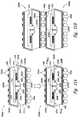
- FIGS. 21A and 21Billustrate a stacked die assembly comprising separate packaged microelectronic devices 2000 a and 2000 b.
- the first package microelectronic device 2000 acan include a die 910 , a casing 970 having a first cover 972 a and a second cover 972 b, and a redistribution member 2030 attached to the active side 912 of the die 910 . A portion of the redistribution member 2030 is also sandwiched between the first and second covers 972 a-b.
- the second microelectronic device 2000 bcan have components that are identical to the first microelectronic device 2000 a.
- the first and second microelectronic devices 2000 a-bcan be different types of dies, especially if they are not mirror components.
- Each of the redistribution members 2030can include a die section 2034 , first and second array sections 2036 a and 2036 b, and first and second interconnecting sections 2038 a and 2038 b.
- the first interconnecting section 2038 acan extend from one side of the die section 2034 and around a side portion of the first cover 972 a
- the first array section 2036 acan extend from the first interconnecting section 2038 a and be adhered to an exterior face of the first cover 972 a.
- the second interconnecting section 2038 bcan extend around a side portion of the second cover 972 b
- the second array section 2036 bcan extend from the second interconnecting section 2038 b and be adhered to an exterior face of the second cover 972 b.
- the die section 2034can have a plurality of contacts 2040 that can be coupled to the bond-pads 916 on the die 910 .
- the first array section 2036 acan include a plurality of first ball-pads 2042 a
- the second array section 2036 bcan include a plurality of second ball-pads 2042 b.
- Each redistribution member 2030can further include interconnecting circuitry (not shown in FIGS. 21 A and 21 B).
- the interconnecting circuitrycan (a) couple the contacts 2040 to selected first and/or second ball-pads 2042 a-b, and/or (b) couple a number of the first ball-pads 2042 a to the second ball-pads 2042 b.
- FIG. 21Billustrates the first and second microelectronic devices 2000 a-b in a stacked configuration.
- a plurality of first connectors 990 a attached to the second ball-pads 2042 b of the first microelectronic device 2000 aare mounted to the first ball-pads 2042 a of the second microelectronic device 2000 b.
- a plurality of second connectors 900 b projecting from the second array section 2036 b of the second microelectronic device 2000 bcan be coupled to yet another packaged microelectronic device for further packaging, a printed circuit board assembly, or another type of component.
- FIGS. 9-21Bare expected to provide several of the same advantages as described above with reference to FIGS. 1-8.
- many of the embodiments shown and described aboveneed only a single type of testing socket to test different types of devices, and manufacturers need only supply a single type of interposer substrate.
- Thisis possible because many embodiments of the invention use a single type of interface substrate or redistribution member that can be used in different applications with different types of dies.
- several embodimentsare expected to provide large ball-pad arrays in a small footprint because the redistribution member is flexible and folded over so that the ball-pad array is superimposed relative to the die.
- a moldcan clamp on the intermediate sections of a redistribution member for encapsulation, and then the redistribution member can be folded so that the ball-grid array is over or under the die.
- the microelectronic devicesaccordingly can have a large ball-pad array with a small footprint for mounting high-performance devices in small spaces.
Landscapes
- Engineering & Computer Science (AREA)
- Microelectronics & Electronic Packaging (AREA)
- Power Engineering (AREA)
- Computer Hardware Design (AREA)
- Physics & Mathematics (AREA)
- Condensed Matter Physics & Semiconductors (AREA)
- General Physics & Mathematics (AREA)
- Encapsulation Of And Coatings For Semiconductor Or Solid State Devices (AREA)
- Semiconductor Memories (AREA)
Abstract
Description
Claims (4)
Priority Applications (1)
| Application Number | Priority Date | Filing Date | Title |
|---|---|---|---|
| US09/944,723US6560117B2 (en) | 2000-06-28 | 2001-08-30 | Packaged microelectronic die assemblies and methods of manufacture |
Applications Claiming Priority (2)
| Application Number | Priority Date | Filing Date | Title |
|---|---|---|---|
| US09/606,432US6552910B1 (en) | 2000-06-28 | 2000-06-28 | Stacked-die assemblies with a plurality of microelectronic devices and methods of manufacture |
| US09/944,723US6560117B2 (en) | 2000-06-28 | 2001-08-30 | Packaged microelectronic die assemblies and methods of manufacture |
Related Parent Applications (1)
| Application Number | Title | Priority Date | Filing Date |
|---|---|---|---|
| US09/606,432Continuation-In-PartUS6552910B1 (en) | 2000-06-28 | 2000-06-28 | Stacked-die assemblies with a plurality of microelectronic devices and methods of manufacture |
Publications (2)
| Publication Number | Publication Date |
|---|---|
| US20020030975A1 US20020030975A1 (en) | 2002-03-14 |
| US6560117B2true US6560117B2 (en) | 2003-05-06 |
Family
ID=46278080
Family Applications (1)
| Application Number | Title | Priority Date | Filing Date |
|---|---|---|---|
| US09/944,723Expired - LifetimeUS6560117B2 (en) | 2000-06-28 | 2001-08-30 | Packaged microelectronic die assemblies and methods of manufacture |
Country Status (1)
| Country | Link |
|---|---|
| US (1) | US6560117B2 (en) |
Cited By (166)
| Publication number | Priority date | Publication date | Assignee | Title |
|---|---|---|---|---|
| US20030081392A1 (en)* | 2001-10-26 | 2003-05-01 | Staktek Group, L.P. | Integrated circuit stacking system and method |
| US20030111736A1 (en)* | 2001-12-14 | 2003-06-19 | Roeters Glen E. | Csp chip stack with flex circuit |
| US20030234443A1 (en)* | 2001-10-26 | 2003-12-25 | Staktek Group, L.P. | Low profile stacking system and method |
| US20040000708A1 (en)* | 2001-10-26 | 2004-01-01 | Staktek Group, L.P. | Memory expansion and chip scale stacking system and method |
| US20040038449A1 (en)* | 2000-08-23 | 2004-02-26 | Corisis David J. | Stacked microelectronic dies and methods for stacking microelectronic dies |
| US20040052060A1 (en)* | 2001-10-26 | 2004-03-18 | Staktek Group, L.P. | Low profile chip scale stacking system and method |
| US20040178495A1 (en)* | 2003-03-14 | 2004-09-16 | Yean Tay Wuu | Microelectronic devices and methods for packaging microelectronic devices |
| US20040183183A1 (en)* | 2001-10-26 | 2004-09-23 | Staktek Group, L.P. | Integrated circuit stacking system and method |
| US20040188820A1 (en)* | 2002-08-21 | 2004-09-30 | Corisis David J | Packaged microelectronic devices and methods for assembling microelectronic devices |
| US20040229401A1 (en)* | 2003-05-12 | 2004-11-18 | Bolken Todd O. | Method for fabricating semiconductor component having stacked, encapsulated dice |
| US20050012185A1 (en)* | 2003-03-04 | 2005-01-20 | Peng Neo Chee | Microelectronic component assemblies employing lead frames having reduced-thickness inner lengths |
| US20050019984A1 (en)* | 2000-08-09 | 2005-01-27 | Tongbi Jiang | Multiple substrate microelectronic devices and methods of manufacture |
| US20050026415A1 (en)* | 2002-01-16 | 2005-02-03 | Micron Technology, Inc. | Fabrication of stacked microelectronic devices |
| US20050045378A1 (en)* | 2003-08-29 | 2005-03-03 | Heng Mung Suan | Stacked microfeature devices and associated methods |
| US20050056921A1 (en)* | 2003-09-15 | 2005-03-17 | Staktek Group L.P. | Stacked module systems and methods |
| US20050057911A1 (en)* | 2003-09-15 | 2005-03-17 | Staktek Group, L.P. | Memory expansion and integrated circuit stacking system and method |
| US20050104228A1 (en)* | 2003-11-13 | 2005-05-19 | Rigg Sidney B. | Microelectronic devices, methods for forming vias in microelectronic devices, and methods for packaging microelectronic devices |
| US20050104171A1 (en)* | 2003-11-13 | 2005-05-19 | Benson Peter A. | Microelectronic devices having conductive complementary structures and methods of manufacturing microelectronic devices having conductive complementary structures |
| US20050127478A1 (en)* | 2003-12-10 | 2005-06-16 | Hiatt William M. | Microelectronic devices and methods for filling vias in microelectronic devices |
| US20050173805A1 (en)* | 2003-12-30 | 2005-08-11 | Tessera, Inc. | Micro pin grid array with pin motion isolation |
| US20050181655A1 (en)* | 2003-12-30 | 2005-08-18 | Tessera, Inc. | Micro pin grid array with wiping action |
| US20050181544A1 (en)* | 2003-12-30 | 2005-08-18 | Tessera, Inc. | Microelectronic packages and methods therefor |
| US20050194674A1 (en)* | 2004-03-02 | 2005-09-08 | Jochen Thomas | Integrated circuit with re-route layer and stacked die assembly |
| US20050194672A1 (en)* | 2003-11-04 | 2005-09-08 | Tessera, Inc. | Stacked packages and systems incorporating the same |
| US20050227409A1 (en)* | 2004-04-13 | 2005-10-13 | Taiwan Semiconductor Manufacturing Co., Ltd. | Microelectronics package assembly tool and method of manufacture therewith |
| US20050277279A1 (en)* | 2004-06-14 | 2005-12-15 | Shijian Luo | Microfeature devices and methods for manufacturing microfeature devices |
| US20050284658A1 (en)* | 2003-10-06 | 2005-12-29 | Tessera, Inc. | Components with posts and pads |
| US20060022338A1 (en)* | 2002-08-22 | 2006-02-02 | Infineon Technologies Ag | Semiconductor component having a CSP housing |
| US7003362B2 (en) | 2004-05-11 | 2006-02-21 | Taiwan Semiconductor Manufacturing Company, Ltd. | System and method for customized tape-out requests for integrated circuit manufacturing |
| US20060044773A1 (en)* | 2004-08-25 | 2006-03-02 | Micron Technology, Inc. | Methods and apparatuses for transferring heat from stacked microfeature devices |
| US20060043534A1 (en)* | 2004-08-26 | 2006-03-02 | Kirby Kyle K | Microfeature dies with porous regions, and associated methods and systems |
| US20060053345A1 (en)* | 2004-09-03 | 2006-03-09 | Staktek Group L.P. | Thin module system and method |
| US7033861B1 (en) | 2005-05-18 | 2006-04-25 | Staktek Group L.P. | Stacked module systems and method |
| US20060090102A1 (en)* | 2004-09-03 | 2006-04-27 | Wehrly James D Jr | Circuit module with thermal casing systems and methods |
| US7037756B1 (en) | 2001-08-30 | 2006-05-02 | Micron Technology, Inc. | Stacked microelectronic devices and methods of fabricating same |
| US7053478B2 (en) | 2001-10-26 | 2006-05-30 | Staktek Group L.P. | Pitch change and chip scale stacking system |
| US20060157842A1 (en)* | 2005-01-20 | 2006-07-20 | Staktek Group L.P. | Inverted CSP stacking system and method |
| US20060177970A1 (en)* | 2005-02-08 | 2006-08-10 | Micron Technology, Inc. | Methods of Adhering Microfeature Workpieces, Including A Chip, To A Support Member |
| US20060249857A1 (en)* | 2005-03-16 | 2006-11-09 | Tessera, Inc. | Microelectronic packages and methods therefor |
| US20060292858A1 (en)* | 2002-07-18 | 2006-12-28 | Micron Technology, Inc. | Techniques to create low K ILD for beol |
| US20070020811A1 (en)* | 2002-04-04 | 2007-01-25 | Micron Technology, Inc. | Method and apparatus for attaching microelectronic substrates and support members |
| US20070045807A1 (en)* | 2005-09-01 | 2007-03-01 | Micron Technology, Inc. | Microelectronic devices and methods for manufacturing microelectronic devices |
| US20070045862A1 (en)* | 2005-09-01 | 2007-03-01 | Micron Technology, Inc. | Stacked microelectronic devices and methods for manufacturing microelectronic devices |
| US20070045875A1 (en)* | 2005-08-30 | 2007-03-01 | Micron Technology, Inc. | Methods for wafer-level packaging of microfeature devices and microfeature devices formed using such methods |
| US20070045803A1 (en)* | 2005-08-26 | 2007-03-01 | Micron Technology, Inc. | Microelectronic device packages, stacked microelectronic device packages, and methods for manufacturing microelectronic devices |
| US20070045812A1 (en)* | 2005-08-31 | 2007-03-01 | Micron Technology, Inc. | Microfeature assemblies including interconnect structures and methods for forming such interconnect structures |
| US20070045796A1 (en)* | 2005-08-19 | 2007-03-01 | Micron Technology, Inc. | Microelectronic devices, stacked microelectronic devices, and methods for manufacturing microelectronic devices |
| US20070045797A1 (en)* | 2005-08-24 | 2007-03-01 | Micron Technology, Inc. | Microelectronic devices and microelectronic support devices, and associated assemblies and methods |
| US7198693B1 (en) | 2002-02-20 | 2007-04-03 | Micron Technology, Inc. | Microelectronic device having a plurality of stacked dies and methods for manufacturing such microelectronic assemblies |
| US7202555B2 (en) | 2001-10-26 | 2007-04-10 | Staktek Group L.P. | Pitch change and chip scale stacking system and method |
| USRE39628E1 (en) | 1999-05-05 | 2007-05-15 | Stakick Group, L.P. | Stackable flex circuit IC package and method of making same |
| US20070148820A1 (en)* | 2005-12-22 | 2007-06-28 | Micron Technology, Inc. | Microelectronic devices and methods for manufacturing microelectronic devices |
| US20070148822A1 (en)* | 2005-12-23 | 2007-06-28 | Tessera, Inc. | Microelectronic packages and methods therefor |
| US20070148819A1 (en)* | 2005-12-23 | 2007-06-28 | Tessera, Inc. | Microelectronic assemblies having very fine pitch stacking |
| US20070155048A1 (en)* | 2005-12-29 | 2007-07-05 | Micron Technology, Inc. | Methods for packaging microelectronic devices and microelectronic devices formed using such methods |
| US20070181989A1 (en)* | 2006-02-08 | 2007-08-09 | Micron Technology, Inc. | Microelectronic devices, stacked microelectronic devices, and methods for manufacturing such devices |
| US20070210441A1 (en)* | 2006-03-08 | 2007-09-13 | Micron Technology, Inc. | Microelectronic device assemblies including assemblies with recurved leadframes, and associated methods |
| US20070228577A1 (en)* | 2006-03-29 | 2007-10-04 | Micron Technology, Inc. | Packaged microelectronic devices recessed in support member cavities, and associated methods |
| US7289327B2 (en) | 2006-02-27 | 2007-10-30 | Stakick Group L.P. | Active cooling methods and apparatus for modules |
| US20070262436A1 (en)* | 2006-05-12 | 2007-11-15 | Micron Technology, Inc. | Microelectronic devices and methods for manufacturing microelectronic devices |
| US7304382B2 (en) | 2006-01-11 | 2007-12-04 | Staktek Group L.P. | Managed memory component |
| US7310458B2 (en) | 2001-10-26 | 2007-12-18 | Staktek Group L.P. | Stacked module systems and methods |
| US20070298585A1 (en)* | 2006-06-22 | 2007-12-27 | Applied Materials, Inc. | Dielectric deposition and etch back processes for bottom up gapfill |
| US20080003402A1 (en)* | 2003-10-06 | 2008-01-03 | Tessera, Inc. | Fine pitch microcontacts and method for forming thereof |
| US20080009096A1 (en)* | 2006-07-10 | 2008-01-10 | Samsung Electronics Co., Ltd. | Package-on-package and method of fabricating the same |
| US20080006940A1 (en)* | 2006-07-05 | 2008-01-10 | Micron Technology, Inc. | Lead frames, microelectronic devices with lead frames, and methods for manufacturing lead frames and microelectronic devices with lead frames |
| US20080012110A1 (en)* | 2006-07-17 | 2008-01-17 | Micron Technology, Inc. | Microelectronic packages with leadframes, including leadframes configured for stacked die packages, and associated systems and methods |
| US7324352B2 (en) | 2004-09-03 | 2008-01-29 | Staktek Group L.P. | High capacity thin module system and method |
| US20080048316A1 (en)* | 2006-08-25 | 2008-02-28 | Micron Technology, Inc. | Packaged microdevices and methods for manufacturing packaged microdevices |
| US20080050901A1 (en)* | 2006-08-23 | 2008-02-28 | Micron Technology, Inc. | Packaged microelectronic devices and methods for manufacturing packaged microelectronic devices |
| US7365424B2 (en) | 2004-07-23 | 2008-04-29 | Micron Technology, Inc. | Microelectronic component assemblies with recessed wire bonds and methods of making same |
| US7371609B2 (en) | 2001-10-26 | 2008-05-13 | Staktek Group L.P. | Stacked module systems and methods |
| US20080128900A1 (en)* | 2006-12-04 | 2008-06-05 | Micron Technology, Inc. | Packaged microelectronic devices and methods for manufacturing packaged microelectronic devices |
| US7417310B2 (en) | 2006-11-02 | 2008-08-26 | Entorian Technologies, Lp | Circuit module having force resistant construction |
| US7423885B2 (en) | 2004-09-03 | 2008-09-09 | Entorian Technologies, Lp | Die module system |
| US20080224291A1 (en)* | 2007-03-13 | 2008-09-18 | Micron Technology, Inc. | Packaged semiconductor components having substantially rigid support members and methods of packaging semiconductor components |
| US7443023B2 (en) | 2004-09-03 | 2008-10-28 | Entorian Technologies, Lp | High capacity thin module system |
| US7462936B2 (en) | 2003-10-06 | 2008-12-09 | Tessera, Inc. | Formation of circuitry with modification of feature height |
| US7468553B2 (en) | 2006-10-20 | 2008-12-23 | Entorian Technologies, Lp | Stackable micropackages and stacked modules |
| US20080318348A1 (en)* | 2007-06-25 | 2008-12-25 | Spansion Llc | Method of constructing a stacked-die semiconductor structure |
| US7480152B2 (en) | 2004-09-03 | 2009-01-20 | Entorian Technologies, Lp | Thin module system and method |
| US20090026600A1 (en)* | 2007-07-24 | 2009-01-29 | Micron Technology, Inc. | Microelectronic die packages with metal leads, including metal leads for stacked die packages, and associated systems and methods |
| US7485951B2 (en)* | 2001-10-26 | 2009-02-03 | Entorian Technologies, Lp | Modularized die stacking system and method |
| US20090045489A1 (en)* | 2007-08-16 | 2009-02-19 | Micron Technology, Inc. | Microelectronic die packages with leadframes, including leadframe-based interposer for stacked die packages, and associated systems and methods |
| US7508069B2 (en) | 2006-01-11 | 2009-03-24 | Entorian Technologies, Lp | Managed memory component |
| US7508058B2 (en) | 2006-01-11 | 2009-03-24 | Entorian Technologies, Lp | Stacked integrated circuit module |
| US7511969B2 (en) | 2006-02-02 | 2009-03-31 | Entorian Technologies, Lp | Composite core circuit module system and method |
| US7511968B2 (en) | 2004-09-03 | 2009-03-31 | Entorian Technologies, Lp | Buffered thin module system and method |
| US7522421B2 (en) | 2004-09-03 | 2009-04-21 | Entorian Technologies, Lp | Split core circuit module |
| US7542297B2 (en) | 2004-09-03 | 2009-06-02 | Entorian Technologies, Lp | Optimized mounting area circuit module system and method |
| US7576995B2 (en) | 2005-11-04 | 2009-08-18 | Entorian Technologies, Lp | Flex circuit apparatus and method for adding capacitance while conserving circuit board surface area |
| US7579687B2 (en) | 2004-09-03 | 2009-08-25 | Entorian Technologies, Lp | Circuit module turbulence enhancement systems and methods |
| US7606049B2 (en) | 2004-09-03 | 2009-10-20 | Entorian Technologies, Lp | Module thermal management system and method |
| US7605454B2 (en) | 2006-01-11 | 2009-10-20 | Entorian Technologies, Lp | Memory card and method for devising |
| US7606040B2 (en) | 2004-09-03 | 2009-10-20 | Entorian Technologies, Lp | Memory module system and method |
| US7606050B2 (en) | 2004-09-03 | 2009-10-20 | Entorian Technologies, Lp | Compact module system and method |
| US7608920B2 (en) | 2006-01-11 | 2009-10-27 | Entorian Technologies, Lp | Memory card and method for devising |
| US7616452B2 (en) | 2004-09-03 | 2009-11-10 | Entorian Technologies, Lp | Flex circuit constructions for high capacity circuit module systems and methods |
| USRE41039E1 (en) | 2000-01-13 | 2009-12-15 | Entorian Technologies, Lp | Stackable chip package with flex carrier |
| US7656678B2 (en) | 2001-10-26 | 2010-02-02 | Entorian Technologies, Lp | Stacked module systems |
| US20100044860A1 (en)* | 2008-08-21 | 2010-02-25 | Tessera Interconnect Materials, Inc. | Microelectronic substrate or element having conductive pads and metal posts joined thereto using bond layer |
| US7719098B2 (en) | 2001-10-26 | 2010-05-18 | Entorian Technologies Lp | Stacked modules and method |
| US7745944B2 (en) | 2005-08-31 | 2010-06-29 | Micron Technology, Inc. | Microelectronic devices having intermediate contacts for connection to interposer substrates, and associated methods of packaging microelectronic devices with intermediate contacts |
| US7760513B2 (en) | 2004-09-03 | 2010-07-20 | Entorian Technologies Lp | Modified core for circuit module system and method |
| US20110149533A1 (en)* | 2009-12-22 | 2011-06-23 | Mxtran Inc. | Integrated circuit film for smart card |
| US8330272B2 (en) | 2010-07-08 | 2012-12-11 | Tessera, Inc. | Microelectronic packages with dual or multiple-etched flip-chip connectors |
| US8404520B1 (en) | 2011-10-17 | 2013-03-26 | Invensas Corporation | Package-on-package assembly with wire bond vias |
| US20130088671A1 (en)* | 2011-10-05 | 2013-04-11 | Paul S. Drzaic | Displays with Minimized Border Regions |
| US8482111B2 (en) | 2010-07-19 | 2013-07-09 | Tessera, Inc. | Stackable molded microelectronic packages |
| US8525314B2 (en) | 2004-11-03 | 2013-09-03 | Tessera, Inc. | Stacked packaging improvements |
| US8580607B2 (en) | 2010-07-27 | 2013-11-12 | Tessera, Inc. | Microelectronic packages with nanoparticle joining |
| US8623706B2 (en) | 2010-11-15 | 2014-01-07 | Tessera, Inc. | Microelectronic package with terminals on dielectric mass |
| US8835228B2 (en) | 2012-05-22 | 2014-09-16 | Invensas Corporation | Substrate-less stackable package with wire-bond interconnect |
| US8853558B2 (en) | 2010-12-10 | 2014-10-07 | Tessera, Inc. | Interconnect structure |
| US8872318B2 (en) | 2011-08-24 | 2014-10-28 | Tessera, Inc. | Through interposer wire bond using low CTE interposer with coarse slot apertures |
| US8878353B2 (en) | 2012-12-20 | 2014-11-04 | Invensas Corporation | Structure for microelectronic packaging with bond elements to encapsulation surface |
| US8883563B1 (en) | 2013-07-15 | 2014-11-11 | Invensas Corporation | Fabrication of microelectronic assemblies having stack terminals coupled by connectors extending through encapsulation |
| US8884448B2 (en) | 2007-09-28 | 2014-11-11 | Tessera, Inc. | Flip chip interconnection with double post |
| US8975738B2 (en) | 2012-11-12 | 2015-03-10 | Invensas Corporation | Structure for microelectronic packaging with terminals on dielectric mass |
| US9023691B2 (en) | 2013-07-15 | 2015-05-05 | Invensas Corporation | Microelectronic assemblies with stack terminals coupled by connectors extending through encapsulation |
| US9034696B2 (en) | 2013-07-15 | 2015-05-19 | Invensas Corporation | Microelectronic assemblies having reinforcing collars on connectors extending through encapsulation |
| US9082753B2 (en) | 2013-11-12 | 2015-07-14 | Invensas Corporation | Severing bond wire by kinking and twisting |
| US9087815B2 (en) | 2013-11-12 | 2015-07-21 | Invensas Corporation | Off substrate kinking of bond wire |
| US9093435B2 (en) | 2011-05-03 | 2015-07-28 | Tessera, Inc. | Package-on-package assembly with wire bonds to encapsulation surface |
| US9159708B2 (en) | 2010-07-19 | 2015-10-13 | Tessera, Inc. | Stackable molded microelectronic packages with area array unit connectors |
| US9165888B2 (en) | 2008-09-11 | 2015-10-20 | Micron Technology, Inc. | Interconnect structures for stacked dies, including penetrating structures for through-silicon vias, and associated systems and methods |
| US9214454B2 (en) | 2014-03-31 | 2015-12-15 | Invensas Corporation | Batch process fabrication of package-on-package microelectronic assemblies |
| US9224717B2 (en) | 2011-05-03 | 2015-12-29 | Tessera, Inc. | Package-on-package assembly with wire bonds to encapsulation surface |
| US9286826B2 (en) | 2011-10-28 | 2016-03-15 | Apple Inc. | Display with vias for concealed printed circuit and component attachment |
| US9324681B2 (en) | 2010-12-13 | 2016-04-26 | Tessera, Inc. | Pin attachment |
| US9349706B2 (en) | 2012-02-24 | 2016-05-24 | Invensas Corporation | Method for package-on-package assembly with wire bonds to encapsulation surface |
| US9391008B2 (en) | 2012-07-31 | 2016-07-12 | Invensas Corporation | Reconstituted wafer-level package DRAM |
| US9412714B2 (en) | 2014-05-30 | 2016-08-09 | Invensas Corporation | Wire bond support structure and microelectronic package including wire bonds therefrom |
| US9454025B2 (en) | 2012-08-31 | 2016-09-27 | Apple Inc. | Displays with reduced driver circuit ledges |
| US9502390B2 (en) | 2012-08-03 | 2016-11-22 | Invensas Corporation | BVA interposer |
| US9515131B2 (en) | 2012-08-17 | 2016-12-06 | Apple Inc. | Narrow border organic light-emitting diode display |
| US9583411B2 (en) | 2014-01-17 | 2017-02-28 | Invensas Corporation | Fine pitch BVA using reconstituted wafer with area array accessible for testing |
| US9601454B2 (en) | 2013-02-01 | 2017-03-21 | Invensas Corporation | Method of forming a component having wire bonds and a stiffening layer |
| US9633971B2 (en) | 2015-07-10 | 2017-04-25 | Invensas Corporation | Structures and methods for low temperature bonding using nanoparticles |
| US9646917B2 (en) | 2014-05-29 | 2017-05-09 | Invensas Corporation | Low CTE component with wire bond interconnects |
| US9659848B1 (en) | 2015-11-18 | 2017-05-23 | Invensas Corporation | Stiffened wires for offset BVA |
| US9685365B2 (en) | 2013-08-08 | 2017-06-20 | Invensas Corporation | Method of forming a wire bond having a free end |
| US9691679B2 (en) | 2012-02-24 | 2017-06-27 | Invensas Corporation | Method for package-on-package assembly with wire bonds to encapsulation surface |
| US9728527B2 (en) | 2013-11-22 | 2017-08-08 | Invensas Corporation | Multiple bond via arrays of different wire heights on a same substrate |
| US9735084B2 (en) | 2014-12-11 | 2017-08-15 | Invensas Corporation | Bond via array for thermal conductivity |
| US9761554B2 (en) | 2015-05-07 | 2017-09-12 | Invensas Corporation | Ball bonding metal wire bond wires to metal pads |
| US9812402B2 (en) | 2015-10-12 | 2017-11-07 | Invensas Corporation | Wire bond wires for interference shielding |
| US9842745B2 (en) | 2012-02-17 | 2017-12-12 | Invensas Corporation | Heat spreading substrate with embedded interconnects |
| US9852969B2 (en) | 2013-11-22 | 2017-12-26 | Invensas Corporation | Die stacks with one or more bond via arrays of wire bond wires and with one or more arrays of bump interconnects |
| US9888579B2 (en) | 2015-03-05 | 2018-02-06 | Invensas Corporation | Pressing of wire bond wire tips to provide bent-over tips |
| US9911718B2 (en) | 2015-11-17 | 2018-03-06 | Invensas Corporation | ‘RDL-First’ packaged microelectronic device for a package-on-package device |
| US9935075B2 (en) | 2016-07-29 | 2018-04-03 | Invensas Corporation | Wire bonding method and apparatus for electromagnetic interference shielding |
| US9974122B2 (en) | 2012-06-25 | 2018-05-15 | Apple Inc. | Displays with vias |
| US9984992B2 (en) | 2015-12-30 | 2018-05-29 | Invensas Corporation | Embedded wire bond wires for vertical integration with separate surface mount and wire bond mounting surfaces |
| US10008477B2 (en) | 2013-09-16 | 2018-06-26 | Invensas Corporation | Microelectronic element with bond elements to encapsulation surface |
| US10008469B2 (en) | 2015-04-30 | 2018-06-26 | Invensas Corporation | Wafer-level packaging using wire bond wires in place of a redistribution layer |
| US10026717B2 (en) | 2013-11-22 | 2018-07-17 | Invensas Corporation | Multiple bond via arrays of different wire heights on a same substrate |
| US10181457B2 (en) | 2015-10-26 | 2019-01-15 | Invensas Corporation | Microelectronic package for wafer-level chip scale packaging with fan-out |
| US10299368B2 (en) | 2016-12-21 | 2019-05-21 | Invensas Corporation | Surface integrated waveguides and circuit structures therefor |
| US10332854B2 (en) | 2015-10-23 | 2019-06-25 | Invensas Corporation | Anchoring structure of fine pitch bva |
| US10381326B2 (en) | 2014-05-28 | 2019-08-13 | Invensas Corporation | Structure and method for integrated circuits packaging with increased density |
| US10460958B2 (en) | 2013-08-07 | 2019-10-29 | Invensas Corporation | Method of manufacturing embedded packaging with preformed vias |
| US10490528B2 (en) | 2015-10-12 | 2019-11-26 | Invensas Corporation | Embedded wire bond wires |
| US10535626B2 (en) | 2015-07-10 | 2020-01-14 | Invensas Corporation | Structures and methods for low temperature bonding using nanoparticles |
| US11973056B2 (en) | 2016-10-27 | 2024-04-30 | Adeia Semiconductor Technologies Llc | Methods for low temperature bonding using nanoparticles |
| US12211809B2 (en) | 2020-12-30 | 2025-01-28 | Adeia Semiconductor Bonding Technologies Inc. | Structure with conductive feature and method of forming same |
Families Citing this family (22)
| Publication number | Priority date | Publication date | Assignee | Title |
|---|---|---|---|---|
| FI20012052A0 (en)* | 2001-10-23 | 2001-10-23 | Mika Matti Sippola | A method for manufacturing a multilayer structure |
| US6576992B1 (en)* | 2001-10-26 | 2003-06-10 | Staktek Group L.P. | Chip scale stacking system and method |
| US6600222B1 (en)* | 2002-07-17 | 2003-07-29 | Intel Corporation | Stacked microelectronic packages |
| JP4072505B2 (en)* | 2003-02-28 | 2008-04-09 | エルピーダメモリ株式会社 | Stacked semiconductor package |
| US7505862B2 (en)* | 2003-03-07 | 2009-03-17 | Salmon Technologies, Llc | Apparatus and method for testing electronic systems |
| KR100541393B1 (en)* | 2003-04-26 | 2006-01-10 | 삼성전자주식회사 | Multichip BA Package |
| US7408258B2 (en)* | 2003-08-20 | 2008-08-05 | Salmon Technologies, Llc | Interconnection circuit and electronic module utilizing same |
| US20050184376A1 (en)* | 2004-02-19 | 2005-08-25 | Salmon Peter C. | System in package |
| US20050255722A1 (en)* | 2004-05-07 | 2005-11-17 | Salmon Peter C | Micro blade assembly |
| US7427809B2 (en) | 2004-12-16 | 2008-09-23 | Salmon Technologies, Llc | Repairable three-dimensional semiconductor subsystem |
| US20070007983A1 (en)* | 2005-01-06 | 2007-01-11 | Salmon Peter C | Semiconductor wafer tester |
| US20070023923A1 (en)* | 2005-08-01 | 2007-02-01 | Salmon Peter C | Flip chip interface including a mixed array of heat bumps and signal bumps |
| US20070023889A1 (en)* | 2005-08-01 | 2007-02-01 | Salmon Peter C | Copper substrate with feedthroughs and interconnection circuits |
| US20070023904A1 (en)* | 2005-08-01 | 2007-02-01 | Salmon Peter C | Electro-optic interconnection apparatus and method |
| US7586747B2 (en)* | 2005-08-01 | 2009-09-08 | Salmon Technologies, Llc. | Scalable subsystem architecture having integrated cooling channels |
| US7671478B2 (en)* | 2005-09-02 | 2010-03-02 | Honeywell International Inc. | Low height vertical sensor packaging |
| US7930266B2 (en)* | 2006-03-09 | 2011-04-19 | Intel Corporation | Method for classifying microelectronic dies using die level cherry picking system based on dissimilarity matrix |
| US7714450B2 (en) | 2006-03-27 | 2010-05-11 | Marvell International Technology Ltd. | On-die bond wires system and method for enhancing routability of a redistribution layer |
| US7816778B2 (en)* | 2007-02-20 | 2010-10-19 | Micron Technology, Inc. | Packaged IC device comprising an embedded flex circuit on leadframe, and methods of making same |
| DE102008029104B3 (en)* | 2008-06-20 | 2010-01-14 | Hansatronic Gmbh | Multi-part hybrid component i.e. electrical connecting plug, manufacturing method, involves connecting housing parts with one another in fixed manner by using locking pins and setting holes for formation of plastic housing |
| TWI419019B (en)* | 2010-03-05 | 2013-12-11 | Waltop Int Corp | Lightweight full-plane electromagnetic induction tablet |
| US20140307391A1 (en)* | 2013-04-13 | 2014-10-16 | Infineon Technologies Ag | Three dimensional packaging |
Citations (26)
| Publication number | Priority date | Publication date | Assignee | Title |
|---|---|---|---|---|
| US5128831A (en) | 1991-10-31 | 1992-07-07 | Micron Technology, Inc. | High-density electronic package comprising stacked sub-modules which are electrically interconnected by solder-filled vias |
| US5252857A (en)* | 1991-08-05 | 1993-10-12 | International Business Machines Corporation | Stacked DCA memory chips |
| US5323060A (en) | 1993-06-02 | 1994-06-21 | Micron Semiconductor, Inc. | Multichip module having a stacked chip arrangement |
| US5776797A (en)* | 1995-12-22 | 1998-07-07 | Fairchild Space And Defense Corporation | Three-dimensional flexible assembly of integrated circuits |
| US5793101A (en) | 1995-03-13 | 1998-08-11 | Intel Corporation | Package housing multiple semiconductor dies |
| US5946553A (en) | 1991-06-04 | 1999-08-31 | Micron Technology, Inc. | Process for manufacturing a semiconductor package with bi-substrate die |
| US5986209A (en) | 1997-07-09 | 1999-11-16 | Micron Technology, Inc. | Package stack via bottom leaded plastic (BLP) packaging |
| US5990566A (en) | 1998-05-20 | 1999-11-23 | Micron Technology, Inc. | High density semiconductor package |
| US6020629A (en) | 1998-06-05 | 2000-02-01 | Micron Technology, Inc. | Stacked semiconductor package and method of fabrication |
| US6028365A (en) | 1998-03-30 | 2000-02-22 | Micron Technology, Inc. | Integrated circuit package and method of fabrication |
| US6051878A (en) | 1997-03-10 | 2000-04-18 | Micron Technology, Inc. | Method of constructing stacked packages |
| US6072236A (en) | 1996-03-07 | 2000-06-06 | Micron Technology, Inc. | Micromachined chip scale package |
| US6072233A (en) | 1998-05-04 | 2000-06-06 | Micron Technology, Inc. | Stackable ball grid array package |
| US6100594A (en) | 1998-01-14 | 2000-08-08 | Sharp Kabushiki Kaisha | Semiconductor device and method of manufacturing the same |
| US6121676A (en)* | 1996-12-13 | 2000-09-19 | Tessera, Inc. | Stacked microelectronic assembly and method therefor |
| US6154366A (en) | 1999-11-23 | 2000-11-28 | Intel Corporation | Structures and processes for fabricating moisture resistant chip-on-flex packages |
| US6160718A (en) | 1998-12-08 | 2000-12-12 | Viking Components | Multi-chip package with stacked chips and interconnect bumps |
| US6175149B1 (en) | 1998-02-13 | 2001-01-16 | Micron Technology, Inc. | Mounting multiple semiconductor dies in a package |
| US6212767B1 (en) | 1999-08-31 | 2001-04-10 | Micron Technology, Inc. | Assembling a stacked die package |
| US6235554B1 (en) | 1995-11-27 | 2001-05-22 | Micron Technology, Inc. | Method for fabricating stackable chip scale semiconductor package |
| US6258623B1 (en) | 1998-08-21 | 2001-07-10 | Micron Technology, Inc. | Low profile multi-IC chip package connector |
| US6262895B1 (en)* | 2000-01-13 | 2001-07-17 | John A. Forthun | Stackable chip package with flex carrier |
| US6281577B1 (en)* | 1996-06-28 | 2001-08-28 | Pac Tech-Packaging Technologies Gmbh | Chips arranged in plurality of planes and electrically connected to one another |
| US6294839B1 (en) | 1999-08-30 | 2001-09-25 | Micron Technology, Inc. | Apparatus and methods of packaging and testing die |
| US6297547B1 (en) | 1998-02-13 | 2001-10-02 | Micron Technology Inc. | Mounting multiple semiconductor dies in a package |
| US6303981B1 (en) | 1999-09-01 | 2001-10-16 | Micron Technology, Inc. | Semiconductor package having stacked dice and leadframes and method of fabrication |
- 2001
- 2001-08-30USUS09/944,723patent/US6560117B2/ennot_activeExpired - Lifetime
Patent Citations (28)
| Publication number | Priority date | Publication date | Assignee | Title |
|---|---|---|---|---|
| US6020624A (en) | 1991-06-04 | 2000-02-01 | Micron Technology, Inc. | Semiconductor package with bi-substrate die |
| US5946553A (en) | 1991-06-04 | 1999-08-31 | Micron Technology, Inc. | Process for manufacturing a semiconductor package with bi-substrate die |
| US5252857A (en)* | 1991-08-05 | 1993-10-12 | International Business Machines Corporation | Stacked DCA memory chips |
| US5128831A (en) | 1991-10-31 | 1992-07-07 | Micron Technology, Inc. | High-density electronic package comprising stacked sub-modules which are electrically interconnected by solder-filled vias |
| US5323060A (en) | 1993-06-02 | 1994-06-21 | Micron Semiconductor, Inc. | Multichip module having a stacked chip arrangement |
| US5793101A (en) | 1995-03-13 | 1998-08-11 | Intel Corporation | Package housing multiple semiconductor dies |
| US6235554B1 (en) | 1995-11-27 | 2001-05-22 | Micron Technology, Inc. | Method for fabricating stackable chip scale semiconductor package |
| US5776797A (en)* | 1995-12-22 | 1998-07-07 | Fairchild Space And Defense Corporation | Three-dimensional flexible assembly of integrated circuits |
| US6072236A (en) | 1996-03-07 | 2000-06-06 | Micron Technology, Inc. | Micromachined chip scale package |
| US6281577B1 (en)* | 1996-06-28 | 2001-08-28 | Pac Tech-Packaging Technologies Gmbh | Chips arranged in plurality of planes and electrically connected to one another |
| US6121676A (en)* | 1996-12-13 | 2000-09-19 | Tessera, Inc. | Stacked microelectronic assembly and method therefor |
| US6222265B1 (en) | 1997-03-10 | 2001-04-24 | Micron Technology, Inc. | Method of constructing stacked packages |
| US6051878A (en) | 1997-03-10 | 2000-04-18 | Micron Technology, Inc. | Method of constructing stacked packages |
| US5986209A (en) | 1997-07-09 | 1999-11-16 | Micron Technology, Inc. | Package stack via bottom leaded plastic (BLP) packaging |
| US6100594A (en) | 1998-01-14 | 2000-08-08 | Sharp Kabushiki Kaisha | Semiconductor device and method of manufacturing the same |
| US6297547B1 (en) | 1998-02-13 | 2001-10-02 | Micron Technology Inc. | Mounting multiple semiconductor dies in a package |
| US6175149B1 (en) | 1998-02-13 | 2001-01-16 | Micron Technology, Inc. | Mounting multiple semiconductor dies in a package |
| US6028365A (en) | 1998-03-30 | 2000-02-22 | Micron Technology, Inc. | Integrated circuit package and method of fabrication |
| US6072233A (en) | 1998-05-04 | 2000-06-06 | Micron Technology, Inc. | Stackable ball grid array package |
| US5990566A (en) | 1998-05-20 | 1999-11-23 | Micron Technology, Inc. | High density semiconductor package |
| US6020629A (en) | 1998-06-05 | 2000-02-01 | Micron Technology, Inc. | Stacked semiconductor package and method of fabrication |
| US6258623B1 (en) | 1998-08-21 | 2001-07-10 | Micron Technology, Inc. | Low profile multi-IC chip package connector |
| US6160718A (en) | 1998-12-08 | 2000-12-12 | Viking Components | Multi-chip package with stacked chips and interconnect bumps |
| US6294839B1 (en) | 1999-08-30 | 2001-09-25 | Micron Technology, Inc. | Apparatus and methods of packaging and testing die |
| US6212767B1 (en) | 1999-08-31 | 2001-04-10 | Micron Technology, Inc. | Assembling a stacked die package |
| US6303981B1 (en) | 1999-09-01 | 2001-10-16 | Micron Technology, Inc. | Semiconductor package having stacked dice and leadframes and method of fabrication |
| US6154366A (en) | 1999-11-23 | 2000-11-28 | Intel Corporation | Structures and processes for fabricating moisture resistant chip-on-flex packages |
| US6262895B1 (en)* | 2000-01-13 | 2001-07-17 | John A. Forthun | Stackable chip package with flex carrier |
Non-Patent Citations (6)
| Title |
|---|
| "3-D IC Packaging." 3-D IC Packaging Industry News. Semiconductor International May 1998 http://www.semiconductor.net/semiconductor/archive/May98/docs/ind_news2.html (Dec. 30, 1999). |
| Plöbetal, A. and Kräuter, G., "Wafer direct bonding: tailoring adhesion between brittle materials," Materials Science and Engineering R25(1-2): pp. 1-88, 1999. |
| Plöβl, A. and Kräuter, G., "Wafer direct bonding: tailoring adhesion between brittle materials," Materials Science and Engineering R25(1-2): pp. 1-88, 1999. |
| U.S. patent application Ser. No. 09/606,432, Moon et al., filed Jun. 28, 2000. |
| U.S. patent application Ser. No. 09/634,056, Jiang et al., filed Aug. 09, 2000. |
| U.S. patent application Ser. No. 09/644,766, Corisis, filed Aug. 23, 2000. |
Cited By (435)
| Publication number | Priority date | Publication date | Assignee | Title |
|---|---|---|---|---|
| USRE39628E1 (en) | 1999-05-05 | 2007-05-15 | Stakick Group, L.P. | Stackable flex circuit IC package and method of making same |
| USRE41039E1 (en) | 2000-01-13 | 2009-12-15 | Entorian Technologies, Lp | Stackable chip package with flex carrier |
| US20050019984A1 (en)* | 2000-08-09 | 2005-01-27 | Tongbi Jiang | Multiple substrate microelectronic devices and methods of manufacture |
| US7253025B2 (en) | 2000-08-09 | 2007-08-07 | Micron Technology, Inc. | Multiple substrate microelectronic devices and methods of manufacture |
| US7298031B1 (en) | 2000-08-09 | 2007-11-20 | Micron Technology, Inc. | Multiple substrate microelectronic devices and methods of manufacture |
| US8067827B2 (en) | 2000-08-23 | 2011-11-29 | Micron Technology, Inc. | Stacked microelectronic device assemblies |
| US20040038449A1 (en)* | 2000-08-23 | 2004-02-26 | Corisis David J. | Stacked microelectronic dies and methods for stacking microelectronic dies |
| US7235871B2 (en) | 2000-08-23 | 2007-06-26 | Micron Technology, Inc. | Stacked microelectronic dies |
| US20070210435A1 (en)* | 2000-08-23 | 2007-09-13 | Micron Technology, Inc. | Stacked microelectronic dies and methods for stacking microelectronic dies |
| US8587109B2 (en) | 2000-08-23 | 2013-11-19 | Micron Technology, Inc. | Stacked microelectronic dies and methods for stacking microelectronic dies |
| US7037756B1 (en) | 2001-08-30 | 2006-05-02 | Micron Technology, Inc. | Stacked microelectronic devices and methods of fabricating same |
| US6914324B2 (en) | 2001-10-26 | 2005-07-05 | Staktek Group L.P. | Memory expansion and chip scale stacking system and method |
| US6940729B2 (en) | 2001-10-26 | 2005-09-06 | Staktek Group L.P. | Integrated circuit stacking system and method |
| US7572671B2 (en) | 2001-10-26 | 2009-08-11 | Entorian Technologies, Lp | Stacked module systems and methods |
| US7371609B2 (en) | 2001-10-26 | 2008-05-13 | Staktek Group L.P. | Stacked module systems and methods |
| US7524703B2 (en) | 2001-10-26 | 2009-04-28 | Entorian Technologies, Lp | Integrated circuit stacking system and method |
| US7053478B2 (en) | 2001-10-26 | 2006-05-30 | Staktek Group L.P. | Pitch change and chip scale stacking system |
| US20030081392A1 (en)* | 2001-10-26 | 2003-05-01 | Staktek Group, L.P. | Integrated circuit stacking system and method |
| US7586758B2 (en) | 2001-10-26 | 2009-09-08 | Entorian Technologies, Lp | Integrated circuit stacking system |
| US20050041404A1 (en)* | 2001-10-26 | 2005-02-24 | Staktek Group. L.P. | Integrated circuit stacking system and method |
| US7335975B2 (en) | 2001-10-26 | 2008-02-26 | Staktek Group L.P. | Integrated circuit stacking system and method |
| US7595550B2 (en) | 2001-10-26 | 2009-09-29 | Entorian Technologies, Lp | Flex-based circuit module |
| US7606048B2 (en) | 2001-10-26 | 2009-10-20 | Enthorian Technologies, LP | Integrated circuit stacking system |
| US7310458B2 (en) | 2001-10-26 | 2007-12-18 | Staktek Group L.P. | Stacked module systems and methods |
| US7626273B2 (en) | 2001-10-26 | 2009-12-01 | Entorian Technologies, L.P. | Low profile stacking system and method |
| US7026708B2 (en) | 2001-10-26 | 2006-04-11 | Staktek Group L.P. | Low profile chip scale stacking system and method |
| US20040197956A1 (en)* | 2001-10-26 | 2004-10-07 | Staktek Group L.P. | Memory expansion and chip scale stacking system and method |
| US7094632B2 (en) | 2001-10-26 | 2006-08-22 | Staktek Group L.P. | Low profile chip scale stacking system and method |
| US20040183183A1 (en)* | 2001-10-26 | 2004-09-23 | Staktek Group, L.P. | Integrated circuit stacking system and method |
| US7485951B2 (en)* | 2001-10-26 | 2009-02-03 | Entorian Technologies, Lp | Modularized die stacking system and method |
| US7256484B2 (en) | 2001-10-26 | 2007-08-14 | Staktek Group L.P. | Memory expansion and chip scale stacking system and method |
| US20040178496A1 (en)* | 2001-10-26 | 2004-09-16 | Staktek Grop, L.P. | Memory expansion and chip scale stacking system and method |
| US20080211077A1 (en)* | 2001-10-26 | 2008-09-04 | Cady James W | Low profile chip scale stacking system and method |
| US7656678B2 (en) | 2001-10-26 | 2010-02-02 | Entorian Technologies, Lp | Stacked module systems |
| US20040052060A1 (en)* | 2001-10-26 | 2004-03-18 | Staktek Group, L.P. | Low profile chip scale stacking system and method |
| US20040000708A1 (en)* | 2001-10-26 | 2004-01-01 | Staktek Group, L.P. | Memory expansion and chip scale stacking system and method |
| US7202555B2 (en) | 2001-10-26 | 2007-04-10 | Staktek Group L.P. | Pitch change and chip scale stacking system and method |
| US6955945B2 (en) | 2001-10-26 | 2005-10-18 | Staktek Group L.P. | Memory expansion and chip scale stacking system and method |
| US6956284B2 (en) | 2001-10-26 | 2005-10-18 | Staktek Group L.P. | Integrated circuit stacking system and method |
| US7495334B2 (en) | 2001-10-26 | 2009-02-24 | Entorian Technologies, Lp | Stacking system and method |
| US7180167B2 (en) | 2001-10-26 | 2007-02-20 | Staktek Group L. P. | Low profile stacking system and method |
| US7719098B2 (en) | 2001-10-26 | 2010-05-18 | Entorian Technologies Lp | Stacked modules and method |
| US20030234443A1 (en)* | 2001-10-26 | 2003-12-25 | Staktek Group, L.P. | Low profile stacking system and method |
| US7193310B2 (en) | 2001-12-14 | 2007-03-20 | Stuktek Group L.P. | Stacking system and method |
| US20060261461A1 (en)* | 2001-12-14 | 2006-11-23 | Roeters Glen E | Stacking system and method |
| US7081373B2 (en) | 2001-12-14 | 2006-07-25 | Staktek Group, L.P. | CSP chip stack with flex circuit |
| US20030111736A1 (en)* | 2001-12-14 | 2003-06-19 | Roeters Glen E. | Csp chip stack with flex circuit |
| US20060159947A1 (en)* | 2002-01-16 | 2006-07-20 | Micron Technology, Inc. | Fabrication of stacked microelectronic devices |
| US20060172510A1 (en)* | 2002-01-16 | 2006-08-03 | Micron Technology, Inc. | Fabrication of stacked microelectronic devices |
| US7022418B2 (en) | 2002-01-16 | 2006-04-04 | Micron Technology, Inc. | Fabrication of stacked microelectronic devices |
| US6896760B1 (en) | 2002-01-16 | 2005-05-24 | Micron Technology, Inc. | Fabrication of stacked microelectronic devices |
| US20050026395A1 (en)* | 2002-01-16 | 2005-02-03 | Micron Technology, Inc. | Fabrication of stacked microelectronic devices |
| US7037751B2 (en) | 2002-01-16 | 2006-05-02 | Micron Technology, Inc. | Fabrication of stacked microelectronic devices |
| US20050026415A1 (en)* | 2002-01-16 | 2005-02-03 | Micron Technology, Inc. | Fabrication of stacked microelectronic devices |
| US7198693B1 (en) | 2002-02-20 | 2007-04-03 | Micron Technology, Inc. | Microelectronic device having a plurality of stacked dies and methods for manufacturing such microelectronic assemblies |
| US20070018337A1 (en)* | 2002-04-04 | 2007-01-25 | Micron Technology, Inc. | Method and apparatus for attaching microelectronic substrates and support members |
| US7615871B2 (en) | 2002-04-04 | 2009-11-10 | Micron Technology, Inc. | Method and apparatus for attaching microelectronic substrates and support members |
| US20070020811A1 (en)* | 2002-04-04 | 2007-01-25 | Micron Technology, Inc. | Method and apparatus for attaching microelectronic substrates and support members |
| US20060292858A1 (en)* | 2002-07-18 | 2006-12-28 | Micron Technology, Inc. | Techniques to create low K ILD for beol |
| US6924550B2 (en) | 2002-08-21 | 2005-08-02 | Micron Technology, Inc. | Packaged microelectronic devices and methods for assembling microelectronic devices |
| US20040188820A1 (en)* | 2002-08-21 | 2004-09-30 | Corisis David J | Packaged microelectronic devices and methods for assembling microelectronic devices |
| US20060022338A1 (en)* | 2002-08-22 | 2006-02-02 | Infineon Technologies Ag | Semiconductor component having a CSP housing |
| US7274110B2 (en)* | 2002-08-22 | 2007-09-25 | Infineon Technologies Ag | Semiconductor component having a CSP housing |
| US7057281B2 (en) | 2003-03-04 | 2006-06-06 | Micron Technology Inc. | Microelectronic component assemblies employing lead frames having reduced-thickness inner lengths |
| US7425470B2 (en) | 2003-03-04 | 2008-09-16 | Micron Technology, Inc. | Microelectronic component assemblies employing lead frames having reduced-thickness inner lengths |
| US20050012185A1 (en)* | 2003-03-04 | 2005-01-20 | Peng Neo Chee | Microelectronic component assemblies employing lead frames having reduced-thickness inner lengths |
| US7691680B2 (en) | 2003-03-04 | 2010-04-06 | Micron Technologies, Inc. | Method of fabricating microelectronic component assemblies employing lead frames having reduced-thickness inner lengths |
| US20040178495A1 (en)* | 2003-03-14 | 2004-09-16 | Yean Tay Wuu | Microelectronic devices and methods for packaging microelectronic devices |
| US6946325B2 (en) | 2003-03-14 | 2005-09-20 | Micron Technology, Inc. | Methods for packaging microelectronic devices |
| US20060006534A1 (en)* | 2003-03-14 | 2006-01-12 | Yean Tay W | Microelectronic devices and methods for packaging microelectronic devices |
| US7145228B2 (en) | 2003-03-14 | 2006-12-05 | Micron Technology, Inc. | Microelectronic devices |
| US7754531B2 (en) | 2003-03-14 | 2010-07-13 | Micron Technology, Inc. | Method for packaging microelectronic devices |
| US20070128737A1 (en)* | 2003-03-14 | 2007-06-07 | Micron Technology, Inc. | Microelectronic devices and methods for packaging microelectronic devices |
| US6853064B2 (en) | 2003-05-12 | 2005-02-08 | Micron Technology, Inc. | Semiconductor component having stacked, encapsulated dice |
| US20040227240A1 (en)* | 2003-05-12 | 2004-11-18 | Bolken Todd O. | Semiconductor component having encapsulated die stack |
| US7008822B2 (en) | 2003-05-12 | 2006-03-07 | Micron Technology, Inc. | Method for fabricating semiconductor component having stacked, encapsulated dice |
| US7109576B2 (en) | 2003-05-12 | 2006-09-19 | Micron Technology, Inc. | Semiconductor component having encapsulated die stack |
| US7227252B2 (en) | 2003-05-12 | 2007-06-05 | Micron Technology, Inc. | Semiconductor component having stacked, encapsulated dice and method of fabrication |
| US20040227250A1 (en)* | 2003-05-12 | 2004-11-18 | Bolken Todd O. | Semiconductor component having stacked, encapsulated dice |
| US20040229401A1 (en)* | 2003-05-12 | 2004-11-18 | Bolken Todd O. | Method for fabricating semiconductor component having stacked, encapsulated dice |
| US9515046B2 (en) | 2003-08-29 | 2016-12-06 | Micron Technology, Inc. | Stacked microfeature devices and associated methods |
| US20050045378A1 (en)* | 2003-08-29 | 2005-03-03 | Heng Mung Suan | Stacked microfeature devices and associated methods |
| US20100258939A1 (en)* | 2003-08-29 | 2010-10-14 | Micron Technology, Inc. | Stacked microfeature devices and associated methods |
| US7071421B2 (en) | 2003-08-29 | 2006-07-04 | Micron Technology, Inc. | Stacked microfeature devices and associated methods |
| US10062667B2 (en) | 2003-08-29 | 2018-08-28 | Micron Technology, Inc. | Stacked microfeature devices and associated methods |
| US8400780B2 (en) | 2003-08-29 | 2013-03-19 | Micron Technology, Inc. | Stacked microfeature devices |
| US7742313B2 (en) | 2003-08-29 | 2010-06-22 | Micron Technology, Inc. | Stacked microfeature devices |
| US11373979B2 (en) | 2003-08-29 | 2022-06-28 | Micron Technology, Inc. | Stacked microfeature devices and associated methods |
| US11887970B2 (en) | 2003-08-29 | 2024-01-30 | Micron Technology, Inc. | Stacked microfeature devices and associated methods |
| US20050056921A1 (en)* | 2003-09-15 | 2005-03-17 | Staktek Group L.P. | Stacked module systems and methods |
| US20050057911A1 (en)* | 2003-09-15 | 2005-03-17 | Staktek Group, L.P. | Memory expansion and integrated circuit stacking system and method |
| US7542304B2 (en) | 2003-09-15 | 2009-06-02 | Entorian Technologies, Lp | Memory expansion and integrated circuit stacking system and method |
| US8641913B2 (en) | 2003-10-06 | 2014-02-04 | Tessera, Inc. | Fine pitch microcontacts and method for forming thereof |
| US7495179B2 (en) | 2003-10-06 | 2009-02-24 | Tessera, Inc. | Components with posts and pads |
| US20090133254A1 (en)* | 2003-10-06 | 2009-05-28 | Tessera, Inc. | Components with posts and pads |
| US7462936B2 (en) | 2003-10-06 | 2008-12-09 | Tessera, Inc. | Formation of circuitry with modification of feature height |
| US8046912B2 (en) | 2003-10-06 | 2011-11-01 | Tessera, Inc. | Method of making a connection component with posts and pads |
| US20050284658A1 (en)* | 2003-10-06 | 2005-12-29 | Tessera, Inc. | Components with posts and pads |
| US20080003402A1 (en)* | 2003-10-06 | 2008-01-03 | Tessera, Inc. | Fine pitch microcontacts and method for forming thereof |
| US8604348B2 (en) | 2003-10-06 | 2013-12-10 | Tessera, Inc. | Method of making a connection component with posts and pads |
| US7816251B2 (en) | 2003-10-06 | 2010-10-19 | Tessera, Inc. | Formation of circuitry with modification of feature height |
| US8704351B2 (en) | 2003-11-04 | 2014-04-22 | Tessera, Inc. | Stacked microelectronic assemblies |
| US7183643B2 (en) | 2003-11-04 | 2007-02-27 | Tessera, Inc. | Stacked packages and systems incorporating the same |
| US7589409B2 (en) | 2003-11-04 | 2009-09-15 | Tessera, Inc. | Stacked packages and microelectronic assemblies incorporating the same |
| US20100013108A1 (en)* | 2003-11-04 | 2010-01-21 | Tessera, Inc. | Stacked packages and microelectronic assemblies incorporating the same |
| US9437582B2 (en) | 2003-11-04 | 2016-09-06 | Tessera, Inc. | Stacked microelectronic assemblies |
| US20050194672A1 (en)* | 2003-11-04 | 2005-09-08 | Tessera, Inc. | Stacked packages and systems incorporating the same |
| US20070290316A1 (en)* | 2003-11-04 | 2007-12-20 | Tessera, Inc. | Stacked packages and systems incorporating the same |
| US20050104171A1 (en)* | 2003-11-13 | 2005-05-19 | Benson Peter A. | Microelectronic devices having conductive complementary structures and methods of manufacturing microelectronic devices having conductive complementary structures |
| US7091124B2 (en) | 2003-11-13 | 2006-08-15 | Micron Technology, Inc. | Methods for forming vias in microelectronic devices, and methods for packaging microelectronic devices |
| US20050104228A1 (en)* | 2003-11-13 | 2005-05-19 | Rigg Sidney B. | Microelectronic devices, methods for forming vias in microelectronic devices, and methods for packaging microelectronic devices |
| US7759800B2 (en) | 2003-11-13 | 2010-07-20 | Micron Technology, Inc. | Microelectronics devices, having vias, and packaged microelectronic devices having vias |
| US9653420B2 (en) | 2003-11-13 | 2017-05-16 | Micron Technology, Inc. | Microelectronic devices and methods for filling vias in microelectronic devices |
| US7413979B2 (en) | 2003-11-13 | 2008-08-19 | Micron Technology, Inc. | Methods for forming vias in microelectronic devices, and methods for packaging microelectronic devices |
| US20050127478A1 (en)* | 2003-12-10 | 2005-06-16 | Hiatt William M. | Microelectronic devices and methods for filling vias in microelectronic devices |
| US11177175B2 (en) | 2003-12-10 | 2021-11-16 | Micron Technology, Inc. | Microelectronic devices and methods for filling vias in microelectronic devices |
| US8084866B2 (en) | 2003-12-10 | 2011-12-27 | Micron Technology, Inc. | Microelectronic devices and methods for filling vias in microelectronic devices |
| US8748311B2 (en) | 2003-12-10 | 2014-06-10 | Micron Technology, Inc. | Microelectronic devices and methods for filing vias in microelectronic devices |
| US20050181655A1 (en)* | 2003-12-30 | 2005-08-18 | Tessera, Inc. | Micro pin grid array with wiping action |
| US8207604B2 (en) | 2003-12-30 | 2012-06-26 | Tessera, Inc. | Microelectronic package comprising offset conductive posts on compliant layer |
| US8531039B2 (en) | 2003-12-30 | 2013-09-10 | Tessera, Inc. | Micro pin grid array with pin motion isolation |
| US20050181544A1 (en)* | 2003-12-30 | 2005-08-18 | Tessera, Inc. | Microelectronic packages and methods therefor |
| US7709968B2 (en) | 2003-12-30 | 2010-05-04 | Tessera, Inc. | Micro pin grid array with pin motion isolation |
| US7554206B2 (en) | 2003-12-30 | 2009-06-30 | Tessera, Inc. | Microelectronic packages and methods therefor |
| US20050173805A1 (en)* | 2003-12-30 | 2005-08-11 | Tessera, Inc. | Micro pin grid array with pin motion isolation |
| US7948071B2 (en) | 2004-03-02 | 2011-05-24 | Qimonda Ag | Integrated circuit with re-route layer and stacked die assembly |
| US20050194674A1 (en)* | 2004-03-02 | 2005-09-08 | Jochen Thomas | Integrated circuit with re-route layer and stacked die assembly |
| US7422930B2 (en) | 2004-03-02 | 2008-09-09 | Infineon Technologies Ag | Integrated circuit with re-route layer and stacked die assembly |
| US20080203575A1 (en)* | 2004-03-02 | 2008-08-28 | Jochen Thomas | Integrated Circuit with Re-Route Layer and Stacked Die Assembly |
| US20050227409A1 (en)* | 2004-04-13 | 2005-10-13 | Taiwan Semiconductor Manufacturing Co., Ltd. | Microelectronics package assembly tool and method of manufacture therewith |
| US7098082B2 (en) | 2004-04-13 | 2006-08-29 | Taiwan Semiconductor Manufacturing Company, Ltd. | Microelectronics package assembly tool and method of manufacture therewith |
| US7003362B2 (en) | 2004-05-11 | 2006-02-21 | Taiwan Semiconductor Manufacturing Company, Ltd. | System and method for customized tape-out requests for integrated circuit manufacturing |
| US7411297B2 (en) | 2004-06-14 | 2008-08-12 | Micron Technology, Inc. | Microfeature devices and methods for manufacturing microfeature devices |
| US20060189118A1 (en)* | 2004-06-14 | 2006-08-24 | Micron Technology, Inc. | Microfeature devices and methods for manufacturing microfeature devices |
| US7253089B2 (en) | 2004-06-14 | 2007-08-07 | Micron Technology, Inc. | Microfeature devices and methods for manufacturing microfeature devices |
| US20050277279A1 (en)* | 2004-06-14 | 2005-12-15 | Shijian Luo | Microfeature devices and methods for manufacturing microfeature devices |
| US7199037B2 (en) | 2004-06-14 | 2007-04-03 | Micron Technology, Inc. | Microfeature devices and methods for manufacturing microfeature devices |
| US20080164591A1 (en)* | 2004-07-23 | 2008-07-10 | Micron Technology, Inc. | Microelectronic component assemblies with recessed wire bonds and methods of making same |
| US7696003B2 (en) | 2004-07-23 | 2010-04-13 | Micron Technology, Inc. | Microelectronic component assemblies with recessed wire bonds and methods of making same |
| US7365424B2 (en) | 2004-07-23 | 2008-04-29 | Micron Technology, Inc. | Microelectronic component assemblies with recessed wire bonds and methods of making same |
| US9960148B2 (en) | 2004-08-25 | 2018-05-01 | Micron Technology, Inc. | Methods for transferring heat from stacked microfeature devices |
| US8111515B2 (en) | 2004-08-25 | 2012-02-07 | Micron Technology, Inc. | Methods and apparatuses for transferring heat from stacked microfeature devices |
| US7602618B2 (en) | 2004-08-25 | 2009-10-13 | Micron Technology, Inc. | Methods and apparatuses for transferring heat from stacked microfeature devices |
| US20090321061A1 (en)* | 2004-08-25 | 2009-12-31 | Micron Technology, Inc. | Methods and apparatuses for transferring heat from stacked microfeature devices |
| US20060044773A1 (en)* | 2004-08-25 | 2006-03-02 | Micron Technology, Inc. | Methods and apparatuses for transferring heat from stacked microfeature devices |
| US20070099397A1 (en)* | 2004-08-26 | 2007-05-03 | Micron Technology, Inc. | Microfeature dies with porous regions, and associated methods and systems |
| US20060043534A1 (en)* | 2004-08-26 | 2006-03-02 | Kirby Kyle K | Microfeature dies with porous regions, and associated methods and systems |
| US7522421B2 (en) | 2004-09-03 | 2009-04-21 | Entorian Technologies, Lp | Split core circuit module |
| US7579687B2 (en) | 2004-09-03 | 2009-08-25 | Entorian Technologies, Lp | Circuit module turbulence enhancement systems and methods |
| US20060053345A1 (en)* | 2004-09-03 | 2006-03-09 | Staktek Group L.P. | Thin module system and method |
| US7626259B2 (en) | 2004-09-03 | 2009-12-01 | Entorian Technologies, Lp | Heat sink for a high capacity thin module system |
| US7616452B2 (en) | 2004-09-03 | 2009-11-10 | Entorian Technologies, Lp | Flex circuit constructions for high capacity circuit module systems and methods |
| US7768796B2 (en) | 2004-09-03 | 2010-08-03 | Entorian Technologies L.P. | Die module system |
| US7511968B2 (en) | 2004-09-03 | 2009-03-31 | Entorian Technologies, Lp | Buffered thin module system and method |
| US7606042B2 (en) | 2004-09-03 | 2009-10-20 | Entorian Technologies, Lp | High capacity thin module system and method |
| US7480152B2 (en) | 2004-09-03 | 2009-01-20 | Entorian Technologies, Lp | Thin module system and method |
| US7522425B2 (en) | 2004-09-03 | 2009-04-21 | Entorian Technologies, Lp | High capacity thin module system and method |
| US7459784B2 (en) | 2004-09-03 | 2008-12-02 | Entorian Technologies, Lp | High capacity thin module system |
| US7760513B2 (en) | 2004-09-03 | 2010-07-20 | Entorian Technologies Lp | Modified core for circuit module system and method |
| US7446410B2 (en) | 2004-09-03 | 2008-11-04 | Entorian Technologies, Lp | Circuit module with thermal casing systems |
| US7542297B2 (en) | 2004-09-03 | 2009-06-02 | Entorian Technologies, Lp | Optimized mounting area circuit module system and method |
| US7443023B2 (en) | 2004-09-03 | 2008-10-28 | Entorian Technologies, Lp | High capacity thin module system |
| US7423885B2 (en) | 2004-09-03 | 2008-09-09 | Entorian Technologies, Lp | Die module system |
| US7606050B2 (en) | 2004-09-03 | 2009-10-20 | Entorian Technologies, Lp | Compact module system and method |
| US7606040B2 (en) | 2004-09-03 | 2009-10-20 | Entorian Technologies, Lp | Memory module system and method |
| US20060090102A1 (en)* | 2004-09-03 | 2006-04-27 | Wehrly James D Jr | Circuit module with thermal casing systems and methods |
| US7737549B2 (en) | 2004-09-03 | 2010-06-15 | Entorian Technologies Lp | Circuit module with thermal casing systems |
| US7606049B2 (en) | 2004-09-03 | 2009-10-20 | Entorian Technologies, Lp | Module thermal management system and method |
| US7602613B2 (en) | 2004-09-03 | 2009-10-13 | Entorian Technologies, Lp | Thin module system and method |
| US7324352B2 (en) | 2004-09-03 | 2008-01-29 | Staktek Group L.P. | High capacity thin module system and method |
| US9153562B2 (en) | 2004-11-03 | 2015-10-06 | Tessera, Inc. | Stacked packaging improvements |
| US9570416B2 (en) | 2004-11-03 | 2017-02-14 | Tessera, Inc. | Stacked packaging improvements |
| US8525314B2 (en) | 2004-11-03 | 2013-09-03 | Tessera, Inc. | Stacked packaging improvements |
| US8927337B2 (en) | 2004-11-03 | 2015-01-06 | Tessera, Inc. | Stacked packaging improvements |
| US8531020B2 (en) | 2004-11-03 | 2013-09-10 | Tessera, Inc. | Stacked packaging improvements |
| US20060157842A1 (en)* | 2005-01-20 | 2006-07-20 | Staktek Group L.P. | Inverted CSP stacking system and method |
| US7309914B2 (en) | 2005-01-20 | 2007-12-18 | Staktek Group L.P. | Inverted CSP stacking system and method |
| US8278751B2 (en) | 2005-02-08 | 2012-10-02 | Micron Technology, Inc. | Methods of adhering microfeature workpieces, including a chip, to a support member |
| US20060177970A1 (en)* | 2005-02-08 | 2006-08-10 | Micron Technology, Inc. | Methods of Adhering Microfeature Workpieces, Including A Chip, To A Support Member |
| US7518237B2 (en) | 2005-02-08 | 2009-04-14 | Micron Technology, Inc. | Microfeature systems including adhered microfeature workpieces and support members |
| US20060189036A1 (en)* | 2005-02-08 | 2006-08-24 | Micron Technology, Inc. | Methods and systems for adhering microfeature workpieces to support members |
| US9064973B2 (en) | 2005-02-08 | 2015-06-23 | Micron Technology, Inc. | Die attached to a support member by a plurality of adhesive members |
| US7939934B2 (en) | 2005-03-16 | 2011-05-10 | Tessera, Inc. | Microelectronic packages and methods therefor |
| US20060249857A1 (en)* | 2005-03-16 | 2006-11-09 | Tessera, Inc. | Microelectronic packages and methods therefor |
| US7033861B1 (en) | 2005-05-18 | 2006-04-25 | Staktek Group L.P. | Stacked module systems and method |
| US7323364B2 (en) | 2005-05-18 | 2008-01-29 | Staktek Group L.P. | Stacked module systems and method |
| US7557443B2 (en) | 2005-08-19 | 2009-07-07 | Micron Technology, Inc. | Microelectronic devices, stacked microelectronic devices, and methods for manufacturing microelectronic devices |
| US9640458B2 (en) | 2005-08-19 | 2017-05-02 | Micron Technology, Inc. | Stacked microelectronic devices |
| US8507318B2 (en) | 2005-08-19 | 2013-08-13 | Micron Technology, Inc. | Method for manufacturing microelectronic devices |
| US10431513B2 (en) | 2005-08-19 | 2019-10-01 | Micron Technology, Inc. | Microelectronic devices, stacked microelectronic devices, and methods for manufacturing microelectronic devices |
| US8823159B2 (en) | 2005-08-19 | 2014-09-02 | Micron Technology, Inc. | Stacked microelectronic devices |
| US20090239337A1 (en)* | 2005-08-19 | 2009-09-24 | Micron Technology, Inc. | Microelectronic devices, stacked microelectronic devices, and methods for manufacturing microelectronic devices |
| US11239128B2 (en) | 2005-08-19 | 2022-02-01 | Micron Technology, Inc. | Microelectronic devices, stacked microelectronic devices, and methods for manufacturing microelectronic devices |
| US20070045796A1 (en)* | 2005-08-19 | 2007-03-01 | Micron Technology, Inc. | Microelectronic devices, stacked microelectronic devices, and methods for manufacturing microelectronic devices |
| US20070045797A1 (en)* | 2005-08-24 | 2007-03-01 | Micron Technology, Inc. | Microelectronic devices and microelectronic support devices, and associated assemblies and methods |
| US8778732B2 (en) | 2005-08-24 | 2014-07-15 | Micron Technology, Inc. | Microelectronic devices and microelectronic support devices, and associated assemblies and methods |
| US8174101B2 (en) | 2005-08-24 | 2012-05-08 | Micron Technology, Inc. | Microelectronic devices and microelectronic support devices, and associated assemblies and methods |
| US20070105272A1 (en)* | 2005-08-24 | 2007-05-10 | Micron Technology, Inc. | Microelectronic devices and microelectronic support devices, and associated assemblies and methods |
| US9129862B2 (en) | 2005-08-24 | 2015-09-08 | Micron Technology, Inc. | Microelectronic devices and microelectronic support devices, and associated assemblies and methods |
| US7968369B2 (en) | 2005-08-24 | 2011-06-28 | Micron Technology, Inc. | Microelectronic devices and microelectronic support devices, and associated assemblies and methods |
| US8030748B2 (en) | 2005-08-26 | 2011-10-04 | Micron Technology, Inc. | Microelectronic device packages, stacked microelectronic device packages, and methods for manufacturing microelectronic devices |
| US9299684B2 (en) | 2005-08-26 | 2016-03-29 | Micron Technology, Inc. | Microelectronic device packages, stacked microelectronic device packages, and methods for manufacturing microelectronic devices |
| US9583476B2 (en) | 2005-08-26 | 2017-02-28 | Micron Technology, Inc. | Microelectronic device packages, stacked microelectronic device packages, and methods for manufacturing microelectronic devices |
| US10861824B2 (en) | 2005-08-26 | 2020-12-08 | Micron Technology, Inc. | Microelectronic device packages, stacked microelectronic device packages, and methods for manufacturing microelectronic devices |
| US20070045803A1 (en)* | 2005-08-26 | 2007-03-01 | Micron Technology, Inc. | Microelectronic device packages, stacked microelectronic device packages, and methods for manufacturing microelectronic devices |
| US20090127689A1 (en)* | 2005-08-26 | 2009-05-21 | Micron Technology, Inc. | Microelectronic device packages, stacked microelectronic device packages, and methods for manufacturing microelectronic devices |
| US10153254B2 (en) | 2005-08-26 | 2018-12-11 | Micron Technology, Inc. | Microelectronic device packages, stacked microelectronic device packages, and methods for manufacturing microelectronic devices |
| US8519523B2 (en) | 2005-08-26 | 2013-08-27 | Micron Technology, Inc. | Microelectronic device packages, stacked microelectronic device packages, and methods for manufacturing microelectronic devices |
| US7504284B2 (en) | 2005-08-26 | 2009-03-17 | Micron Technology, Inc. | Microelectronic device packages, stacked microelectronic device packages, and methods for manufacturing microelectronic devices |
| US20100327462A1 (en)* | 2005-08-30 | 2010-12-30 | Micron Technology, Inc. | Methods for wafer-level packaging of microfeature devices and microfeature devices formed using such methods |
| US20070045875A1 (en)* | 2005-08-30 | 2007-03-01 | Micron Technology, Inc. | Methods for wafer-level packaging of microfeature devices and microfeature devices formed using such methods |
| US8704380B2 (en) | 2005-08-30 | 2014-04-22 | Micron Technology, Inc. | Methods for wafer-level packaging of microfeature devices and microfeature devices formed using such methods |
| US7807505B2 (en) | 2005-08-30 | 2010-10-05 | Micron Technology, Inc. | Methods for wafer-level packaging of microfeature devices and microfeature devices formed using such methods |
| US8703599B2 (en) | 2005-08-31 | 2014-04-22 | Micron Technology, Inc. | Microelectronic devices having intermediate contacts for connection to interposer substrates, and associated methods of packaging microelectronic devices with intermediate contacts |
| US7745944B2 (en) | 2005-08-31 | 2010-06-29 | Micron Technology, Inc. | Microelectronic devices having intermediate contacts for connection to interposer substrates, and associated methods of packaging microelectronic devices with intermediate contacts |
| US20070045812A1 (en)* | 2005-08-31 | 2007-03-01 | Micron Technology, Inc. | Microfeature assemblies including interconnect structures and methods for forming such interconnect structures |
| US8319332B2 (en) | 2005-08-31 | 2012-11-27 | Micron Technology, Inc. | Microelectronic devices having intermediate contacts for connection to interposer substrates, and associated methods of packaging microelectronic devices with intermediate contacts |
| US20100224989A1 (en)* | 2005-08-31 | 2010-09-09 | Micron Technology, Inc. | Microelectronic devices having intermediate contacts for connection to interposer substrates, and associated methods of packaging microelectronic devices with intermediate contacts |
| US20090011541A1 (en)* | 2005-09-01 | 2009-01-08 | Micron Technology, Inc. | Stacked microelectronic devices and methods for manufacturing microelectronic devices |
| US7485969B2 (en) | 2005-09-01 | 2009-02-03 | Micron Technology, Inc. | Stacked microelectronic devices and methods for manufacturing microelectronic devices |
| US20070045862A1 (en)* | 2005-09-01 | 2007-03-01 | Micron Technology, Inc. | Stacked microelectronic devices and methods for manufacturing microelectronic devices |
| US20070045807A1 (en)* | 2005-09-01 | 2007-03-01 | Micron Technology, Inc. | Microelectronic devices and methods for manufacturing microelectronic devices |
| US7749808B2 (en) | 2005-09-01 | 2010-07-06 | Micron Technology, Inc. | Stacked microelectronic devices and methods for manufacturing microelectronic devices |
| US7576995B2 (en) | 2005-11-04 | 2009-08-18 | Entorian Technologies, Lp | Flex circuit apparatus and method for adding capacitance while conserving circuit board surface area |
| US20070148820A1 (en)* | 2005-12-22 | 2007-06-28 | Micron Technology, Inc. | Microelectronic devices and methods for manufacturing microelectronic devices |
| US8728865B2 (en) | 2005-12-23 | 2014-05-20 | Tessera, Inc. | Microelectronic packages and methods therefor |
| US20100232129A1 (en)* | 2005-12-23 | 2010-09-16 | Tessera, Inc. | Microelectronic packages and methods therefor |
| US8058101B2 (en) | 2005-12-23 | 2011-11-15 | Tessera, Inc. | Microelectronic packages and methods therefor |
| US9984901B2 (en) | 2005-12-23 | 2018-05-29 | Tessera, Inc. | Method for making a microelectronic assembly having conductive elements |
| US8067267B2 (en) | 2005-12-23 | 2011-11-29 | Tessera, Inc. | Microelectronic assemblies having very fine pitch stacking |
| US8093697B2 (en) | 2005-12-23 | 2012-01-10 | Tessera, Inc. | Microelectronic packages and methods therefor |
| US20070148822A1 (en)* | 2005-12-23 | 2007-06-28 | Tessera, Inc. | Microelectronic packages and methods therefor |
| US9218988B2 (en) | 2005-12-23 | 2015-12-22 | Tessera, Inc. | Microelectronic packages and methods therefor |
| US20070148819A1 (en)* | 2005-12-23 | 2007-06-28 | Tessera, Inc. | Microelectronic assemblies having very fine pitch stacking |
| US8203213B2 (en) | 2005-12-29 | 2012-06-19 | Micron Technology, Inc. | Methods for packaging microelectronic devices and microelectronic devices formed using such methods |
| US20070155048A1 (en)* | 2005-12-29 | 2007-07-05 | Micron Technology, Inc. | Methods for packaging microelectronic devices and microelectronic devices formed using such methods |
| US8772947B2 (en) | 2005-12-29 | 2014-07-08 | Micron Technology, Inc. | Methods for packaging microelectronic devices and microelectronic devices formed using such methods |
| US7759221B2 (en) | 2005-12-29 | 2010-07-20 | Micron Technology, Inc. | Methods for packaging microelectronic devices and microelectronic devices formed using such methods |
| US7508058B2 (en) | 2006-01-11 | 2009-03-24 | Entorian Technologies, Lp | Stacked integrated circuit module |
| US7608920B2 (en) | 2006-01-11 | 2009-10-27 | Entorian Technologies, Lp | Memory card and method for devising |
| US7605454B2 (en) | 2006-01-11 | 2009-10-20 | Entorian Technologies, Lp | Memory card and method for devising |
| US7304382B2 (en) | 2006-01-11 | 2007-12-04 | Staktek Group L.P. | Managed memory component |
| US7508069B2 (en) | 2006-01-11 | 2009-03-24 | Entorian Technologies, Lp | Managed memory component |
| US7511969B2 (en) | 2006-02-02 | 2009-03-31 | Entorian Technologies, Lp | Composite core circuit module system and method |
| US7671459B2 (en) | 2006-02-08 | 2010-03-02 | Micron Technologies, Inc. | Microelectronic devices, stacked microelectronic devices, and methods for manufacturing such devices |
| US20070181989A1 (en)* | 2006-02-08 | 2007-08-09 | Micron Technology, Inc. | Microelectronic devices, stacked microelectronic devices, and methods for manufacturing such devices |
| US7289327B2 (en) | 2006-02-27 | 2007-10-30 | Stakick Group L.P. | Active cooling methods and apparatus for modules |
| US10211114B2 (en) | 2006-02-28 | 2019-02-19 | Micron Technology, Inc. | Microelectronic devices, stacked microelectronic devices, and methods for manufacturing such devices |
| US9362141B2 (en) | 2006-02-28 | 2016-06-07 | Micron Technology, Inc. | Microelectronic devices, stacked microelectronic devices, and methods for manufacturing such devices |
| US8450839B2 (en) | 2006-02-28 | 2013-05-28 | Micron Technology, Inc. | Microelectronic devices, stacked microelectronic devices, and methods for manufacturing such devices |
| US9768121B2 (en) | 2006-02-28 | 2017-09-19 | Micron Technology, Inc. | Microelectronic devices, stacked microelectronic devices, and methods for manufacturing such devices |
| US20070210441A1 (en)* | 2006-03-08 | 2007-09-13 | Micron Technology, Inc. | Microelectronic device assemblies including assemblies with recurved leadframes, and associated methods |
| US8202754B2 (en) | 2006-03-29 | 2012-06-19 | Micron Technology, Inc. | Packaged microelectronic devices recessed in support member cavities, and associated methods |
| US20070228577A1 (en)* | 2006-03-29 | 2007-10-04 | Micron Technology, Inc. | Packaged microelectronic devices recessed in support member cavities, and associated methods |
| US8975745B2 (en) | 2006-03-29 | 2015-03-10 | Micron Technology, Inc. | Packaged microelectronic devices recessed in support member cavities, and associated methods |
| US8441132B2 (en) | 2006-03-29 | 2013-05-14 | Micron Technology, Inc. | Packaged microelectronic devices recessed in support member cavities, and associated methods |
| US8138613B2 (en) | 2006-05-12 | 2012-03-20 | Micron Technology, Inc. | Microelectronic devices |
| US20070262436A1 (en)* | 2006-05-12 | 2007-11-15 | Micron Technology, Inc. | Microelectronic devices and methods for manufacturing microelectronic devices |
| US7910385B2 (en) | 2006-05-12 | 2011-03-22 | Micron Technology, Inc. | Method of fabricating microelectronic devices |
| US20070298585A1 (en)* | 2006-06-22 | 2007-12-27 | Applied Materials, Inc. | Dielectric deposition and etch back processes for bottom up gapfill |
| US20080006940A1 (en)* | 2006-07-05 | 2008-01-10 | Micron Technology, Inc. | Lead frames, microelectronic devices with lead frames, and methods for manufacturing lead frames and microelectronic devices with lead frames |
| US20080009096A1 (en)* | 2006-07-10 | 2008-01-10 | Samsung Electronics Co., Ltd. | Package-on-package and method of fabricating the same |
| US8869387B2 (en) | 2006-07-17 | 2014-10-28 | Micron Technology, Inc. | Methods for making microelectronic die systems |
| US20080012110A1 (en)* | 2006-07-17 | 2008-01-17 | Micron Technology, Inc. | Microelectronic packages with leadframes, including leadframes configured for stacked die packages, and associated systems and methods |
| US7692931B2 (en) | 2006-07-17 | 2010-04-06 | Micron Technology, Inc. | Microelectronic packages with leadframes, including leadframes configured for stacked die packages, and associated systems and methods |
| US20100237494A1 (en)* | 2006-08-23 | 2010-09-23 | Micron Technology, Inc. | Packaged microelectronic devices and methods for manufacturing packaged microelectronic devices |
| US8922002B2 (en) | 2006-08-23 | 2014-12-30 | Micron Technology, Inc. | Packaged microelectronic devices and methods for manufacturing packaged microelectronic devices |
| US9240385B2 (en) | 2006-08-23 | 2016-01-19 | Micron Technology, Inc. | Packaged microelectronic devices and methods for manufacturing packaged microelectronic devices |
| US7749882B2 (en) | 2006-08-23 | 2010-07-06 | Micron Technology, Inc. | Packaged microelectronic devices and methods for manufacturing packaged microelectronic devices |
| US20080050901A1 (en)* | 2006-08-23 | 2008-02-28 | Micron Technology, Inc. | Packaged microelectronic devices and methods for manufacturing packaged microelectronic devices |
| US10083931B2 (en) | 2006-08-23 | 2018-09-25 | Micron Technology, Inc. | Packaged microelectronic devices having stacked interconnect elements and methods for manufacturing the same |
| US11217556B2 (en) | 2006-08-23 | 2022-01-04 | Micron Technology, Inc. | Packaged microelectronic devices having stacked interconnect elements and methods for manufacturing the same |
| US7868440B2 (en) | 2006-08-25 | 2011-01-11 | Micron Technology, Inc. | Packaged microdevices and methods for manufacturing packaged microdevices |
| US8354301B2 (en) | 2006-08-25 | 2013-01-15 | Micron Technology, Inc. | Packaged microdevices and methods for manufacturing packaged microdevices |
| US20080048316A1 (en)* | 2006-08-25 | 2008-02-28 | Micron Technology, Inc. | Packaged microdevices and methods for manufacturing packaged microdevices |
| US8987885B2 (en) | 2006-08-25 | 2015-03-24 | Micron Technology, Inc. | Packaged microdevices and methods for manufacturing packaged microdevices |
| US20110104857A1 (en)* | 2006-08-25 | 2011-05-05 | Micron Technology, Inc. | Packaged microdevices and methods for manufacturing packaged microdevices |
| US7468553B2 (en) | 2006-10-20 | 2008-12-23 | Entorian Technologies, Lp | Stackable micropackages and stacked modules |
| US7804985B2 (en) | 2006-11-02 | 2010-09-28 | Entorian Technologies Lp | Circuit module having force resistant construction |
| US7417310B2 (en) | 2006-11-02 | 2008-08-26 | Entorian Technologies, Lp | Circuit module having force resistant construction |
| US8900923B2 (en) | 2006-12-04 | 2014-12-02 | Micron Technology, Inc. | Packaged microelectronic devices and methods for manufacturing packaged microelectronic devices |
| US8399971B2 (en) | 2006-12-04 | 2013-03-19 | Micron Technology, Inc. | Packaged microelectronic devices and methods for manufacturing packaged microelectronic devices |
| US9324676B2 (en) | 2006-12-04 | 2016-04-26 | Micron Technology, Inc. | Packaged microelectronic devices and methods for manufacturing packaged microelectronic devices |
| US20100237510A1 (en)* | 2006-12-04 | 2010-09-23 | Micron Technology, Inc. | Packaged microelectronic devices and methods for manufacturing packaged microelectronic devices |
| US20080128900A1 (en)* | 2006-12-04 | 2008-06-05 | Micron Technology, Inc. | Packaged microelectronic devices and methods for manufacturing packaged microelectronic devices |
| US7741150B2 (en) | 2006-12-04 | 2010-06-22 | Micron Technology, Inc. | Packaged microelectronic devices and methods for manufacturing packaged microelectronic devices |
| US10312173B2 (en) | 2007-03-13 | 2019-06-04 | Micron Technology, Inc. | Packaged semiconductor components having substantially rigid support members and methods of packaging semiconductor components |
| US10763185B2 (en) | 2007-03-13 | 2020-09-01 | Micron Technology, Inc. | Packaged semiconductor components having substantially rigid support members |
| US9960094B2 (en) | 2007-03-13 | 2018-05-01 | Micron Technology, Inc. | Packaged semiconductor components having substantially rigid support members and methods of packaging semiconductor components |
| US20080224291A1 (en)* | 2007-03-13 | 2008-09-18 | Micron Technology, Inc. | Packaged semiconductor components having substantially rigid support members and methods of packaging semiconductor components |
| US9362208B2 (en) | 2007-03-13 | 2016-06-07 | Micron Technology, Inc. | Packaged semiconductor components having substantially rigid support members and methods of packaging semiconductor components |
| US7750449B2 (en) | 2007-03-13 | 2010-07-06 | Micron Technology, Inc. | Packaged semiconductor components having substantially rigid support members and methods of packaging semiconductor components |
| US20100255636A1 (en)* | 2007-03-13 | 2010-10-07 | Micron Technology, Inc. | Packaged semiconductor components having substantially rigid support members and methods of packaging semiconductor components |
| US20080318348A1 (en)* | 2007-06-25 | 2008-12-25 | Spansion Llc | Method of constructing a stacked-die semiconductor structure |
| US7901955B2 (en)* | 2007-06-25 | 2011-03-08 | Spansion Llc | Method of constructing a stacked-die semiconductor structure |
| US20090026600A1 (en)* | 2007-07-24 | 2009-01-29 | Micron Technology, Inc. | Microelectronic die packages with metal leads, including metal leads for stacked die packages, and associated systems and methods |
| US8536702B2 (en) | 2007-07-24 | 2013-09-17 | Micron Technology, Inc. | Microelectronic die packages with metal leads, including metal leads for stacked die packages, and associated systems and methods |
| US8906744B2 (en) | 2007-07-24 | 2014-12-09 | Micron Technology, Inc. | Microelectronic die packages with metal leads, including metal leads for stacked die packages, and associated systems and methods |
| US8198720B2 (en) | 2007-07-24 | 2012-06-12 | Micron Technology, Inc. | Microelectronic die packages with metal leads, including metal leads for stacked die packages, and associated systems and methods |
| US10396059B2 (en) | 2007-07-24 | 2019-08-27 | Micron Technology, Inc. | Microelectronic die packages with metal leads, including metal leads for stacked die packages, and associated systems and methods |
| US9653444B2 (en) | 2007-07-24 | 2017-05-16 | Micron Technology, Inc. | Microelectronic die packages with metal leads, including metal leads for stacked die packages, and associated systems and methods |
| US9165910B2 (en) | 2007-07-24 | 2015-10-20 | Micron Technology, Inc. | Microelectronic die packages with metal leads, including metal leads for stacked die packages, and associated systems and methods |
| US10056359B2 (en) | 2007-07-24 | 2018-08-21 | Micron Technology, Inc. | Microelectronic die packages with metal leads, including metal leads for stacked die packages, and associated systems and methods |
| US7843050B2 (en) | 2007-07-24 | 2010-11-30 | Micron Technology, Inc. | Microelectronic die packages with metal leads, including metal leads for stacked die packages, and associated systems and methods |
| US7947529B2 (en) | 2007-08-16 | 2011-05-24 | Micron Technology, Inc. | Microelectronic die packages with leadframes, including leadframe-based interposer for stacked die packages, and associated systems and methods |
| US20090045489A1 (en)* | 2007-08-16 | 2009-02-19 | Micron Technology, Inc. | Microelectronic die packages with leadframes, including leadframe-based interposer for stacked die packages, and associated systems and methods |
| US8525320B2 (en) | 2007-08-16 | 2013-09-03 | Micron Technology, Inc. | Microelectronic die packages with leadframes, including leadframe-based interposer for stacked die packages, and associated systems and methods |
| US8884448B2 (en) | 2007-09-28 | 2014-11-11 | Tessera, Inc. | Flip chip interconnection with double post |
| US20100044860A1 (en)* | 2008-08-21 | 2010-02-25 | Tessera Interconnect Materials, Inc. | Microelectronic substrate or element having conductive pads and metal posts joined thereto using bond layer |
| US9165888B2 (en) | 2008-09-11 | 2015-10-20 | Micron Technology, Inc. | Interconnect structures for stacked dies, including penetrating structures for through-silicon vias, and associated systems and methods |
| US8644025B2 (en)* | 2009-12-22 | 2014-02-04 | Mxtran Inc. | Integrated circuit film for smart card |
| US20110149533A1 (en)* | 2009-12-22 | 2011-06-23 | Mxtran Inc. | Integrated circuit film for smart card |
| US8723318B2 (en) | 2010-07-08 | 2014-05-13 | Tessera, Inc. | Microelectronic packages with dual or multiple-etched flip-chip connectors |
| US8330272B2 (en) | 2010-07-08 | 2012-12-11 | Tessera, Inc. | Microelectronic packages with dual or multiple-etched flip-chip connectors |
| US9159708B2 (en) | 2010-07-19 | 2015-10-13 | Tessera, Inc. | Stackable molded microelectronic packages with area array unit connectors |
| US9553076B2 (en) | 2010-07-19 | 2017-01-24 | Tessera, Inc. | Stackable molded microelectronic packages with area array unit connectors |
| US8482111B2 (en) | 2010-07-19 | 2013-07-09 | Tessera, Inc. | Stackable molded microelectronic packages |
| US9570382B2 (en) | 2010-07-19 | 2017-02-14 | Tessera, Inc. | Stackable molded microelectronic packages |
| US9123664B2 (en) | 2010-07-19 | 2015-09-01 | Tessera, Inc. | Stackable molded microelectronic packages |
| US8907466B2 (en) | 2010-07-19 | 2014-12-09 | Tessera, Inc. | Stackable molded microelectronic packages |
| US10128216B2 (en) | 2010-07-19 | 2018-11-13 | Tessera, Inc. | Stackable molded microelectronic packages |
| US9397063B2 (en) | 2010-07-27 | 2016-07-19 | Tessera, Inc. | Microelectronic packages with nanoparticle joining |
| US9030001B2 (en) | 2010-07-27 | 2015-05-12 | Tessera, Inc. | Microelectronic packages with nanoparticle joining |
| US8580607B2 (en) | 2010-07-27 | 2013-11-12 | Tessera, Inc. | Microelectronic packages with nanoparticle joining |
| US8623706B2 (en) | 2010-11-15 | 2014-01-07 | Tessera, Inc. | Microelectronic package with terminals on dielectric mass |
| US8957527B2 (en) | 2010-11-15 | 2015-02-17 | Tessera, Inc. | Microelectronic package with terminals on dielectric mass |
| US8659164B2 (en) | 2010-11-15 | 2014-02-25 | Tessera, Inc. | Microelectronic package with terminals on dielectric mass |
| US8637991B2 (en) | 2010-11-15 | 2014-01-28 | Tessera, Inc. | Microelectronic package with terminals on dielectric mass |
| US9496236B2 (en) | 2010-12-10 | 2016-11-15 | Tessera, Inc. | Interconnect structure |
| US8853558B2 (en) | 2010-12-10 | 2014-10-07 | Tessera, Inc. | Interconnect structure |
| US9324681B2 (en) | 2010-12-13 | 2016-04-26 | Tessera, Inc. | Pin attachment |
| US10593643B2 (en) | 2011-05-03 | 2020-03-17 | Tessera, Inc. | Package-on-package assembly with wire bonds to encapsulation surface |
| US10062661B2 (en) | 2011-05-03 | 2018-08-28 | Tessera, Inc. | Package-on-package assembly with wire bonds to encapsulation surface |
| US9224717B2 (en) | 2011-05-03 | 2015-12-29 | Tessera, Inc. | Package-on-package assembly with wire bonds to encapsulation surface |
| US9691731B2 (en) | 2011-05-03 | 2017-06-27 | Tessera, Inc. | Package-on-package assembly with wire bonds to encapsulation surface |
| US11424211B2 (en) | 2011-05-03 | 2022-08-23 | Tessera Llc | Package-on-package assembly with wire bonds to encapsulation surface |
| US9093435B2 (en) | 2011-05-03 | 2015-07-28 | Tessera, Inc. | Package-on-package assembly with wire bonds to encapsulation surface |
| US8872318B2 (en) | 2011-08-24 | 2014-10-28 | Tessera, Inc. | Through interposer wire bond using low CTE interposer with coarse slot apertures |
| US20130088671A1 (en)* | 2011-10-05 | 2013-04-11 | Paul S. Drzaic | Displays with Minimized Border Regions |
| US10261370B2 (en)* | 2011-10-05 | 2019-04-16 | Apple Inc. | Displays with minimized border regions having an apertured TFT layer for signal conductors |
| US10877332B2 (en) | 2011-10-05 | 2020-12-29 | Apple Inc. | Displays with minimized border regions having an apertured TFT layer for signal conductors |
| US10620490B2 (en) | 2011-10-05 | 2020-04-14 | Apple Inc. | Displays with minimized border regions having an apertured TFT or other layer for signal conductors |
| US11137648B2 (en) | 2011-10-05 | 2021-10-05 | Apple Inc. | Displays with minimized border regions having an apertured TFT layer for signal conductors |
| US9105483B2 (en) | 2011-10-17 | 2015-08-11 | Invensas Corporation | Package-on-package assembly with wire bond vias |
| US8836136B2 (en) | 2011-10-17 | 2014-09-16 | Invensas Corporation | Package-on-package assembly with wire bond vias |
| US9252122B2 (en) | 2011-10-17 | 2016-02-02 | Invensas Corporation | Package-on-package assembly with wire bond vias |
| US11735563B2 (en) | 2011-10-17 | 2023-08-22 | Invensas Llc | Package-on-package assembly with wire bond vias |
| US9041227B2 (en) | 2011-10-17 | 2015-05-26 | Invensas Corporation | Package-on-package assembly with wire bond vias |
| US11189595B2 (en) | 2011-10-17 | 2021-11-30 | Invensas Corporation | Package-on-package assembly with wire bond vias |
| US10756049B2 (en) | 2011-10-17 | 2020-08-25 | Invensas Corporation | Package-on-package assembly with wire bond vias |
| US9761558B2 (en) | 2011-10-17 | 2017-09-12 | Invensas Corporation | Package-on-package assembly with wire bond vias |
| US8404520B1 (en) | 2011-10-17 | 2013-03-26 | Invensas Corporation | Package-on-package assembly with wire bond vias |
| US9805643B2 (en) | 2011-10-28 | 2017-10-31 | Apple Inc. | Display with vias for concealed printed circuit and component attachment |
| US9286826B2 (en) | 2011-10-28 | 2016-03-15 | Apple Inc. | Display with vias for concealed printed circuit and component attachment |
| US10522072B2 (en) | 2011-10-28 | 2019-12-31 | Apple Inc. | Display with vias for concealed printed circuit and component attachment |
| US9842745B2 (en) | 2012-02-17 | 2017-12-12 | Invensas Corporation | Heat spreading substrate with embedded interconnects |
| US9691679B2 (en) | 2012-02-24 | 2017-06-27 | Invensas Corporation | Method for package-on-package assembly with wire bonds to encapsulation surface |
| US9349706B2 (en) | 2012-02-24 | 2016-05-24 | Invensas Corporation | Method for package-on-package assembly with wire bonds to encapsulation surface |
| US10170412B2 (en) | 2012-05-22 | 2019-01-01 | Invensas Corporation | Substrate-less stackable package with wire-bond interconnect |
| US9953914B2 (en) | 2012-05-22 | 2018-04-24 | Invensas Corporation | Substrate-less stackable package with wire-bond interconnect |
| US10510659B2 (en) | 2012-05-22 | 2019-12-17 | Invensas Corporation | Substrate-less stackable package with wire-bond interconnect |
| US8835228B2 (en) | 2012-05-22 | 2014-09-16 | Invensas Corporation | Substrate-less stackable package with wire-bond interconnect |
| US9974122B2 (en) | 2012-06-25 | 2018-05-15 | Apple Inc. | Displays with vias |
| US9391008B2 (en) | 2012-07-31 | 2016-07-12 | Invensas Corporation | Reconstituted wafer-level package DRAM |
| US9917073B2 (en) | 2012-07-31 | 2018-03-13 | Invensas Corporation | Reconstituted wafer-level package dram with conductive interconnects formed in encapsulant at periphery of the package |
| US10297582B2 (en) | 2012-08-03 | 2019-05-21 | Invensas Corporation | BVA interposer |
| US9502390B2 (en) | 2012-08-03 | 2016-11-22 | Invensas Corporation | BVA interposer |
| US9780159B2 (en) | 2012-08-17 | 2017-10-03 | Apple Inc. | Narrow border organic light-emitting diode display |
| US9515131B2 (en) | 2012-08-17 | 2016-12-06 | Apple Inc. | Narrow border organic light-emitting diode display |
| US9997578B2 (en) | 2012-08-31 | 2018-06-12 | Apple Inc. | Displays with reduced driver circuit ledges |
| US9454025B2 (en) | 2012-08-31 | 2016-09-27 | Apple Inc. | Displays with reduced driver circuit ledges |
| US8975738B2 (en) | 2012-11-12 | 2015-03-10 | Invensas Corporation | Structure for microelectronic packaging with terminals on dielectric mass |
| US9095074B2 (en) | 2012-12-20 | 2015-07-28 | Invensas Corporation | Structure for microelectronic packaging with bond elements to encapsulation surface |
| US8878353B2 (en) | 2012-12-20 | 2014-11-04 | Invensas Corporation | Structure for microelectronic packaging with bond elements to encapsulation surface |
| US9615456B2 (en) | 2012-12-20 | 2017-04-04 | Invensas Corporation | Microelectronic assembly for microelectronic packaging with bond elements to encapsulation surface |
| US9601454B2 (en) | 2013-02-01 | 2017-03-21 | Invensas Corporation | Method of forming a component having wire bonds and a stiffening layer |
| US9023691B2 (en) | 2013-07-15 | 2015-05-05 | Invensas Corporation | Microelectronic assemblies with stack terminals coupled by connectors extending through encapsulation |
| US8883563B1 (en) | 2013-07-15 | 2014-11-11 | Invensas Corporation | Fabrication of microelectronic assemblies having stack terminals coupled by connectors extending through encapsulation |
| US9034696B2 (en) | 2013-07-15 | 2015-05-19 | Invensas Corporation | Microelectronic assemblies having reinforcing collars on connectors extending through encapsulation |
| US9633979B2 (en) | 2013-07-15 | 2017-04-25 | Invensas Corporation | Microelectronic assemblies having stack terminals coupled by connectors extending through encapsulation |
| US10460958B2 (en) | 2013-08-07 | 2019-10-29 | Invensas Corporation | Method of manufacturing embedded packaging with preformed vias |
| US9685365B2 (en) | 2013-08-08 | 2017-06-20 | Invensas Corporation | Method of forming a wire bond having a free end |
| US10008477B2 (en) | 2013-09-16 | 2018-06-26 | Invensas Corporation | Microelectronic element with bond elements to encapsulation surface |
| US9082753B2 (en) | 2013-11-12 | 2015-07-14 | Invensas Corporation | Severing bond wire by kinking and twisting |
| US9087815B2 (en) | 2013-11-12 | 2015-07-21 | Invensas Corporation | Off substrate kinking of bond wire |
| US9893033B2 (en) | 2013-11-12 | 2018-02-13 | Invensas Corporation | Off substrate kinking of bond wire |
| USRE49987E1 (en) | 2013-11-22 | 2024-05-28 | Invensas Llc | Multiple plated via arrays of different wire heights on a same substrate |
| US10026717B2 (en) | 2013-11-22 | 2018-07-17 | Invensas Corporation | Multiple bond via arrays of different wire heights on a same substrate |
| US10290613B2 (en) | 2013-11-22 | 2019-05-14 | Invensas Corporation | Multiple bond via arrays of different wire heights on a same substrate |
| US9852969B2 (en) | 2013-11-22 | 2017-12-26 | Invensas Corporation | Die stacks with one or more bond via arrays of wire bond wires and with one or more arrays of bump interconnects |
| US10629567B2 (en) | 2013-11-22 | 2020-04-21 | Invensas Corporation | Multiple plated via arrays of different wire heights on same substrate |
| US9728527B2 (en) | 2013-11-22 | 2017-08-08 | Invensas Corporation | Multiple bond via arrays of different wire heights on a same substrate |
| US10529636B2 (en) | 2014-01-17 | 2020-01-07 | Invensas Corporation | Fine pitch BVA using reconstituted wafer with area array accessible for testing |
| US11990382B2 (en) | 2014-01-17 | 2024-05-21 | Adeia Semiconductor Technologies Llc | Fine pitch BVA using reconstituted wafer with area array accessible for testing |
| US9583411B2 (en) | 2014-01-17 | 2017-02-28 | Invensas Corporation | Fine pitch BVA using reconstituted wafer with area array accessible for testing |
| US9837330B2 (en) | 2014-01-17 | 2017-12-05 | Invensas Corporation | Fine pitch BVA using reconstituted wafer with area array accessible for testing |
| US11404338B2 (en) | 2014-01-17 | 2022-08-02 | Invensas Corporation | Fine pitch bva using reconstituted wafer with area array accessible for testing |
| US9812433B2 (en) | 2014-03-31 | 2017-11-07 | Invensas Corporation | Batch process fabrication of package-on-package microelectronic assemblies |
| US9214454B2 (en) | 2014-03-31 | 2015-12-15 | Invensas Corporation | Batch process fabrication of package-on-package microelectronic assemblies |
| US9356006B2 (en) | 2014-03-31 | 2016-05-31 | Invensas Corporation | Batch process fabrication of package-on-package microelectronic assemblies |
| US10381326B2 (en) | 2014-05-28 | 2019-08-13 | Invensas Corporation | Structure and method for integrated circuits packaging with increased density |
| US10475726B2 (en) | 2014-05-29 | 2019-11-12 | Invensas Corporation | Low CTE component with wire bond interconnects |
| US10032647B2 (en) | 2014-05-29 | 2018-07-24 | Invensas Corporation | Low CTE component with wire bond interconnects |
| US9646917B2 (en) | 2014-05-29 | 2017-05-09 | Invensas Corporation | Low CTE component with wire bond interconnects |
| US9947641B2 (en) | 2014-05-30 | 2018-04-17 | Invensas Corporation | Wire bond support structure and microelectronic package including wire bonds therefrom |
| US9412714B2 (en) | 2014-05-30 | 2016-08-09 | Invensas Corporation | Wire bond support structure and microelectronic package including wire bonds therefrom |
| US9735084B2 (en) | 2014-12-11 | 2017-08-15 | Invensas Corporation | Bond via array for thermal conductivity |
| US9888579B2 (en) | 2015-03-05 | 2018-02-06 | Invensas Corporation | Pressing of wire bond wire tips to provide bent-over tips |
| US10806036B2 (en) | 2015-03-05 | 2020-10-13 | Invensas Corporation | Pressing of wire bond wire tips to provide bent-over tips |
| US10008469B2 (en) | 2015-04-30 | 2018-06-26 | Invensas Corporation | Wafer-level packaging using wire bond wires in place of a redistribution layer |
| US9761554B2 (en) | 2015-05-07 | 2017-09-12 | Invensas Corporation | Ball bonding metal wire bond wires to metal pads |
| US10892246B2 (en) | 2015-07-10 | 2021-01-12 | Invensas Corporation | Structures and methods for low temperature bonding using nanoparticles |
| US10535626B2 (en) | 2015-07-10 | 2020-01-14 | Invensas Corporation | Structures and methods for low temperature bonding using nanoparticles |
| US9818713B2 (en) | 2015-07-10 | 2017-11-14 | Invensas Corporation | Structures and methods for low temperature bonding using nanoparticles |
| US9633971B2 (en) | 2015-07-10 | 2017-04-25 | Invensas Corporation | Structures and methods for low temperature bonding using nanoparticles |
| US11710718B2 (en) | 2015-07-10 | 2023-07-25 | Adeia Semiconductor Technologies Llc | Structures and methods for low temperature bonding using nanoparticles |
| US10886250B2 (en) | 2015-07-10 | 2021-01-05 | Invensas Corporation | Structures and methods for low temperature bonding using nanoparticles |
| US9812402B2 (en) | 2015-10-12 | 2017-11-07 | Invensas Corporation | Wire bond wires for interference shielding |
| US10115678B2 (en) | 2015-10-12 | 2018-10-30 | Invensas Corporation | Wire bond wires for interference shielding |
| US10559537B2 (en) | 2015-10-12 | 2020-02-11 | Invensas Corporation | Wire bond wires for interference shielding |
| US10490528B2 (en) | 2015-10-12 | 2019-11-26 | Invensas Corporation | Embedded wire bond wires |
| US11462483B2 (en) | 2015-10-12 | 2022-10-04 | Invensas Llc | Wire bond wires for interference shielding |
| US10332854B2 (en) | 2015-10-23 | 2019-06-25 | Invensas Corporation | Anchoring structure of fine pitch bva |
| US10181457B2 (en) | 2015-10-26 | 2019-01-15 | Invensas Corporation | Microelectronic package for wafer-level chip scale packaging with fan-out |
| US10043779B2 (en) | 2015-11-17 | 2018-08-07 | Invensas Corporation | Packaged microelectronic device for a package-on-package device |
| US9911718B2 (en) | 2015-11-17 | 2018-03-06 | Invensas Corporation | ‘RDL-First’ packaged microelectronic device for a package-on-package device |
| US9659848B1 (en) | 2015-11-18 | 2017-05-23 | Invensas Corporation | Stiffened wires for offset BVA |
| US9984992B2 (en) | 2015-12-30 | 2018-05-29 | Invensas Corporation | Embedded wire bond wires for vertical integration with separate surface mount and wire bond mounting surfaces |
| US10325877B2 (en) | 2015-12-30 | 2019-06-18 | Invensas Corporation | Embedded wire bond wires for vertical integration with separate surface mount and wire bond mounting surfaces |
| US9935075B2 (en) | 2016-07-29 | 2018-04-03 | Invensas Corporation | Wire bonding method and apparatus for electromagnetic interference shielding |
| US10658302B2 (en) | 2016-07-29 | 2020-05-19 | Invensas Corporation | Wire bonding method and apparatus for electromagnetic interference shielding |
| US11973056B2 (en) | 2016-10-27 | 2024-04-30 | Adeia Semiconductor Technologies Llc | Methods for low temperature bonding using nanoparticles |
| US12027487B2 (en) | 2016-10-27 | 2024-07-02 | Adeia Semiconductor Technologies Llc | Structures for low temperature bonding using nanoparticles |
| US10299368B2 (en) | 2016-12-21 | 2019-05-21 | Invensas Corporation | Surface integrated waveguides and circuit structures therefor |
| US12211809B2 (en) | 2020-12-30 | 2025-01-28 | Adeia Semiconductor Bonding Technologies Inc. | Structure with conductive feature and method of forming same |
Also Published As
| Publication number | Publication date |
|---|---|
| US20020030975A1 (en) | 2002-03-14 |
Similar Documents
| Publication | Publication Date | Title |
|---|---|---|
| US6560117B2 (en) | Packaged microelectronic die assemblies and methods of manufacture | |
| US11239128B2 (en) | Microelectronic devices, stacked microelectronic devices, and methods for manufacturing microelectronic devices | |
| US6798057B2 (en) | Thin stacked ball-grid array package | |
| US6552910B1 (en) | Stacked-die assemblies with a plurality of microelectronic devices and methods of manufacture | |
| US6492726B1 (en) | Chip scale packaging with multi-layer flip chip arrangement and ball grid array interconnection | |
| US9583476B2 (en) | Microelectronic device packages, stacked microelectronic device packages, and methods for manufacturing microelectronic devices | |
| US7198980B2 (en) | Methods for assembling multiple semiconductor devices | |
| US9269695B2 (en) | Semiconductor device assemblies including face-to-face semiconductor dice and related methods | |
| US7573136B2 (en) | Semiconductor device assemblies and packages including multiple semiconductor device components | |
| US5994166A (en) | Method of constructing stacked packages | |
| US7309913B2 (en) | Stacked semiconductor packages | |
| US20060087013A1 (en) | Stacked multiple integrated circuit die package assembly | |
| US6916682B2 (en) | Semiconductor package device for use with multiple integrated circuits in a stacked configuration and method of formation and testing | |
| US8513542B2 (en) | Integrated circuit leaded stacked package system | |
| US20060073635A1 (en) | Three dimensional package type stacking for thinner package application | |
| JP2009508324A6 (en) | Microelectronic device, stacked microelectronic device, and method of manufacturing microelectronic device | |
| CN101266966B (en) | Multi-chip package module and manufacturing method thereof |
Legal Events
| Date | Code | Title | Description |
|---|---|---|---|
| AS | Assignment | Owner name:MICRON TECHNOLOGY, INC., IDAHO Free format text:ASSIGNMENT OF ASSIGNORS INTEREST;ASSIGNOR:MOON, OW CHEE;REEL/FRAME:012155/0628 Effective date:20010830 | |
| STCF | Information on status: patent grant | Free format text:PATENTED CASE | |
| CC | Certificate of correction | ||
| FPAY | Fee payment | Year of fee payment:4 | |
| FPAY | Fee payment | Year of fee payment:8 | |
| FPAY | Fee payment | Year of fee payment:12 | |
| AS | Assignment | Owner name:U.S. BANK NATIONAL ASSOCIATION, AS COLLATERAL AGENT, CALIFORNIA Free format text:SECURITY INTEREST;ASSIGNOR:MICRON TECHNOLOGY, INC.;REEL/FRAME:038669/0001 Effective date:20160426 Owner name:U.S. BANK NATIONAL ASSOCIATION, AS COLLATERAL AGEN Free format text:SECURITY INTEREST;ASSIGNOR:MICRON TECHNOLOGY, INC.;REEL/FRAME:038669/0001 Effective date:20160426 | |
| AS | Assignment | Owner name:MORGAN STANLEY SENIOR FUNDING, INC., AS COLLATERAL AGENT, MARYLAND Free format text:PATENT SECURITY AGREEMENT;ASSIGNOR:MICRON TECHNOLOGY, INC.;REEL/FRAME:038954/0001 Effective date:20160426 Owner name:MORGAN STANLEY SENIOR FUNDING, INC., AS COLLATERAL Free format text:PATENT SECURITY AGREEMENT;ASSIGNOR:MICRON TECHNOLOGY, INC.;REEL/FRAME:038954/0001 Effective date:20160426 | |
| AS | Assignment | Owner name:U.S. BANK NATIONAL ASSOCIATION, AS COLLATERAL AGENT, CALIFORNIA Free format text:CORRECTIVE ASSIGNMENT TO CORRECT THE REPLACE ERRONEOUSLY FILED PATENT #7358718 WITH THE CORRECT PATENT #7358178 PREVIOUSLY RECORDED ON REEL 038669 FRAME 0001. ASSIGNOR(S) HEREBY CONFIRMS THE SECURITY INTEREST;ASSIGNOR:MICRON TECHNOLOGY, INC.;REEL/FRAME:043079/0001 Effective date:20160426 Owner name:U.S. BANK NATIONAL ASSOCIATION, AS COLLATERAL AGEN Free format text:CORRECTIVE ASSIGNMENT TO CORRECT THE REPLACE ERRONEOUSLY FILED PATENT #7358718 WITH THE CORRECT PATENT #7358178 PREVIOUSLY RECORDED ON REEL 038669 FRAME 0001. ASSIGNOR(S) HEREBY CONFIRMS THE SECURITY INTEREST;ASSIGNOR:MICRON TECHNOLOGY, INC.;REEL/FRAME:043079/0001 Effective date:20160426 | |
| AS | Assignment | Owner name:JPMORGAN CHASE BANK, N.A., AS COLLATERAL AGENT, ILLINOIS Free format text:SECURITY INTEREST;ASSIGNORS:MICRON TECHNOLOGY, INC.;MICRON SEMICONDUCTOR PRODUCTS, INC.;REEL/FRAME:047540/0001 Effective date:20180703 Owner name:JPMORGAN CHASE BANK, N.A., AS COLLATERAL AGENT, IL Free format text:SECURITY INTEREST;ASSIGNORS:MICRON TECHNOLOGY, INC.;MICRON SEMICONDUCTOR PRODUCTS, INC.;REEL/FRAME:047540/0001 Effective date:20180703 | |
| AS | Assignment | Owner name:MICRON TECHNOLOGY, INC., IDAHO Free format text:RELEASE BY SECURED PARTY;ASSIGNOR:U.S. BANK NATIONAL ASSOCIATION, AS COLLATERAL AGENT;REEL/FRAME:047243/0001 Effective date:20180629 | |
| AS | Assignment | Owner name:MICRON TECHNOLOGY, INC., IDAHO Free format text:RELEASE BY SECURED PARTY;ASSIGNOR:MORGAN STANLEY SENIOR FUNDING, INC., AS COLLATERAL AGENT;REEL/FRAME:050937/0001 Effective date:20190731 | |
| AS | Assignment | Owner name:MICRON SEMICONDUCTOR PRODUCTS, INC., IDAHO Free format text:RELEASE BY SECURED PARTY;ASSIGNOR:JPMORGAN CHASE BANK, N.A., AS COLLATERAL AGENT;REEL/FRAME:051028/0001 Effective date:20190731 Owner name:MICRON TECHNOLOGY, INC., IDAHO Free format text:RELEASE BY SECURED PARTY;ASSIGNOR:JPMORGAN CHASE BANK, N.A., AS COLLATERAL AGENT;REEL/FRAME:051028/0001 Effective date:20190731 |