US6559521B2 - Chip carrier with magnetic shielding - Google Patents
Chip carrier with magnetic shieldingDownload PDFInfo
- Publication number
- US6559521B2 US6559521B2US10/115,960US11596002AUS6559521B2US 6559521 B2US6559521 B2US 6559521B2US 11596002 AUS11596002 AUS 11596002AUS 6559521 B2US6559521 B2US 6559521B2
- Authority
- US
- United States
- Prior art keywords
- magnetic
- chip carrier
- chip
- layer
- conductive
- Prior art date
- Legal status (The legal status is an assumption and is not a legal conclusion. Google has not performed a legal analysis and makes no representation as to the accuracy of the status listed.)
- Expired - Lifetime
Links
- 230000005291magnetic effectEffects0.000titleclaimsabstractdescription67
- 230000015654memoryEffects0.000claimsabstractdescription17
- 239000000463materialSubstances0.000claimsdescription41
- PXHVJJICTQNCMI-UHFFFAOYSA-NnickelSubstances[Ni]PXHVJJICTQNCMI-UHFFFAOYSA-N0.000claimsdescription28
- XEEYBQQBJWHFJM-UHFFFAOYSA-NironSubstances[Fe]XEEYBQQBJWHFJM-UHFFFAOYSA-N0.000claimsdescription20
- 229910052759nickelInorganic materials0.000claimsdescription15
- 239000000758substrateSubstances0.000claimsdescription12
- 229910052742ironInorganic materials0.000claimsdescription11
- 239000002245particleSubstances0.000claimsdescription10
- 229910052802copperInorganic materials0.000claimsdescription8
- 239000000696magnetic materialSubstances0.000claimsdescription7
- 229910017052cobaltInorganic materials0.000claimsdescription5
- 239000010941cobaltSubstances0.000claimsdescription5
- GUTLYIVDDKVIGB-UHFFFAOYSA-Ncobalt atomChemical compound[Co]GUTLYIVDDKVIGB-UHFFFAOYSA-N0.000claimsdescription5
- 229910000708MFe2O4Inorganic materials0.000claimsdescription4
- 229910052748manganeseInorganic materials0.000claimsdescription4
- 229910000859α-FeInorganic materials0.000claimsdescription4
- 229910052749magnesiumInorganic materials0.000claims1
- 238000000034methodMethods0.000abstractdescription8
- 229910000679solderInorganic materials0.000description12
- 239000010949copperSubstances0.000description9
- 238000004806packaging method and processMethods0.000description8
- 229910045601alloyInorganic materials0.000description7
- 239000000956alloySubstances0.000description7
- 150000001875compoundsChemical class0.000description6
- 239000006249magnetic particleSubstances0.000description5
- 239000004065semiconductorSubstances0.000description5
- RYGMFSIKBFXOCR-UHFFFAOYSA-NCopperChemical compound[Cu]RYGMFSIKBFXOCR-UHFFFAOYSA-N0.000description4
- 239000011651chromiumSubstances0.000description4
- 239000011521glassSubstances0.000description4
- 239000004642PolyimideSubstances0.000description3
- 238000000151depositionMethods0.000description3
- 230000008021depositionEffects0.000description3
- 230000005672electromagnetic fieldEffects0.000description3
- UCNNJGDEJXIUCC-UHFFFAOYSA-Lhydroxy(oxo)iron;ironChemical compound[Fe].O[Fe]=O.O[Fe]=OUCNNJGDEJXIUCC-UHFFFAOYSA-L0.000description3
- 239000011777magnesiumSubstances0.000description3
- 230000005415magnetizationEffects0.000description3
- 229920001721polyimidePolymers0.000description3
- 238000007789sealingMethods0.000description3
- 239000013598vectorSubstances0.000description3
- VYZAMTAEIAYCRO-UHFFFAOYSA-NChromiumChemical compound[Cr]VYZAMTAEIAYCRO-UHFFFAOYSA-N0.000description2
- 229910052804chromiumInorganic materials0.000description2
- 239000004020conductorSubstances0.000description2
- 230000000694effectsEffects0.000description2
- 239000013536elastomeric materialSubstances0.000description2
- 238000005530etchingMethods0.000description2
- 230000005294ferromagnetic effectEffects0.000description2
- 239000012778molding materialSubstances0.000description2
- 229910000889permalloyInorganic materials0.000description2
- 239000004033plasticSubstances0.000description2
- 239000004593EpoxySubstances0.000description1
- 229920001646UPILEXPolymers0.000description1
- KGWWEXORQXHJJQ-UHFFFAOYSA-N[Fe].[Co].[Ni]Chemical compound[Fe].[Co].[Ni]KGWWEXORQXHJJQ-UHFFFAOYSA-N0.000description1
- 229910052963cobaltiteInorganic materials0.000description1
- 230000017525heat dissipationEffects0.000description1
- 230000010354integrationEffects0.000description1
- UGKDIUIOSMUOAW-UHFFFAOYSA-Niron nickelChemical compound[Fe].[Ni]UGKDIUIOSMUOAW-UHFFFAOYSA-N0.000description1
- 238000010030laminatingMethods0.000description1
- 238000004519manufacturing processMethods0.000description1
- 239000011159matrix materialSubstances0.000description1
- 238000012986modificationMethods0.000description1
- 230000004048modificationEffects0.000description1
- 239000012811non-conductive materialSubstances0.000description1
- 230000035699permeabilityEffects0.000description1
- 229920003223poly(pyromellitimide-1,4-diphenyl ether)Polymers0.000description1
- 229920001296polysiloxanePolymers0.000description1
- 239000011347resinSubstances0.000description1
- 229920005989resinPolymers0.000description1
- 230000035945sensitivityEffects0.000description1
- 229910052710siliconInorganic materials0.000description1
- 239000010703siliconSubstances0.000description1
- 238000004544sputter depositionMethods0.000description1
- 238000006467substitution reactionMethods0.000description1
Images


Classifications
- H—ELECTRICITY
- H05—ELECTRIC TECHNIQUES NOT OTHERWISE PROVIDED FOR
- H05K—PRINTED CIRCUITS; CASINGS OR CONSTRUCTIONAL DETAILS OF ELECTRIC APPARATUS; MANUFACTURE OF ASSEMBLAGES OF ELECTRICAL COMPONENTS
- H05K1/00—Printed circuits
- H05K1/02—Details
- H05K1/0213—Electrical arrangements not otherwise provided for
- H05K1/0216—Reduction of cross-talk, noise or electromagnetic interference
- H05K1/023—Reduction of cross-talk, noise or electromagnetic interference using auxiliary mounted passive components or auxiliary substances
- H05K1/0233—Filters, inductors or a magnetic substance
- H—ELECTRICITY
- H01—ELECTRIC ELEMENTS
- H01L—SEMICONDUCTOR DEVICES NOT COVERED BY CLASS H10
- H01L23/00—Details of semiconductor or other solid state devices
- H01L23/552—Protection against radiation, e.g. light or electromagnetic waves
- H—ELECTRICITY
- H01—ELECTRIC ELEMENTS
- H01L—SEMICONDUCTOR DEVICES NOT COVERED BY CLASS H10
- H01L23/00—Details of semiconductor or other solid state devices
- H01L23/58—Structural electrical arrangements for semiconductor devices not otherwise provided for, e.g. in combination with batteries
- H01L23/585—Structural electrical arrangements for semiconductor devices not otherwise provided for, e.g. in combination with batteries comprising conductive layers or plates or strips or rods or rings
- H—ELECTRICITY
- H01—ELECTRIC ELEMENTS
- H01L—SEMICONDUCTOR DEVICES NOT COVERED BY CLASS H10
- H01L2224/00—Indexing scheme for arrangements for connecting or disconnecting semiconductor or solid-state bodies and methods related thereto as covered by H01L24/00
- H01L2224/01—Means for bonding being attached to, or being formed on, the surface to be connected, e.g. chip-to-package, die-attach, "first-level" interconnects; Manufacturing methods related thereto
- H01L2224/10—Bump connectors; Manufacturing methods related thereto
- H01L2224/15—Structure, shape, material or disposition of the bump connectors after the connecting process
- H01L2224/16—Structure, shape, material or disposition of the bump connectors after the connecting process of an individual bump connector
- H—ELECTRICITY
- H01—ELECTRIC ELEMENTS
- H01L—SEMICONDUCTOR DEVICES NOT COVERED BY CLASS H10
- H01L2924/00—Indexing scheme for arrangements or methods for connecting or disconnecting semiconductor or solid-state bodies as covered by H01L24/00
- H01L2924/0001—Technical content checked by a classifier
- H01L2924/00014—Technical content checked by a classifier the subject-matter covered by the group, the symbol of which is combined with the symbol of this group, being disclosed without further technical details
- H—ELECTRICITY
- H01—ELECTRIC ELEMENTS
- H01L—SEMICONDUCTOR DEVICES NOT COVERED BY CLASS H10
- H01L2924/00—Indexing scheme for arrangements or methods for connecting or disconnecting semiconductor or solid-state bodies as covered by H01L24/00
- H01L2924/01—Chemical elements
- H01L2924/01012—Magnesium [Mg]
- H—ELECTRICITY
- H01—ELECTRIC ELEMENTS
- H01L—SEMICONDUCTOR DEVICES NOT COVERED BY CLASS H10
- H01L2924/00—Indexing scheme for arrangements or methods for connecting or disconnecting semiconductor or solid-state bodies as covered by H01L24/00
- H01L2924/01—Chemical elements
- H01L2924/01025—Manganese [Mn]
- H—ELECTRICITY
- H01—ELECTRIC ELEMENTS
- H01L—SEMICONDUCTOR DEVICES NOT COVERED BY CLASS H10
- H01L2924/00—Indexing scheme for arrangements or methods for connecting or disconnecting semiconductor or solid-state bodies as covered by H01L24/00
- H01L2924/15—Details of package parts other than the semiconductor or other solid state devices to be connected
- H01L2924/151—Die mounting substrate
- H01L2924/153—Connection portion
- H01L2924/1531—Connection portion the connection portion being formed only on the surface of the substrate opposite to the die mounting surface
- H01L2924/15311—Connection portion the connection portion being formed only on the surface of the substrate opposite to the die mounting surface being a ball array, e.g. BGA
- H—ELECTRICITY
- H01—ELECTRIC ELEMENTS
- H01L—SEMICONDUCTOR DEVICES NOT COVERED BY CLASS H10
- H01L2924/00—Indexing scheme for arrangements or methods for connecting or disconnecting semiconductor or solid-state bodies as covered by H01L24/00
- H01L2924/15—Details of package parts other than the semiconductor or other solid state devices to be connected
- H01L2924/151—Die mounting substrate
- H01L2924/153—Connection portion
- H01L2924/1531—Connection portion the connection portion being formed only on the surface of the substrate opposite to the die mounting surface
- H01L2924/15312—Connection portion the connection portion being formed only on the surface of the substrate opposite to the die mounting surface being a pin array, e.g. PGA
- H—ELECTRICITY
- H01—ELECTRIC ELEMENTS
- H01L—SEMICONDUCTOR DEVICES NOT COVERED BY CLASS H10
- H01L2924/00—Indexing scheme for arrangements or methods for connecting or disconnecting semiconductor or solid-state bodies as covered by H01L24/00
- H01L2924/30—Technical effects
- H01L2924/301—Electrical effects
- H01L2924/3025—Electromagnetic shielding
Definitions
- the present inventionrelates to a method and apparatus for shielding electromagnetic integrated circuits from external magnetic fields.
- an integrated circuit chip or dieis first attached to a carrier and then contacts of both the die and the carrier are electrically connected.
- One such packaged devicecalled a flip-chip device, requires a semiconductor chip to be flipped and bonded with a carrier, so that contacts of the chip directly bond to contacts of the carrier. Thus, both die bonding and interconnection are simultaneously accomplished.
- FIG. 1A conventional bond flip-chip device 10 including an integrated circuit chip or die 30 and a flip-chip carrier 20 is illustrated in FIG. 1 .
- the flip-chip carrier 20is fabricated from a substrate 12 , an insulating layer 14 , a plurality of conductive traces 15 (FIG. 2) and an elastomeric layer 16 .
- the conductive traces 15may be located within or on the insulating layer 14 in a variety of ways, for example, by building up the conductive traces 15 on the insulating layer 14 through electrolytic deposition.
- the conductive traces 15are each electrically connected to a solder ball 28 through an inset (not shown) in the substrate 12 .
- a solder ball 28is shown in FIG. 1, it must be understood that any number of solder balls 28 may be employed, as the solder balls 28 are used to mount the flip-chip device 10 to a circuit board or other electrical structure.
- the die 30is shown in dotted line above the flip-chip carrier 20 .
- the die 30is positioned on the elastomeric material 16 of the flip-chip carrier 20 .
- the flip-chip carrier 20is electrically connected with the die 30 by way of suitable conductive connecting structures, such as, for example, solder balls 24 positioned within a gap 21 of the flip-chip carrier 20 .
- the solder balls 24are in electrical connection with respective conductive traces 15 and with suitable contacts on the die 30 .
- MRAMsmagnetic random access memories
- a typical multilayer-film MRAMincludes a plurality of bit or digit lines intersected by a plurality of word lines. At each intersection, layers of ferromagnetic film separated by a non-magnetic film are interposed between the corresponding bit line and word line to form a memory cell.
- an MRAM cellstores information as digital bits, the logic value of which depends on the states of magnetization of the thin magnetic multilayer films forming each memory cell.
- the MRAM cellhas two stable magnetic configurations, high resistance representing, for example, a logic state 0 and low resistance representing, for example, a logic state 1 .
- the magnetization configurations of the MRAMsdepend in turn on the magnetization vectors which are oriented as a result of electromagnetic fields applied to the memory cells.
- the electromagnetic fields used to read and write dataare generated by associated CMOS circuitry. However, stray magnetic fields, which are generated external to the MRAM, may cause errors in memory cell operation when they have sufficient magnitude.
- Very high-density MRAMsare particularly sensitive to stray magnetic fields mainly because the minuscule MRAM cells require relatively low magnetic fields for read/write operations which, in turn, depend upon the switching or sensing of the magnetic vectors. These magnetic vectors are, in turn, easily affected and have the magnetic orientation changed by such external stray magnetic fields.
- the present inventionprovides a method for fabricating magnetically shielded electromagnetic integrated circuit structures, such as MRAM structures.
- the present inventionemploys one or more magnetic shields which are incorporated either on an integrated circuit chip which contains electromagnetic structures, or in a flip-chip packaging device, or in both.
- the electromagnetic shieldis formed as one or more layers of magnetic field shielding material incorporated on the integrated circuit chip or in a flip-chip carrier, or both.
- a printed circuit board supporting the flip-chip packagingmay also include shielding material.
- FIG. 1is a perspective view of a conventional flip-chip device.
- FIG. 2is a top view of the conventional flip-chip device of FIG. 1 .
- FIG. 3is a perspective view of an integrated circuit package assembly in accordance with a first exemplary embodiment of the present invention.
- FIG. 4is a side view of the package assembly of FIG. 3 .
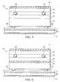
- FIG. 5is a side view of the package assembly of FIG. 3 and in accordance with a second exemplary embodiment of the present invention.
- FIG. 6is a side view of the package assembly of FIG. 3 and in accordance with a third exemplary embodiment of the present invention.
- FIGS. 3-6illustrate exemplary embodiments of the present invention.
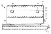
- FIG. 3depicts an integrated circuit (IC) package assembly 100 at an intermediate stage of processing.
- a semiconductor chip or die 300includes an array of internal electromagnetic structures, such as MRAM cells and access circuitry, and is shown in dotted line above a flip-chip carrier 200 .
- the flip-chip carrier 200is fabricated from a substrate 120 , an insulating layer 140 , a plurality of conductive traces (not shown) and an elastomeric layer 160 .
- the substrate 120is typically formed of a material with high mechanical stability at high temperature.
- the substrate 120may be a flexible tape such as, for example, a polyimide tape.
- Two commercially available polyimide tapes, KAPTON® from E. I. DuPont Nemours and Company and UPILEX® from Ube Industries, Ltd.,can be employed to form the substrate 120 .
- the elastomeric layer 160may be formed of a silicone or a silicone-modified epoxy.
- the conductive tracesmay be located within or on the insulating layer 140 in a variety of ways.
- One waywhich is an addition method, is to build up the conductive traces on the insulating layer 140 through electrolytic deposition.
- the electrolytic depositionmay be accomplished with a mask or, if performed without a mask, a subsequent etching step may be employed to create the conductive traces.
- Other suitable methodsinclude sputter coating and laminating a sheet of conductive material, such as copper, and etching away excess copper to form the traces.
- the conductive tracesare each electrically connected to solder balls 280 through an inset (not shown) in the substrate 120 .
- the solder balls 280are used to mount the flip-chip device carrier 200 with the chip 300 to a circuit board or other electrical structure, as it will be described in more detail below.
- the chip 300including magnetic memory structures such as MRAM cells, is shown in dotted line above the flip-chip carrier 200 .
- the chip 300is positioned on the elastomeric material 160 of the flip-chip carrier 200 , as illustrated in FIG. 4 .
- the flip-chip carrier 200is electrically connected with the chip 300 by way of suitable conductive connecting structures, such as, for example, solder balls 240 positioned within a gap 210 of the carrier 200 .
- the solder balls 240are in electrical connection with respective conductive traces 150 (not shown) and with suitable contacts on the chip 300 .
- a first magnetic shielding layer 110is provided for shielding the chip 300 from external magnetic field disturbances.
- the first magnetic shielding layer 110is formed on the back surface of the semiconductor chip 300 , that is the surface that is opposite to a front surface of the semiconductor chip 300 or the surface that directly contacts the flip-chip carrier 200 .
- the first magnetic shielding layer 110comprises a magnetic shielding material which can be formed, for example, of an electrically non-conductive material with permeability higher than that of air or silicon.
- Manganites, chromites and cobaltitesmay be used also, depending on the device characteristics and specific processing requirements.
- the magnetic shielding materialmay be also composed of conductive magnetic particles, for example nickel, iron or cobalt particles, which are incorporated into a non-conductive base material, such as a glass sealing alloy or a polyimide.
- the magnetic shielding materialmay be formed of a film or layer of conductive magnetic material, such as nickel, cobalt, iron, Permalloy, or Mumetal, among others.
- the flip-chip carrier 200 with the attached chip 300is further attached to a portion of a printed circuit board 400 by surface mounting, for example.
- the flip-chip carrier 200is mounted flat on the printed circuit board 400 and contacts the printed circuit board 400 through the solder balls 280 , eliminating the need for holes through the printed circuit board.
- a flat layer 111 of magnetic shielding materialmay be embedded within the printed circuit board, which can be otherwise formed of a resin compound, for example, or other known printed circuit board material.
- the magnetic memory structures of the chip 300are first shielded by the first magnetic shielding layer 110 and further shielded by the flat layer 111 of the printed circuit board 400 for maximum protection from external stray magnetic fields.
- FIG. 4shows the magnetic shielding material in the form of layer 110 on the backside of chip 300 and as layer 111 embedded within the printed circuit board 400
- FIG. 5illustrates another exemplary embodiment of the present invention, in which a bottom magnetic shielding layer 112 is formed on the bottom surface of the printed circuit board 400 , together with the flat layer 111 embedded within the printed circuit board 400 .
- the preferred material for the bottom magnetic shielding layer 112is a conductive Mumetal alloy comprising, for example, approximately 77% nickel (Ni), 4.8% copper (Cu), 1.5% chromium (Cr) and 14.9% iron (Fe), as well as conductive magnetic particles, such as nickel or iron particles, incorporated into a molding material, for example a glass sealing alloy or a commercially available mold compound.
- another magnetic shielding layer 113is formed of a magnetic shielding material as part of the flip-chip carrier 200 , as shown in FIG. 6 .
- the magnetic shielding layer 113is formed between the substrate 120 and the insulating layer 140 to further protect the MRAM devices from external magnetic fields and to complete the fabrication of an IC package assembly 102 (FIG. 6 ).
- the magnetic shielding materialmay be different than, or similar to, the magnetic shielding materials for layers 110 , 111 and 112 .
- Appropriate conductive vias, insulated from magnetic shielding layer 113are formed through layer 113 .
- the magnetic shielding materialmay be also composed of magnetic particles, for example nickel, iron or cobalt particles, which are incorporated into a base material such as a glass sealing alloy or a commercially available mold compound. Since nickel is conductive, however, the concentration of nickel particles in the glass alloy should be low enough so that the shielding material does not form a continuous conductor, unless appropriate conductive vias electrically insulated from the magnetic layer are used.
- the exemplary embodiments described aboverefer to specific magnetic shielding materials, it must be understood that the invention is not limited to the materials described above, and other magnetic shielding materials, such as ferromagnetics like nickel-iron (Permalloy), cobalt-nickel-iron, nickel or iron may be used also.
- ferromagneticslike nickel-iron (Permalloy), cobalt-nickel-iron, nickel or iron may be used also.
- the magnetic shielding material forming the various shielding layers described abovemay also comprise a mold compound, such as a plastic compound, with conductive magnetic particles therein.
- conductive magnetic particles of, for example, nickel, iron, and/or cobaltmay be suspended in a matrix material, such as a plastic compound, at a concentration that does not allow the particles to touch each others.
- the magnetic shielding materialmay comprise a molding material including non-conductive particles of, for example, non-conductive magnetic oxides and/or Mumetal alloys.
- Mumetal alloysmay comprise, for example, approximately 77% nickel (Ni), 4.8% copper (Cu), 1.5% chromium (Cr) and 14.9% iron (Fe).
- the exemplary embodiments described aboverefer to specific locations where the shielding material is applied to a chip, it is also possible to apply the shielding material in other locations. For example, it is also possible to apply a layer of shielding material on both the top and bottom surfaces of the printed circuit board 400 , or on the top and bottom surfaces together with a shielding material embedded within the printed circuit board. Further, a plurality of layers of material could be employed for shielding the magnetic memories structures, one on each side of chip 300 , or layers of the same or different shielding materials which overlap each other may be used on one or both sides of chip 300 , flip-chip carrier 200 and/or circuit printed board 400 .
- the specific shape of the shielding materialis not limited to that shown in FIGS. 3-6 and other shapes, configurations, or geometries may be employed.
- the chip 300 and associated flip-chip carrier 100may be encapsulated in a flip-chip package which is mountable through solder balls 180 to a printed circuit board.
Landscapes
- Physics & Mathematics (AREA)
- Engineering & Computer Science (AREA)
- Microelectronics & Electronic Packaging (AREA)
- Condensed Matter Physics & Semiconductors (AREA)
- General Physics & Mathematics (AREA)
- Computer Hardware Design (AREA)
- Power Engineering (AREA)
- Electromagnetism (AREA)
- Health & Medical Sciences (AREA)
- Toxicology (AREA)
- Mram Or Spin Memory Techniques (AREA)
- Shielding Devices Or Components To Electric Or Magnetic Fields (AREA)
Abstract
Description
Claims (12)
Priority Applications (2)
| Application Number | Priority Date | Filing Date | Title |
|---|---|---|---|
| US10/115,960US6559521B2 (en) | 2000-08-31 | 2002-04-05 | Chip carrier with magnetic shielding |
| US10/285,554US6664613B2 (en) | 2000-08-31 | 2002-11-01 | Magnetic shielding for integrated circuits |
Applications Claiming Priority (2)
| Application Number | Priority Date | Filing Date | Title |
|---|---|---|---|
| US09/653,541US6717241B1 (en) | 2000-08-31 | 2000-08-31 | Magnetic shielding for integrated circuits |
| US10/115,960US6559521B2 (en) | 2000-08-31 | 2002-04-05 | Chip carrier with magnetic shielding |
Related Parent Applications (1)
| Application Number | Title | Priority Date | Filing Date |
|---|---|---|---|
| US09/653,541DivisionUS6717241B1 (en) | 2000-08-31 | 2000-08-31 | Magnetic shielding for integrated circuits |
Related Child Applications (1)
| Application Number | Title | Priority Date | Filing Date |
|---|---|---|---|
| US10/285,554DivisionUS6664613B2 (en) | 2000-08-31 | 2002-11-01 | Magnetic shielding for integrated circuits |
Publications (2)
| Publication Number | Publication Date |
|---|---|
| US20020105058A1 US20020105058A1 (en) | 2002-08-08 |
| US6559521B2true US6559521B2 (en) | 2003-05-06 |
Family
ID=24621300
Family Applications (4)
| Application Number | Title | Priority Date | Filing Date |
|---|---|---|---|
| US09/653,541Expired - LifetimeUS6717241B1 (en) | 2000-08-31 | 2000-08-31 | Magnetic shielding for integrated circuits |
| US10/003,116Expired - LifetimeUS6924168B2 (en) | 2000-08-31 | 2001-12-06 | Method of forming a structure for supporting an integrated circuit chip |
| US10/115,960Expired - LifetimeUS6559521B2 (en) | 2000-08-31 | 2002-04-05 | Chip carrier with magnetic shielding |
| US10/285,554Expired - LifetimeUS6664613B2 (en) | 2000-08-31 | 2002-11-01 | Magnetic shielding for integrated circuits |
Family Applications Before (2)
| Application Number | Title | Priority Date | Filing Date |
|---|---|---|---|
| US09/653,541Expired - LifetimeUS6717241B1 (en) | 2000-08-31 | 2000-08-31 | Magnetic shielding for integrated circuits |
| US10/003,116Expired - LifetimeUS6924168B2 (en) | 2000-08-31 | 2001-12-06 | Method of forming a structure for supporting an integrated circuit chip |
Family Applications After (1)
| Application Number | Title | Priority Date | Filing Date |
|---|---|---|---|
| US10/285,554Expired - LifetimeUS6664613B2 (en) | 2000-08-31 | 2002-11-01 | Magnetic shielding for integrated circuits |
Country Status (1)
| Country | Link |
|---|---|
| US (4) | US6717241B1 (en) |
Cited By (23)
| Publication number | Priority date | Publication date | Assignee | Title |
|---|---|---|---|---|
| US20030098469A1 (en)* | 2000-09-25 | 2003-05-29 | Micron Technology, Inc. | Shielding arrangement to protect a circuit from stray magnetic fields |
| US20030132494A1 (en)* | 2002-01-15 | 2003-07-17 | Tuttle Mark E | Magnetic shield for integrated circuit packaging |
| US20040150091A1 (en)* | 2003-02-05 | 2004-08-05 | Stobbs Colin A. | Magnetic shielding for magnetic random access memory |
| US20050056921A1 (en)* | 2003-09-15 | 2005-03-17 | Staktek Group L.P. | Stacked module systems and methods |
| US20060263938A1 (en)* | 2005-05-18 | 2006-11-23 | Julian Partridge | Stacked module systems and method |
| US7310458B2 (en) | 2001-10-26 | 2007-12-18 | Staktek Group L.P. | Stacked module systems and methods |
| US20080036070A1 (en)* | 2003-12-02 | 2008-02-14 | Great Wall Semiconductor Corporation | Bond Wireless Package |
| US7335975B2 (en) | 2001-10-26 | 2008-02-26 | Staktek Group L.P. | Integrated circuit stacking system and method |
| US7371609B2 (en) | 2001-10-26 | 2008-05-13 | Staktek Group L.P. | Stacked module systems and methods |
| US20080122047A1 (en)* | 2006-10-13 | 2008-05-29 | Tessera, Inc. | Collective and synergistic MRAM shields |
| US20080122054A1 (en)* | 2006-11-02 | 2008-05-29 | Leland Szewerenko | Circuit Module Having Force Resistant Construction |
| US20080296690A1 (en)* | 2003-12-12 | 2008-12-04 | Great Wall Semiconductor Corporation | Metal interconnect System and Method for Direct Die Attachment |
| US7485951B2 (en) | 2001-10-26 | 2009-02-03 | Entorian Technologies, Lp | Modularized die stacking system and method |
| US20090045488A1 (en)* | 2007-08-13 | 2009-02-19 | Industrial Technology Research Institute | Magnetic shielding package structure of a magnetic memory device |
| US7495334B2 (en) | 2001-10-26 | 2009-02-24 | Entorian Technologies, Lp | Stacking system and method |
| US7524703B2 (en) | 2001-10-26 | 2009-04-28 | Entorian Technologies, Lp | Integrated circuit stacking system and method |
| US7542304B2 (en) | 2003-09-15 | 2009-06-02 | Entorian Technologies, Lp | Memory expansion and integrated circuit stacking system and method |
| US7626273B2 (en) | 2001-10-26 | 2009-12-01 | Entorian Technologies, L.P. | Low profile stacking system and method |
| US7656678B2 (en) | 2001-10-26 | 2010-02-02 | Entorian Technologies, Lp | Stacked module systems |
| US7719098B2 (en) | 2001-10-26 | 2010-05-18 | Entorian Technologies Lp | Stacked modules and method |
| US8415775B2 (en) | 2010-11-23 | 2013-04-09 | Honeywell International Inc. | Magnetic shielding for multi-chip module packaging |
| US10347826B1 (en) | 2018-01-08 | 2019-07-09 | Globalfoundries Singapore Pte. Ltd. | STT-MRAM flip-chip magnetic shielding and method for producing the same |
| US10361162B1 (en) | 2018-01-23 | 2019-07-23 | Globalfoundries Singapore Pte. Ltd. | Magnetic shielding of STT-MRAM in multichip packaging and method of manufacturing the same |
Families Citing this family (36)
| Publication number | Priority date | Publication date | Assignee | Title |
|---|---|---|---|---|
| US7940716B2 (en) | 2005-07-01 | 2011-05-10 | Terahop Networks, Inc. | Maintaining information facilitating deterministic network routing |
| US7733818B2 (en)* | 2000-12-22 | 2010-06-08 | Terahop Networks, Inc. | Intelligent node communication using network formation messages in a mobile Ad hoc network |
| US7830850B2 (en)* | 2000-12-22 | 2010-11-09 | Terahop Networks, Inc. | Class-switching in class-based data communcations network |
| US7574168B2 (en)* | 2005-06-16 | 2009-08-11 | Terahop Networks, Inc. | Selective GPS denial system |
| US7522568B2 (en)* | 2000-12-22 | 2009-04-21 | Terahop Networks, Inc. | Propagating ad hoc wireless networks based on common designation and routine |
| US8050625B2 (en)* | 2000-12-22 | 2011-11-01 | Terahop Networks, Inc. | Wireless reader tags (WRTs) with sensor components in asset monitoring and tracking systems |
| US7583769B2 (en)* | 2005-06-16 | 2009-09-01 | Terahop Netowrks, Inc. | Operating GPS receivers in GPS-adverse environment |
| US7783246B2 (en)* | 2005-06-16 | 2010-08-24 | Terahop Networks, Inc. | Tactical GPS denial and denial detection system |
| JP2002353369A (en)* | 2001-05-28 | 2002-12-06 | Sharp Corp | Semiconductor package and manufacturing method thereof |
| US7176055B2 (en)* | 2001-11-02 | 2007-02-13 | Matsushita Electric Industrial Co., Ltd. | Method and apparatus for manufacturing electronic component-mounted component, and electronic component-mounted component |
| US6724027B2 (en)* | 2002-04-18 | 2004-04-20 | Hewlett-Packard Development Company, L.P. | Magnetic shielding for MRAM devices |
| DE10229542B4 (en) | 2002-07-01 | 2004-05-19 | Infineon Technologies Ag | Electronic component with multilayer rewiring plate and method for producing the same |
| JP2004047656A (en)* | 2002-07-11 | 2004-02-12 | Sony Corp | Magnetic nonvolatile memory device and method of manufacturing the same |
| US7037604B2 (en)* | 2002-07-23 | 2006-05-02 | Honeywell International, Inc. | Magnetic sensing device |
| JP4096302B2 (en)* | 2002-12-16 | 2008-06-04 | ソニー株式会社 | Magnetic memory device |
| US6838721B2 (en)* | 2003-04-25 | 2005-01-04 | Freescale Semiconductor, Inc. | Integrated circuit with a transitor over an interconnect layer |
| JP4742502B2 (en)* | 2004-02-23 | 2011-08-10 | ソニー株式会社 | Magnetic shield body, magnetic shield structure, and magnetic memory device |
| CN100514604C (en) | 2004-03-12 | 2009-07-15 | 株式会社半导体能源研究所 | Semiconductor device with a plurality of transistors |
| US7142107B2 (en) | 2004-05-27 | 2006-11-28 | Lawrence Kates | Wireless sensor unit |
| US7799428B2 (en)* | 2004-10-06 | 2010-09-21 | Graftech International Holdings Inc. | Sandwiched thermal solution |
| US7183617B2 (en)* | 2005-02-17 | 2007-02-27 | Taiwan Semiconductor Manufacturing Co., Ltd. | Magnetic shielding for magnetically sensitive semiconductor devices |
| US7445942B2 (en)* | 2005-07-15 | 2008-11-04 | Magic Technologies, Inc. | Process for manufacturing segmented MRAM array with patterned segmented magnetic shields |
| WO2007067831A1 (en)* | 2005-10-31 | 2007-06-14 | Terahop Networks, Inc. | Determining relative elevation using gps and ranging |
| US20090129306A1 (en) | 2007-02-21 | 2009-05-21 | Terahop Networks, Inc. | Wake-up broadcast including network information in common designation ad hoc wireless networking |
| US7795708B2 (en)* | 2006-06-02 | 2010-09-14 | Honeywell International Inc. | Multilayer structures for magnetic shielding |
| US7985621B2 (en)* | 2006-08-31 | 2011-07-26 | Ati Technologies Ulc | Method and apparatus for making semiconductor packages |
| US8223680B2 (en)* | 2007-02-21 | 2012-07-17 | Google Inc. | Mesh network control using common designation wake-up |
| WO2009151877A2 (en) | 2008-05-16 | 2009-12-17 | Terahop Networks, Inc. | Systems and apparatus for securing a container |
| US8391435B2 (en) | 2008-12-25 | 2013-03-05 | Google Inc. | Receiver state estimation in a duty cycled radio |
| CN101958597B (en)* | 2009-07-15 | 2013-11-06 | 鸿富锦精密工业(深圳)有限公司 | Electromagnetic shielding material, electromagnetic shielding shell and voice coil motor |
| JP5729186B2 (en)* | 2011-07-14 | 2015-06-03 | 富士通セミコンダクター株式会社 | Semiconductor device and manufacturing method thereof |
| WO2015047324A1 (en) | 2013-09-27 | 2015-04-02 | Intel Corporation | Magnetic field shielding for packaging build-up architectures |
| KR102214798B1 (en) | 2014-02-05 | 2021-02-10 | 삼성전자주식회사 | Package substrate and semiconductor package including the same |
| CN107534018B (en)* | 2015-04-27 | 2020-06-16 | 东芝存储器株式会社 | magnetic memory device |
| US10559536B2 (en)* | 2018-06-26 | 2020-02-11 | Abb Schweiz Ag | Multi-layer conductors for noise reduction in power electronics |
| CN115411175A (en)* | 2021-05-26 | 2022-11-29 | 浙江驰拓科技有限公司 | A kind of magnetic assembly and packaging method thereof |
Citations (6)
| Publication number | Priority date | Publication date | Assignee | Title |
|---|---|---|---|---|
| US4656499A (en) | 1982-08-05 | 1987-04-07 | Olin Corporation | Hermetically sealed semiconductor casing |
| US5288238A (en) | 1991-04-30 | 1994-02-22 | Itt Industries, Inc. | IC chip to PC board connector system |
| US5352925A (en)* | 1991-03-27 | 1994-10-04 | Kokusai Electric Co., Ltd. | Semiconductor device with electromagnetic shield |
| US5371404A (en)* | 1993-02-04 | 1994-12-06 | Motorola, Inc. | Thermally conductive integrated circuit package with radio frequency shielding |
| US5490786A (en) | 1994-03-25 | 1996-02-13 | Itt Corporation | Termination of contact tails to PC board |
| US5939772A (en) | 1997-10-31 | 1999-08-17 | Honeywell Inc. | Shielded package for magnetic devices |
Family Cites Families (27)
| Publication number | Priority date | Publication date | Assignee | Title |
|---|---|---|---|---|
| US3743978A (en)* | 1969-12-09 | 1973-07-03 | W Fritz | Coated ferrite rf filters |
| US4408255A (en)* | 1981-01-12 | 1983-10-04 | Harold Adkins | Absorptive electromagnetic shielding for high speed computer applications |
| US4433886A (en)* | 1981-12-17 | 1984-02-28 | Elco Corporation | Connector mounting for integrated circuit chip packages |
| US4835598A (en)* | 1985-06-13 | 1989-05-30 | Matsushita Electric Works, Ltd. | Wiring board |
| CA1261481A (en)* | 1986-03-13 | 1989-09-26 | Kazumasa Eguchi | Printed circuit board capable of preventing electromagnetic interference |
| US4953002A (en) | 1988-03-31 | 1990-08-28 | Honeywell Inc. | Semiconductor device housing with magnetic field protection |
| JP2536819Y2 (en)* | 1990-09-17 | 1997-05-28 | 富士写真フイルム株式会社 | Magnetic head device for camera |
| US5357404A (en)* | 1991-11-18 | 1994-10-18 | The Whitaker Corporation | EMI shield, and assembly using same |
| KR100260347B1 (en)* | 1992-06-05 | 2000-07-01 | 나까니시 히로유끼 | 3D printed board, electronic circuit package and printed board manufacturing method using the same |
| US5418688A (en)* | 1993-03-29 | 1995-05-23 | Motorola, Inc. | Cardlike electronic device |
| US5406117A (en)* | 1993-12-09 | 1995-04-11 | Dlugokecki; Joseph J. | Radiation shielding for integrated circuit devices using reconstructed plastic packages |
| US5639989A (en)* | 1994-04-19 | 1997-06-17 | Motorola Inc. | Shielded electronic component assembly and method for making the same |
| US5436203A (en)* | 1994-07-05 | 1995-07-25 | Motorola, Inc. | Shielded liquid encapsulated semiconductor device and method for making the same |
| US5811317A (en)* | 1995-08-25 | 1998-09-22 | Texas Instruments Incorporated | Process for reflow bonding a semiconductor die to a substrate and the product produced by the product |
| US5789142A (en)* | 1996-01-16 | 1998-08-04 | Motorola, Inc. | Solder mask system |
| US5689878A (en)* | 1996-04-17 | 1997-11-25 | Lucent Technologies Inc. | Method for protecting electronic circuit components |
| US5864092A (en)* | 1996-05-16 | 1999-01-26 | Sawtek Inc. | Leadless ceramic chip carrier crosstalk suppression apparatus |
| US5949654A (en)* | 1996-07-03 | 1999-09-07 | Kabushiki Kaisha Toshiba | Multi-chip module, an electronic device, and production method thereof |
| US5783857A (en)* | 1996-07-25 | 1998-07-21 | The Whitaker Corporation | Integrated circuit package |
| US5902690A (en) | 1997-02-25 | 1999-05-11 | Motorola, Inc. | Stray magnetic shielding for a non-volatile MRAM |
| US5866943A (en)* | 1997-06-23 | 1999-02-02 | Lsi Logic Corporation | System and method for forming a grid array device package employing electomagnetic shielding |
| US6109530A (en)* | 1998-07-08 | 2000-08-29 | Motorola, Inc. | Integrated circuit carrier package with battery coin cell |
| US5977626A (en)* | 1998-08-12 | 1999-11-02 | Industrial Technology Research Institute | Thermally and electrically enhanced PBGA package |
| US6191360B1 (en)* | 1999-04-26 | 2001-02-20 | Advanced Semiconductor Engineering, Inc. | Thermally enhanced BGA package |
| US6104610A (en)* | 1999-07-29 | 2000-08-15 | Tilton; Charles L. | EMI shielding fluid control apparatus |
| US6288344B1 (en)* | 1999-08-20 | 2001-09-11 | Cardiac Pacemakers, Inc. | Integrated EMI shield utilizing a hybrid edge |
| US6229207B1 (en)* | 2000-01-13 | 2001-05-08 | Advanced Micro Devices, Inc. | Organic pin grid array flip chip carrier package |
- 2000
- 2000-08-31USUS09/653,541patent/US6717241B1/ennot_activeExpired - Lifetime
- 2001
- 2001-12-06USUS10/003,116patent/US6924168B2/ennot_activeExpired - Lifetime
- 2002
- 2002-04-05USUS10/115,960patent/US6559521B2/ennot_activeExpired - Lifetime
- 2002-11-01USUS10/285,554patent/US6664613B2/ennot_activeExpired - Lifetime
Patent Citations (6)
| Publication number | Priority date | Publication date | Assignee | Title |
|---|---|---|---|---|
| US4656499A (en) | 1982-08-05 | 1987-04-07 | Olin Corporation | Hermetically sealed semiconductor casing |
| US5352925A (en)* | 1991-03-27 | 1994-10-04 | Kokusai Electric Co., Ltd. | Semiconductor device with electromagnetic shield |
| US5288238A (en) | 1991-04-30 | 1994-02-22 | Itt Industries, Inc. | IC chip to PC board connector system |
| US5371404A (en)* | 1993-02-04 | 1994-12-06 | Motorola, Inc. | Thermally conductive integrated circuit package with radio frequency shielding |
| US5490786A (en) | 1994-03-25 | 1996-02-13 | Itt Corporation | Termination of contact tails to PC board |
| US5939772A (en) | 1997-10-31 | 1999-08-17 | Honeywell Inc. | Shielded package for magnetic devices |
Cited By (41)
| Publication number | Priority date | Publication date | Assignee | Title |
|---|---|---|---|---|
| US6916668B2 (en) | 2000-09-25 | 2005-07-12 | Micron Technology, Inc. | Methods for providing a magnetic shield for an integrated circuit having magnetoresistive memory cells |
| US20030098469A1 (en)* | 2000-09-25 | 2003-05-29 | Micron Technology, Inc. | Shielding arrangement to protect a circuit from stray magnetic fields |
| US7569915B2 (en) | 2000-09-25 | 2009-08-04 | Micron Technology, Inc. | Shielding arrangement to protect a circuit from stray magnetic fields |
| US20060237823A1 (en)* | 2000-09-25 | 2006-10-26 | Micron Technology, Inc. | Shielding arrangement to protect a circuit from stray magnetic fields |
| US7078243B2 (en) | 2000-09-25 | 2006-07-18 | Micron Technology, Inc. | Shielding arrangement to protect a circuit from stray magnetic fields |
| US20050130327A1 (en)* | 2000-09-25 | 2005-06-16 | Micron Technology, Inc. | Shielding arrangement to protect a circuit from stray magnetic fields |
| US7595550B2 (en) | 2001-10-26 | 2009-09-29 | Entorian Technologies, Lp | Flex-based circuit module |
| US7626273B2 (en) | 2001-10-26 | 2009-12-01 | Entorian Technologies, L.P. | Low profile stacking system and method |
| US7719098B2 (en) | 2001-10-26 | 2010-05-18 | Entorian Technologies Lp | Stacked modules and method |
| US7656678B2 (en) | 2001-10-26 | 2010-02-02 | Entorian Technologies, Lp | Stacked module systems |
| US7586758B2 (en) | 2001-10-26 | 2009-09-08 | Entorian Technologies, Lp | Integrated circuit stacking system |
| US7572671B2 (en) | 2001-10-26 | 2009-08-11 | Entorian Technologies, Lp | Stacked module systems and methods |
| US7310458B2 (en) | 2001-10-26 | 2007-12-18 | Staktek Group L.P. | Stacked module systems and methods |
| US7524703B2 (en) | 2001-10-26 | 2009-04-28 | Entorian Technologies, Lp | Integrated circuit stacking system and method |
| US7495334B2 (en) | 2001-10-26 | 2009-02-24 | Entorian Technologies, Lp | Stacking system and method |
| US7335975B2 (en) | 2001-10-26 | 2008-02-26 | Staktek Group L.P. | Integrated circuit stacking system and method |
| US7371609B2 (en) | 2001-10-26 | 2008-05-13 | Staktek Group L.P. | Stacked module systems and methods |
| US7485951B2 (en) | 2001-10-26 | 2009-02-03 | Entorian Technologies, Lp | Modularized die stacking system and method |
| US20060019422A1 (en)* | 2002-01-15 | 2006-01-26 | Tuttle Mark E | Magnetic shield for integrated circuit packaging |
| US6962833B2 (en) | 2002-01-15 | 2005-11-08 | Micron Technology, Inc. | Magnetic shield for integrated circuit packaging |
| US20030132494A1 (en)* | 2002-01-15 | 2003-07-17 | Tuttle Mark E | Magnetic shield for integrated circuit packaging |
| US20040119095A1 (en)* | 2002-01-15 | 2004-06-24 | Tuttle Mark E | Magnetic shield for integrated circuit packaging |
| US20040150091A1 (en)* | 2003-02-05 | 2004-08-05 | Stobbs Colin A. | Magnetic shielding for magnetic random access memory |
| US7489015B2 (en) | 2003-02-05 | 2009-02-10 | Samsung Electronics Co., Ltd. | Magnetic shielding for magnetic random access memory |
| US20050056921A1 (en)* | 2003-09-15 | 2005-03-17 | Staktek Group L.P. | Stacked module systems and methods |
| US7542304B2 (en) | 2003-09-15 | 2009-06-02 | Entorian Technologies, Lp | Memory expansion and integrated circuit stacking system and method |
| US20080036070A1 (en)* | 2003-12-02 | 2008-02-14 | Great Wall Semiconductor Corporation | Bond Wireless Package |
| US20080296690A1 (en)* | 2003-12-12 | 2008-12-04 | Great Wall Semiconductor Corporation | Metal interconnect System and Method for Direct Die Attachment |
| US20060263938A1 (en)* | 2005-05-18 | 2006-11-23 | Julian Partridge | Stacked module systems and method |
| US7323364B2 (en) | 2005-05-18 | 2008-01-29 | Staktek Group L.P. | Stacked module systems and method |
| US20080122047A1 (en)* | 2006-10-13 | 2008-05-29 | Tessera, Inc. | Collective and synergistic MRAM shields |
| US8269319B2 (en)* | 2006-10-13 | 2012-09-18 | Tessera, Inc. | Collective and synergistic MRAM shields |
| US20080122054A1 (en)* | 2006-11-02 | 2008-05-29 | Leland Szewerenko | Circuit Module Having Force Resistant Construction |
| US7417310B2 (en) | 2006-11-02 | 2008-08-26 | Entorian Technologies, Lp | Circuit module having force resistant construction |
| US7804985B2 (en) | 2006-11-02 | 2010-09-28 | Entorian Technologies Lp | Circuit module having force resistant construction |
| US20090045488A1 (en)* | 2007-08-13 | 2009-02-19 | Industrial Technology Research Institute | Magnetic shielding package structure of a magnetic memory device |
| US7772679B2 (en) | 2007-08-13 | 2010-08-10 | Industrial Technology Research Institute | Magnetic shielding package structure of a magnetic memory device |
| US8415775B2 (en) | 2010-11-23 | 2013-04-09 | Honeywell International Inc. | Magnetic shielding for multi-chip module packaging |
| US10347826B1 (en) | 2018-01-08 | 2019-07-09 | Globalfoundries Singapore Pte. Ltd. | STT-MRAM flip-chip magnetic shielding and method for producing the same |
| US10361162B1 (en) | 2018-01-23 | 2019-07-23 | Globalfoundries Singapore Pte. Ltd. | Magnetic shielding of STT-MRAM in multichip packaging and method of manufacturing the same |
| US11018093B2 (en) | 2018-01-23 | 2021-05-25 | Globalfoundries Singapore Pte. Ltd. | Magnetic shielding of STT-MRAM in multichip packaging and method of manufacturing the same |
Also Published As
| Publication number | Publication date |
|---|---|
| US6717241B1 (en) | 2004-04-06 |
| US6924168B2 (en) | 2005-08-02 |
| US6664613B2 (en) | 2003-12-16 |
| US20020105058A1 (en) | 2002-08-08 |
| US20030052340A1 (en) | 2003-03-20 |
| US20020050632A1 (en) | 2002-05-02 |
Similar Documents
| Publication | Publication Date | Title |
|---|---|---|
| US6559521B2 (en) | Chip carrier with magnetic shielding | |
| US6452253B1 (en) | Method and apparatus for magnetic shielding of an integrated circuit | |
| US7489015B2 (en) | Magnetic shielding for magnetic random access memory | |
| US8269319B2 (en) | Collective and synergistic MRAM shields | |
| US6962833B2 (en) | Magnetic shield for integrated circuit packaging | |
| US6625040B1 (en) | Shielded PC board for magnetically sensitive integrated circuits | |
| US9070692B2 (en) | Shields for magnetic memory chip packages | |
| US7829980B2 (en) | Magnetoresistive device and method of packaging same | |
| US7294910B2 (en) | Electronic component with multilayered rewiring plate and method for producing the same | |
| US6984867B2 (en) | Magnetic memory device | |
| JP2003115578A (en) | Non-volatile solid-state magnetic memory device, method of manufacturing the same, and multi-chip package | |
| KR102378232B1 (en) | Devices and methods having magnetic shielding layer | |
| US6967390B2 (en) | Electronic component and method of manufacturing same | |
| WO2011111789A1 (en) | Magnetic device and process for production thereof | |
| KR102624903B1 (en) | MRAM Package with Magnetic Shielding Layer and Method of Manufacturing the Same |
Legal Events
| Date | Code | Title | Description |
|---|---|---|---|
| STCF | Information on status: patent grant | Free format text:PATENTED CASE | |
| FPAY | Fee payment | Year of fee payment:4 | |
| FPAY | Fee payment | Year of fee payment:8 | |
| FEPP | Fee payment procedure | Free format text:PAYOR NUMBER ASSIGNED (ORIGINAL EVENT CODE: ASPN); ENTITY STATUS OF PATENT OWNER: LARGE ENTITY | |
| FPAY | Fee payment | Year of fee payment:12 | |
| AS | Assignment | Owner name:U.S. BANK NATIONAL ASSOCIATION, AS COLLATERAL AGENT, CALIFORNIA Free format text:SECURITY INTEREST;ASSIGNOR:MICRON TECHNOLOGY, INC.;REEL/FRAME:038669/0001 Effective date:20160426 Owner name:U.S. BANK NATIONAL ASSOCIATION, AS COLLATERAL AGEN Free format text:SECURITY INTEREST;ASSIGNOR:MICRON TECHNOLOGY, INC.;REEL/FRAME:038669/0001 Effective date:20160426 | |
| AS | Assignment | Owner name:MORGAN STANLEY SENIOR FUNDING, INC., AS COLLATERAL AGENT, MARYLAND Free format text:PATENT SECURITY AGREEMENT;ASSIGNOR:MICRON TECHNOLOGY, INC.;REEL/FRAME:038954/0001 Effective date:20160426 Owner name:MORGAN STANLEY SENIOR FUNDING, INC., AS COLLATERAL Free format text:PATENT SECURITY AGREEMENT;ASSIGNOR:MICRON TECHNOLOGY, INC.;REEL/FRAME:038954/0001 Effective date:20160426 | |
| AS | Assignment | Owner name:U.S. BANK NATIONAL ASSOCIATION, AS COLLATERAL AGENT, CALIFORNIA Free format text:CORRECTIVE ASSIGNMENT TO CORRECT THE REPLACE ERRONEOUSLY FILED PATENT #7358718 WITH THE CORRECT PATENT #7358178 PREVIOUSLY RECORDED ON REEL 038669 FRAME 0001. ASSIGNOR(S) HEREBY CONFIRMS THE SECURITY INTEREST;ASSIGNOR:MICRON TECHNOLOGY, INC.;REEL/FRAME:043079/0001 Effective date:20160426 Owner name:U.S. BANK NATIONAL ASSOCIATION, AS COLLATERAL AGEN Free format text:CORRECTIVE ASSIGNMENT TO CORRECT THE REPLACE ERRONEOUSLY FILED PATENT #7358718 WITH THE CORRECT PATENT #7358178 PREVIOUSLY RECORDED ON REEL 038669 FRAME 0001. ASSIGNOR(S) HEREBY CONFIRMS THE SECURITY INTEREST;ASSIGNOR:MICRON TECHNOLOGY, INC.;REEL/FRAME:043079/0001 Effective date:20160426 | |
| AS | Assignment | Owner name:JPMORGAN CHASE BANK, N.A., AS COLLATERAL AGENT, ILLINOIS Free format text:SECURITY INTEREST;ASSIGNORS:MICRON TECHNOLOGY, INC.;MICRON SEMICONDUCTOR PRODUCTS, INC.;REEL/FRAME:047540/0001 Effective date:20180703 Owner name:JPMORGAN CHASE BANK, N.A., AS COLLATERAL AGENT, IL Free format text:SECURITY INTEREST;ASSIGNORS:MICRON TECHNOLOGY, INC.;MICRON SEMICONDUCTOR PRODUCTS, INC.;REEL/FRAME:047540/0001 Effective date:20180703 | |
| AS | Assignment | Owner name:MICRON TECHNOLOGY, INC., IDAHO Free format text:RELEASE BY SECURED PARTY;ASSIGNOR:U.S. BANK NATIONAL ASSOCIATION, AS COLLATERAL AGENT;REEL/FRAME:047243/0001 Effective date:20180629 | |
| AS | Assignment | Owner name:MICRON TECHNOLOGY, INC., IDAHO Free format text:RELEASE BY SECURED PARTY;ASSIGNOR:MORGAN STANLEY SENIOR FUNDING, INC., AS COLLATERAL AGENT;REEL/FRAME:050937/0001 Effective date:20190731 | |
| AS | Assignment | Owner name:MICRON TECHNOLOGY, INC., IDAHO Free format text:RELEASE BY SECURED PARTY;ASSIGNOR:JPMORGAN CHASE BANK, N.A., AS COLLATERAL AGENT;REEL/FRAME:051028/0001 Effective date:20190731 Owner name:MICRON SEMICONDUCTOR PRODUCTS, INC., IDAHO Free format text:RELEASE BY SECURED PARTY;ASSIGNOR:JPMORGAN CHASE BANK, N.A., AS COLLATERAL AGENT;REEL/FRAME:051028/0001 Effective date:20190731 |