US6559048B1 - Method of making a sloped sidewall via for integrated circuit structure to suppress via poisoning - Google Patents
Method of making a sloped sidewall via for integrated circuit structure to suppress via poisoningDownload PDFInfo
- Publication number
- US6559048B1 US6559048B1US09/870,851US87085101AUS6559048B1US 6559048 B1US6559048 B1US 6559048B1US 87085101 AUS87085101 AUS 87085101AUS 6559048 B1US6559048 B1US 6559048B1
- Authority
- US
- United States
- Prior art keywords
- dielectric material
- resist mask
- layer
- low
- vias
- Prior art date
- Legal status (The legal status is an assumption and is not a legal conclusion. Google has not performed a legal analysis and makes no representation as to the accuracy of the status listed.)
- Expired - Lifetime
Links
Images


Classifications
- H—ELECTRICITY
- H01—ELECTRIC ELEMENTS
- H01L—SEMICONDUCTOR DEVICES NOT COVERED BY CLASS H10
- H01L21/00—Processes or apparatus adapted for the manufacture or treatment of semiconductor or solid state devices or of parts thereof
- H01L21/70—Manufacture or treatment of devices consisting of a plurality of solid state components formed in or on a common substrate or of parts thereof; Manufacture of integrated circuit devices or of parts thereof
- H01L21/71—Manufacture of specific parts of devices defined in group H01L21/70
- H01L21/768—Applying interconnections to be used for carrying current between separate components within a device comprising conductors and dielectrics
- H01L21/76801—Applying interconnections to be used for carrying current between separate components within a device comprising conductors and dielectrics characterised by the formation and the after-treatment of the dielectrics, e.g. smoothing
- H01L21/76802—Applying interconnections to be used for carrying current between separate components within a device comprising conductors and dielectrics characterised by the formation and the after-treatment of the dielectrics, e.g. smoothing by forming openings in dielectrics
- H01L21/76804—Applying interconnections to be used for carrying current between separate components within a device comprising conductors and dielectrics characterised by the formation and the after-treatment of the dielectrics, e.g. smoothing by forming openings in dielectrics by forming tapered via holes
Definitions
- This inventionrelates to integrated circuit structures. More particularly this invention relates to improvements in the plasma etching of low dielectric constant (low k) carbon-containing silicon oxide dielectric material used in the formation of integrated circuit structures.
- low dielectric constant (low k) carbon-containing silicon oxide dielectric materialused in the formation of integrated circuit structures.
- the processis said to react methyl silane (CH 3 —SiH 3 ) with hydrogen peroxide (H 2 O 2 ) to form monosilicic acid which condenses on a cool wafer and is converted into an amorphous methyl-doped silicon oxide which is annealed at 400° C. to remove moisture.
- methyl silaneCH 3 —SiH 3
- hydrogen peroxideH 2 O 2
- carbon-doped silicon oxide dielectric materialinto interconnect architecture has been very attractive not only because of the low k properties, but also because of the compatibility with conventional silicon process technologies. Generally these materials remain stable upon annealing at temperatures of up to 500° C.
- the carbon doped silicon oxide materialsare characterized by the structure of amorphous silicon oxide with incorporated methyl groups and hydrogen species, and are also characterized by a reduced density in comparison with conventional silicon oxide that can be explained by the formation of microporosity surrounding the incorporated methyl groups.
- hydrocarbon-modified silicon oxide dielectric materials deposited by CVD techniquesare also characterized by strong adhesion.
- While such carbon-doped silicon oxide dielectric materialsdo exhibit the desired low k (i.e., dielectric constants below about 3.0), resulting in reduced capacitance of the dielectric material, a major problem of such carbon-doped silicon oxide is a low resistance to oxidation that results in a destruction of the incorporated hydrocarbons and a resulting increase in the overall dielectric constant of the dielectric material.
- the sensitivity to oxidationis thought to be due to the reactivity of the C—H bonds of the methyl group bonded to silicon.
- the removal of the methyl groupresults in a more hydrophilic surface that may be responsible for a so-called “via poisoning” which is observed after via etch and photoresist strip with oxygen-containing plasma, and is believed to be related to suppression of the surface nucleation in subsequent via liner deposition steps, resulting in incomplete or inadequate filling of the via with metal filler.
- FIG. 1 and 2illustrate a typical prior art formation of vias in low k dielectric material.
- a layer 10 of 10 ′′′ k dielectric materialhas been previously formed over a dielectric structure 2 .
- a conventional photoresist mask 14is shown formed over low k dielectric layer 10 with a straight sidewall via mask opening 16 formed therein.
- FIG. 2shows the structure of FIG. 1 after etching of a via opening 12 in low k dielectric layer 10 .
- via poisoningmay be due to damage to the low k dielectric material comprising the sidewalls of the via, resulting in the absorption of moisture into the low k dielectric material which is then released by the damaged low k dielectric material during subsequent processing, including the via filling step. Alternately, or in addition, such via poisoning may be the result of the presence of etch residues remaining in the via as a result of inadequate cleaning of the via after either formation of the via or removal of the resist mask or both.
- via poisoning of vias formed in low k carbon-containing silicon oxide dielectric materialis suppressed by forming the via in a layer of such dielectric material with a smooth inwardly sloped sidewall.
- a sloped sidewall viacan be etched in a low k dielectric layer by first forming a via resist mask over the upper surface of such a dielectric layer, then heat treating the mask sufficiently to deform the sidewall geometry of the resist mask to form a sloped or rounded sidewall on the opening or openings in the heat treated resist mask.
- the smoothness of the sloped sidewall of the resulting viais enhanced by adjusting the selectivity of the via etch to uniformly etch each of the layers of dielectric material at approximately the same rate.
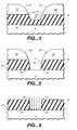
- FIG. 1is a fragmentary vertical side-section view of a prior art integrated circuit structure with a conventional prior art photoresist mask having straight sidewalls shown formed over a low k dielectric layer before etching of a via in the low k dielectric layer through the opening in the photoresist mask.
- FIG. 2is a fragmentary vertical side-section view of the prior art structure of FIG. 1 with a straight-sidewall via shown etched in the low k dielectric layer through the straight-sidewall opening in the prior art photoresist mask.
- FIG. 3is a fragmentary vertical side-section view of the prior art structure of FIG. 1 after heat treatment of the photoresist mask in accordance with the invention to form a resist mask with sloped sidewall openings.
- FIG. 4is a fragmentary vertical side-section view of the structure of FIG. 3 after partial etching of a tapered via in the low k dielectric material through the heat treated resist mask with sloped sidewall openings.
- FIG. 5is a fragmentary vertical side-section view of the structure of FIG. 3 after completion of the etching of a tapered via in the low k dielectric material through the heat treated resist mask with sloped sidewall openings.
- FIG. 6is a fragmentary vertical side-section view of the structure of FIG. 5 after removal of the heat treated resist mask with sloped sidewall openings, with the sloped or tapered sidewall via ready for filling with one or more metals and/or one or more electrically conductive metal compounds.
- FIG. 7is a top-down scanning electron microscope (SEM) view of the slanted sidewall via showing, in white, the difference in diameter between the small bottom opening of the slanted sidewall via and the large opening of the slanted sidewall via at the top.
- SEMscanning electron microscope
- FIG. 8is a fragmentary vertical side-section view of a prior art integrated circuit structure with multiple layers of different dielectric materials wherein at least one of the multiple layers of dielectric materials is a layer of low k dielectric material, showing a via cut through the multiple layers of different dielectric materials and illustrating, in exaggerated form, the resulting uneven via sidewall edges when the various layers of different dielectric materials do not etch at the same rate.
- FIG. 9is a fragmentary vertical side-section view of an integrated circuit structure with multiple layers of different dielectric materials showing the formation of a smoothly tapered or sloped sidewall via formed therein in accordance with the invention, using a heat treated photoresist mask with sloped sidewall openings and an etch system which uniformly etches all of the layers of different dielectric materials.
- via poisoning of vias formed in low k carbon-containing silicon oxide dielectric materialis suppressed by forming the via in a layer of such dielectric material with a smooth inwardly sloped sidewall.
- a sloped sidewall viacan be etched in a low k dielectric layer by first forming a via resist mask over the upper surface of such a dielectric layer, then heat treating the mask sufficiently to deform the sidewall geometry of the resist mask to form a sloped sidewall on the opening or openings in the heat treated resist mask.
- inwardly sloped sidewallwith respect to the description of the via formed in the dielectric layer beneath the heat treated resist mask, is meant a via sidewall surface which is sloped to provide a larger diameter in the via adjacent the resist mask and a smaller via diameter at the bottom or opposite end of the via.
- low k dielectric materiala dielectric material having a dielectric constant below about 4, preferably below about 3.5, and most preferably below 3.0.
- dielectric materialmay comprise, by way of example, a carbon-containing silicon oxide formed by the reaction of a carbon-containing source of silicon with an oxidizing agent.
- Examples of such carbon-containing sources of siliconinclude the methyl-containing silanes described in the previously discussed Peters and McClatchie et al. articles and the carbon-containing silicon precursors described in U.S. Pat. No. 6,303,047, issued Oct. 16, 2001, assigned to the assignee of this invention, and the subject matter of which is hereby incorporated by reference.
- the desired sloped sidewall via of the inventionis made by first forming, over the upper surface of the layer of low k dielectric material in which the desired sloped sidewall via is to be formed, a via resist mask having one or more openings therein.
- the resist maskneed not be formed directly over the layer of low k dielectric material.
- the layer of low k dielectric materialwill be formed with a thin (e.g., 300-1000 Angstroms) protective capping layer of conventional dielectric constant dielectric material formed over the layer of low k dielectric material to protect the otherwise exposed upper surface of the low k dielectric layer.
- the resist maskat this point, will resemble the prior art resist mask 14 with straight sidewalls.
- the resist maskis then heat treated sufficiently to deform the sidewall geometry of the resist mask to form a sloped sidewall on each of the one or more openings in the resist mask. This is shown in FIG. 3 where a heat treated resist mask 20 is shown with an opening 26 therein having sloped sidewalls 30 .
- Heat treated resist mask 20is formed by heat treating a photolithographically processed organic photoresist mask layer on a dielectric layer at a minimum time and temperature sufficient to cause enough flow of the resist material to cause the upper corner of the openings already formed therein to be sloped. Temperatures higher that such a minimum temperature may be used, provided however, that the heat treatment temperature must be maintained below a temperature which would burn and/or destroy the resist material or destroy the integrity of the resist material as a mask.
- the resist maskis heat treated at a temperature ranging from about 100° C. to about 300° C., and most preferably at a temperature ranging from about 150° C. to about 250° C., with the heat treatment typically carried out at a temperature of about 170° C.
- the heat treatment of the resist maskis preferably carried out for a time period ranging from about 30 second to about 5 minutes, and typically for about 2 minutes.
- etching of the underling layer of dielectric materialis commenced, using an etchant system selective to the material, such as another metal layer, lying below the dielectric layer to be etched.
- the etchant system selectedshould also be selective to the resist mask material, i.e., the etchant system should etch the dielectric material below the mask at a faster rate than the resist material is etched.
- the amount of selectivity of the etchant system to the resist materialshould not be so great so as to completely suppress the etching of any resist material since the formation of the sloped surface via in the dielectric material depends on some degree of erosion of the sloped surfaces of the opening in the resist mask during the etching step.
- FIGS. 4 and 5respectively shown the etch step partially done and completely done.
- FIG. 3shows that the original sloped sidewalls of opening 30 in mask 20 of FIG. 3 have been partially etched to become sloped sidewalls 30 ′ of resist mask 20 ′ in FIG. 4, and that this erosion results in the replication of such non-straight etch mask sidewalls of mask 20 in dielectric layer 10 by the slanted sidewalls 44 of via 40 being etched in dielectric layer 10 .
- the via mask opening 26 at the bottom of resist layer 30 of FIG. 3is replicated in the width of opening 26 ′ at the bottom of the partially formed via 40 in FIG. 4 . This is because the sloped sidewalls 44 of via 40 being formed during the via etch act as self-alignment masks during the etch.
- FIG. 5illustrates the completion of the formation, in dielectric layer 10 , of via 40 ′ with slanted sidewalls 44 ′ through now further eroded resist mask 20 ′′ with further eroded sloped sidewalls 30 ′′ thereon.
- the structure of FIG. 5is now ready for further processing to remove etch residues and for removal of the remaining portions of resist mask 20 ′′. Removal of etch residues from vias and/or removal of via etch masks are described, for example, in U.S. Pat. No. 6,114,259; and U.S. Pat. Nos.
- FIG. 6shows via 40 ′ with slanted sidewalls 44 ′ after removal of resist mask 20 ′′ of FIG. 5, and after cleaning of via 40 ′ to remove etch residues.
- FIG. 6shows via 40 ′ with slanted sidewalls 44 ′ after removal of resist mask 20 ′′ of FIG. 5, and after cleaning of via 40 ′ to remove etch residues.
- the slanted sidewall via 40 ′ shown in FIG. 6is now ready for conventional filling with one or more metals and/or one or more electrically conductive metal compounds.
- Such fillingfor example when tungsten is the main filler metal, may comprise deposition of a thin layer of titanium over the via sidewall surfaces to facilitate bonding, i,e, as the so-called “glue layer”, followed by deposition of a thin layer of titanium nitride as a barrier layer, with tungsten then deposited over the barrier layer to fill up the via.
- a thin layer of tantalummay be first deposited over the via sidewall surfaces as the so-called “glue layer”, followed by deposition of a thin layer of tantalum nitride as a barrier layer, with copper then deposited over the barrier layer to fill up the via.
- the slanted sidewalls of the inventionare also believed to enhance wet cleaning of the via by making it easier to remove solvents and impurities from the via.
- This difference between the bottom and top diameters of the sloped viamay be determined, for example, using a top-down scanning electron microscope (SEM), as shown in FIG. 7, wherein the sloped sidewalls of the via are shown as the light regions.
- SEMtop-down scanning electron microscope
- the thickness of the white regions representing the difference between the respective diameters at the bottom and top of the viamay then be measured, as shown at A and B in FIG. 7 .
- FIG. 8illustrates the problem in exaggerated form when a prior art straight sidewall via is etched through, for example, a compound dielectric layer which actually comprises, as shown in FIG. 8, three dielectric layers such as, for example, a thin barrier layer 50 of conventional silicon oxide dielectric material over a lower portion of an integrated circuit structure 2 a main layer 54 of low k carbon-containing silicon oxide dielectric material, and a thin upper capping layer 58 of conventional silicon oxide dielectric material.
- each of the three layershas been made equal for illustrative purposes only, it will be readily apparent that unequal etch rates of the respective layers can result in the formation of a via with rough sidewall surfaces, making it difficult to completely remove the undesirable etch residues therefrom.
- the smoothness of the sidewall of the viais enhanced by adjusting the selectivity of the via etch to uniformly etch each of such layers of varying dielectric material at approximately the same rate.
- FIG. 9illustrates the result of the practice of both aspects of the invention, with a smooth sidewall via 70 shown etched in different dielectric layers 60 , 64 , and 68 using an etchant system optimized to etch the three layers of different types of dielectric materials at the same etch rate.
- the heat treated resist mask of the inventionwas first formed over a compound dielectric layer on a substrate 2 comprising 200 Angstroms of a conventional silicon oxide barrier layer 60 , a low k layer 64 comprising 750 nanometers (nm) of carbon-containing silicon oxide dielectric material formed over the barrier layer 60 by depositing the reaction product of methyl silane and hydrogen peroxide, with a protective capping layer 68 comprising 500 Angstroms of conventional silicon oxide formed over layer 64 of low k dielectric material.
- the etch processtypically consists of two steps, a main etch and an over etch.
- the coated substratewas placed in a 21 liter etching chamber maintained at a temperature of about 20° C. and a pressure of about 140 millitorr.
- an etchant mixture of gasescomprising 4.5 standard cubic centimeters per minute (sccm) of C 4 F 8 , 90 sccm of CO, 90 sccm of N 2 , and 200 sccm of Ar.
- sccmstandard cubic centimeters per minute
- a plasmawas ignited in the etching chamber and maintained at a power level of 1500 watts during the two etch steps.
- the flow of gaseswas changed to 4.5 sccm of C 4 F 8 , 120 sccm of CO, 90 sccm of N 2 , and 170 sccm of Ar for the second etch step or “over etch”.
- the plasmawas extinguished and the substrate, after cooling, was removed from the etching chamber.
- the via surfaceswere examined by TEM (Transmissiion Electron Microscope). Examination of the sidewall surfaces of the via revealed a smooth slanted sidewall surface in the via despite the formation of the via through three layers of different dielectric material.
- the inventionprovides a novel modification of a via mask to alter the mask openings so that vias with smooth slanted sidewalls can be formed in one or more underlying layers of dielectric materials, thereby facilitating cleaning of the via to remove etch residues, as well as optionally densifying the etched sidewalls of the via with the cleaning beam, resulting in the suppression of via poisoning during subsequent filling of the vias with one or more metals and/or other electrically conductive filler materials.
Landscapes
- Engineering & Computer Science (AREA)
- Physics & Mathematics (AREA)
- Condensed Matter Physics & Semiconductors (AREA)
- General Physics & Mathematics (AREA)
- Manufacturing & Machinery (AREA)
- Computer Hardware Design (AREA)
- Microelectronics & Electronic Packaging (AREA)
- Power Engineering (AREA)
- Internal Circuitry In Semiconductor Integrated Circuit Devices (AREA)
Abstract
Description
Claims (13)
Priority Applications (1)
| Application Number | Priority Date | Filing Date | Title |
|---|---|---|---|
| US09/870,851US6559048B1 (en) | 2001-05-30 | 2001-05-30 | Method of making a sloped sidewall via for integrated circuit structure to suppress via poisoning |
Applications Claiming Priority (1)
| Application Number | Priority Date | Filing Date | Title |
|---|---|---|---|
| US09/870,851US6559048B1 (en) | 2001-05-30 | 2001-05-30 | Method of making a sloped sidewall via for integrated circuit structure to suppress via poisoning |
Publications (1)
| Publication Number | Publication Date |
|---|---|
| US6559048B1true US6559048B1 (en) | 2003-05-06 |
Family
ID=25356191
Family Applications (1)
| Application Number | Title | Priority Date | Filing Date |
|---|---|---|---|
| US09/870,851Expired - LifetimeUS6559048B1 (en) | 2001-05-30 | 2001-05-30 | Method of making a sloped sidewall via for integrated circuit structure to suppress via poisoning |
Country Status (1)
| Country | Link |
|---|---|
| US (1) | US6559048B1 (en) |
Cited By (10)
| Publication number | Priority date | Publication date | Assignee | Title |
|---|---|---|---|---|
| WO2004065934A3 (en)* | 2003-01-17 | 2005-03-10 | Freescale Semiconductor Inc | Semiconductor fabrication method for making small features |
| US20050167671A1 (en)* | 2004-01-27 | 2005-08-04 | Mu-Hyun Kim | Organic light emitting display and method of fabricating the same |
| US20070150850A1 (en)* | 2005-12-12 | 2007-06-28 | Masamitsu Itoh | Photomask evaluation method, photomask evaluation apparatus, and semiconductor device manufacturing method |
| US20090044357A1 (en)* | 2007-08-16 | 2009-02-19 | The Procter & Gamble Company | Electric toothbrushes |
| US20100244202A1 (en)* | 2006-11-30 | 2010-09-30 | Kabushiki Kaisha Toshiba | Semiconductor device and fabrication method of the semiconductor device |
| US20120025382A1 (en)* | 2008-03-19 | 2012-02-02 | Infineon Technologies Ag | Devices Formed With Dual Damascene Process |
| US20120164821A1 (en)* | 2010-12-28 | 2012-06-28 | Samsung Electronics Co., Ltd. | Method of manufacturing semiconductor device |
| US20150076688A1 (en)* | 2013-09-13 | 2015-03-19 | International Business Machines Corporation | Plug via formation by patterned plating and polishing |
| US10332850B2 (en) | 2013-06-24 | 2019-06-25 | Imec | Method for producing contact areas on a semiconductor substrate |
| CN113193092A (en)* | 2021-04-09 | 2021-07-30 | 深圳市华星光电半导体显示技术有限公司 | Array substrate, preparation method thereof and display panel |
Citations (53)
| Publication number | Priority date | Publication date | Assignee | Title |
|---|---|---|---|---|
| US3012861A (en) | 1960-01-15 | 1961-12-12 | Du Pont | Production of silicon |
| US3178392A (en) | 1962-04-09 | 1965-04-13 | Rohm & Haas | Heterocyclic and linear siliconmethylene and polysiloxane compounds containing siliconmethylene units and their preparation |
| US3652331A (en) | 1968-03-22 | 1972-03-28 | Shumpei Yamazaki | Process for forming a film on the surface of a substrate by a gas phase |
| US3832202A (en) | 1972-08-08 | 1974-08-27 | Motorola Inc | Liquid silica source for semiconductors liquid silica source for semiconductors |
| US3920865A (en) | 1969-03-29 | 1975-11-18 | Degussa | Process of hydrophorizing highly dispersed metal or metalloid oxides |
| US4354897A (en)* | 1980-02-14 | 1982-10-19 | Fujitsu Limited | Process for forming contact through holes |
| US4605470A (en)* | 1985-06-10 | 1986-08-12 | Advanced Micro Devices, Inc. | Method for interconnecting conducting layers of an integrated circuit device |
| US4705725A (en) | 1986-11-28 | 1987-11-10 | E. I. Du Pont De Nemours And Company | Substrates with sterically-protected, stable, covalently-bonded organo-silane films |
| JPS633437A (en) | 1986-06-23 | 1988-01-08 | Sony Corp | Manufacture of semiconductor device |
| US4771328A (en) | 1983-10-13 | 1988-09-13 | International Business Machine Corporation | Semiconductor device and process |
| US4842991A (en)* | 1987-07-31 | 1989-06-27 | Texas Instruments Incorporated | Self-aligned nonnested sloped via |
| US5194333A (en) | 1989-12-18 | 1993-03-16 | Tosoh Corporation | Packing material for reversed phase chromatography and process for its preparation |
| US5314845A (en) | 1989-09-28 | 1994-05-24 | Applied Materials, Inc. | Two step process for forming void-free oxide layer over stepped surface of semiconductor wafer |
| US5364800A (en) | 1993-06-24 | 1994-11-15 | Texas Instruments Incorporated | Varying the thickness of the surface silicon layer in a silicon-on-insulator substrate |
| US5376595A (en) | 1992-08-28 | 1994-12-27 | Allied-Signal Inc. | Silicon carboxide ceramics from spirosiloxanes |
| US5470801A (en) | 1993-06-28 | 1995-11-28 | Lsi Logic Corporation | Low dielectric constant insulation layer for integrated circuit structure and method of making same |
| EP0706216A2 (en) | 1994-10-03 | 1996-04-10 | Sony Corporation | Interlayer dielectric structure for semiconductor device |
| US5558718A (en) | 1994-04-08 | 1996-09-24 | The Regents, University Of California | Pulsed source ion implantation apparatus and method |
| US5559367A (en) | 1994-07-12 | 1996-09-24 | International Business Machines Corporation | Diamond-like carbon for use in VLSI and ULSI interconnect systems |
| US5580429A (en) | 1992-08-25 | 1996-12-03 | Northeastern University | Method for the deposition and modification of thin films using a combination of vacuum arcs and plasma immersion ion implantation |
| US5628871A (en) | 1993-09-17 | 1997-05-13 | Fujitsu Limited | Method of removing resist mask and a method of manufacturing semiconductor device |
| US5675187A (en) | 1994-07-15 | 1997-10-07 | Texas Instruments Incorporated | Reliability of metal leads in high speed LSI semiconductors using dummy vias |
| US5688724A (en) | 1992-07-02 | 1997-11-18 | National Semiconductor Corporation | Method of providing a dielectric structure for semiconductor devices |
| DE19804375A1 (en) | 1997-06-26 | 1999-01-07 | Mitsubishi Electric Corp | Semiconductor device with interlayer insulating film |
| US5858879A (en) | 1997-06-06 | 1999-01-12 | Taiwan Semiconductor Manufacturing Co., Ltd. | Method for etching metal lines with enhanced profile control |
| US5874745A (en) | 1997-08-05 | 1999-02-23 | International Business Machines Corporation | Thin film transistor with carbonaceous gate dielectric |
| US5874367A (en) | 1992-07-04 | 1999-02-23 | Trikon Technologies Limited | Method of treating a semi-conductor wafer |
| US5882489A (en) | 1996-04-26 | 1999-03-16 | Ulvac Technologies, Inc. | Processes for cleaning and stripping photoresist from surfaces of semiconductor wafers |
| US5904154A (en) | 1997-07-24 | 1999-05-18 | Vanguard International Semiconductor Corporation | Method for removing fluorinated photoresist layers from semiconductor substrates |
| US5915198A (en)* | 1997-04-28 | 1999-06-22 | Vanguard International Semiconductor Corporation | Contact process using taper contact etching and polycide step |
| US5915203A (en) | 1997-06-10 | 1999-06-22 | Vlsi Technology, Inc. | Method for producing deep submicron interconnect vias |
| US5930655A (en) | 1996-11-08 | 1999-07-27 | International Business Machines Corporation | Fluorine barrier layer between conductor and insulator for degradation prevention |
| US5939763A (en) | 1996-09-05 | 1999-08-17 | Advanced Micro Devices, Inc. | Ultrathin oxynitride structure and process for VLSI applications |
| WO1999041423A2 (en) | 1998-02-11 | 1999-08-19 | Applied Materials, Inc. | Plasma processes for depositing low dielectric constant films |
| EP0949663A2 (en) | 1998-04-08 | 1999-10-13 | Nec Corporation | Deposition of an insulating film comprising carbon |
| US5989998A (en) | 1996-08-29 | 1999-11-23 | Matsushita Electric Industrial Co., Ltd. | Method of forming interlayer insulating film |
| US6025263A (en) | 1997-07-15 | 2000-02-15 | Nanya Technology Corporation | Underlayer process for high O3 /TEOS interlayer dielectric deposition |
| US6028015A (en) | 1999-03-29 | 2000-02-22 | Lsi Logic Corporation | Process for treating damaged surfaces of low dielectric constant organo silicon oxide insulation material to inhibit moisture absorption |
| US6037248A (en) | 1997-06-13 | 2000-03-14 | Micron Technology, Inc. | Method of fabricating integrated circuit wiring with low RC time delay |
| US6043145A (en) | 1996-03-13 | 2000-03-28 | Sony Corporation | Method for making multilayer wiring structure |
| US6043167A (en) | 1996-10-11 | 2000-03-28 | Lg Semicon Co., Ltd. | Method for forming low dielectric constant insulating film |
| US6051073A (en) | 1998-02-11 | 2000-04-18 | Silicon Genesis Corporation | Perforated shield for plasma immersion ion implantation |
| US6051477A (en) | 1995-11-01 | 2000-04-18 | Hyundai Electronics Industries Co., Ltd. | Method of fabricating semiconductor device |
| US6054379A (en) | 1998-02-11 | 2000-04-25 | Applied Materials, Inc. | Method of depositing a low k dielectric with organo silane |
| US6063702A (en) | 1997-01-27 | 2000-05-16 | Chartered Semiconductor Manufacturing, Ltd. | Global planarization method for inter level dielectric layers using IDL blocks |
| US6066574A (en) | 1998-11-06 | 2000-05-23 | Advanced Micro Devices, Inc. | Hot plate cure process for BCB low k interlevel dielectric |
| US6114259A (en) | 1999-07-27 | 2000-09-05 | Lsi Logic Corporation | Process for treating exposed surfaces of a low dielectric constant carbon doped silicon oxide dielectric material to protect the material from damage |
| JP2000267128A (en) | 1999-03-17 | 2000-09-29 | Semiconductor Energy Lab Co Ltd | Semiconductor device |
| US6147012A (en) | 1999-11-12 | 2000-11-14 | Lsi Logic Corporation | Process for forming low k silicon oxide dielectric material while suppressing pressure spiking and inhibiting increase in dielectric constant |
| US6153524A (en) | 1997-07-29 | 2000-11-28 | Silicon Genesis Corporation | Cluster tool method using plasma immersion ion implantation |
| US6204192B1 (en) | 1999-03-29 | 2001-03-20 | Lsi Logic Corporation | Plasma cleaning process for openings formed in at least one low dielectric constant insulation layer over copper metallization in integrated circuit structures |
| US6215087B1 (en) | 1996-11-14 | 2001-04-10 | Tokyo Electron Limited | Plasma film forming method and plasma film forming apparatus |
| US6232658B1 (en) | 1999-06-30 | 2001-05-15 | Lsi Logic Corporation | Process to prevent stress cracking of dielectric films on semiconductor wafers |
- 2001
- 2001-05-30USUS09/870,851patent/US6559048B1/ennot_activeExpired - Lifetime
Patent Citations (54)
| Publication number | Priority date | Publication date | Assignee | Title |
|---|---|---|---|---|
| US3012861A (en) | 1960-01-15 | 1961-12-12 | Du Pont | Production of silicon |
| US3178392A (en) | 1962-04-09 | 1965-04-13 | Rohm & Haas | Heterocyclic and linear siliconmethylene and polysiloxane compounds containing siliconmethylene units and their preparation |
| US3652331A (en) | 1968-03-22 | 1972-03-28 | Shumpei Yamazaki | Process for forming a film on the surface of a substrate by a gas phase |
| US3920865A (en) | 1969-03-29 | 1975-11-18 | Degussa | Process of hydrophorizing highly dispersed metal or metalloid oxides |
| US3832202A (en) | 1972-08-08 | 1974-08-27 | Motorola Inc | Liquid silica source for semiconductors liquid silica source for semiconductors |
| US4354897A (en)* | 1980-02-14 | 1982-10-19 | Fujitsu Limited | Process for forming contact through holes |
| US4771328A (en) | 1983-10-13 | 1988-09-13 | International Business Machine Corporation | Semiconductor device and process |
| US4605470A (en)* | 1985-06-10 | 1986-08-12 | Advanced Micro Devices, Inc. | Method for interconnecting conducting layers of an integrated circuit device |
| JPS633437A (en) | 1986-06-23 | 1988-01-08 | Sony Corp | Manufacture of semiconductor device |
| US4705725A (en) | 1986-11-28 | 1987-11-10 | E. I. Du Pont De Nemours And Company | Substrates with sterically-protected, stable, covalently-bonded organo-silane films |
| US4842991A (en)* | 1987-07-31 | 1989-06-27 | Texas Instruments Incorporated | Self-aligned nonnested sloped via |
| US5314845A (en) | 1989-09-28 | 1994-05-24 | Applied Materials, Inc. | Two step process for forming void-free oxide layer over stepped surface of semiconductor wafer |
| US5194333A (en) | 1989-12-18 | 1993-03-16 | Tosoh Corporation | Packing material for reversed phase chromatography and process for its preparation |
| US5688724A (en) | 1992-07-02 | 1997-11-18 | National Semiconductor Corporation | Method of providing a dielectric structure for semiconductor devices |
| US5874367A (en) | 1992-07-04 | 1999-02-23 | Trikon Technologies Limited | Method of treating a semi-conductor wafer |
| US5580429A (en) | 1992-08-25 | 1996-12-03 | Northeastern University | Method for the deposition and modification of thin films using a combination of vacuum arcs and plasma immersion ion implantation |
| US5376595A (en) | 1992-08-28 | 1994-12-27 | Allied-Signal Inc. | Silicon carboxide ceramics from spirosiloxanes |
| US5364800A (en) | 1993-06-24 | 1994-11-15 | Texas Instruments Incorporated | Varying the thickness of the surface silicon layer in a silicon-on-insulator substrate |
| US5864172A (en) | 1993-06-28 | 1999-01-26 | Lsi Logic Corporation | Low dielectric constant insulation layer for integrated circuit structure and method of making same |
| US5470801A (en) | 1993-06-28 | 1995-11-28 | Lsi Logic Corporation | Low dielectric constant insulation layer for integrated circuit structure and method of making same |
| US5628871A (en) | 1993-09-17 | 1997-05-13 | Fujitsu Limited | Method of removing resist mask and a method of manufacturing semiconductor device |
| US5558718A (en) | 1994-04-08 | 1996-09-24 | The Regents, University Of California | Pulsed source ion implantation apparatus and method |
| US5559367A (en) | 1994-07-12 | 1996-09-24 | International Business Machines Corporation | Diamond-like carbon for use in VLSI and ULSI interconnect systems |
| US5675187A (en) | 1994-07-15 | 1997-10-07 | Texas Instruments Incorporated | Reliability of metal leads in high speed LSI semiconductors using dummy vias |
| EP0706216A2 (en) | 1994-10-03 | 1996-04-10 | Sony Corporation | Interlayer dielectric structure for semiconductor device |
| US6051477A (en) | 1995-11-01 | 2000-04-18 | Hyundai Electronics Industries Co., Ltd. | Method of fabricating semiconductor device |
| US6043145A (en) | 1996-03-13 | 2000-03-28 | Sony Corporation | Method for making multilayer wiring structure |
| US5882489A (en) | 1996-04-26 | 1999-03-16 | Ulvac Technologies, Inc. | Processes for cleaning and stripping photoresist from surfaces of semiconductor wafers |
| US5989998A (en) | 1996-08-29 | 1999-11-23 | Matsushita Electric Industrial Co., Ltd. | Method of forming interlayer insulating film |
| US5939763A (en) | 1996-09-05 | 1999-08-17 | Advanced Micro Devices, Inc. | Ultrathin oxynitride structure and process for VLSI applications |
| US6043167A (en) | 1996-10-11 | 2000-03-28 | Lg Semicon Co., Ltd. | Method for forming low dielectric constant insulating film |
| US5930655A (en) | 1996-11-08 | 1999-07-27 | International Business Machines Corporation | Fluorine barrier layer between conductor and insulator for degradation prevention |
| US6215087B1 (en) | 1996-11-14 | 2001-04-10 | Tokyo Electron Limited | Plasma film forming method and plasma film forming apparatus |
| US6063702A (en) | 1997-01-27 | 2000-05-16 | Chartered Semiconductor Manufacturing, Ltd. | Global planarization method for inter level dielectric layers using IDL blocks |
| US5915198A (en)* | 1997-04-28 | 1999-06-22 | Vanguard International Semiconductor Corporation | Contact process using taper contact etching and polycide step |
| US5858879A (en) | 1997-06-06 | 1999-01-12 | Taiwan Semiconductor Manufacturing Co., Ltd. | Method for etching metal lines with enhanced profile control |
| US5915203A (en) | 1997-06-10 | 1999-06-22 | Vlsi Technology, Inc. | Method for producing deep submicron interconnect vias |
| US6037248A (en) | 1997-06-13 | 2000-03-14 | Micron Technology, Inc. | Method of fabricating integrated circuit wiring with low RC time delay |
| DE19804375A1 (en) | 1997-06-26 | 1999-01-07 | Mitsubishi Electric Corp | Semiconductor device with interlayer insulating film |
| US6025263A (en) | 1997-07-15 | 2000-02-15 | Nanya Technology Corporation | Underlayer process for high O3 /TEOS interlayer dielectric deposition |
| US5904154A (en) | 1997-07-24 | 1999-05-18 | Vanguard International Semiconductor Corporation | Method for removing fluorinated photoresist layers from semiconductor substrates |
| US6153524A (en) | 1997-07-29 | 2000-11-28 | Silicon Genesis Corporation | Cluster tool method using plasma immersion ion implantation |
| US5874745A (en) | 1997-08-05 | 1999-02-23 | International Business Machines Corporation | Thin film transistor with carbonaceous gate dielectric |
| US6051073A (en) | 1998-02-11 | 2000-04-18 | Silicon Genesis Corporation | Perforated shield for plasma immersion ion implantation |
| US6054379A (en) | 1998-02-11 | 2000-04-25 | Applied Materials, Inc. | Method of depositing a low k dielectric with organo silane |
| WO1999041423A2 (en) | 1998-02-11 | 1999-08-19 | Applied Materials, Inc. | Plasma processes for depositing low dielectric constant films |
| EP0949663A2 (en) | 1998-04-08 | 1999-10-13 | Nec Corporation | Deposition of an insulating film comprising carbon |
| US6066574A (en) | 1998-11-06 | 2000-05-23 | Advanced Micro Devices, Inc. | Hot plate cure process for BCB low k interlevel dielectric |
| JP2000267128A (en) | 1999-03-17 | 2000-09-29 | Semiconductor Energy Lab Co Ltd | Semiconductor device |
| US6028015A (en) | 1999-03-29 | 2000-02-22 | Lsi Logic Corporation | Process for treating damaged surfaces of low dielectric constant organo silicon oxide insulation material to inhibit moisture absorption |
| US6204192B1 (en) | 1999-03-29 | 2001-03-20 | Lsi Logic Corporation | Plasma cleaning process for openings formed in at least one low dielectric constant insulation layer over copper metallization in integrated circuit structures |
| US6232658B1 (en) | 1999-06-30 | 2001-05-15 | Lsi Logic Corporation | Process to prevent stress cracking of dielectric films on semiconductor wafers |
| US6114259A (en) | 1999-07-27 | 2000-09-05 | Lsi Logic Corporation | Process for treating exposed surfaces of a low dielectric constant carbon doped silicon oxide dielectric material to protect the material from damage |
| US6147012A (en) | 1999-11-12 | 2000-11-14 | Lsi Logic Corporation | Process for forming low k silicon oxide dielectric material while suppressing pressure spiking and inhibiting increase in dielectric constant |
Non-Patent Citations (8)
| Title |
|---|
| Bothra, S., et al., "Integration of 0.25 mum Three and Five Level Interconnect System for High Performance ASIC", 1997 Proceedings Fourteenth International VMIC Conference, Santa Clara, CA, Jun. 10-12, 1997, pp. 43-48. |
| Bothra, S., et al., "Integration of 0.25 μm Three and Five Level Interconnect System for High Performance ASIC", 1997 Proceedings Fourteenth International VMIC Conference, Santa Clara, CA, Jun. 10-12, 1997, pp. 43-48. |
| Dobson, C.D., et al., "Advanced SiO2 Planarization Using Silane and H2O2", Semiconductor International, Dec. 1994, pp. 85-88. |
| Koda, Seiichiro, et al., "A Study of Inhibition Effects for Silane Combustion by Additive Gases", Combustion and Flame, vol. 73, No. 2, Aug., 1988, pp. 187-194. |
| McClatchie, S., et al., "Low Dielectric Constant Oxide Films Deposited Using CVD Techniques", 1998 Proceedings Fourth International DUMIC Conference, Feb. 16-17, 1998, pp. 311-318. |
| Peters, Laura, "Low-k Dielectrics: Will Spin-On or CVD Prevail?", Semiconductor International, vol. 23, No. 6, Jun., 2000, pp. 108-110, 114, 116, 118, 122, and 124. |
| Peters, Laura, "Pursuing the Perfect Low-k Dielectric", Semiconductor International, vol. 21, No. 10, Sep., 1998, pp. 64-66, 68, 70, 72, and 74. |
| Sugahara, Satoshi, et al., "Chemical Vapor Deposition of CF3-Incorporated Silica Films for Interlayer Dielectric Application", 1999 Joint International Meeting, Electrochemical Society Meeting Abstracts, vol. 99-2, 1999, Abstract No. 746. |
Cited By (15)
| Publication number | Priority date | Publication date | Assignee | Title |
|---|---|---|---|---|
| WO2004065934A3 (en)* | 2003-01-17 | 2005-03-10 | Freescale Semiconductor Inc | Semiconductor fabrication method for making small features |
| US20050167671A1 (en)* | 2004-01-27 | 2005-08-04 | Mu-Hyun Kim | Organic light emitting display and method of fabricating the same |
| US8189903B2 (en)* | 2005-12-12 | 2012-05-29 | Kabushiki Kaisha Toshiba | Photomask evaluation based on lithographic simulation using sidewall angle of photomask pattern |
| US20070150850A1 (en)* | 2005-12-12 | 2007-06-28 | Masamitsu Itoh | Photomask evaluation method, photomask evaluation apparatus, and semiconductor device manufacturing method |
| US20100244202A1 (en)* | 2006-11-30 | 2010-09-30 | Kabushiki Kaisha Toshiba | Semiconductor device and fabrication method of the semiconductor device |
| EP2088619A4 (en)* | 2006-11-30 | 2011-10-26 | Toshiba Kk | SEMICONDUCTOR DEVICE AND METHOD FOR MANUFACTURING SEMICONDUCTOR DEVICE |
| US20090044357A1 (en)* | 2007-08-16 | 2009-02-19 | The Procter & Gamble Company | Electric toothbrushes |
| US20120025382A1 (en)* | 2008-03-19 | 2012-02-02 | Infineon Technologies Ag | Devices Formed With Dual Damascene Process |
| US8860225B2 (en)* | 2008-03-19 | 2014-10-14 | Infineon Technologies Ag | Devices formed with dual damascene process |
| US20120164821A1 (en)* | 2010-12-28 | 2012-06-28 | Samsung Electronics Co., Ltd. | Method of manufacturing semiconductor device |
| US8426299B2 (en)* | 2010-12-28 | 2013-04-23 | Samsung Electronics Co., Ltd | Method of manufacturing semiconductor device |
| US10332850B2 (en) | 2013-06-24 | 2019-06-25 | Imec | Method for producing contact areas on a semiconductor substrate |
| US20150076688A1 (en)* | 2013-09-13 | 2015-03-19 | International Business Machines Corporation | Plug via formation by patterned plating and polishing |
| US9159696B2 (en)* | 2013-09-13 | 2015-10-13 | GlobalFoundries, Inc. | Plug via formation by patterned plating and polishing |
| CN113193092A (en)* | 2021-04-09 | 2021-07-30 | 深圳市华星光电半导体显示技术有限公司 | Array substrate, preparation method thereof and display panel |
Similar Documents
| Publication | Publication Date | Title |
|---|---|---|
| US6346490B1 (en) | Process for treating damaged surfaces of low k carbon doped silicon oxide dielectric material after plasma etching and plasma cleaning steps | |
| US6673721B1 (en) | Process for removal of photoresist mask used for making vias in low k carbon-doped silicon oxide dielectric material, and for removal of etch residues from formation of vias and removal of photoresist mask | |
| US7208408B2 (en) | Method for fabricating a dual damascene contact in an insulating film having density gradually varying in the thickness direction | |
| US6503840B2 (en) | Process for forming metal-filled openings in low dielectric constant dielectric material while inhibiting via poisoning | |
| US6114259A (en) | Process for treating exposed surfaces of a low dielectric constant carbon doped silicon oxide dielectric material to protect the material from damage | |
| US7851384B2 (en) | Method to mitigate impact of UV and E-beam exposure on semiconductor device film properties by use of a bilayer film | |
| JP4302231B2 (en) | Method for forming a copper interconnect structure | |
| US8759212B2 (en) | Semiconductor device and method of manufacturing semiconductor device | |
| US6537896B1 (en) | Process for treating porous low k dielectric material in damascene structure to form a non-porous dielectric diffusion barrier on etched via and trench surfaces in the porous low k dielectric material | |
| US6207583B1 (en) | Photoresist ashing process for organic and inorganic polymer dielectric materials | |
| US6562700B1 (en) | Process for removal of resist mask over low k carbon-doped silicon oxide dielectric material of an integrated circuit structure, and removal of residues from via etch and resist mask removal | |
| JP4160277B2 (en) | Manufacturing method of semiconductor device | |
| US6800940B2 (en) | Low k dielectric composite layer for integrated circuit structure which provides void-free low k dielectric material between metal lines while mitigating via poisoning | |
| US6316354B1 (en) | Process for removing resist mask of integrated circuit structure which mitigates damage to underlying low dielectric constant silicon oxide dielectric layer | |
| US6790784B2 (en) | Plasma treatment of low dielectric constant dielectric material to form structures useful in formation of metal interconnects and/or filled vias for intergrated circuit structure | |
| US20030162407A1 (en) | Anisotropic etching of organic-containing insulating layers | |
| JP2000286257A (en) | Process of treating damaged surface of low dielectric constant organic silicon oxide insulating material to prevent moisture absorption | |
| JP2004241776A (en) | Chemical treatment of low-k dielectric film | |
| JP2001144090A (en) | Method of manufacturing semiconductor device | |
| JP3178375B2 (en) | Method of forming insulating film | |
| US6559048B1 (en) | Method of making a sloped sidewall via for integrated circuit structure to suppress via poisoning | |
| US20020119677A1 (en) | Semiconductor device manufacturing method | |
| US7314828B2 (en) | Repairing method for low-k dielectric materials | |
| JP2005116801A (en) | Manufacturing method of semiconductor device | |
| US6756674B1 (en) | Low dielectric constant silicon oxide-based dielectric layer for integrated circuit structures having improved compatibility with via filler materials, and method of making same |
Legal Events
| Date | Code | Title | Description |
|---|---|---|---|
| AS | Assignment | Owner name:LSI LOGIC CORPORATION, CALIFORNIA Free format text:ASSIGNMENT OF ASSIGNORS INTEREST;ASSIGNORS:KIM, YONG-BAE;SCHOENBORN, PHILIPPE;ZHANG, KAI;REEL/FRAME:011879/0737;SIGNING DATES FROM 20010523 TO 20010525 | |
| STCF | Information on status: patent grant | Free format text:PATENTED CASE | |
| FPAY | Fee payment | Year of fee payment:4 | |
| FEPP | Fee payment procedure | Free format text:PAYOR NUMBER ASSIGNED (ORIGINAL EVENT CODE: ASPN); ENTITY STATUS OF PATENT OWNER: LARGE ENTITY | |
| FPAY | Fee payment | Year of fee payment:8 | |
| AS | Assignment | Owner name:DEUTSCHE BANK AG NEW YORK BRANCH, AS COLLATERAL AG Free format text:PATENT SECURITY AGREEMENT;ASSIGNORS:LSI CORPORATION;AGERE SYSTEMS LLC;REEL/FRAME:032856/0031 Effective date:20140506 | |
| AS | Assignment | Owner name:LSI CORPORATION, CALIFORNIA Free format text:CHANGE OF NAME;ASSIGNOR:LSI LOGIC CORPORATION;REEL/FRAME:033102/0270 Effective date:20070406 | |
| FPAY | Fee payment | Year of fee payment:12 | |
| AS | Assignment | Owner name:AVAGO TECHNOLOGIES GENERAL IP (SINGAPORE) PTE. LTD Free format text:ASSIGNMENT OF ASSIGNORS INTEREST;ASSIGNOR:LSI CORPORATION;REEL/FRAME:035390/0388 Effective date:20140814 | |
| AS | Assignment | Owner name:LSI CORPORATION, CALIFORNIA Free format text:TERMINATION AND RELEASE OF SECURITY INTEREST IN PATENT RIGHTS (RELEASES RF 032856-0031);ASSIGNOR:DEUTSCHE BANK AG NEW YORK BRANCH, AS COLLATERAL AGENT;REEL/FRAME:037684/0039 Effective date:20160201 Owner name:AGERE SYSTEMS LLC, PENNSYLVANIA Free format text:TERMINATION AND RELEASE OF SECURITY INTEREST IN PATENT RIGHTS (RELEASES RF 032856-0031);ASSIGNOR:DEUTSCHE BANK AG NEW YORK BRANCH, AS COLLATERAL AGENT;REEL/FRAME:037684/0039 Effective date:20160201 | |
| AS | Assignment | Owner name:BANK OF AMERICA, N.A., AS COLLATERAL AGENT, NORTH CAROLINA Free format text:PATENT SECURITY AGREEMENT;ASSIGNOR:AVAGO TECHNOLOGIES GENERAL IP (SINGAPORE) PTE. LTD.;REEL/FRAME:037808/0001 Effective date:20160201 Owner name:BANK OF AMERICA, N.A., AS COLLATERAL AGENT, NORTH Free format text:PATENT SECURITY AGREEMENT;ASSIGNOR:AVAGO TECHNOLOGIES GENERAL IP (SINGAPORE) PTE. LTD.;REEL/FRAME:037808/0001 Effective date:20160201 | |
| AS | Assignment | Owner name:AVAGO TECHNOLOGIES GENERAL IP (SINGAPORE) PTE. LTD., SINGAPORE Free format text:TERMINATION AND RELEASE OF SECURITY INTEREST IN PATENTS;ASSIGNOR:BANK OF AMERICA, N.A., AS COLLATERAL AGENT;REEL/FRAME:041710/0001 Effective date:20170119 Owner name:AVAGO TECHNOLOGIES GENERAL IP (SINGAPORE) PTE. LTD Free format text:TERMINATION AND RELEASE OF SECURITY INTEREST IN PATENTS;ASSIGNOR:BANK OF AMERICA, N.A., AS COLLATERAL AGENT;REEL/FRAME:041710/0001 Effective date:20170119 | |
| AS | Assignment | Owner name:BELL SEMICONDUCTOR, LLC, ILLINOIS Free format text:ASSIGNMENT OF ASSIGNORS INTEREST;ASSIGNORS:AVAGO TECHNOLOGIES GENERAL IP (SINGAPORE) PTE. LTD.;BROADCOM CORPORATION;REEL/FRAME:044886/0608 Effective date:20171208 | |
| AS | Assignment | Owner name:CORTLAND CAPITAL MARKET SERVICES LLC, AS COLLATERA Free format text:SECURITY INTEREST;ASSIGNORS:HILCO PATENT ACQUISITION 56, LLC;BELL SEMICONDUCTOR, LLC;BELL NORTHERN RESEARCH, LLC;REEL/FRAME:045216/0020 Effective date:20180124 | |
| AS | Assignment | Owner name:BELL NORTHERN RESEARCH, LLC, ILLINOIS Free format text:RELEASE BY SECURED PARTY;ASSIGNOR:CORTLAND CAPITAL MARKET SERVICES LLC;REEL/FRAME:059720/0719 Effective date:20220401 Owner name:BELL SEMICONDUCTOR, LLC, ILLINOIS Free format text:RELEASE BY SECURED PARTY;ASSIGNOR:CORTLAND CAPITAL MARKET SERVICES LLC;REEL/FRAME:059720/0719 Effective date:20220401 Owner name:HILCO PATENT ACQUISITION 56, LLC, ILLINOIS Free format text:RELEASE BY SECURED PARTY;ASSIGNOR:CORTLAND CAPITAL MARKET SERVICES LLC;REEL/FRAME:059720/0719 Effective date:20220401 |