US6556487B1 - Non-volatile static memory cell - Google Patents
Non-volatile static memory cellDownload PDFInfo
- Publication number
- US6556487B1 US6556487B1US09/871,172US87117201AUS6556487B1US 6556487 B1US6556487 B1US 6556487B1US 87117201 AUS87117201 AUS 87117201AUS 6556487 B1US6556487 B1US 6556487B1
- Authority
- US
- United States
- Prior art keywords
- volatile
- vcc
- data
- transistor
- memory element
- Prior art date
- Legal status (The legal status is an assumption and is not a legal conclusion. Google has not performed a legal analysis and makes no representation as to the accuracy of the status listed.)
- Expired - Lifetime
Links
- 230000003068static effectEffects0.000titledescription4
- 238000012546transferMethods0.000claimsabstractdescription4
- 238000007667floatingMethods0.000claimsdescription49
- 238000000034methodMethods0.000claimsdescription20
- 230000000295complement effectEffects0.000claimsdescription8
- 230000005055memory storageEffects0.000claims6
- 230000004044responseEffects0.000claims1
- 230000005641tunnelingEffects0.000description20
- 238000010586diagramMethods0.000description8
- 230000008901benefitEffects0.000description6
- 230000007423decreaseEffects0.000description6
- 230000006870functionEffects0.000description6
- 238000001514detection methodMethods0.000description5
- 238000009792diffusion processMethods0.000description5
- 238000005516engineering processMethods0.000description5
- 206010011906DeathDiseases0.000description4
- 230000003247decreasing effectEffects0.000description4
- 239000007943implantSubstances0.000description4
- 230000000694effectsEffects0.000description3
- 238000002347injectionMethods0.000description3
- 239000007924injectionSubstances0.000description3
- 230000014759maintenance of locationEffects0.000description3
- 239000000758substrateSubstances0.000description3
- 238000000682scanning probe acoustic microscopyMethods0.000description2
- 238000013519translationMethods0.000description2
- 230000015556catabolic processEffects0.000description1
- 230000008859changeEffects0.000description1
- 230000008878couplingEffects0.000description1
- 238000010168coupling processMethods0.000description1
- 238000005859coupling reactionMethods0.000description1
- 238000013461designMethods0.000description1
- 239000002784hot electronSubstances0.000description1
- 239000011159matrix materialSubstances0.000description1
- 230000008569processEffects0.000description1
- 238000012545processingMethods0.000description1
- 238000005086pumpingMethods0.000description1
- 230000009467reductionEffects0.000description1
- 238000012163sequencing techniqueMethods0.000description1
- 238000000638solvent extractionMethods0.000description1
Images


Classifications
- G—PHYSICS
- G11—INFORMATION STORAGE
- G11C—STATIC STORES
- G11C14/00—Digital stores characterised by arrangements of cells having volatile and non-volatile storage properties for back-up when the power is down
Definitions
- the present inventionrelates to SRAM cells generally and, more particularly, to a non-volatile SRAM cell that can be manufactured using a conventional floating-gate (e.g., EPROM, EEPROM or flash) or floating charge storage layer (e.g., SONOS or MNOS) technology.
- a conventional floating-gatee.g., EPROM, EEPROM or flash
- floating charge storage layere.g., SONOS or MNOS
- the present non-volatile SRAM cellmay also function as a combination ROM-RAM cell (e.g., where the cell provides a ROM function on power-up and a RAM function under normal operating conditions).
- the cell of the 579 patentincludes a three transistor non-volatile stack (i.e., with source-drain terminals in series), but does not shunt the SRAM pass transistor.
- the pass transistorsalso receive a second positive supply voltage, Vdd 2 , that differs from a conventional first positive supply voltage (e.g., Vcc or Vdd 1 ).
- the stackis made up of PMOS transistors, with a PMOS SONOS device occupying the middle position.
- the 579 patenthas one or more of the following disadvantages: (i) a two-cycle cell that requires CLEAR and STORE non-volatile operations on power-fail in the worst case scenario, (ii) the cell is less suitable for combination ROM/SRAM due to potential finite disturb problems, and/or (iii) the cell has little margin for error (e.g., one must take significant care on RECALL to weaken the volatile latch for correct transfer of non-volatile data).
- the present inventionconcerns a non-volatile SRAM cell, comprising (i) a nonvolatile memory element; (ii) a volatile memory element coupled to the nonvolatile memory element; and (iii) a gate circuit coupled to the nonvolatile memory element, wherein the gate circuit is configured to transfer data to and from a first input/output line into the volatile memory element.
- Another aspect of the present inventionconcerns a method for recalling data previously stored in a volatile memory, comprising the sequential steps of: (a) storing the data in a non-volatile memory element coupled to the volatile memory upon a power fail event; (b) applying power to a device containing both the non-volatile memory element and the volatile memory; and (c) recalling said data from said non-volatile memory element into said volatile memory.
- the method recalling stepcomprises the steps of: (c-1) writing a predetermined digital logic value into the volatile memory, and (c-2) reading the non-volatile memory element.
- non-volatile static memory cellthat comprises a conventional SPAM cell and control circuitry, with (i) only one or two additional non-volatile transistors, (ii) only two extra control lines and a controlled power/voltage supply, and/or (iii) non-volatile memory elements that do not interfere with normal SRAM operation.
- FIG. 1is a schematic diagram of a first embodiment of the present invention
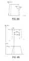
- FIGS. 2 (A), 2 (B) and 2 (C)are cross-sections, respectively depicting three operational modes of the non-volatile/floating gate transistor of FIG. 1;
- FIGS. 3 (A), 3 (B) and 3 (C)are cross-sections depicting the three operational modes of an alternative non-volatile/floating gate transistor to that of FIGS. 2 (A), 2 (B) and 2 (C);
- FIG. 4is a schematic diagram of a second embodiment of the present invention.
- FIG. 5 (A)is a cross-sectional view depicting part of the circuit of FIG. 4, and FIG. 5 (B) shows a timing diagram relating to one or more operational aspects of the embodiment of FIG. 4;
- FIGS. 6 (A) and 6 (B)are timing diagrams showing other operational aspects of the embodiment of FIG. 4;
- FIG. 7is a flow chart exemplifying one set of NV-RECALL operations for the embodiment of FIG. 4;
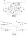
- FIG. 8is a schematic diagram of a third embodiment of the present invention.
- FIGS. 9 (A)- 9 (D)are a series of exclusive OR gates (XORs) useful in one embodiment of a NV-RECALL operation in which initially recalled data may be inverted.
- XORsexclusive OR gates
- FIG. 1shows a diagram of a non-volatile SRAM (NVSRAM) cell 100 in accordance with a preferred embodiment of the present invention.
- the cell 100generally comprises a gate 110 , a nonvolatile memory element (NVM) 120 coupled to the gate, and a static random access memory element (SRAM) 130 .
- Gate 110receives and/or provides one or more data signals and receives one or more control signals enabling (i) data to be read from or written to SRAM 130 , as well as (ii) operations affecting NVM 120 .
- NVM 120receives one or more control signals enabling programming, erasing and/or reading the NVM, and is configured to receive data from SRAM 130 .
- SRAM 130is configured to receive data from and/or provide data to input/output (I/O) busses (e.g., BL and BLB and/or circuitry coupled thereto) directly through gate 110 (e.g., through T 1 and T 2 ) and/or indirectly through NVM 120 (e.g., through FG 1 and S 1 ).
- I/Oinput/output
- gate 110may comprise first and second gate transistors T 1 and T 2 coupled to SRAM element 130 and receiving a first control signal (e.g., WL) at their gates, and a select transistor S 1 coupled to nonvolatile memory element 120 and receiving a second control signal (e.g., NVSEL) at its gate.
- first control signale.g., WL
- select transistor S 1coupled to nonvolatile memory element 120 and receiving a second control signal (e.g., NVSEL) at its gate.
- second gate transistor T 2may be absent.
- SRAM element 130may comprise first and second load transistors P 1 and P 2 , and first and second pulldown transistors N 1 and N 2 .
- the transistors P 1 , P 2 , N 1 and N 2may form a latch, but in alternative embodiments, load transistors P 1 and P 2 may be replaced with one or more resistors, or they may be completely absent (e.g., using a four_transistor SRAM cell such as that disclosed in U.S. Pat. No. 5,835,401; “A 16 Mb 400 MHz Loadless CMOS Four_transistor SRAM Macro,” ISSCC 2000, p.
- non-volatile memory element 120may comprise a floating gate transistor (e.g., FG 1 ), but may also comprise any type of readable and writable (or electrically erasable and programmable) nonvolatile transistor.
- FIGS. 2 (A)- 2 (C)show a cross-sectional view of FG 1 , in which the floating gate transistor is fabricated on a P-doped substrate.
- Conventional N + implantsmay form the source/drain terminals, and a conventional deep or directional N implant may form a “tip” implant at the source/drain terminal coupled to select transistor S 1 . This “tip” implant may be advantageous for electrically programming and/or erasing a FG transistor.
- the NV transistor (FG 1 )may further comprise (i) a floating gate (e.g., FG in FIGS. 2 (A)- 2 (C)), separated from the substrate by a gate oxide layer having a thickness of 20-150 ⁇ , preferably 50-100 ⁇ , and in one embodiment about 80 ⁇ , and (ii) a control gate (e.g., CG in FIGS. 2 (A)- 2 (C)), separated from the floating gate by an interpoly oxide layer having a thickness of 40-300 ⁇ , preferably 100-250 ⁇ , and in one embodiment about 180 ⁇ .
- a floating gatee.g., FG in FIGS. 2 (A)- 2 (C)
- a control gatee.g., CG in FIGS. 2 (A)- 2 (C)
- gate 110may comprise one or more pass gate transistors (e.g., T 1 and T 2 ), and NVM 120 may comprise select transistor S 1 in series with transistor FG 1 , as an additional, parallel path to the gate, between an I/O line (e.g., BL) and the SRAM 130 (and more specifically, node D 1 of the latch).
- the cell 100may thus be implemented as a compact SRAM cell with non-volatile (NV) shadow memory.
- This combination RAM-NVM cellmay be manufactured using conventional floating-gate of floating charge storage layer processing technologies.
- the non-volatility of this cellby which the data stored in SRAM cell 130 is saved in NVM 120 when it might otherwise be lost, may be achieved with only the transistor FG 1 , with a minimal use of extra control lines.
- the cell 100may thus be ideal for use in a data-save on power-down type application. A number of cells 100 may be combined to form an array.
- cell 100may thus comprise a conventional 6-transistor SRAM cell with the transistor FG 1 added for NVM storage and for recall.
- the select transistor S 1generally isolates the transistor FG 1 from the effects of the I/O line(s) (e.g., BL) and SRAM cell 130 during normal operation of the SRAM.
- a plurality of the present non-volatile SRAM cells, or a plurality of blocks of the non-volatile SRAM cellsmay form an array.
- the array, or any blocks thereofmay independently comprise a matrix of n by m cells, wherein n and m respectively designate the number of rows and columns of the array or block, and n and m are each independently an integer of at least 2, preferably at least 4, and more preferably at least 8.
- the array or block thereofmay have a maximum of about 20 megabits (20 Megs), preferably about 10 Megs, more preferably about 4 Megs.
- Table 1 belowshows the node voltages/data states for various modes of operation: NV-CLEAR, NV-STORE, NV-RECALL and normal volatile SRAM operation, where X denotes a Don't Care” state.
- Data and its complement (“datab”)are either VCC or 0 and are generally at opposite states.
- CG NVSEL WL BL BLB D1 D2 PG Vt COMMENT(S) NV-CLEAR VKN( ⁇ 7V >VCC 0V VCC X X low Volatile data not to ⁇ 12V) (to affected.
- CG and NVSEL pass voltagesmay be pulsed.
- VCCNVM may have I BET .
- CG voltagemay be pulsed.
- NV-RECALL, 0V 0V VCC 0V VCC 0V VCCmay be low Drop VARRAY below VCC cells pre- or high) just after writing 0's.
- VARRAY 0'smay be VCC.
- NV-READ Positive >VCC 0V VCC X data datab low (D1Recalled data true (not (NV-RECALL, bias > 0V) or high inverted).
- D1Recalled data true (not (NV-RECALL, bias > 0V) or high inverted).
- NV-CLEAR and NV-STORE operationsshow NV-CLEAR and NV-STORE operations, as well as two different NV-RECALL and NV-READ operations (one which writes all “0”s, providing “true” [non-inverted] data, but which includes, adjusting the supply voltage to the array; and one which writes all “1”s, providing inverted data, but which needs no array supply voltage adjustment).
- NV-STOREis preceeded by NV-CLEAR to ensure adequate margins (and thus success) for NV-STORE.
- the combination of NV-CLEAR and NV-STORE operationsmay be considered “programming” the NVM with the SRAM data.
- NV-RECALLdoes not have to be followed immediately by NV-CLEAR, but under certain conditions, or in certain embodiments, it may be advantageous to do so.
- the cell 100may comprise a six-transistor (6T) SRAM cell, which is fully symmetrical for conventional SRAM operations (e.g., READ and/or WRITE).
- 6Tsix-transistor
- the floating gate transistor FG 1is typically used only for NV-STORE and NV-RECALL operations.
- Soft NV-STOREe.g., independent of power decreases or failures
- “soft” NV-RECALL operationsare feasible, and may be controlled by conventional logic circuitry adapted to store and recall NV data in accordance with the description(s) herein.
- conventional power or voltage detection circuitrymay detect a power loss or power failure (or that such an event may be imminent). In any case, such power loss, power failure, detection thereof or detection that such event may be imminent may be considered to be a “power fail event”.
- a control signalmay be generated by such detection circuitry (which may further comprise conventional logic circuitry configured to generate such a signal), which in turn, will generate appropriate signals with appropriate digital or analog values to perform the NVM functions described herein.
- the first NVM function that occurs on detecting a “power-fail” event or conditionis clearing any data stored in the NVM (e.g., “NV-CLEAR”). This helps ensure that volatile data can be read from the SRAM element 130 and written into NVM element 120 using a minimal amount of power.
- the floating gate of FG 1is at a negative potential (e.g., about one-half of the voltage on the control gate) and the n+ diffusion on the bit line side (e.g., coupled to S 1 ) is at Vcc.
- the threshold voltage Vt of FG 1is then pulled low by discharge of electrons from the floating gate (FG) to the n+ diffusion common to it and select transistor S 1 .
- I BBTband to band tunneling current
- the control gate CGis at negative potential (e.g., VNN, which may be from about ⁇ 5V to about ⁇ 15V, preferably from about ⁇ 7V to about ⁇ 12V, and in one embodiment is about ⁇ 8V), and the transistor FG 1 is non-conducting. Therefore, the SRAM latched state is not disturbed by NV-CLEAR.
- an NV-CLEAR operationmay comprise applying a negative potential (VNN; e.g., any of the negative potentials described herein or a range such as ⁇ 7 to ⁇ 11V) to the control gate CG.
- VNNnegative potential
- the bit line voltage VBLand, optionally and independently, the complementary bit line voltage VBLB
- VCCvoltage
- the wordline voltage VWLmay move (or preferably be pulsed, optionally using a conventional charge pump circuit; see, e.g., CY refs: CD98018 and CD98019) to a positive potential>VCC to pass the supply voltage VCC to the source/drain terminal of FG 1 coupled to select transistor S 1 (i.e., opposite that source/drain terminal coupled to node D 1 of the SRAM latch).
- the NV-CLEAR operationmay apply such voltages to such nodes for a time ranging from 1 to 100 ms, preferably 1-10 ms, although it may be>100 ms or ⁇ 1 ms, as long as the conditions result in a low threshold voltage Vt for FG 1 .
- NV-STOREa programming operation, or as used herein, “NV-STORE”. NV-STORE operations may be initiated in at least two modes: (i) when a power loss or failure (or a condition indicating that such power loss or failure is imminent) is sensed, or (ii) when the current array data is to be stored, independent of power loss: or failure (e.g., a “soft” store).
- the latter modemay be particularly advantageous, in one example, when including the present NVSRAM array in a PLD (programmable logic device; e.g., a simple PLD [SPLD], complex PLD [CPLD], field programmable gate array [FPGA], etc.), a programmable clock generator, a microcontroller (e.g., a programmable general purpose microcontroller, a Universal Serial Bus microcontroller, etc.), a microprocessor or digital signal processor, etc.
- PLDprogrammable logic device
- SPLDsimple PLD
- CPLDcomplex PLD
- FPGAfield programmable gate array
- microcontrollere.g., a programmable general purpose microcontroller, a Universal Serial Bus microcontroller, etc.
- new programming or configuration informationmay be loaded or downloaded into the volatile memory for immediate use and fastest (down)loading speed, then stored in the nonvolatile memory at a more convenient time.
- the transistor S 1is off and the bit line BL is isolated from the transistor FG 1 .
- the control gate CG of transistor FG 1may be at a high positive potential Vpp. If D 1 is at 0V, the FG 1 channel is at 0V, and electrons are injected by Fowler-Nordheim (FN) tunneling (preferably uniform FN tunneling) from the channel into the floating gate (FG); and the Vt of transistor FG 1 goes high. If D 1 is at YCC, the potential difference between the channel which is at VCC and the FG is not high enough for any substantial electron injection, and Vt of FG 1 remains low.
- FNFowler-Nordheim
- control gate voltageVCG
- VNNnegative potential
- both of the transistors FG 1 and FG 2may be non-conducting and the SRAM latched state is not disturbed.
- the wordline voltage VWLis generally first brought to zero before the negative supply voltage VNN is removed.
- the regular SRAM Write/Read operationsare generally performed through the wordline voltage VWL, the bit line voltage VBL and the bit line voltage VBLB as indicated in TABLE 1.
- the time required for the NV-STORE operationis typically 1-20 msec, depending on the number of bits in the array, the supply voltage, the available maximum current, etc. Because NV-STORE may involve uniform FN tunneling, there may be no band-to-band (BTB) current, and in such a case, the power consumed is only the power used to charge up the floating gates (a negligible amount). Therefore, the NV-STORE operation in the present invention is ideal for the case of storing data in nonvolatile memory during power loss or failure.
- BTBband-to-band
- transistor FG 1since transistor S 1 is off, an inversion channel, created when the control gate voltage (VCG) is at VPP, is at the voltage present on node D 1 (VD 1 ).
- VGcontrol gate voltage
- VD 1VCC
- the threshold voltage Vt of the transistor FG 1generally remains low.
- NV-RECALL operationwhich may comprise a PRESET operation followed by a NV-READ operation, and which may be performed, for example, according to either of the two following methods:
- V A1is generally chosen to be sufficiently low that cells in which transistor FG 1 has a low threshold voltage (Vt low ) will overwrite a “1” that may be stored in the cell.
- VCCvoltage applied to CG
- VCCvoltage applied to CG
- the voltage at D 1 (0V)results from writing a “0” into the SRAM cell in the preceding step.
- the reference NVSRAM cell outputmay also be inverted.
- An XOR circuitmay now invert the recalled inverted state, leading to correct polarity.
- the supply voltage to the NVSRAM cell arraymay be decreased to weaken the latch so that the non-volatile data can be written into the SRAM, even at a typical end-of-life NVM charge retention state (e.g., 10 years or more).
- VARRAYheld at this low value, the bit line BL and the control gate CG are kept to VCC (not decreased) and, ideally, the signal NVSEL is taken sufficiently above VCC to enable passing VCC from BL to FG 1 , but not so much above VCC to risk breakdown of the select transistor gate oxide.
- VARRAYis decreased to a worst case maximum value of the PMOS and/or NMOS thresholds in the SRAM element, so that volatile data may be written from the non-volatile transistor and/or held (however weakly, either without overwriting or once written from NVM).
- a threshold mismatchmay advantageously allow data to be maintained by the MOS devices (which may be a slight weak-inversion) even if VARRAY decreases below the worst case maximum value of the SRAM transistor thresholds.
- the control gate CGmay also be taken to a non-VCC value, depending on the end-of-life characteristic requirements of the non-volatile floating gate FG 1 .
- NVSRAM cell 100may replace the select transistor S 1 with a PMOS transistor.
- the voltage on node NVSELmay be changed as follows while all other signals are same as in TABLE 1.
- an external supply voltage supporte.g., a battery
- a CLEAR cycleis executed just after a RECALL cycle, a power decrease or failure may interrupt the CLEAR process, and data in NVM could be lost. Under these circumstances, a CLEAR cycle would generally have to be complete before a NV-STORE operation takes place to re-capture the data, and an external battery may supply sufficient power to enable
- the cell 100does normally consumes little or no additional power during the NV-CLEAR and/or NV-STORE cycles.
- the cleared statewill not be disturbed by the volatile data, and may be supported when the volatile data is in a particular state (e.g., a D 1 “logic high” state).
- the programmed statemay suffer some risks due to potential SRAM data disturbance, depending on the technology and the VCC supply voltage level.
- Threshold voltage disturbancesmay be controlled by applying a predetermined bias voltage on the control gate CG (which is preferably one that, in the example of FIG. 1, maintains FG 1 in a non-conducting state) and by selecting a minimal voltage supply to the array.
- the NVMmay be programmed (i) the first time the cell 100 is powered up and (ii) after each NV-RECALL cycle.
- Switching of the state of latchdraws a current through VARRAY.
- recall operationsmay be done on selected groups of word lines sequentially, instead of on the whole array simultaneously.
- Vt disturbances of the NV transistor FG 1 by the potential at node D 1can be minimized by a careful choice of bias (e.g., between 0 to Vcc) on the control gate CG so that the FG 1 Vt can meet the end of life characteristic requirements for either Vt low (an NV-CLEARed state) or Vt high (NV-STOREd state).
- biase.g., between 0 to Vcc
- the NV-CLEARed stateshould be supported for NVM “end-of-life” conditions.
- the NV transistor shown in FIG. 2is shown as an n-channel floating gate transistor that uses FN tunneling for NV-CLEAR and NV-STORE operations to put its Vt in low and high values, respectively.
- the NV transistorcan also be a p-channel floating gate transistor, fabricated in an N-well, as depicted in FIG. 3 .
- NV-CLEARelectrons may be injected into the floating gate by band to band tunneling (BBT).
- BBTband to band tunneling
- node D 1is at VCC, then electrons would be discharged to the N-well by FN tunneling, making the Vt of the p-channel floating gate transistor negative or non-conducting.
- a high threshold voltage Vtmay be achieved by hot electron injection into the floating gate due to BBT.
- Discharge of electronsmay be achieved by FN tunneling.
- the 8T NVSRAM 100 of FIG. 1may be functionally replaced by 7T NVSRAM cell 200 .
- the 7T NVSRAM cell 200comprises a gate 210 , a nonvolatile memory element (NVM) 220 coupled to the gate, and a static random access memory element (SRAM) 230 , just as for the 8T PNVSRAM 100 of FIG. 1 .
- the primary difference between 7T NVSRAM cell 200 and 8T NVSRAM cell 100is that gate 210 has one less transistor than gate 110 (or, alternatively, that NVM 220 is not directly coupled to I/O line BL and has one less transistor than NVM 120 ).
- bit line BLmay be connected to D 1 through a series combination of pass transistor T 11 and floating gate transistor FG 11 , configured such that this series combination is approximately equivalent to the transistor T 1 of cell 100 during conventional SRAM READ/WRITE operations, but is equivalent to the series combination of select transistor S 2 and floating gate transistor FG 1 of cell 100 during NVM operations.
- While the 8T NVSRAM cell 100 of FIG. 1may be coupled to a single word line, the 7T NVSRAM cell 200 of FIG. 4 may be coupled to divided first and second SRAM word lines (e.g., WL 1 and WL 2 ).
- cell 200stores data from SRAM cell 230 into NVM 220 on a “power fail” condition and recalls the data from NVN 220 back into SRAM 230 when power is reapplied (a so-called “power-up” condition).
- floating gate transistor FG 11is generally in series with the pass transistor T 11 .
- NV-CLEARwhich may be done upon power loss and which generally is performed after each recall (and generally prior to normal SRAN operations), brings the Vt of FG 11 low and enables fast, efficient SRAM READ and WRITE operations in all cells.
- the description of the other operations of the cell 200may be similar to those of the cell 100 , including decreasing VARRAY during recall.
- the bias on the control gate CG during SRAM READ and WRITE operationsis at least about VCC, and preferably is about VCC (to minimize power consumption).
- Performing NV-CLEAR after NV-RECALLalso ensures that the array data can be stored in the NVM elements at the next “power-fail” event.
- the threshold voltage Vt of the floating gate transistor FG 11may be lowered to a low value (e.g., less than or equal to about 0V).
- electronsmay be removed from the floating gate of FG 11 , which may be at a negative potential compared to the node VBL 1 , which will generally be about or above VCC.
- VBLBL
- WL 1VWL 1
- VCCvoltage of a PMOS or NMOS transistor
- Nis a number of from 1 to 4, more preferably from 1.2 to 2.5
- T 11can pass a voltage of from VCC to VBL to FG 11 , thereby providing a source of band-to-band tunneling current for FN programming of FG 11 .
- the voltage on WL 2is held to about 0V, and the transistor T 12 is thus off (or non-conducting).
- FIG. 5 (A)A cross-sectional view depicting the removal of electrons from FG 11 is shown in FIG. 5 (A), and timing diagrams relating to the NV-CLEAR operation for cell 200 are shown in FIG. 5 (B).
- the threshold voltage Vt of FG 1is preferably at a low state, so that FG 11 will be in a strong conduction state when the control gate voltage is at VCC (for subsequent SRAM READ/WRITE operations). Furthermore, when the FG 11 Vt is low, the drain to source voltage (VDS) of FG 11 will also be low.
- the transistor T 11is generally turned on by applying a clearing voltage (VWCLR) to the word line WL 1 .
- the clearing voltage on word line WL 1is sufficiently greater than VCC to pass the voltage from input/output (I/O) line BL, which is generally about or slightly above VCC, to the n+ diffusion of the floating gate transistor (see, e.g., VBL 1 in FIG. 5 (A)).
- the voltages in excess of VCC(e.g., on word line WL 1 and/or bit line BL) may be provided by a conventional charge pump.
- a bit line voltage higher than VCCmay enable a faster clear, or alternatively, a less negative voltage VNN on the control gate.
- a combination of positive voltage on the n+ diffusion and a negative voltage on the floating gatemay increase the n+ to leakage current due to band to band tunneling (“I BBT ” in FIG. 5 (A)), which can occur when VCC is at its nominal value.
- the sum of all I BBT 's for the arraymay be reduced by (i) implementing a slow ramp (rate of change) of Vnn and/or the voltages on BL or WL 1 , and/or (ii) partitioning the array (or portion thereof to be cleared) into sub-blocks by applying VWCLR to selected groups of the word lines WL 1 .
- FIG. 5An exemplary timing sequence of the various voltages and/or pulses applied to the cell 200 in order to clear NVM 220 is shown in FIG. 5 (B).
- the voltages on BL and WL 1are raised at substantially the same time, and thus, a single control signal may initiate these sub-operations.
- the negative pulsegenerally applied to Vcg (assuming FG 11 is an n-channel transistor; a positive overvoltage is applied when FG 11 is a p-channel device, see FIG.
- timing of the three signals/pulsesmust be arranged such that their pulse widths (t pw ) overlap at their effective voltages for a length of time effective to clear the NVM or substantially remove the electrons from the floating gate or charge storage layer of the NV transistor.
- this length of timeis on the order of 1 ms (e.g., from 100 ns to 10 ms, preferably from about 500 ns to about 5 ms).
- standard SRAM READ/WRITE operationsmay be performed by setting the voltage on the FG 11 control gate (VCG) to about, equal to or greater than VCC. Since FG 11 will generally be conducting strongly in this operational mode, the drain to source voltage drop (Vds) across the floating gate transistor channel will generally be quite small, and the effect of FG 11 on SPAM cell operations should be minimal.
- the width-to-length ratio W/L of pass transistor T 11may be larger than the width-to-length ratio W/L of pass transistor T 12 to minimize the FG 11 Vds effect on the operation of the cell 100 .
- the (drain) disturbis generally minimal since VCG should also be at or about VCC.
- an NV-STORE operationmay save the volatile data in SRAM 230 (which would otherwise be lost) in NVM 220 .
- NV-STOREmay comprise turning off the gate transistor to the true data I/O line (e.g., T 11 ), for example by setting the corresponding word line (e.g., WL 1 ) voltage to 0V.
- VCGmay be raised or pulsed to a positive overvoltage Vpp (e.g., from about 12V to about 18V, and in one embodiment, about 15V) for a time of from approximately 0.1 to 100 ms, preferably from about 1 to about 10 ms.
- VCGmay be lowered to a negative “overvoltage” (e.g., Vnn), as shown in FIG. 3 (B).
- VCGthe control voltage VCG during SRAM READ/WRITE operations.
- the inversion channel under the floating gatewill generally be at the supply voltage VCC.
- the voltage difference between the floating gate and the channelis generally insufficient for substantial FN tunneling, and the Vt of the floating gate transistors connected to the SRAM cells storing a 1 generally remain low (i.e., Vt low , which in one embodiment is about 0V).
- NV-STOREis an extremely low power operation, which may be important when an impending power failure is sensed. For increase the likelihood of success, NV-STORE generally consumes a minimum amount of power.
- V ARRAYThe array voltage
- VCC NOMthe nominal value of VCC
- Such pumpingmay be desirable to inhibit FN tunneling of the NVM cells in a 1 state.
- NV-RECALLmay be conducted by the following sequence, illustrated by the waveforms in FIGS. 6 (A)-(B):
- V ARRAYvoltage ⁇ VCC
- VCCvoltage translation or reduction circuitry
- FIG. 6 (A)shows a timing diagram for the WL 2 and BLB pulses when writing a “0” to SRAM cell 230 .
- the voltage at node D 1is now about 0V and the voltage at node D 2 is now about the same as the value of V ARRAY .
- the WL 2 voltagemay be brought down to 0, as shown in FIG. 6 (A).
- Vcg to Vcg RAMpreferably a value of from [0.9 ⁇ VCC] to [1.1 ⁇ VCC], or about VCC
- a short time thereaftere.g., a time sufficient to enable the data in NVM 220 to write itself into SRAM 230 , which in certain embodiments may be from about 0.5 to 1000 ns (preferably from 1 to 200 ns, more preferably from 10 to 100 ns), raise WL 1 to VCC, for a length of time t pulse .
- the FG 11 Vtwill be low, VCC (or slightly less than VCC) from BL is passed to D 1 , and the SRAM cell 230 switches to a “1 state.
- the FG 11 Vtis high, and no voltage from BL will generally be passed into the SRAM cell 230 , thereby maintaining a “0” in SRAM cell 230 (consistent with the example shown in FIGS. 6 (A)-(B)).
- the time t pulseis generally selected to be that length of time that is sufficient to switch the SRAM cell 230 in a cell 200 having a Vt low NV transistor from a preset “0” to a “1 state, but insufficient to switch the SRAM cell 230 in a cell 200 having a Vt high NV transistor from a preset “0” to a state “1.
- VCGmay be lowered below VCC to make sure that the NV transistor leakage in the Vt high state is low enough that cells at a “0 state are not erroneously switched to a “1 state.
- NV-RECALLmay be performed in a few ns (e.g., 1-10, preferably 2-5 ns) for a block of NVSRAM cells.
- the arraymay be subdivided into blocks, then a separate and/or independent NV-RECALL operations (PRESET and/or NV-READ) performed on each block.
- the blocksneed not be equal in size because Icc may be higher when WL 1 is at VCC (as compared to when WL 2 is at VCC). Therefore, a block of WL 2 s may be selected for PRESET that is larger than the block of WL 1 s that are selected for the corresponding NV-READ.
- V ARRAYis generally ⁇ VCC to enable SRAM cells to switch to a “1 state when: (i) PRESET has written all 0's into the SRAM cells, (ii) BL is at or about VCC, and (iii) FG 11 is conducting.
- pulldown transistors N 11 and N 12may independently have a larger drive capability (e.g., W/L) than the corresponding pass transistors T 12 and T 11 .
- the n-well enclosing the PMOS transistors P 11 and P 12is generally biased at or about VCC to prevent forward biasing the P + /n-well drain junctions of the transistors P 11 and P 12 .
- V ARRAYis generally ramped from V A1 to VCC.
- the followingmay summarize key aspects of the NV-RECALL operation, in particular for the cell 200 of FIG. 4 and the case where all SRAM cells 230 are PRESET to a digital logic “0”:
- V ARRAYV A1 , where V A1 is kept low ( ⁇ VCC), but high enough for data retention.
- the cells 200 which stored a “1 during NV-STOREwill have a conducting floating gate transistor FG 11 (and transistor T 11 ).
- SRAM 230may be switched to a “1 state, but where the voltage at D 1 is generally about V ARRAY .
- an alternative NV-RECALL operationpresets all SRAM cells 230 to a digital logic “1” prior to NV-READ.
- This alternative methodmay be preferred when pullup PMOS transistors P 11 and/or P 12 are weak (e.g., small current drive relative to gate transistor T 11 and/or pulldown NMOS transistors N 11 and/or N 12 ). In such a case, it is generally easier to pull down D 1 towards 0V through T 11 and FG 11 .
- NV-CLEAR and NV-STOREmay be as previously described, but V ARRAY may be about or equal to VCC during
- NV-CLEAR VNN( ⁇ 7V >VCC 0V ⁇ VCC 0V data datab low All FG Vt's set low by to ⁇ 12V pulse FN tunneling. pulse)
- FIG. 7shows two methods of re-inverting the recalled inverted data, one of which was described generally for NVSRAM cell 100 , and one which now will be described for NVSRAM cell 200 .
- any method of data inversion that works under the operational conditions of the integrated circuit containing the present NVSRAM arraywill be acceptable.
- NV-CLEARsets the FG 11 Vt low.
- a “dummy” NV-STORE operationmaintains a low FG 11 Vt for those cells in which the inverted SRAM data is a digital “1”, and changes the FG 11 Vt to high if the inverted SRAM data is a digital “0.”
- NV-RECALLthen comprises PRESETting all SRAM cells to a digital “1”, then NV-READing the cells to re-invert the data therein.
- the integrated circuitmay have two output paths from the sense amplifiers receiving data signals from particular columns, or blocks of columns, in the array.
- One output pathincludes an inverting output buffer (e.g., for data inversion after NV-READ), and the other includes a non-inverting buffer (e.g., for normal SRAM operations).
- Appropriate logic circuitrye.g., a switch or mux toggles between these paths, depending on the operation being performed.
- An alternate embodiment of the 7T NVSRAM cell 200is one in which the NMOS pass transistors T 11 and T 12 are replaced by PMOS transistors.
- the N-channel FG transistor FG 11may be replaced by a P-channel FG transistor, like that shown in FIG. 3 .
- the operation of the alternative 7T NVSRAM cell with a P-channel FG transistorwould be similar to the one with the N-channel FG transistor, but for appropriate changes in the BL voltages for the p-channel floating gate transistor operation (see, e.g., Table 2 above).
- the band widths, or margins for error, when transferring data between NVM and SRAM elements in the present inventionis remarkably large, compared to conventional “shadow” NVM that communicates with a corresponding SRAM through a bus. This relatively large margin becomes particularly important when transferring data upon a power loss or failure.
- NVSRAM cell 300is similar to NVSRAM cell 200 , except for an extra NV transistor between gate transistor T 22 and the SRAM cell (latch) 330 , and one less word line to control transistors in gate 310 .
- One advantage of the cell 300is the addition of only one global control signal VCG and two floating gate transistors FG 1 and FG 2 to a conventional 6T SRAM cell.
- NV-CLEAR, NV-STORE and NV-RECALL operationsare quite similar to those of the other NVSRAM cells described herein, and may be summarized in TABLE 5 below.
- Vt1(of Vt2 (of Mode Vcg WL BL BLB D1 D2 FG1) FG2) Comment(s)
- Low Low VNNcomprises pulse of ⁇ 10 ms.
- FG CLEARe.g., (pulse) Vt pulled low ( ⁇ 0V or less) by ⁇ 7V to FN tunneling from negative FG to ⁇ 12V) positively biased drain.
- SRAM VCC VCC data databdata datab Low Low Normal SRAM operation
- WRITE/ READ NV- VPP 0V X X VCC 0V Low High VPPcomprises pulse of ⁇ 1 ms.
- STOREe.g., High FG Vt ( ⁇ VCC) by FN (“1”) 12- tunneling of electrons to FG. 18V
- STORE (“0”)NV- VCC VCC VCC VCC 0V Low High Generally followed by NV-CLEAR.
- RECALL (“1”)NV- VCC VCC VCC VCC 0V VCC High Low Generally followed by NV-CLEAR. RECALL (“0”)
- NVSRAM cell 300is the addition of only one global control signal VCG and two floating gate transistors FG 1 and FG 2 . Several differences in the operation of NVSRAM cell 300 should be noted.
- both I/O lines(BL and BLB) are raised to VCC.
- Vcgis at VNN, both NV transistors are non-conducting, and any data in SRAM 330 will not be disturbed.
- it may be advantageous to first turn off the gate transistorse.g., bring WL to 0V for the circuit in FIG. 8) before removing VNN from Vcg.
- one NV transistorAfter NV-STORE and during NV-RECALL, one NV transistor will have a high Vt, while the other will have a low Vt. This may help improve the stability of the data transferred back into SRAM 330 from NVM 320 , relative to 7T NVSRAM cell 200 .
- the general objective of the NV-RECALL operationis to restore the state of the SRAM array (e.g., the latched data) that was saved during the NV-STORE operation.
- the operationmay have the following sequence:
- Vt of FG 1e.g., Vt 1
- VCC on BLis passed to D 1 .
- the Vt of FG 2e.g., Vt 2
- VCC from BLBis not passed to D 2 .
- the SRAM latchnow has a “1” state, and the SRAM data has been restored.
- the recall operationis generally performed after power up following a power fail or to restore the saved SRAM state.
- NVSRAM cell 300may include p-channel gate transistors, in which case the array oerations are as shown in Table 6 below.
- Vt1(of Vt2 (of Mode Vcg WL BL BLB D1 D2 FG1) FG2) Comment(s)
- NV- VNN 0V VCC VCC data datab Low Low VNNcomprises pulse of ⁇ 0.1- CLEAR (e.g., 10 ms. FG Vt pulled low ( ⁇ 0V or ⁇ 7V to less).
- CLEARe.g. 10 ms.
- FG Vt pulled low⁇ 0V or ⁇ 7V to less.
- SRAM VCC 0V data data databdata datab Low Low Normal SRAM operation WRITE/ READ NV- VPP VCC VCC VCC 0V Low High Unbalanced FG Vt's.
- STOREe.g., (“1”) 12- 18V
- NV- VCC VCC VCC 0V VCC High Low STORE(“0”)
- NV- VCC 0V VCC VCC VCC 0V Low High Generally followed by NV-CLEAR(“1”)
- NV- VCC VCC VCC 0V VCC High Low Generally followed by NV-CLEAR(“0”)
Landscapes
- Static Random-Access Memory (AREA)
Abstract
Description
| TABLE 1 | |||||||||||
| Operation | CG | NVSEL | WL | BL | BLB | D1 | D2 | PG Vt | COMMENT(S) | ||
| NV-CLEAR | VKN (−7V | > | 0V | VCC | X | X | X | low | Volatile data not | ||
| to −12V) | (to | affected. CG and NVSEL | |||||||||
| pass | voltages may be pulsed. | ||||||||||
| VCC) | NVM may have IBET. | ||||||||||
| NV-STORE | VPP (12- | 0V | X | X | data | datab | low (D1 = | If D1 = 0V, then FN | |||
| 20V; | VCC) or high | tunneling; if D1 = VCC, | |||||||||
| −15V) | (D2 = VCC) | no tunneling. CG | |||||||||
| voltage may be pulsed. | |||||||||||
| NV-RECALL, | 0V | 0V | VCC | 0V | VCC | (may be low | Drop VARRAY below VCC | ||||
| cells pre- | or high) | just after writing 1's | |||||||||
| set to all | to minimize current | ||||||||||
| 1's | throughput | ||||||||||
| NV-READ | VCC | 0V | 0V | X | datab | data | low (D1 = | ||||
| (NV-RECALL, | VCC) or high | natural (unprogrammed) | |||||||||
| all 1's) | (D2 = VCC) | threshold of FG1. | |||||||||
| Recalled data inverted. | |||||||||||
| Raise VARRAY to VCC | |||||||||||
| after READ. | |||||||||||
| NV-RECALL, | 0V | 0V | VCC | 0V | VCC | (may be low | Drop VARRAY below VCC | ||||
| cells pre- | or high) | just after writing 0's. | |||||||||
| set to all | Alternatively, | ||||||||||
| 0's | may = VCC. | ||||||||||
| NV-READ | Positive | > | 0V | VCC | X | data | datab | low (D1 = | Recalled data true (not | ||
| (NV-RECALL, | bias > | 0V) or high | inverted). Raise VARRAY | ||||||||
| all 0's) | bias 1 | (D2 = 0V) | to VCC after READ (if | ||||||||
| necessary). | |||||||||||
| SRAM WRITE/ | From | VCC | VCC | 0V or | 0V or | low | Normal SRAM operation. | ||||
| READ | to VCC | or 0V | VCC | or 0V | VCC | ||||||
| TABLE 2 | ||
| Voltage at NVSEL | ||
| Operation | (S1 = PMOS) | Comment(s) |
| NV- | 0 | To pass VBL ≧ VCC |
| to N+of FG1 to | ||
| lower FG Vt. | ||
| SRAM WRITE/READ | VCC | To isolate the FG |
| transistor. | ||
| NV-STORE | VCC | To isolate FG1 from |
| VBL. | ||
| NV- | VCC | Turn off S1; T1 and |
| (WRITE 0's) | T2 conducting. | |
| NV READ (NV- | 0 | Couple VBL ≧ VCC |
| METHOD 1) | to FG1 | |
| NV-RECALL METHOD 2 | VCC | Turn off S1; Write |
| ( | thru T1 and T2 | |
| NV READ (NV- | 0 | Couple VBL = 0 to |
| METHOD 2) | FG1 (connect). | |
| TABLE 3 | |||||||||||
| Vt of | |||||||||||
| Mode | Vcg | WL1 | WL2 | BL | BLB | D1 | D2 | FG11 | Comment(s) | ||
| NV-CLEAR | −7 ≦ VNN ≦ | >VCC | 0V | ≧VCC | 0V | data | datab | Low | WL voltage may be pulsed. | ||
| −12V, 0.1- | Program FG Vt's to low | ||||||||||
| 100 ms) | state (<<VCC or <0V). | ||||||||||
| SRAM WRITE | ≧VCC | VCC | VCC | −VCC/2 | −VCC/2 | data | datab | Low | FG11 strongly conducting; | ||
| to | to | NVSRAM cell operates as | |||||||||
| VCC−Vt | VCC−Vt | conventional SRAM cell. | |||||||||
| SRAM READ | ≧VCC | VCC | VCC | −VCC/2 | −VCC/2 | data | datab | Low | |||
| to | to | ||||||||||
| VCC−Vt | VCC−Vt | ||||||||||
| NV-STORE | Vpp (12- | 0V | X | VCC | 0V | Low | Preceded by NV-CLEAR. | ||||
| (“1”) | 18V, 0.1- | ||||||||||
| 100 ms) | |||||||||||
| NV-STORE | Vpp (12- | X | X | 0V | VCC | High | Preceded by NV-CLEAR. | ||||
| (“0”) | 18V, 0.1- | ||||||||||
| 100 s) | |||||||||||
| NV-RECALL, | 0V | 0V | VCC | VCC | Low | 0's written into all | |||||
| step | |||||||||||
| 1 | or | cells, ≦10 ns. | |||||||||
| High | |||||||||||
| NV-RECALL, | 0V | VCC | 0V | data | datab | Low | SRAM array restored to | ||||
| step 2 | or | state at time of NV-STORE | |||||||||
| High | |||||||||||
| TABLE 4 | |||||||||||
| Mode | Vcg | WL1 | WL2 | BL | BLB | D1 | D2 | FG Vt | Comment(s) | ||
| NV-CLEAR | VNN (−7V | >VCC | 0V | ≧VCC | 0V | data | datab | low | All FG Vt's set low by | ||
| to −12V | pulse | FN tunneling. | |||||||||
| pulse) | |||||||||||
| NV- | Vpp | 0V | 0V | X | X | data | datab | low or | FG Vt = low if data = 1 | ||
| pulse | high | ||||||||||
| PRESET | VCC | 0V | VCC | 0V | low or | D1 = VCC for all cells. | |||||
| ALL 1's | high | FG Vt set by NV-STORE. | |||||||||
| NV | VCC | 0V | 0V | VCC | datab | data | low or | FG Vt set by NV-STORE. | |||
| (for NV- | high | Cells are restored to | |||||||||
| RECALL) | state complementary to | ||||||||||
| NV-STORE state. | |||||||||||
| TABLE 5 | ||||||||||
| Vt1 (of | Vt2 (of | |||||||||
| Mode | Vcg | WL | BL | BLB | D1 | D2 | FG1) | FG2) | Comment(s) | |
| NV- | VNN | VCC+Vt | VCC | VCC | data | datab | Low | Low | VNN comprises pulse of −10 ms. FG | |
| CLEAR | (e.g., | (pulse) | Vt pulled low (−0V or less) by | |||||||
| −7V to | FN tunneling from negative FG to | |||||||||
| −12V) | positively biased drain. | |||||||||
| Follows power up and every NV- | ||||||||||
| RECALL. | ||||||||||
| SRAM | VCC | VCC | data | datab | data | datab | Low | Low | Normal SRAM operation | |
| WRITE/ | ||||||||||
| READ | ||||||||||
| NV- | 0V | X | VCC | 0V | Low | High | VPP comprises pulse of −1 ms. | |||
| STORE | (e.g., | High FG Vt (−VCC) by FN | ||||||||
| (“1”) | 12- | tunneling of electrons to FG. | ||||||||
| 18V) | No FN tunneling when channel is | |||||||||
| NV- | X | X | 0V | VCC | High | Low | at VCC. | |||
| STORE | ||||||||||
| (“0”) | ||||||||||
| NV- | VCC | VCC | VCC | VCC | 0V | Low | High | Generally followed by NV-CLEAR. | ||
| RECALL | ||||||||||
| (“1”) | ||||||||||
| NV- | VCC | VCC | VCC | 0V | VCC | High | Low | Generally followed by NV-CLEAR. | ||
| RECALL | ||||||||||
| (“0”) | ||||||||||
| TABLE 6 | ||||||||||
| Vt1 (of | Vt2 (of | |||||||||
| Mode | Vcg | WL | BL | BLB | D1 | D2 | FG1) | FG2) | Comment(s) | |
| NV- | 0V | VCC | VCC | data | datab | Low | Low | VNN comprises pulse of −0.1- | ||
| CLEAR | (e.g., | 10 ms. FG Vt pulled low (−0V or | ||||||||
| −7V to | less). Follows power up and | |||||||||
| −11V) | every NV-RECALL. | |||||||||
| VCC | 0V | data | datab | data | datab | Low | Low | Normal SRAM operation | ||
| WRITE/ | ||||||||||
| READ | ||||||||||
| NV- | VPP | VCC | VCC | VCC | 0V | Low | High | Unbalanced FG Vt's. | ||
| STORE | (e.g., | |||||||||
| (“1”) | 12- | |||||||||
| 18V) | ||||||||||
| NV- | VCC | VCC | 0V | VCC | High | Low | ||||
| STORE | ||||||||||
| (“0”) | ||||||||||
| NV- | 0V | VCC | VCC | 0V | Low | High | Generally followed by NV-CLEAR. | |||
| RECALL | ||||||||||
| (“1”) | ||||||||||
| NV- | VCC | VCC | VCC | 0V | VCC | High | Low | Generally followed by NV-CLEAR. | ||
| RECALL | ||||||||||
| (“0”) | ||||||||||
Claims (17)
Priority Applications (1)
| Application Number | Priority Date | Filing Date | Title |
|---|---|---|---|
| US09/871,172US6556487B1 (en) | 2000-09-20 | 2001-05-31 | Non-volatile static memory cell |
Applications Claiming Priority (2)
| Application Number | Priority Date | Filing Date | Title |
|---|---|---|---|
| US23395700P | 2000-09-20 | 2000-09-20 | |
| US09/871,172US6556487B1 (en) | 2000-09-20 | 2001-05-31 | Non-volatile static memory cell |
Publications (1)
| Publication Number | Publication Date |
|---|---|
| US6556487B1true US6556487B1 (en) | 2003-04-29 |
Family
ID=26927409
Family Applications (1)
| Application Number | Title | Priority Date | Filing Date |
|---|---|---|---|
| US09/871,172Expired - LifetimeUS6556487B1 (en) | 2000-09-20 | 2001-05-31 | Non-volatile static memory cell |
Country Status (1)
| Country | Link |
|---|---|
| US (1) | US6556487B1 (en) |
Cited By (62)
| Publication number | Priority date | Publication date | Assignee | Title |
|---|---|---|---|---|
| US20020184574A1 (en)* | 2001-05-31 | 2002-12-05 | Mackey Richard P. | Power loss memory back-up |
| US20030128595A1 (en)* | 2001-12-21 | 2003-07-10 | Marr Ken W. | Sram power-up system and method |
| US20030223288A1 (en)* | 2002-03-19 | 2003-12-04 | O2Ic, Inc. | Non-volatile memory device |
| US20030231528A1 (en)* | 2002-03-19 | 2003-12-18 | 021C, Inc. | Non-volatile differential dynamic random access memory |
| US20040001373A1 (en)* | 2002-06-28 | 2004-01-01 | Shion-Hau Liaw | Non-volatile SRAM cell |
| US20040090257A1 (en)* | 2002-11-08 | 2004-05-13 | International Business Machines Corporation | Low power overdriven pass gate latch |
| US6798008B2 (en) | 2002-03-19 | 2004-09-28 | 02Ic, Inc. | Non-volatile dynamic random access memory |
| US20050141272A1 (en)* | 2003-12-31 | 2005-06-30 | Dongbuanam Semiconductor Inc. | Non-volatile memory device and drive method thereof |
| US20050170586A1 (en)* | 2004-01-29 | 2005-08-04 | O2Ic, Inc., (A California Corporation) | Method of manufacturing non-volatile DRAM |
| US20050174842A1 (en)* | 2004-02-11 | 2005-08-11 | Nantero, Inc. | EEPROMS using carbon nanotubes for cell storage |
| US20050219913A1 (en)* | 2004-04-06 | 2005-10-06 | O2Ic, Inc. | Non-volatile memory array |
| US6965524B2 (en)* | 2002-03-19 | 2005-11-15 | O2Ic, Inc. | Non-volatile static random access memory |
| US20060007772A1 (en)* | 2002-03-19 | 2006-01-12 | O2Ic, Inc. | Non-volatile memory device |
| US20060114020A1 (en)* | 2004-09-24 | 2006-06-01 | Cypress Semiconductor Corporation | One time programmable latch and method |
| US20060193174A1 (en)* | 2005-02-25 | 2006-08-31 | O2Ic | Non-volatile and static random access memory cells sharing the same bitlines |
| US20060268615A1 (en)* | 2005-05-30 | 2006-11-30 | Hynix Semiconductor Inc. | Nonvolatile semiconductor static random access memory device |
| US7186612B2 (en) | 2004-01-28 | 2007-03-06 | O2Ic, Inc. | Non-volatile DRAM and a method of making thereof |
| US7232717B1 (en) | 2002-05-28 | 2007-06-19 | O2Ic, Inc. | Method of manufacturing non-volatile DRAM |
| US20070165445A1 (en)* | 2006-01-18 | 2007-07-19 | International Business Machines Corporation | Eight transistor SRAM cell with improved stability requiring only one word line |
| US20070242514A1 (en)* | 2005-03-10 | 2007-10-18 | O2Ic, Inc. | NAND-structured nonvolatile memory cell |
| US7339848B1 (en) | 2005-11-03 | 2008-03-04 | Cypress Semiconductor Corporation | Anti-fuse latch circuit and method including self-test |
| US20080137440A1 (en)* | 2006-12-07 | 2008-06-12 | Taiwan Semiconductor Manufacturing Co., Ltd. | SRAM cell with separate read and write ports |
| US20080151605A1 (en)* | 2006-07-06 | 2008-06-26 | Stmicroelectronics Pvt. Ltd. | 8-T SRAM cell circuit, system and method for low leakage current |
| US7426142B1 (en) | 2005-05-05 | 2008-09-16 | Cypress Semiconductor Corporation | Device and method for sensing programming status of non-volatile memory elements |
| US20090168520A1 (en)* | 2007-12-31 | 2009-07-02 | Simtek | 3T high density NVDRAM cell |
| US20090168521A1 (en)* | 2007-12-31 | 2009-07-02 | Simtek | 5T high density NVDRAM cell |
| US20090168519A1 (en)* | 2007-12-31 | 2009-07-02 | Simtek | Architecture of a nvDRAM array and its sense regime |
| US7821859B1 (en) | 2006-10-24 | 2010-10-26 | Cypress Semiconductor Corporation | Adaptive current sense amplifier with direct array access capability |
| US7859906B1 (en) | 2007-03-30 | 2010-12-28 | Cypress Semiconductor Corporation | Circuit and method to increase read margin in non-volatile memories using a differential sensing circuit |
| US7859925B1 (en) | 2006-03-31 | 2010-12-28 | Cypress Semiconductor Corporation | Anti-fuse latch self-test circuit and method |
| US20110188296A1 (en)* | 2007-06-29 | 2011-08-04 | Semiconductor Energy Laboratory Co., Ltd. | Semiconductor Memory Device and Semiconductor Device |
| US8072834B2 (en) | 2005-08-25 | 2011-12-06 | Cypress Semiconductor Corporation | Line driver circuit and method with standby mode of operation |
| US20120320658A1 (en)* | 2011-06-15 | 2012-12-20 | Industrial Technology Research Institute | Nonvolatile static random access memory cell and memory circuit |
| US20130039127A1 (en)* | 2011-08-09 | 2013-02-14 | Flash Silicon Incorporation | Non-volatile static random access memory devices and methods of operations |
| US8467243B1 (en)* | 2009-09-28 | 2013-06-18 | Cypress Semiconductor Corporation | nvSRAM with inverted recall |
| US8537597B2 (en)* | 2011-11-30 | 2013-09-17 | Kabushiki Kaisha Toshiba | Semiconductor memory device |
| US20130294161A1 (en)* | 2012-05-07 | 2013-11-07 | Aplus Flash Technology, Inc. | Low-voltage fast-write nvsram cell |
| US20130308399A1 (en)* | 2012-05-18 | 2013-11-21 | Stmicroelectronics Pvt. Ltd. | Write self timing circuitry for self-timed memory |
| US20140119118A1 (en)* | 2012-10-26 | 2014-05-01 | Aplus Flash Technology, Inc. | 8t nvsram cell and cell operations |
| US20140177348A1 (en)* | 2012-12-21 | 2014-06-26 | Flashsilicon Incorporation | Non-volatile register and non-volatile shift register |
| TWI450272B (en)* | 2006-07-13 | 2014-08-21 | Atmel Corp | High-voltage cmos latch for non-volatile memory and method therefor |
| US8854901B2 (en) | 2012-05-18 | 2014-10-07 | Stmicroelectronics International N.V. | Read self timing circuitry for self-timed memory |
| US20150016188A1 (en)* | 2013-07-09 | 2015-01-15 | Stmicroelectronics (Rousset) Sas | Method for Managing the Operation of a Memory Device Having a SRAM Memory Plane and a Non Volatile Memory Plane, and Corresponding Memory Device |
| WO2015171811A3 (en)* | 2014-05-07 | 2015-12-30 | Fong John Yit | Sram memory cells with 1 to 10 bits of single ended, potential line combination, nonvolatile data |
| US9324414B2 (en) | 2013-07-24 | 2016-04-26 | Stmicroelectronics International N.V. | Selective dual cycle write operation for a self-timed memory |
| US9401207B2 (en) | 2014-12-12 | 2016-07-26 | Freescale Semiconductor, Inc. | Pseudo SRAM using resistive elements for non-volatile storage |
| US9401198B1 (en) | 2015-06-30 | 2016-07-26 | Freescale Semiconductor, Inc. | Non-volatile dynamic random access memory (NVDRAM) |
| WO2016118381A1 (en)* | 2015-01-23 | 2016-07-28 | Cypress Semiconductor Corporation | A split voltage non-volatile latch cell |
| US9431097B2 (en)* | 2014-12-22 | 2016-08-30 | Qualcomm Incorporated | Volatile/non-volatile SRAM device |
| US9437298B1 (en)* | 2015-03-25 | 2016-09-06 | Intel Corporation | Self-storing and self-restoring non-volatile static random access memory |
| US9607663B2 (en) | 2015-08-11 | 2017-03-28 | Nxp Usa, Inc. | Non-volatile dynamic random access memory (NVDRAM) with programming line |
| US9672911B2 (en)* | 2015-08-25 | 2017-06-06 | Nxp Usa, Inc. | Static random access memory (SRAM) with programmable resistive elements |
| TWI603328B (en)* | 2016-01-19 | 2017-10-21 | 力晶科技股份有限公司 | Latch circuit and semiconductor memory device |
| TWI623942B (en)* | 2016-06-23 | 2018-05-11 | 蕭志成 | Low power memory device |
| US10446608B2 (en) | 2014-09-30 | 2019-10-15 | Nxp Usa, Inc. | Non-volatile random access memory (NVRAM) |
| US20200035303A1 (en)* | 2018-07-24 | 2020-01-30 | Stmicroelectronics (Rousset) Sas | Non-volatile static random access memory architecture having single non-volatile bit per volatile memory bit |
| US10559350B2 (en) | 2018-03-14 | 2020-02-11 | Kabushiki Kaisha Toshiba | Memory circuit and electronic device |
| US10614879B2 (en) | 2018-07-24 | 2020-04-07 | Stmicroelectronics (Rousset) Sas | Extended write modes for non-volatile static random access memory architectures having word level switches |
| KR20210033624A (en)* | 2019-09-19 | 2021-03-29 | 충남대학교산학협력단 | 6T Non-volatile SRAM based on flash memory and method of operating the same |
| US11205680B2 (en) | 2019-09-03 | 2021-12-21 | Nxp Usa, Inc. | Non-volatile random access memory (NVRAM) |
| US20220180923A1 (en)* | 2020-12-03 | 2022-06-09 | Globalfoundries U.S. Inc. | Non-volatile transistor embedded static random access memory (sram) cell |
| CN115019851A (en)* | 2021-03-03 | 2022-09-06 | 力晶积成电子制造股份有限公司 | Static random access memory and operation method thereof |
Citations (10)
| Publication number | Priority date | Publication date | Assignee | Title |
|---|---|---|---|---|
| US4132904A (en) | 1977-07-28 | 1979-01-02 | Hughes Aircraft Company | Volatile/non-volatile logic latch circuit |
| US4799194A (en)* | 1986-02-27 | 1989-01-17 | Fujitsu Limited | Semiconductor random access nonvolatile memory device with restore and control circuits |
| US4800533A (en) | 1986-04-30 | 1989-01-24 | Fujitsu Limited | Semiconductor nonvolatile memory device |
| US5065362A (en) | 1989-06-02 | 1991-11-12 | Simtek Corporation | Non-volatile ram with integrated compact static ram load configuration |
| US5353248A (en) | 1992-04-14 | 1994-10-04 | Altera Corporation | EEPROM-backed FIFO memory |
| US5440508A (en) | 1994-02-09 | 1995-08-08 | Atmel Corporation | Zero power high speed programmable circuit device architecture |
| US5488579A (en) | 1994-04-29 | 1996-01-30 | Motorola Inc. | Three-dimensionally integrated nonvolatile SRAM cell and process |
| US5602776A (en)* | 1994-10-17 | 1997-02-11 | Simtek Corporation | Non-Volatile, static random access memory with current limiting |
| US5892712A (en)* | 1996-05-01 | 1999-04-06 | Nvx Corporation | Semiconductor non-volatile latch device including embedded non-volatile elements |
| US6285586B1 (en)* | 2000-10-16 | 2001-09-04 | Macronix International Co., Ltd. | Nonvolatile static random access memory |
- 2001
- 2001-05-31USUS09/871,172patent/US6556487B1/ennot_activeExpired - Lifetime
Patent Citations (11)
| Publication number | Priority date | Publication date | Assignee | Title |
|---|---|---|---|---|
| US4132904A (en) | 1977-07-28 | 1979-01-02 | Hughes Aircraft Company | Volatile/non-volatile logic latch circuit |
| US4799194A (en)* | 1986-02-27 | 1989-01-17 | Fujitsu Limited | Semiconductor random access nonvolatile memory device with restore and control circuits |
| US4800533A (en) | 1986-04-30 | 1989-01-24 | Fujitsu Limited | Semiconductor nonvolatile memory device |
| US5065362A (en) | 1989-06-02 | 1991-11-12 | Simtek Corporation | Non-volatile ram with integrated compact static ram load configuration |
| US5353248A (en) | 1992-04-14 | 1994-10-04 | Altera Corporation | EEPROM-backed FIFO memory |
| US5440508A (en) | 1994-02-09 | 1995-08-08 | Atmel Corporation | Zero power high speed programmable circuit device architecture |
| US5488579A (en) | 1994-04-29 | 1996-01-30 | Motorola Inc. | Three-dimensionally integrated nonvolatile SRAM cell and process |
| US5496756A (en) | 1994-04-29 | 1996-03-05 | Motorola Inc. | Method for forming a nonvolatile memory device |
| US5602776A (en)* | 1994-10-17 | 1997-02-11 | Simtek Corporation | Non-Volatile, static random access memory with current limiting |
| US5892712A (en)* | 1996-05-01 | 1999-04-06 | Nvx Corporation | Semiconductor non-volatile latch device including embedded non-volatile elements |
| US6285586B1 (en)* | 2000-10-16 | 2001-09-04 | Macronix International Co., Ltd. | Nonvolatile static random access memory |
Cited By (108)
| Publication number | Priority date | Publication date | Assignee | Title |
|---|---|---|---|---|
| US7000146B2 (en)* | 2001-05-31 | 2006-02-14 | Intel Corporation | Power loss memory back-up |
| US20020184574A1 (en)* | 2001-05-31 | 2002-12-05 | Mackey Richard P. | Power loss memory back-up |
| US6731546B2 (en)* | 2001-12-21 | 2004-05-04 | Micron Technology, Inc. | SRAM power-up system and method |
| US20030128595A1 (en)* | 2001-12-21 | 2003-07-10 | Marr Ken W. | Sram power-up system and method |
| US20030133343A1 (en)* | 2001-12-21 | 2003-07-17 | Marr Ken W. | Sram power-up system and method |
| US20030133341A1 (en)* | 2001-12-21 | 2003-07-17 | Marr Ken W. | SRAM power-up system and method |
| US6829156B2 (en) | 2001-12-21 | 2004-12-07 | Micron Technology, Inc. | SRAM power-up system and method |
| US6707707B2 (en) | 2001-12-21 | 2004-03-16 | Micron Technology, Inc. | SRAM power-up system and method |
| US6717867B2 (en)* | 2001-12-21 | 2004-04-06 | Micron Technology, Inc. | SRAM power-up system and method |
| US6717866B2 (en)* | 2001-12-21 | 2004-04-06 | Micron Technology, Inc. | SRAM power-up system and method |
| US20030223288A1 (en)* | 2002-03-19 | 2003-12-04 | O2Ic, Inc. | Non-volatile memory device |
| US6798008B2 (en) | 2002-03-19 | 2004-09-28 | 02Ic, Inc. | Non-volatile dynamic random access memory |
| US20030231528A1 (en)* | 2002-03-19 | 2003-12-18 | 021C, Inc. | Non-volatile differential dynamic random access memory |
| US6954377B2 (en) | 2002-03-19 | 2005-10-11 | O2Ic, Inc. | Non-volatile differential dynamic random access memory |
| US20060007772A1 (en)* | 2002-03-19 | 2006-01-12 | O2Ic, Inc. | Non-volatile memory device |
| US6965145B2 (en) | 2002-03-19 | 2005-11-15 | O2Ic, Inc. | Non-volatile memory device |
| US6965524B2 (en)* | 2002-03-19 | 2005-11-15 | O2Ic, Inc. | Non-volatile static random access memory |
| US7232717B1 (en) | 2002-05-28 | 2007-06-19 | O2Ic, Inc. | Method of manufacturing non-volatile DRAM |
| US7054194B2 (en)* | 2002-06-28 | 2006-05-30 | Brilliance Semiconductor Inc. | Non-volatile SRAM cell having split-gate transistors |
| US20040001373A1 (en)* | 2002-06-28 | 2004-01-01 | Shion-Hau Liaw | Non-volatile SRAM cell |
| US6882205B2 (en)* | 2002-11-08 | 2005-04-19 | International Business Machines Corporation | Low power overdriven pass gate latch |
| US20040090257A1 (en)* | 2002-11-08 | 2004-05-13 | International Business Machines Corporation | Low power overdriven pass gate latch |
| US20050141272A1 (en)* | 2003-12-31 | 2005-06-30 | Dongbuanam Semiconductor Inc. | Non-volatile memory device and drive method thereof |
| US7336534B2 (en)* | 2003-12-31 | 2008-02-26 | Dongbu Electronics Co., Ltd. | Non-volatile memory device and drive method thereof |
| US7186612B2 (en) | 2004-01-28 | 2007-03-06 | O2Ic, Inc. | Non-volatile DRAM and a method of making thereof |
| US20050170586A1 (en)* | 2004-01-29 | 2005-08-04 | O2Ic, Inc., (A California Corporation) | Method of manufacturing non-volatile DRAM |
| US7528437B2 (en)* | 2004-02-11 | 2009-05-05 | Nantero, Inc. | EEPROMS using carbon nanotubes for cell storage |
| US20050174842A1 (en)* | 2004-02-11 | 2005-08-11 | Nantero, Inc. | EEPROMS using carbon nanotubes for cell storage |
| US20050219913A1 (en)* | 2004-04-06 | 2005-10-06 | O2Ic, Inc. | Non-volatile memory array |
| US20060114020A1 (en)* | 2004-09-24 | 2006-06-01 | Cypress Semiconductor Corporation | One time programmable latch and method |
| US20060193174A1 (en)* | 2005-02-25 | 2006-08-31 | O2Ic | Non-volatile and static random access memory cells sharing the same bitlines |
| US20070242514A1 (en)* | 2005-03-10 | 2007-10-18 | O2Ic, Inc. | NAND-structured nonvolatile memory cell |
| US7426142B1 (en) | 2005-05-05 | 2008-09-16 | Cypress Semiconductor Corporation | Device and method for sensing programming status of non-volatile memory elements |
| US7307872B2 (en)* | 2005-05-30 | 2007-12-11 | Hynix Semiconductor Inc. | Nonvolatile semiconductor static random access memory device |
| US20060268615A1 (en)* | 2005-05-30 | 2006-11-30 | Hynix Semiconductor Inc. | Nonvolatile semiconductor static random access memory device |
| US8072834B2 (en) | 2005-08-25 | 2011-12-06 | Cypress Semiconductor Corporation | Line driver circuit and method with standby mode of operation |
| US7339848B1 (en) | 2005-11-03 | 2008-03-04 | Cypress Semiconductor Corporation | Anti-fuse latch circuit and method including self-test |
| US7606060B2 (en) | 2006-01-18 | 2009-10-20 | International Business Machines Corporation | Eight transistor SRAM cell with improved stability requiring only one word line |
| US20090034345A1 (en)* | 2006-01-18 | 2009-02-05 | International Business Machines Corporation | Eight Transistor SRAM Cell with Improved Stability Requiring Only One Word Line |
| US7295458B2 (en) | 2006-01-18 | 2007-11-13 | International Business Machines Corporation | Eight transistor SRAM cell with improved stability requiring only one word line |
| US20070165445A1 (en)* | 2006-01-18 | 2007-07-19 | International Business Machines Corporation | Eight transistor SRAM cell with improved stability requiring only one word line |
| US7859925B1 (en) | 2006-03-31 | 2010-12-28 | Cypress Semiconductor Corporation | Anti-fuse latch self-test circuit and method |
| US7619916B2 (en)* | 2006-07-06 | 2009-11-17 | Stmicroelectronics Pvt. Ltd. | 8-T SRAM cell circuit, system and method for low leakage current |
| US20080151605A1 (en)* | 2006-07-06 | 2008-06-26 | Stmicroelectronics Pvt. Ltd. | 8-T SRAM cell circuit, system and method for low leakage current |
| TWI450272B (en)* | 2006-07-13 | 2014-08-21 | Atmel Corp | High-voltage cmos latch for non-volatile memory and method therefor |
| US7821859B1 (en) | 2006-10-24 | 2010-10-26 | Cypress Semiconductor Corporation | Adaptive current sense amplifier with direct array access capability |
| US7660149B2 (en)* | 2006-12-07 | 2010-02-09 | Taiwan Semiconductor Manufacturing Co., Ltd. | SRAM cell with separate read and write ports |
| US20080137440A1 (en)* | 2006-12-07 | 2008-06-12 | Taiwan Semiconductor Manufacturing Co., Ltd. | SRAM cell with separate read and write ports |
| US7859906B1 (en) | 2007-03-30 | 2010-12-28 | Cypress Semiconductor Corporation | Circuit and method to increase read margin in non-volatile memories using a differential sensing circuit |
| US20110188296A1 (en)* | 2007-06-29 | 2011-08-04 | Semiconductor Energy Laboratory Co., Ltd. | Semiconductor Memory Device and Semiconductor Device |
| US8259487B2 (en)* | 2007-06-29 | 2012-09-04 | Semiconductor Energy Laboratory Co., Ltd. | Semiconductor memory device and semiconductor device |
| US8059458B2 (en)* | 2007-12-31 | 2011-11-15 | Cypress Semiconductor Corporation | 3T high density nvDRAM cell |
| WO2009088717A1 (en)* | 2007-12-31 | 2009-07-16 | Cypress Semiconductor Corporation | 5t high density nvdram cell |
| US8064255B2 (en) | 2007-12-31 | 2011-11-22 | Cypress Semiconductor Corporation | Architecture of a nvDRAM array and its sense regime |
| US20090168519A1 (en)* | 2007-12-31 | 2009-07-02 | Simtek | Architecture of a nvDRAM array and its sense regime |
| WO2009088909A3 (en)* | 2007-12-31 | 2012-05-31 | Cypress Semiconductor Corporation | 3t high density nvdram cell |
| US20090168521A1 (en)* | 2007-12-31 | 2009-07-02 | Simtek | 5T high density NVDRAM cell |
| US20090168520A1 (en)* | 2007-12-31 | 2009-07-02 | Simtek | 3T high density NVDRAM cell |
| US8036032B2 (en) | 2007-12-31 | 2011-10-11 | Cypress Semiconductor Corporation | 5T high density NVDRAM cell |
| US8488379B2 (en) | 2007-12-31 | 2013-07-16 | Cypress Semiconductor Corporation | 5T high density nvDRAM cell |
| US8467243B1 (en)* | 2009-09-28 | 2013-06-18 | Cypress Semiconductor Corporation | nvSRAM with inverted recall |
| US8724386B1 (en) | 2009-09-28 | 2014-05-13 | Cypress Semiconductor Corporation | nvSRAM with inverted recall |
| US8508983B2 (en)* | 2011-06-15 | 2013-08-13 | Industrial Technology Research Institute | Nonvolatile static random access memory cell and memory circuit |
| US20120320658A1 (en)* | 2011-06-15 | 2012-12-20 | Industrial Technology Research Institute | Nonvolatile static random access memory cell and memory circuit |
| CN102956264A (en)* | 2011-08-09 | 2013-03-06 | 闪矽公司 | Non-volatile static random access memory devices and methods of operations |
| US9779814B2 (en)* | 2011-08-09 | 2017-10-03 | Flashsilicon Incorporation | Non-volatile static random access memory devices and methods of operations |
| JP2013037757A (en)* | 2011-08-09 | 2013-02-21 | Flashsilicon Inc | Non-volatile sram and methods of operations thereof |
| US20130039127A1 (en)* | 2011-08-09 | 2013-02-14 | Flash Silicon Incorporation | Non-volatile static random access memory devices and methods of operations |
| US8804403B2 (en) | 2011-11-30 | 2014-08-12 | Kabushiki Kaisha Toshiba | Semiconductor memory device |
| US8537597B2 (en)* | 2011-11-30 | 2013-09-17 | Kabushiki Kaisha Toshiba | Semiconductor memory device |
| US20130294161A1 (en)* | 2012-05-07 | 2013-11-07 | Aplus Flash Technology, Inc. | Low-voltage fast-write nvsram cell |
| US8854902B2 (en)* | 2012-05-18 | 2014-10-07 | Stmicroelectronics International N.V. | Write self timing circuitry for self-timed memory |
| US8854901B2 (en) | 2012-05-18 | 2014-10-07 | Stmicroelectronics International N.V. | Read self timing circuitry for self-timed memory |
| US20130308399A1 (en)* | 2012-05-18 | 2013-11-21 | Stmicroelectronics Pvt. Ltd. | Write self timing circuitry for self-timed memory |
| US20140119118A1 (en)* | 2012-10-26 | 2014-05-01 | Aplus Flash Technology, Inc. | 8t nvsram cell and cell operations |
| US8929136B2 (en)* | 2012-10-26 | 2015-01-06 | Aplus Flash Technology, Inc. | 8T NVSRAM cell and cell operations |
| US20140177348A1 (en)* | 2012-12-21 | 2014-06-26 | Flashsilicon Incorporation | Non-volatile register and non-volatile shift register |
| US9117518B2 (en)* | 2012-12-21 | 2015-08-25 | Flashsilicon Incorporation | Non-volatile register and non-volatile shift register |
| US20150016188A1 (en)* | 2013-07-09 | 2015-01-15 | Stmicroelectronics (Rousset) Sas | Method for Managing the Operation of a Memory Device Having a SRAM Memory Plane and a Non Volatile Memory Plane, and Corresponding Memory Device |
| US9123413B2 (en)* | 2013-07-09 | 2015-09-01 | Stmicroelectronics (Rousset) Sas | Method for managing the operation of a memory device having a SRAM memory plane and a non volatile memory plane, and corresponding memory device |
| US9324414B2 (en) | 2013-07-24 | 2016-04-26 | Stmicroelectronics International N.V. | Selective dual cycle write operation for a self-timed memory |
| WO2015171811A3 (en)* | 2014-05-07 | 2015-12-30 | Fong John Yit | Sram memory cells with 1 to 10 bits of single ended, potential line combination, nonvolatile data |
| US10446608B2 (en) | 2014-09-30 | 2019-10-15 | Nxp Usa, Inc. | Non-volatile random access memory (NVRAM) |
| US9401207B2 (en) | 2014-12-12 | 2016-07-26 | Freescale Semiconductor, Inc. | Pseudo SRAM using resistive elements for non-volatile storage |
| US9431097B2 (en)* | 2014-12-22 | 2016-08-30 | Qualcomm Incorporated | Volatile/non-volatile SRAM device |
| WO2016118381A1 (en)* | 2015-01-23 | 2016-07-28 | Cypress Semiconductor Corporation | A split voltage non-volatile latch cell |
| US9620225B2 (en)* | 2015-01-23 | 2017-04-11 | Cypress Semiconductor Corporation | Split voltage non-volatile latch cell |
| US9437298B1 (en)* | 2015-03-25 | 2016-09-06 | Intel Corporation | Self-storing and self-restoring non-volatile static random access memory |
| US9401198B1 (en) | 2015-06-30 | 2016-07-26 | Freescale Semiconductor, Inc. | Non-volatile dynamic random access memory (NVDRAM) |
| US9607663B2 (en) | 2015-08-11 | 2017-03-28 | Nxp Usa, Inc. | Non-volatile dynamic random access memory (NVDRAM) with programming line |
| US9672911B2 (en)* | 2015-08-25 | 2017-06-06 | Nxp Usa, Inc. | Static random access memory (SRAM) with programmable resistive elements |
| TWI603328B (en)* | 2016-01-19 | 2017-10-21 | 力晶科技股份有限公司 | Latch circuit and semiconductor memory device |
| TWI623942B (en)* | 2016-06-23 | 2018-05-11 | 蕭志成 | Low power memory device |
| US10559350B2 (en) | 2018-03-14 | 2020-02-11 | Kabushiki Kaisha Toshiba | Memory circuit and electronic device |
| CN110782932B (en)* | 2018-07-24 | 2024-09-27 | 意法半导体(鲁塞)公司 | Nonvolatile static random access memory architecture having a single nonvolatile bit per volatile bit |
| CN110782932A (en)* | 2018-07-24 | 2020-02-11 | 意法半导体(鲁塞)公司 | Non-volatile static random access memory architecture with a single non-volatile bit per volatile bit |
| US10614879B2 (en) | 2018-07-24 | 2020-04-07 | Stmicroelectronics (Rousset) Sas | Extended write modes for non-volatile static random access memory architectures having word level switches |
| US10706928B2 (en)* | 2018-07-24 | 2020-07-07 | Stmicroelectronics (Rousset) Sas | Non-volatile static random access memory architecture having single non-volatile bit per volatile memory bit |
| US20200035303A1 (en)* | 2018-07-24 | 2020-01-30 | Stmicroelectronics (Rousset) Sas | Non-volatile static random access memory architecture having single non-volatile bit per volatile memory bit |
| US11205680B2 (en) | 2019-09-03 | 2021-12-21 | Nxp Usa, Inc. | Non-volatile random access memory (NVRAM) |
| KR20210033624A (en)* | 2019-09-19 | 2021-03-29 | 충남대학교산학협력단 | 6T Non-volatile SRAM based on flash memory and method of operating the same |
| US20220180923A1 (en)* | 2020-12-03 | 2022-06-09 | Globalfoundries U.S. Inc. | Non-volatile transistor embedded static random access memory (sram) cell |
| US11475941B2 (en)* | 2020-12-03 | 2022-10-18 | Globalfoundries U.S. Inc. | Non-volatile transistor embedded static random access memory (SRAM) cell |
| TWI789973B (en)* | 2020-12-03 | 2023-01-11 | 美商格芯(美國)集成電路科技有限公司 | Non-volatile transistor embedded static random access memory (sram) cell |
| CN114613403A (en)* | 2020-12-03 | 2022-06-10 | 格芯(美国)集成电路科技有限公司 | Static Random Access Memory (SRAM) cell with embedded non-volatile transistors |
| CN114613403B (en)* | 2020-12-03 | 2025-09-26 | 格芯(美国)集成电路科技有限公司 | Static random access memory (SRAM) cells embedded with non-volatile transistors |
| CN115019851A (en)* | 2021-03-03 | 2022-09-06 | 力晶积成电子制造股份有限公司 | Static random access memory and operation method thereof |
| US20220284966A1 (en)* | 2021-03-03 | 2022-09-08 | Powerchip Semiconductor Manufacturing Corporation | Static random access memory and operation method thereof |
Similar Documents
| Publication | Publication Date | Title |
|---|---|---|
| US6556487B1 (en) | Non-volatile static memory cell | |
| US6002610A (en) | Non-volatile memory element for programmable logic applications and operational methods therefor | |
| US8331150B2 (en) | Integrated SRAM and FLOTOX EEPROM memory device | |
| US7002828B2 (en) | Flash cell fuse circuit | |
| US7791950B2 (en) | Inverter non-volatile memory cell and array system | |
| US6999365B2 (en) | Semiconductor memory device and current mirror circuit | |
| EP0991080A2 (en) | Non-volatile semiconductor memory device | |
| US5521866A (en) | Non-volatile semiconductor memory device having floating gate | |
| JP3625383B2 (en) | Nonvolatile semiconductor memory device | |
| US20060193174A1 (en) | Non-volatile and static random access memory cells sharing the same bitlines | |
| US6965524B2 (en) | Non-volatile static random access memory | |
| KR20130018588A (en) | Non-volatile static random access memory devices and methods of operations | |
| US5347486A (en) | Nonvolatile memory device having self-refresh function | |
| US7239558B1 (en) | Method of hot electron injection programming of a non-volatile memory (NVM) cell array in a single cycle | |
| US7167392B1 (en) | Non-volatile memory cell with improved programming technique | |
| EP0731470B1 (en) | Method for erasing nonvolatile semiconductor memory device incorporating redundancy memory cells | |
| JP2638654B2 (en) | Semiconductor nonvolatile storage device | |
| US6278642B1 (en) | Method and apparatus for limiting bitline current | |
| JP3574322B2 (en) | Redundancy method for nonvolatile semiconductor memory | |
| US5943268A (en) | Non-volatile latch having PMOS floating gate memory cells | |
| JP3399547B2 (en) | Control circuit for nonvolatile semiconductor memory device | |
| JP3342878B2 (en) | Nonvolatile semiconductor memory device | |
| JP2735498B2 (en) | Non-volatile memory | |
| JP3181478B2 (en) | Nonvolatile semiconductor memory device | |
| JP3116505B2 (en) | Flash memory |
Legal Events
| Date | Code | Title | Description |
|---|---|---|---|
| AS | Assignment | Owner name:CYPRESS SEMICONDUCTOR CORPORATION, CALIFORNIA Free format text:ASSIGNMENT OF ASSIGNORS INTEREST;ASSIGNORS:RATNAKUMAR, NIRMAL;PHELAN, CATHAL G.;MURRAY, KENELM;REEL/FRAME:011872/0730;SIGNING DATES FROM 20010522 TO 20010530 | |
| STCF | Information on status: patent grant | Free format text:PATENTED CASE | |
| FPAY | Fee payment | Year of fee payment:4 | |
| FPAY | Fee payment | Year of fee payment:8 | |
| FPAY | Fee payment | Year of fee payment:12 | |
| AS | Assignment | Owner name:MORGAN STANLEY SENIOR FUNDING, INC., NEW YORK Free format text:SECURITY INTEREST;ASSIGNORS:CYPRESS SEMICONDUCTOR CORPORATION;SPANSION LLC;REEL/FRAME:035240/0429 Effective date:20150312 | |
| AS | Assignment | Owner name:MONTEREY RESEARCH, LLC, CALIFORNIA Free format text:ASSIGNMENT OF ASSIGNORS INTEREST;ASSIGNOR:CYPRESS SEMICONDUCTOR CORPORATION;REEL/FRAME:040908/0979 Effective date:20161209 | |
| AS | Assignment | Owner name:CYPRESS SEMICONDUCTOR CORPORATION, CALIFORNIA Free format text:RELEASE BY SECURED PARTY;ASSIGNOR:MORGAN STANLEY SENIOR FUNDING, INC.;REEL/FRAME:041178/0061 Effective date:20161209 Owner name:SPANSION LLC, CALIFORNIA Free format text:RELEASE BY SECURED PARTY;ASSIGNOR:MORGAN STANLEY SENIOR FUNDING, INC.;REEL/FRAME:041178/0061 Effective date:20161209 | |
| AS | Assignment | Owner name:MORGAN STANLEY SENIOR FUNDING, INC., NEW YORK Free format text:CORRECTIVE ASSIGNMENT TO CORRECT THE 8647899 PREVIOUSLY RECORDED ON REEL 035240 FRAME 0429. ASSIGNOR(S) HEREBY CONFIRMS THE SECURITY INTERST;ASSIGNORS:CYPRESS SEMICONDUCTOR CORPORATION;SPANSION LLC;REEL/FRAME:058002/0470 Effective date:20150312 |