US6551924B1 - Post metalization chem-mech polishing dielectric etch - Google Patents
Post metalization chem-mech polishing dielectric etchDownload PDFInfo
- Publication number
- US6551924B1 US6551924B1US09/432,683US43268399AUS6551924B1US 6551924 B1US6551924 B1US 6551924B1US 43268399 AUS43268399 AUS 43268399AUS 6551924 B1US6551924 B1US 6551924B1
- Authority
- US
- United States
- Prior art keywords
- layer
- dielectric
- method defined
- metalization
- liner
- Prior art date
- Legal status (The legal status is an assumption and is not a legal conclusion. Google has not performed a legal analysis and makes no representation as to the accuracy of the status listed.)
- Expired - Fee Related
Links
Images


Classifications
- H—ELECTRICITY
- H01—ELECTRIC ELEMENTS
- H01L—SEMICONDUCTOR DEVICES NOT COVERED BY CLASS H10
- H01L21/00—Processes or apparatus adapted for the manufacture or treatment of semiconductor or solid state devices or of parts thereof
- H01L21/70—Manufacture or treatment of devices consisting of a plurality of solid state components formed in or on a common substrate or of parts thereof; Manufacture of integrated circuit devices or of parts thereof
- H01L21/71—Manufacture of specific parts of devices defined in group H01L21/70
- H01L21/768—Applying interconnections to be used for carrying current between separate components within a device comprising conductors and dielectrics
- H01L21/76801—Applying interconnections to be used for carrying current between separate components within a device comprising conductors and dielectrics characterised by the formation and the after-treatment of the dielectrics, e.g. smoothing
- H01L21/76802—Applying interconnections to be used for carrying current between separate components within a device comprising conductors and dielectrics characterised by the formation and the after-treatment of the dielectrics, e.g. smoothing by forming openings in dielectrics
- H—ELECTRICITY
- H01—ELECTRIC ELEMENTS
- H01L—SEMICONDUCTOR DEVICES NOT COVERED BY CLASS H10
- H01L21/00—Processes or apparatus adapted for the manufacture or treatment of semiconductor or solid state devices or of parts thereof
- H01L21/02—Manufacture or treatment of semiconductor devices or of parts thereof
- H01L21/04—Manufacture or treatment of semiconductor devices or of parts thereof the devices having potential barriers, e.g. a PN junction, depletion layer or carrier concentration layer
- H01L21/18—Manufacture or treatment of semiconductor devices or of parts thereof the devices having potential barriers, e.g. a PN junction, depletion layer or carrier concentration layer the devices having semiconductor bodies comprising elements of Group IV of the Periodic Table or AIIIBV compounds with or without impurities, e.g. doping materials
- H01L21/30—Treatment of semiconductor bodies using processes or apparatus not provided for in groups H01L21/20 - H01L21/26
- H01L21/31—Treatment of semiconductor bodies using processes or apparatus not provided for in groups H01L21/20 - H01L21/26 to form insulating layers thereon, e.g. for masking or by using photolithographic techniques; After treatment of these layers; Selection of materials for these layers
- H01L21/3205—Deposition of non-insulating-, e.g. conductive- or resistive-, layers on insulating layers; After-treatment of these layers
- H01L21/321—After treatment
- H01L21/3213—Physical or chemical etching of the layers, e.g. to produce a patterned layer from a pre-deposited extensive layer
- H—ELECTRICITY
- H01—ELECTRIC ELEMENTS
- H01L—SEMICONDUCTOR DEVICES NOT COVERED BY CLASS H10
- H01L21/00—Processes or apparatus adapted for the manufacture or treatment of semiconductor or solid state devices or of parts thereof
- H01L21/70—Manufacture or treatment of devices consisting of a plurality of solid state components formed in or on a common substrate or of parts thereof; Manufacture of integrated circuit devices or of parts thereof
- H01L21/71—Manufacture of specific parts of devices defined in group H01L21/70
- H01L21/768—Applying interconnections to be used for carrying current between separate components within a device comprising conductors and dielectrics
- H01L21/76801—Applying interconnections to be used for carrying current between separate components within a device comprising conductors and dielectrics characterised by the formation and the after-treatment of the dielectrics, e.g. smoothing
- H01L21/76802—Applying interconnections to be used for carrying current between separate components within a device comprising conductors and dielectrics characterised by the formation and the after-treatment of the dielectrics, e.g. smoothing by forming openings in dielectrics
- H01L21/76807—Applying interconnections to be used for carrying current between separate components within a device comprising conductors and dielectrics characterised by the formation and the after-treatment of the dielectrics, e.g. smoothing by forming openings in dielectrics for dual damascene structures
- H—ELECTRICITY
- H01—ELECTRIC ELEMENTS
- H01L—SEMICONDUCTOR DEVICES NOT COVERED BY CLASS H10
- H01L21/00—Processes or apparatus adapted for the manufacture or treatment of semiconductor or solid state devices or of parts thereof
- H01L21/70—Manufacture or treatment of devices consisting of a plurality of solid state components formed in or on a common substrate or of parts thereof; Manufacture of integrated circuit devices or of parts thereof
- H01L21/71—Manufacture of specific parts of devices defined in group H01L21/70
- H01L21/768—Applying interconnections to be used for carrying current between separate components within a device comprising conductors and dielectrics
- H01L21/76838—Applying interconnections to be used for carrying current between separate components within a device comprising conductors and dielectrics characterised by the formation and the after-treatment of the conductors
- H01L21/76885—By forming conductive members before deposition of protective insulating material, e.g. pillars, studs
Definitions
- This inventionrelates to semiconductor integrated circuit processing, and more particularly to a method for fabricating interconnect structures in quartz or related dielectric films and then selectively removing the dielectric without damaging the conducting layers.
- Fabrication of interconnect structures for semiconductorsis conventionally accomplished using silicon dioxide (SiO 2 ) as the dielectric and Al or Cu as the metallic conducting film. Current processes are optimized for these materials. However, new dielectrics are becoming available with more advantageous properties such as a reduced dielectric constant which can increase the speed of integrated circuits. The processing of these new dielectrics, however, has not yet been optimized.
- processing aidsare used in the processing of low dielectric constant (k) materials, particularly to protect the low-k material from erosion during a chemical-mechanical polish (CMP) process.
- CMPchemical-mechanical polish
- These “processing aid” filmshave a higher dielectric constant than the low-k films, and if left in the final structure, would increase the final effective dielectric constant, thus degrading the effect of the low dielectric constant insulator. Removing these films after they have served the integration purpose is thus desirable.
- Reactive ion etchingis one known method of removing dielectric films, but results in either the sputtering of exposed copper, removal of exposed liners, or contamination of the dielectric surface by redeposition of copper sputtered during the etch process. Additionally, damage or modification of the underlying protected low-k dielectric may occur due to exposure to the plasma process.
- etch of “processing aid” filmssuch as silicon dioxide or silicon nitride
- processing aid filmscan also etch the liner materials since these liners are etched in the same chemistries as the “processing aid” films.
- Plasma etchingis a commonly used technique for semiconductor manufacturing.
- Plasma etchingconsists of the application of an electromagnetic energy field to a suitable reactor vessel containing desired feed gas species and a substrate that is to be etched (typically a Si wafer, GaAs wafer or other such substrate).
- a suitable reactor vesselcontaining desired feed gas species and a substrate that is to be etched (typically a Si wafer, GaAs wafer or other such substrate).
- the choice of feed gas species and their rate of application, the amount of electromagnetic energy applied, and the configuration of the reactor vessel,all work together to determine the specific etch characteristics for that particular process. These characteristics include how quickly and uniformly different materials etch, and how the microstructure (profile/shape) of the materials evolves in time.
- the etch processeswork by a number of simultaneous etching mechanisms, such as physical sputtering, spontaneous chemical etching, and chemical assisted sputtering.
- feed gases or mixtures of feed gasesare better suited to etch certain materials than other feed gases or mixtures.
- gases containing certain elemental speciesbecause they are better suited for a particular problem.
- the specific choice of feed gases to do a specific jobis not automatic. Instead, the feed gas or mixture and rate of application are carefully chosen to balance a number of competing factors in the etch process evolution.
- Plasma etchingpossesses the ability to remove one or more materials that are desired to be removed, while not removing one or materials that are desired to remain in place. Some materials combinations easily confer the ability for one material to be removed selectively to others. For example, it is known that organic polymers may be removed selectively to silicon dioxide using a plasma containing oxygen feed gas. Other materials combinations present more of a problem to etch selectively. This often arises because the feed gas or mixture that etches one material will also etch other materials.
- insulating materialis chosen from materials such as silicon dioxide, silicon nitride, fluorinated silicon glass, undoped silicon glass, phosphorus silicon glass, boron-phosphorous silicon glass, and associated insulators in stoichiometric or non-stoichiometric forms.
- the insulating layercontains a conducting layer that consists of a conducting metal (e.g., Cu, Al, W, Ag) or conducting semiconductor (e.g., Si, Ge, C with appropriate impurities) and its associated “liner” layers (which are often refractory metals (Ta, Ti, W), refraction metal nitrides (TaN, TiN, WN), refractory metal alloys (TaSiN), or a combination of these materials).
- a conducting metale.g., Cu, Al, W, Ag
- conducting semiconductore.g., Si, Ge, C with appropriate impurities
- linerwhich are often refractory metals (Ta, Ti, W), refraction metal nitrides (TaN, TiN, WN), refractory metal alloys (TaSiN), or a combination of these materials.
- etch processcan remove the insulator without removing, damaging, or degrading the conducting layer or its associated “liner” material
- the protection of exposed conductor and liner surfacesis accomplished by deposition of a plasma generated polymer film during a dielectric etch process.
- a plasma process chemistryis chosen to allow etching of the removable dielectric film while depositing a protective film on the exposed metal surfaces.
- This protective filmwill prevent subsequent etching or sputtering of the exposed conductor and liner materials.
- the polymer film on the metal surfacescan be removed in a subsequent process step by a technique that will not damage the exposed conductor surface, such as a down stream plasma asher, chemical dry etcher, low-bias reactive ion etcher, or in a suitable wet process.
- a protective film deposited on the now-exposed underlying low-k filmwill prevent plasma modification of this underlying dielectric. This is particularly critical to low-k systems such as Hydrogen Silsesquioxane (HSSQ) or Methylsilsesquioxane (MSSQ), which can be substantially modified to give a higher dielectric constant film.
- HSSQHydrogen Silsesquioxane
- MSSQMethylsilsesquioxane
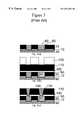
- FIGS. 1 a - 1 dshow the prior art process flow for the formation of a single damascene starting structure.
- FIGS. 2 a - 2 dare a process flow for the formation of a single damascene structure according to the invention.
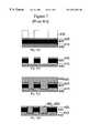
- FIGS. 3 a - 3 care a process flow of the prior art formation of a via-up single damascene structure.
- FIGS. 4 a - 4 care a process flow for the formation of a via-up dual damascene structure according to the invention.
- FIGS. 5 a - 5 care a process flow for the formation of a prior art line-up single and dual damascene structures.
- FIGS. 6 a - 6 care a process flow for the formation of a line-up dual damascene structure according to the invention.
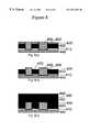
- FIGS. 7 a - 7 dare a process flow for the formation of a prior art hard mask layer over a low dielectric constant layer.
- FIGS. 8 a - 8 care a process flow for the removal of the hard mask layer according to the invention.
- a starting single damascene structureis fabricated by methods generally known in the art.
- the structureconsists of a conducting layer 60 and its associated liner layer 50 , which are embedded within an insulating layer 20 .
- the conducting metalis Cu
- the associated liner layer 50consists of a thin layer of Tantalum Nitride (TaN), followed by a thin layer of Tantalum (Ta), and then a Copper (Cu) seed layer.
- TaNTantalum Nitride
- TiTantalum
- CuCopper
- the details of forming the liner layer 50are disclosed in commonly owned co-pending application Ser. No. 08/497,065, now abandoned, and replaced by Ser. No. 08/896,925 and Ser. No. 09/370,003, the contents of which are hereby incorporated herein by reference.
- the method for fabricating this known starting structureis illustrated in FIGS. 1 ( a )-( d ), and includes the following steps:
- FIG. 1A more detailed description of the formation of the structure shown in FIG. 1 is provided in commonly owned U.S. Pat. No. 4,944,836, entitled “Chem-Mech Polishing Method For Producing Coplanar Metal/Insulator Films On A Substrate” and U.S. Pat. No. 4,789,648, entitled “Method For Producing Coplanar Multi-Level Metal/Insulator Films On A Substrate And For Forming Patterned Conductive Lines Simultaneously With Stud Vias,” the contents of which are incorporated herein by reference.
- a summary of the process flowproceeds as follows.
- An optional etch stop layer 10 and dielectric layer 20are deposited onto a substrate 40 .
- the resulting structureis patterned as necessary with a photoresist layer 30 , as shown in FIG. 1 ( a ).
- the photoresist patternis transferred into the dielectric layer 20 and optional etch stop layer 10 in a manner generally known in the art.
- the photoresist 30is then stripped in a conventional manner, as shown in FIG. 1 ( b ).
- a liner material 50 and conducting material 60are deposited onto the structure shown in FIG. 1 ( b ).
- the conducting layer 60 and liner layer 50are then planarized via a CMP process to form the desired pattern of conductor 60 in insulating layer 20 , shown in FIG. 1 ( d ).
- the dielectric 20 and etch stop 10 layersare then selectively removed.
- This removalis preferably accomplished using a plasma etching technique in a commercially available plasma etch tool, such as the High Density Plasma (HDP) Oxide Etcher sold by Applied Materials Corp. of Santa Clara, Calif.
- a plasma etching techniquesuch as the High Density Plasma (HDP) Oxide Etcher sold by Applied Materials Corp. of Santa Clara, Calif.
- HDPHigh Density Plasma
- SCCMstandard cubic centimeters per minute
- the reactor vessel(not shown) is configured such that the pressure within it is at 8 mTorr, with the roof at a temperature of 220° C., the walls at 215° C., the wafer pedestal at 5° C., the He backside cooling pressure at 15 Torr, and the applied electromagnetic energy divided between 1200 Watts on the plasma source inductive coil and 1000 watts on the wafer pedestal.
- the etch processproceeds to selectively remove the dielectric layer 20 and etch stop layer 10 , as shown in FIG. 2 ( b ).
- the conductor 60 and liner 50 layersare protected by the deposition of a passivating layer 70 .
- a self-aligned side wall spacer 80 of dielectric layer 20 and optional etch stop layer 10are also formed as a by-product of this process.
- the insulating materialis then removed until it is down to the bottom of the conducting layer 60 (see FIG. 2 ( b )).
- additional materialmay be removed from the substrate 40 such that the depth of removal is beneath the depth of the conductor 60 and liner 50 layers, as shown in FIG. 2 ( c ).
- the removed dielectricis then replaced by another dielectric layer 90 with properties different from removed dielectric layer 20 and optional etch stop 10 to yield the structure shown in FIG. 2 ( d ).
- the conducting layer 60 and its associated liner layer 50are left completely intact and are encased within a protective layer that consists of C and F bound in various chemical forms.
- a protective layerthat consists of C and F bound in various chemical forms.
- Other known processes to remove dielectricuse an organic dielectric, which can easily be removed with an O 2 ash. However, this process may oxidize a Cu conductor, and will not form a self-aligned sidewall spacer, which helps to provide structural integrity when the dielectric is removed.
- the passivating layer 70may be removed prior to deposition of dielectric layer 90 .
- the removalcan be accomplished in many different manners.
- One presently preferred techniqueconsists of removing the passivating layer 70 within the same reactor vessel used to do the plasma etching process. In this case, O 2 is applied at a rate of 300 SCCM, and the vessel configured such that it is at 15 mTorr pressure, with an applied power of 2500 W on the source coil, and 300 W on the wafer pedestal, with all other parameters remaining unchanged from the etch process.
- the etchingproceeds until the passivating layer 70 is removed. This process does not greatly oxidize a copper conductor due to the low temperature and bias power employed.
- feed gas mixturesconsisting of gases chosen from the following list (O 2 , N 2 , H 2 , NH 3 , N 2 H 2 , CF 4 , CO 2 , CO, CH 4 , C 2 H 2 , C 2 H 4 ) in an reactor such as used for the plasma etch process, or in another suitable reactor.
- the dielectric layer 20is removed to a depth concurrent with the bottom of the conductor layer 60 .
- the dielectric layer 20is removed to a depth non-concurrent with the bottom of the conductor 60 , particularly if that depth is deeper than the conductor depth.
- the resulting structuremay be filled with a new dielectric to replace the removed dielectric.
- the new dielectricis preferably chosen to have certain key properties that the removed dielectric did not have, such as a lower dielectric constant.
- This embodiment of the inventionbegins with a known structure consisting of two conducting layers built into a conventional dielectric material.
- FIGS. 3 and 4A process flow for this embodiment of the invention is shown in FIGS. 3 and 4.
- the starting structure shown in FIGS. 3 ( a )-( c )proceeds as described above in connection with FIG. 1 .
- an optional etch stop layer 100 and a via dielectric layer 110are deposited, and patterned with photoresist 120 as shown in FIG. 3 ( b ).
- the photoresist patternis transferred into the dielectric layer 110 and optional etch stop layer 100 in a manner generally known in the art.
- a liner layer 130 and conductor layer 140are then deposited as shown in FIG. 3 ( c ).
- the conductor 140 and liner 130 layersare planarized using CMP to form a desired conductor pattern in layer 110 , as shown in FIG. 3 ( c ).
- the dielectric layer 110 and optional dielectric layer 100 , and dielectric layer 20 and optional dielectric layer 10are selectively removed.
- Conductors 140 and 60 and liners 130 and 50are protected by the deposition of a passivating layer 150 (FIG. 4 ( b )).
- a self-aligned sidewall spacer 160 of dielectrics 110 and 20 and optional dielectrics 100 and 10is again formed by this process.
- the removal of dielectric 20may optionally proceed beneath the level of conductor 60 into substrate 40 , as described above, as shown in FIG. 4 ( c ).
- the removed dielectricsare preferably replaced by another dielectric 170 with properties different from removed dielectrics 110 and 20 and optional etch stops 10 and 100 .
- passivating layer 150may be removed prior to deposition of dielectric 170 .
- This embodiment of the inventionbegins with a known structure consisting of two conducting layers built into a conventional dielectric material, as shown in FIGS. 5 ( a )-( c ).
- One layer, the top layer,is a conducting layer consisting of lines of conductor, while the bottom layer consists of interconnections to vias formed beneath a conductor line layer.
- the process flowbegins in FIG. 5 and continues in FIG. 6 .
- the initial structureis formed by depositing an optional etch stop layer 210 , and via dielectric 220 onto the substrate 200 .
- a photoresist patternis transferred into dielectric 220 and optional etch stop 210 .
- a liner 260 and conductor 280are next deposited.
- the conductor 280 and liner 260are then planarized via CMP to form the desired conductor pattern in layer 220 shown in FIG. 5 ( a ).
- an optional etch stop layer 230 , and line dielectric 240are deposited onto the substrate 200 shown in FIG. 5 ( a ).
- a photoresist patternis transferred into the dielectric 240 and optional etch stop 230 .
- the liner layer 250 and conductor layer 270are then deposited.
- the conductor 270 and liner 250are again planarized via CMP to form a desired conductor pattern in layer 240 , as shown in FIG. 5 ( b ).
- Other known methodsmay be used to form the two levels simultaneously such that conductors 270 and 280 are the same conductor 290 , and liners 250 and 260 are the same liners 300 , as shown in FIG. 5 ( c ).
- the processcontinues as shown in FIG. 6 ( a ) to selectively remove dielectric 240 and optional dielectric 230 , and dielectric 220 and optional dielectric 210 .
- Conductor 290 and liner 300are protected by the deposition of a passivating layer 310 .
- a self-aligned sidewall spacer 320 of dielectrics 240 and 220 and optional dielectrics 230 and 210is again formed by this process.
- the removal of dielectric 210may optionally proceed beneath the level of conductor 290 into substrate 200 , as shown in FIG. 6 ( b ).
- the removed dielectricsare then replaced by another dielectric 330 with properties different from removed dielectrics 240 and 220 and optional etch stops 210 and 230 .
- passivating layer 310may be optionally removed.
- a further embodiment of the inventionuses the application of various films as processing aids to protect an underlying low dielectric constant material.
- the process of depositing and removing a hard mask layer dielectric having a higher dielectric constant than the underlying dielectric layeris illustrated in FIGS. 7 and 8. In the presently preferred embodiment of the process illustrated in FIGS.
- the dielectric layer depositedcan comprise any of the following materials: silicon dioxide, polyimide, organic siloxane polymer, poly-arlyene ether, carbon- or hydrogen-doped silicate glass or silsesquioxane glass, spin-on glass, fluorinated or non-fluorinated silicate glass, diamond like amorphous carbon, nano-porous silicate or organosilicate glass or silsesquioxane polymer, or any similar low dielectric constant material known in the art to be a useful dielectric material.
- the hard mask layercomprises any of the dielectrics known in the art and listed above in the Background section.
- an optional etch stop layer 410is first deposited onto a semiconductor substrate 440 in a manner generally known in the art.
- the etch stop layer 410is followed the deposition of a dielectric layer 420 , and then a hard mask layer 425 deposited on top of the dielectric layer 420 .
- the resulting structureis patterned with photoresist 430 , as shown in FIG. 7 ( a ).
- the pattern from photoresist 430is then transferred into the hard mask layer 425 , the dielectric layer 420 and the optional etch stop layer 410 , and the photoresist layer 430 is then stripped off, as shown in FIG. 7 ( b ).
- Layers of liner material 450 and conducting material 460are then deposited, as shown in FIG. 7 ( c ).
- the conducting layer 460 and liner layer 450are planarized, preferably through a CMP process, to form the desired pattern of conductor in the layers of hard mask 425 , insulating layer 420 , and optional etch stop 410 .
- the resulting known structureis shown in FIG. 7 ( d ).
- FIGS. 7 and 8those skilled in the art will appreciate that the hard mask layer 425 can be used and applied with a dual damascene structure as well.
- the hard mask layer 425is then selectively removed without damaging the conductor layer 460 , liner layer 450 , or dielectric layer 420 , as shown in FIG. 8 ( b ).
- the passivating layer 470is simultaneously deposited while the hard mask layer 425 is removed.
- the preferred process for removing the hard mask layer 420 and simultaneously depositing the passivating layer 470is the same as disclosed above.
- the passivating layer 470is then removed without oxidizing conductor layer 460 , liner layer 450 , or dielectric layer 420 .
- the preferred method to remove the passivating layeris done in a capacitively-coupled reactive ion etch system such as one sold by Applied Materials of Santa Clara, Calif. under the name MxP using a mixture of 40 SCCM NH 3 and 40 SCCM H 2 at a pressure of 100 mT and a power of 100 Watts with a cathode temperature of 60° C.
- a second low dielectric constant dielectric layer 480can be deposited, as shown in FIG. 8 ( c ).
Landscapes
- Engineering & Computer Science (AREA)
- Physics & Mathematics (AREA)
- Condensed Matter Physics & Semiconductors (AREA)
- General Physics & Mathematics (AREA)
- Manufacturing & Machinery (AREA)
- Computer Hardware Design (AREA)
- Microelectronics & Electronic Packaging (AREA)
- Power Engineering (AREA)
- Internal Circuitry In Semiconductor Integrated Circuit Devices (AREA)
Abstract
Description
This invention relates to semiconductor integrated circuit processing, and more particularly to a method for fabricating interconnect structures in quartz or related dielectric films and then selectively removing the dielectric without damaging the conducting layers.
Fabrication of interconnect structures for semiconductors is conventionally accomplished using silicon dioxide (SiO2) as the dielectric and Al or Cu as the metallic conducting film. Current processes are optimized for these materials. However, new dielectrics are becoming available with more advantageous properties such as a reduced dielectric constant which can increase the speed of integrated circuits. The processing of these new dielectrics, however, has not yet been optimized.
Various films (“processing aids”) are used in the processing of low dielectric constant (k) materials, particularly to protect the low-k material from erosion during a chemical-mechanical polish (CMP) process. These “processing aid” films have a higher dielectric constant than the low-k films, and if left in the final structure, would increase the final effective dielectric constant, thus degrading the effect of the low dielectric constant insulator. Removing these films after they have served the integration purpose is thus desirable.
Reactive ion etching is one known method of removing dielectric films, but results in either the sputtering of exposed copper, removal of exposed liners, or contamination of the dielectric surface by redeposition of copper sputtered during the etch process. Additionally, damage or modification of the underlying protected low-k dielectric may occur due to exposure to the plasma process. With current copper liner metallurgy, etch of “processing aid” films (such as silicon dioxide or silicon nitride) can also etch the liner materials since these liners are etched in the same chemistries as the “processing aid” films.
Plasma etching is a commonly used technique for semiconductor manufacturing. Plasma etching consists of the application of an electromagnetic energy field to a suitable reactor vessel containing desired feed gas species and a substrate that is to be etched (typically a Si wafer, GaAs wafer or other such substrate). The choice of feed gas species and their rate of application, the amount of electromagnetic energy applied, and the configuration of the reactor vessel, all work together to determine the specific etch characteristics for that particular process. These characteristics include how quickly and uniformly different materials etch, and how the microstructure (profile/shape) of the materials evolves in time. The etch processes work by a number of simultaneous etching mechanisms, such as physical sputtering, spontaneous chemical etching, and chemical assisted sputtering.
It is known that certain feed gases or mixtures of feed gases are better suited to etch certain materials than other feed gases or mixtures. Thus, one knowledgeable in the art may choose gases containing certain elemental species because they are better suited for a particular problem. Still, the specific choice of feed gases to do a specific job is not automatic. Instead, the feed gas or mixture and rate of application are carefully chosen to balance a number of competing factors in the etch process evolution.
One desirable behavior in etch processes is a selective etch. Plasma etching possesses the ability to remove one or more materials that are desired to be removed, while not removing one or materials that are desired to remain in place. Some materials combinations easily confer the ability for one material to be removed selectively to others. For example, it is known that organic polymers may be removed selectively to silicon dioxide using a plasma containing oxygen feed gas. Other materials combinations present more of a problem to etch selectively. This often arises because the feed gas or mixture that etches one material will also etch other materials.
During the construction of integrated circuit devices, it is often necessary to construct structures where a conducting material or conducting materials are placed within an insulating layer in a three dimensional fashion. Further, this (these) conduction material(s) are often interconnected. For certain reasons, such as performance and ease of construction, it is sometimes desirable to build structures in one insulating material, but then replace it with another insulating material. In this case, it is desirable to be able to selectively remove the insulating material without damaging, degrading, or changing the conducting material(s).
In particular, a structure may be built in which the insulating material is chosen from materials such as silicon dioxide, silicon nitride, fluorinated silicon glass, undoped silicon glass, phosphorus silicon glass, boron-phosphorous silicon glass, and associated insulators in stoichiometric or non-stoichiometric forms. This structure may further be processed by known methods so that the insulating layer contains a conducting layer that consists of a conducting metal (e.g., Cu, Al, W, Ag) or conducting semiconductor (e.g., Si, Ge, C with appropriate impurities) and its associated “liner” layers (which are often refractory metals (Ta, Ti, W), refraction metal nitrides (TaN, TiN, WN), refractory metal alloys (TaSiN), or a combination of these materials). To replace the insulating material with another material, it is desirable to have an etch process that can remove the insulator without removing, damaging, or degrading the conducting layer or its associated “liner” material(s). If incorrect conditions are used, then the conducting layer(s) and its' (their) associated liner layer(s) can be eroded, leaving a small pointed region of conductor.
In view of the above, the protection of exposed conductor and liner surfaces is accomplished by deposition of a plasma generated polymer film during a dielectric etch process. A plasma process chemistry is chosen to allow etching of the removable dielectric film while depositing a protective film on the exposed metal surfaces. This protective film will prevent subsequent etching or sputtering of the exposed conductor and liner materials. The polymer film on the metal surfaces can be removed in a subsequent process step by a technique that will not damage the exposed conductor surface, such as a down stream plasma asher, chemical dry etcher, low-bias reactive ion etcher, or in a suitable wet process.
As the sacrificial dielectric film is etched to endpoint, a protective film deposited on the now-exposed underlying low-k film (if present) will prevent plasma modification of this underlying dielectric. This is particularly critical to low-k systems such as Hydrogen Silsesquioxane (HSSQ) or Methylsilsesquioxane (MSSQ), which can be substantially modified to give a higher dielectric constant film. The process that removes the protective polymer from the conductor or liner surfaces will also remove it from the low-k film surface.
These and other features and advantages of the invention will become apparent upon a review of the following detailed description of the presently preferred embodiments of the invention, when viewed in conjunction with the appended drawings.
FIGS. 1a-1dshow the prior art process flow for the formation of a single damascene starting structure.
FIGS. 2a-2dare a process flow for the formation of a single damascene structure according to the invention.
FIGS. 3a-3care a process flow of the prior art formation of a via-up single damascene structure.
FIGS. 4a-4care a process flow for the formation of a via-up dual damascene structure according to the invention.
FIGS. 5a-5care a process flow for the formation of a prior art line-up single and dual damascene structures.
FIGS. 6a-6care a process flow for the formation of a line-up dual damascene structure according to the invention.
FIGS. 7a-7dare a process flow for the formation of a prior art hard mask layer over a low dielectric constant layer.
FIGS. 8a-8care a process flow for the removal of the hard mask layer according to the invention.
To accomplish the removal of the dielectric layer without degradation of the conducting layer, all of the different etch mechanisms (physical sputtering, spontaneous chemical etching, and chemical assisted sputtering) should be controlled such that the dielectric is removed while the conducting layer is not. The material(s) of the conducting layer are thus “passivated” by the plasma to prevent its (their) loss. One presently preferred method for accomplishing this is to passivate the conducting layer and its associated “liner” layers by selectively covering these layers with a material from the plasma, while selectively not covering the insulating material with material from the plasma. This may be accomplished by a judicious choice of feed gases and their rate of application, the amount of electromagnetic energy applied, and the configuration of the reactor vessel. As described in greater detail below, several embodiments of this method of the invention are contemplated. Line-only single damascene, via-up dual damascene, line-up dual damascene, and high dielectric constant layer embodiments are provided.
Line-Only Single Damascene
Referring first to FIGS. 1a-1d, a starting single damascene structure is fabricated by methods generally known in the art. The structure consists of aconducting layer 60 and its associatedliner layer 50, which are embedded within an insulatinglayer 20. In one preferred embodiment of the invention, the conducting metal is Cu, and the associatedliner layer 50 consists of a thin layer of Tantalum Nitride (TaN), followed by a thin layer of Tantalum (Ta), and then a Copper (Cu) seed layer. The details of forming theliner layer 50 are disclosed in commonly owned co-pending application Ser. No. 08/497,065, now abandoned, and replaced by Ser. No. 08/896,925 and Ser. No. 09/370,003, the contents of which are hereby incorporated herein by reference. The method for fabricating this known starting structure is illustrated in FIGS.1(a)-(d), and includes the following steps:
1. Dielectric deposition & photolithographic definition of a pattern (FIG.1(a)).
2. Plasma etching of the pattern into the dielectric (FIG.1(b)).
3. Liner deposition & conducting layer deposition (FIG.1(c)).
4. Metal & liner planarization by chemical mechanical planarization (FIG.1(d)).
A more detailed description of the formation of the structure shown in FIG. 1 is provided in commonly owned U.S. Pat. No. 4,944,836, entitled “Chem-Mech Polishing Method For Producing Coplanar Metal/Insulator Films On A Substrate” and U.S. Pat. No. 4,789,648, entitled “Method For Producing Coplanar Multi-Level Metal/Insulator Films On A Substrate And For Forming Patterned Conductive Lines Simultaneously With Stud Vias,” the contents of which are incorporated herein by reference.
A summary of the process flow proceeds as follows. An optionaletch stop layer 10 anddielectric layer 20 are deposited onto asubstrate 40. The resulting structure is patterned as necessary with aphotoresist layer 30, as shown in FIG.1(a). The photoresist pattern is transferred into thedielectric layer 20 and optionaletch stop layer 10 in a manner generally known in the art. Thephotoresist 30 is then stripped in a conventional manner, as shown in FIG.1(b). In FIG.1(c), aliner material 50 and conductingmaterial 60 are deposited onto the structure shown in FIG.1(b). The conductinglayer 60 andliner layer 50 are then planarized via a CMP process to form the desired pattern ofconductor 60 in insulatinglayer 20, shown in FIG.1(d).
Continuing with the structure shown in FIGS.1(d) and2(a), the dielectric20 and etch stop10 layers are then selectively removed. This removal is preferably accomplished using a plasma etching technique in a commercially available plasma etch tool, such as the High Density Plasma (HDP) Oxide Etcher sold by Applied Materials Corp. of Santa Clara, Calif. To do this, a mixture of feed gases consisting of Ar, C2F6, and cyclo-C4F8are employed, at an application rate of 150, 10, and 10 standard cubic centimeters per minute (SCCM), respectively. The reactor vessel (not shown) is configured such that the pressure within it is at 8 mTorr, with the roof at a temperature of 220° C., the walls at 215° C., the wafer pedestal at 5° C., the He backside cooling pressure at 15 Torr, and the applied electromagnetic energy divided between 1200 Watts on the plasma source inductive coil and 1000 watts on the wafer pedestal.
The etch process proceeds to selectively remove thedielectric layer 20 andetch stop layer 10, as shown in FIG.2(b). Theconductor 60 andliner 50 layers are protected by the deposition of apassivating layer 70. A self-alignedside wall spacer 80 ofdielectric layer 20 and optionaletch stop layer 10 are also formed as a by-product of this process. The insulating material is then removed until it is down to the bottom of the conducting layer60 (see FIG.2(b)). Alternatively, additional material may be removed from thesubstrate 40 such that the depth of removal is beneath the depth of theconductor 60 andliner 50 layers, as shown in FIG.2(c). The removed dielectric is then replaced by another dielectric layer90 with properties different from removeddielectric layer 20 and optional etch stop10 to yield the structure shown in FIG.2(d).
The conductinglayer 60 and its associatedliner layer 50 are left completely intact and are encased within a protective layer that consists of C and F bound in various chemical forms. Other known processes to remove dielectric use an organic dielectric, which can easily be removed with an O2ash. However, this process may oxidize a Cu conductor, and will not form a self-aligned sidewall spacer, which helps to provide structural integrity when the dielectric is removed.
In an alternate embodiment of the invention, prior to deposition of dielectric layer90, thepassivating layer 70 may be removed. The removal can be accomplished in many different manners. One presently preferred technique consists of removing thepassivating layer 70 within the same reactor vessel used to do the plasma etching process. In this case, O2is applied at a rate of 300 SCCM, and the vessel configured such that it is at 15 mTorr pressure, with an applied power of 2500 W on the source coil, and 300 W on the wafer pedestal, with all other parameters remaining unchanged from the etch process. The etching proceeds until thepassivating layer 70 is removed. This process does not greatly oxidize a copper conductor due to the low temperature and bias power employed. Other preferred techniques consist of removing thepassivating layer 70 using feed gas mixtures consisting of gases chosen from the following list (O2, N2, H2, NH3, N2H2, CF4, CO2, CO, CH4, C2H2, C2H4) in an reactor such as used for the plasma etch process, or in another suitable reactor.
In one embodiment, thedielectric layer 20 is removed to a depth concurrent with the bottom of theconductor layer 60. In an alternate embodiment, thedielectric layer 20 is removed to a depth non-concurrent with the bottom of theconductor 60, particularly if that depth is deeper than the conductor depth. At this point, the resulting structure may be filled with a new dielectric to replace the removed dielectric. The new dielectric is preferably chosen to have certain key properties that the removed dielectric did not have, such as a lower dielectric constant.
Via-Up Dual Damascene
This embodiment of the invention begins with a known structure consisting of two conducting layers built into a conventional dielectric material. One layer, the bottom layer, is a conducting layer consisting of lines of conductor, while the top layer consists of interconnections (“vias”) to another layer.
A process flow for this embodiment of the invention is shown in FIGS. 3 and 4. The starting structure shown in FIGS.3(a)-(c) proceeds as described above in connection with FIG.1. After creating the structure shown in FIG.3(a), an optionaletch stop layer 100 and a viadielectric layer 110 are deposited, and patterned withphotoresist 120 as shown in FIG.3(b). The photoresist pattern is transferred into thedielectric layer 110 and optionaletch stop layer 100 in a manner generally known in the art. Aliner layer 130 andconductor layer 140 are then deposited as shown in FIG.3(c). Theconductor 140 andliner 130 layers are planarized using CMP to form a desired conductor pattern inlayer 110, as shown in FIG.3(c).
Referring now to FIG.4(a), thedielectric layer 110 andoptional dielectric layer 100, anddielectric layer 20 andoptional dielectric layer 10 are selectively removed.Conductors liners sidewall spacer 160 ofdielectrics optional dielectrics conductor 60 intosubstrate 40, as described above, as shown in FIG.4(c). The removed dielectrics are preferably replaced by another dielectric170 with properties different from removeddielectrics dielectric 170,passivating layer 150 may be removed.
Line-Up Dual Damascene
This embodiment of the invention begins with a known structure consisting of two conducting layers built into a conventional dielectric material, as shown in FIGS.5(a)-(c). One layer, the top layer, is a conducting layer consisting of lines of conductor, while the bottom layer consists of interconnections to vias formed beneath a conductor line layer.
The process flow begins in FIG.5 and continues in FIG.6. The initial structure is formed by depositing an optionaletch stop layer 210, and viadielectric 220 onto thesubstrate 200. A photoresist pattern is transferred intodielectric 220 andoptional etch stop 210. A liner260 and conductor280 are next deposited. The conductor280 and liner260 are then planarized via CMP to form the desired conductor pattern inlayer 220 shown in FIG.5(a).
Referring to FIG.5(b), an optionaletch stop layer 230, and line dielectric240 are deposited onto thesubstrate 200 shown in FIG.5(a). A photoresist pattern is transferred into the dielectric240 andoptional etch stop 230. Theliner layer 250 andconductor layer 270 are then deposited. Theconductor 270 andliner 250 are again planarized via CMP to form a desired conductor pattern inlayer 240, as shown in FIG.5(b). Other known methods may be used to form the two levels simultaneously such thatconductors 270 and280 are thesame conductor 290, andliners 250 and260 are thesame liners 300, as shown in FIG.5(c).
The process continues as shown in FIG.6(a) to selectively remove dielectric240 andoptional dielectric 230, and dielectric220 andoptional dielectric 210.Conductor 290 andliner 300 are protected by the deposition of apassivating layer 310. A self-alignedsidewall spacer 320 ofdielectrics optional dielectrics dielectric 210 may optionally proceed beneath the level ofconductor 290 intosubstrate 200, as shown in FIG.6(b). The removed dielectrics are then replaced by another dielectric330 with properties different from removeddielectrics dielectric 330,passivating layer 310 may be optionally removed.
High And Low Dielectric Constant Dielectrics
A further embodiment of the invention uses the application of various films as processing aids to protect an underlying low dielectric constant material. The process of depositing and removing a hard mask layer dielectric having a higher dielectric constant than the underlying dielectric layer is illustrated in FIGS. 7 and 8. In the presently preferred embodiment of the process illustrated in FIGS. 7 and 8, the dielectric layer deposited can comprise any of the following materials: silicon dioxide, polyimide, organic siloxane polymer, poly-arlyene ether, carbon- or hydrogen-doped silicate glass or silsesquioxane glass, spin-on glass, fluorinated or non-fluorinated silicate glass, diamond like amorphous carbon, nano-porous silicate or organosilicate glass or silsesquioxane polymer, or any similar low dielectric constant material known in the art to be a useful dielectric material. Preferably, the hard mask layer comprises any of the dielectrics known in the art and listed above in the Background section.
Referring to FIG. 7, an optionaletch stop layer 410 is first deposited onto asemiconductor substrate 440 in a manner generally known in the art. Theetch stop layer 410 is followed the deposition of adielectric layer 420, and then ahard mask layer 425 deposited on top of thedielectric layer 420. The resulting structure is patterned withphotoresist 430, as shown in FIG.7(a). The pattern fromphotoresist 430 is then transferred into thehard mask layer 425, thedielectric layer 420 and the optionaletch stop layer 410, and thephotoresist layer 430 is then stripped off, as shown in FIG.7(b).
Layers ofliner material 450 and conductingmaterial 460 are then deposited, as shown in FIG.7(c). Theconducting layer 460 andliner layer 450 are planarized, preferably through a CMP process, to form the desired pattern of conductor in the layers ofhard mask 425, insulatinglayer 420, andoptional etch stop 410. The resulting known structure is shown in FIG.7(d). Although a single damascene structure is shown in FIGS. 7 and 8, those skilled in the art will appreciate that thehard mask layer 425 can be used and applied with a dual damascene structure as well.
Beginning with the known structure illustrated in FIGS.7(d) and8(a), thehard mask layer 425 is then selectively removed without damaging theconductor layer 460,liner layer 450, ordielectric layer 420, as shown in FIG.8(b). Thepassivating layer 470 is simultaneously deposited while thehard mask layer 425 is removed. The preferred process for removing thehard mask layer 420 and simultaneously depositing thepassivating layer 470 is the same as disclosed above. Thepassivating layer 470 is then removed without oxidizingconductor layer 460,liner layer 450, ordielectric layer 420. In this case, the preferred method to remove the passivating layer is done in a capacitively-coupled reactive ion etch system such as one sold by Applied Materials of Santa Clara, Calif. under the name MxP using a mixture of 40 SCCM NH3and 40 SCCM H2at a pressure of 100 mT and a power of 100 Watts with a cathode temperature of 60° C. Once the passivating layer has been removed, a second low dielectricconstant dielectric layer 480 can be deposited, as shown in FIG.8(c).
It is to be understood that a wide range of changes and modifications to the embodiments described above will be apparent to those skilled in the art and are contemplated. It is therefore intended that the foregoing detailed description be regarded as illustrative, rather than limiting, and that it be understood that it is the following claims, including all equivalents, that are intended to define the spirit and scope of the invention.
Claims (29)
1. A method for etching a dielectric layer in a semiconductor integrated circuit fabrication process without damaging an underlying layer of metalization, comprising the steps of:
patterning a dielectric layer deposited on top of a substrate;
depositing a conducting layer of metalization within the patterned dielectric layer;
planarizing the layer of metalization via a chemical mechanical polishing process; and
depositing a passivating layer on top of the layer of metalization after the metalization has been planarized and simultaneously etching the dielectric layer without damaging the conducting layer of metalization.
2. The method defined inclaim 1 , further comprising the step of depositing an etch stop layer prior to depositing the dielectric layer.
3. The method defined inclaim 2 , wherein the step of etching the dielectric layer proceeds to a stop point defined by the etch stop layer.
4. The method defined inclaim 1 , wherein the step of etching the dielectric layer proceeds to a level of the underlying layer of metalization.
5. The method defined inclaim 1 , wherein the step of etching the dielectric layer proceeds to a level below the underlying layer of metalization.
6. The method defined inclaim 1 , further comprising the step of patterning the dielectric layer through the use of a photoresist pattern.
7. The method defined inclaim 1 , wherein the step of etching the dielectric layer comprises the step of plasma etching.
8. The method defined inclaim 7 , wherein the plasma etch consists of a mixture of feed gases.
9. The method defined inclaim 8 , wherein the mixture of feed gases comprises Ar, C2F6, and cyclo-C4F8.
10. The method defined inclaim 1 , further comprising the step of forming a self-aligned side wall spacer formed from the dielectric layer.
11. The method defined inclaim 1 , wherein the etched dielectric is replaced by another dielectric layer having different properties.
12. The method defined inclaim 11 , wherein the different properties comprise having a lower dielectric constant.
13. The method defined inclaim 1 , wherein the conductor layer of metalization is encased with carbon and fluorine bound in various chemical forms.
14. The method defined inclaim 1 , further comprising the step of depositing a liner layer before deposition of the conducting layer of metalization.
15. The method defined inclaim 1 , wherein the dielectric layer comprises silicon dioxide.
16. The method defined inclaim 14 , wherein the liner layer comprises tantalum.
17. The method defined inclaim 14 , wherein the liner layer comprises tantalum nitride.
18. The method defined inclaim 14 , wherein the liner layer comprises tantalum and tantalum nitride.
19. The method defined inclaim 1 , wherein the metalization layer comprises copper.
20. The method defined inclaim 1 , further comprising the step of removing the passivating layer without damaging the metalization and liner layers.
21. A method for etching a dielectric layer in a semiconductor integrated circuit fabrication process without damaging an underlying layer of metalization, comprising the steps of:
depositing a first dielectric on top of a semiconductor substrate, the first dielectric having a low dielectric constant;
depositing a second dielectric on top of the first dielectric, the second dielectric having a dielectric constant higher than the first dielectric;
patterning the first and second dielectrics;
depositing a conducting layer of metalization within the patterned first and second dielectrics;
planarizing the layer of metalization via a chemical mechanical polishing process; and
depositing a passivating layer on top of the layer of metalization after the metalization has been planarized and simultaneously etching the second dielectric without damaging the conducting layer of metalization.
22. The method defined inclaim 21 , further comprising the step of depositing an etch stop layer prior to depositing the first dielectric.
23. The method defined inclaim 21 , wherein the etched second dielectric is replaced by a third dielectric having a lower dielectric constant.
24. The method defined inclaim 21 , further comprising the step of depositing a liner layer before deposition of the conducting layer of metalization.
25. The method defined inclaim 24 , wherein the liner layer comprises tantalum.
26. The method defined inclaim 24 , wherein the liner layer comprises tantalum nitride.
27. The method defined inclaim 24 , wherein the liner layer comprises tantalum and tantalum nitride.
28. The method defined inclaim 21 , wherein the metalization layer comprises copper.
29. The method defined inclaim 21 , further comprising the step of removing the passivating layer without damaging the metalization and liner layer.
Priority Applications (2)
| Application Number | Priority Date | Filing Date | Title |
|---|---|---|---|
| US09/432,683US6551924B1 (en) | 1999-11-02 | 1999-11-02 | Post metalization chem-mech polishing dielectric etch |
| KR10-2000-0064520AKR100371591B1 (en) | 1999-11-02 | 2000-11-01 | Post metalization chem-mech polishing dielectric etch |
Applications Claiming Priority (1)
| Application Number | Priority Date | Filing Date | Title |
|---|---|---|---|
| US09/432,683US6551924B1 (en) | 1999-11-02 | 1999-11-02 | Post metalization chem-mech polishing dielectric etch |
Publications (1)
| Publication Number | Publication Date |
|---|---|
| US6551924B1true US6551924B1 (en) | 2003-04-22 |
Family
ID=23717179
Family Applications (1)
| Application Number | Title | Priority Date | Filing Date |
|---|---|---|---|
| US09/432,683Expired - Fee RelatedUS6551924B1 (en) | 1999-11-02 | 1999-11-02 | Post metalization chem-mech polishing dielectric etch |
Country Status (2)
| Country | Link |
|---|---|
| US (1) | US6551924B1 (en) |
| KR (1) | KR100371591B1 (en) |
Cited By (164)
| Publication number | Priority date | Publication date | Assignee | Title |
|---|---|---|---|---|
| US20030017694A1 (en)* | 2001-07-23 | 2003-01-23 | Applied Materials, Inc. | Selective etching of organosilicate films over silicon oxide stop etch layers |
| US20060051966A1 (en)* | 2004-02-26 | 2006-03-09 | Applied Materials, Inc. | In-situ chamber clean process to remove by-product deposits from chemical vapor etch chamber |
| US20060216924A1 (en)* | 2005-03-28 | 2006-09-28 | Zhen-Cheng Wu | BEOL integration scheme for etching damage free ELK |
| US20070032058A1 (en)* | 2005-08-03 | 2007-02-08 | Shu-Jen Sung | Method of fabricating interconnect |
| US20070141832A1 (en)* | 2005-12-08 | 2007-06-21 | Micron Technology, Inc. | Integrated circuit insulators and related methods |
| US20070202640A1 (en)* | 2006-02-28 | 2007-08-30 | Applied Materials, Inc. | Low-k spacer integration into CMOS transistors |
| US20070296083A1 (en)* | 2006-06-21 | 2007-12-27 | Micron Technology, Inc. | Low dielectric constant integrated circuit insulators and methods |
| US20080157382A1 (en)* | 2006-12-28 | 2008-07-03 | Chinthakindi Anil K | Direct termination of a wiring metal in a semiconductor device |
| US20080305639A1 (en)* | 2007-06-07 | 2008-12-11 | Taiwan Semiconductor Manufacturing Co., Ltd. | Dual damascene process |
| US20090095621A1 (en)* | 2004-02-26 | 2009-04-16 | Chien-Teh Kao | Support assembly |
| US20090181537A1 (en)* | 2007-04-30 | 2009-07-16 | Advanced Micro Devices, Inc. | Semiconductor structure comprising an electrical connection and method of forming the same |
| US20110049727A1 (en)* | 2009-08-31 | 2011-03-03 | Oliver Aubel | Recessed interlayer dielectric in a metallization structure of a semiconductor device |
| US8679983B2 (en) | 2011-09-01 | 2014-03-25 | Applied Materials, Inc. | Selective suppression of dry-etch rate of materials containing both silicon and nitrogen |
| US8679982B2 (en) | 2011-08-26 | 2014-03-25 | Applied Materials, Inc. | Selective suppression of dry-etch rate of materials containing both silicon and oxygen |
| US8765546B1 (en) | 2013-06-24 | 2014-07-01 | United Microelectronics Corp. | Method for fabricating fin-shaped field-effect transistor |
| US8765574B2 (en) | 2012-11-09 | 2014-07-01 | Applied Materials, Inc. | Dry etch process |
| US8771539B2 (en) | 2011-02-22 | 2014-07-08 | Applied Materials, Inc. | Remotely-excited fluorine and water vapor etch |
| US8801952B1 (en) | 2013-03-07 | 2014-08-12 | Applied Materials, Inc. | Conformal oxide dry etch |
| US8808563B2 (en) | 2011-10-07 | 2014-08-19 | Applied Materials, Inc. | Selective etch of silicon by way of metastable hydrogen termination |
| US8895449B1 (en) | 2013-05-16 | 2014-11-25 | Applied Materials, Inc. | Delicate dry clean |
| US8921234B2 (en) | 2012-12-21 | 2014-12-30 | Applied Materials, Inc. | Selective titanium nitride etching |
| US8927390B2 (en) | 2011-09-26 | 2015-01-06 | Applied Materials, Inc. | Intrench profile |
| US8951429B1 (en) | 2013-10-29 | 2015-02-10 | Applied Materials, Inc. | Tungsten oxide processing |
| US8956980B1 (en) | 2013-09-16 | 2015-02-17 | Applied Materials, Inc. | Selective etch of silicon nitride |
| US8969212B2 (en) | 2012-11-20 | 2015-03-03 | Applied Materials, Inc. | Dry-etch selectivity |
| US8975152B2 (en) | 2011-11-08 | 2015-03-10 | Applied Materials, Inc. | Methods of reducing substrate dislocation during gapfill processing |
| US8980763B2 (en) | 2012-11-30 | 2015-03-17 | Applied Materials, Inc. | Dry-etch for selective tungsten removal |
| US8999856B2 (en) | 2011-03-14 | 2015-04-07 | Applied Materials, Inc. | Methods for etch of sin films |
| US9023732B2 (en) | 2013-03-15 | 2015-05-05 | Applied Materials, Inc. | Processing systems and methods for halide scavenging |
| US9023734B2 (en) | 2012-09-18 | 2015-05-05 | Applied Materials, Inc. | Radical-component oxide etch |
| US9034770B2 (en) | 2012-09-17 | 2015-05-19 | Applied Materials, Inc. | Differential silicon oxide etch |
| US9040422B2 (en) | 2013-03-05 | 2015-05-26 | Applied Materials, Inc. | Selective titanium nitride removal |
| US9064816B2 (en) | 2012-11-30 | 2015-06-23 | Applied Materials, Inc. | Dry-etch for selective oxidation removal |
| US9064815B2 (en) | 2011-03-14 | 2015-06-23 | Applied Materials, Inc. | Methods for etch of metal and metal-oxide films |
| US9111877B2 (en) | 2012-12-18 | 2015-08-18 | Applied Materials, Inc. | Non-local plasma oxide etch |
| US9117855B2 (en) | 2013-12-04 | 2015-08-25 | Applied Materials, Inc. | Polarity control for remote plasma |
| US9114438B2 (en) | 2013-05-21 | 2015-08-25 | Applied Materials, Inc. | Copper residue chamber clean |
| US9132436B2 (en) | 2012-09-21 | 2015-09-15 | Applied Materials, Inc. | Chemical control features in wafer process equipment |
| US9136273B1 (en) | 2014-03-21 | 2015-09-15 | Applied Materials, Inc. | Flash gate air gap |
| US9159606B1 (en) | 2014-07-31 | 2015-10-13 | Applied Materials, Inc. | Metal air gap |
| US9165786B1 (en) | 2014-08-05 | 2015-10-20 | Applied Materials, Inc. | Integrated oxide and nitride recess for better channel contact in 3D architectures |
| US9190293B2 (en) | 2013-12-18 | 2015-11-17 | Applied Materials, Inc. | Even tungsten etch for high aspect ratio trenches |
| US9236266B2 (en) | 2011-08-01 | 2016-01-12 | Applied Materials, Inc. | Dry-etch for silicon-and-carbon-containing films |
| US9236265B2 (en) | 2013-11-04 | 2016-01-12 | Applied Materials, Inc. | Silicon germanium processing |
| US9245762B2 (en) | 2013-12-02 | 2016-01-26 | Applied Materials, Inc. | Procedure for etch rate consistency |
| US9263278B2 (en) | 2013-12-17 | 2016-02-16 | Applied Materials, Inc. | Dopant etch selectivity control |
| US9269590B2 (en) | 2014-04-07 | 2016-02-23 | Applied Materials, Inc. | Spacer formation |
| US9287095B2 (en) | 2013-12-17 | 2016-03-15 | Applied Materials, Inc. | Semiconductor system assemblies and methods of operation |
| US9287134B2 (en) | 2014-01-17 | 2016-03-15 | Applied Materials, Inc. | Titanium oxide etch |
| US9293568B2 (en) | 2014-01-27 | 2016-03-22 | Applied Materials, Inc. | Method of fin patterning |
| US9299582B2 (en) | 2013-11-12 | 2016-03-29 | Applied Materials, Inc. | Selective etch for metal-containing materials |
| US9299583B1 (en) | 2014-12-05 | 2016-03-29 | Applied Materials, Inc. | Aluminum oxide selective etch |
| US9299575B2 (en) | 2014-03-17 | 2016-03-29 | Applied Materials, Inc. | Gas-phase tungsten etch |
| US9299538B2 (en) | 2014-03-20 | 2016-03-29 | Applied Materials, Inc. | Radial waveguide systems and methods for post-match control of microwaves |
| US9299537B2 (en) | 2014-03-20 | 2016-03-29 | Applied Materials, Inc. | Radial waveguide systems and methods for post-match control of microwaves |
| US9309598B2 (en) | 2014-05-28 | 2016-04-12 | Applied Materials, Inc. | Oxide and metal removal |
| US9324576B2 (en) | 2010-05-27 | 2016-04-26 | Applied Materials, Inc. | Selective etch for silicon films |
| US9343272B1 (en) | 2015-01-08 | 2016-05-17 | Applied Materials, Inc. | Self-aligned process |
| US9349605B1 (en) | 2015-08-07 | 2016-05-24 | Applied Materials, Inc. | Oxide etch selectivity systems and methods |
| US9355862B2 (en) | 2014-09-24 | 2016-05-31 | Applied Materials, Inc. | Fluorine-based hardmask removal |
| US9355856B2 (en) | 2014-09-12 | 2016-05-31 | Applied Materials, Inc. | V trench dry etch |
| US9362130B2 (en) | 2013-03-01 | 2016-06-07 | Applied Materials, Inc. | Enhanced etching processes using remote plasma sources |
| US9368364B2 (en) | 2014-09-24 | 2016-06-14 | Applied Materials, Inc. | Silicon etch process with tunable selectivity to SiO2 and other materials |
| US9373517B2 (en) | 2012-08-02 | 2016-06-21 | Applied Materials, Inc. | Semiconductor processing with DC assisted RF power for improved control |
| US9373522B1 (en) | 2015-01-22 | 2016-06-21 | Applied Mateials, Inc. | Titanium nitride removal |
| US9378969B2 (en) | 2014-06-19 | 2016-06-28 | Applied Materials, Inc. | Low temperature gas-phase carbon removal |
| US9378978B2 (en) | 2014-07-31 | 2016-06-28 | Applied Materials, Inc. | Integrated oxide recess and floating gate fin trimming |
| US9385028B2 (en) | 2014-02-03 | 2016-07-05 | Applied Materials, Inc. | Air gap process |
| US9390937B2 (en) | 2012-09-20 | 2016-07-12 | Applied Materials, Inc. | Silicon-carbon-nitride selective etch |
| US9396989B2 (en) | 2014-01-27 | 2016-07-19 | Applied Materials, Inc. | Air gaps between copper lines |
| US9406523B2 (en) | 2014-06-19 | 2016-08-02 | Applied Materials, Inc. | Highly selective doped oxide removal method |
| US9425058B2 (en) | 2014-07-24 | 2016-08-23 | Applied Materials, Inc. | Simplified litho-etch-litho-etch process |
| US9449846B2 (en) | 2015-01-28 | 2016-09-20 | Applied Materials, Inc. | Vertical gate separation |
| US9478432B2 (en) | 2014-09-25 | 2016-10-25 | Applied Materials, Inc. | Silicon oxide selective removal |
| US9496167B2 (en) | 2014-07-31 | 2016-11-15 | Applied Materials, Inc. | Integrated bit-line airgap formation and gate stack post clean |
| US9493879B2 (en) | 2013-07-12 | 2016-11-15 | Applied Materials, Inc. | Selective sputtering for pattern transfer |
| US9502258B2 (en) | 2014-12-23 | 2016-11-22 | Applied Materials, Inc. | Anisotropic gap etch |
| US9499898B2 (en) | 2014-03-03 | 2016-11-22 | Applied Materials, Inc. | Layered thin film heater and method of fabrication |
| US9553102B2 (en) | 2014-08-19 | 2017-01-24 | Applied Materials, Inc. | Tungsten separation |
| US9576809B2 (en) | 2013-11-04 | 2017-02-21 | Applied Materials, Inc. | Etch suppression with germanium |
| US9659753B2 (en) | 2014-08-07 | 2017-05-23 | Applied Materials, Inc. | Grooved insulator to reduce leakage current |
| US9691645B2 (en) | 2015-08-06 | 2017-06-27 | Applied Materials, Inc. | Bolted wafer chuck thermal management systems and methods for wafer processing systems |
| US9721789B1 (en) | 2016-10-04 | 2017-08-01 | Applied Materials, Inc. | Saving ion-damaged spacers |
| US9728437B2 (en) | 2015-02-03 | 2017-08-08 | Applied Materials, Inc. | High temperature chuck for plasma processing systems |
| US9741593B2 (en) | 2015-08-06 | 2017-08-22 | Applied Materials, Inc. | Thermal management systems and methods for wafer processing systems |
| US9768034B1 (en) | 2016-11-11 | 2017-09-19 | Applied Materials, Inc. | Removal methods for high aspect ratio structures |
| US9773648B2 (en) | 2013-08-30 | 2017-09-26 | Applied Materials, Inc. | Dual discharge modes operation for remote plasma |
| US9847289B2 (en) | 2014-05-30 | 2017-12-19 | Applied Materials, Inc. | Protective via cap for improved interconnect performance |
| US9865484B1 (en) | 2016-06-29 | 2018-01-09 | Applied Materials, Inc. | Selective etch using material modification and RF pulsing |
| US9881805B2 (en) | 2015-03-02 | 2018-01-30 | Applied Materials, Inc. | Silicon selective removal |
| US9885117B2 (en) | 2014-03-31 | 2018-02-06 | Applied Materials, Inc. | Conditioned semiconductor system parts |
| US9934942B1 (en) | 2016-10-04 | 2018-04-03 | Applied Materials, Inc. | Chamber with flow-through source |
| US9947549B1 (en) | 2016-10-10 | 2018-04-17 | Applied Materials, Inc. | Cobalt-containing material removal |
| US10026621B2 (en) | 2016-11-14 | 2018-07-17 | Applied Materials, Inc. | SiN spacer profile patterning |
| US10043684B1 (en) | 2017-02-06 | 2018-08-07 | Applied Materials, Inc. | Self-limiting atomic thermal etching systems and methods |
| US10043674B1 (en) | 2017-08-04 | 2018-08-07 | Applied Materials, Inc. | Germanium etching systems and methods |
| US10049891B1 (en) | 2017-05-31 | 2018-08-14 | Applied Materials, Inc. | Selective in situ cobalt residue removal |
| US10062579B2 (en) | 2016-10-07 | 2018-08-28 | Applied Materials, Inc. | Selective SiN lateral recess |
| US10062585B2 (en) | 2016-10-04 | 2018-08-28 | Applied Materials, Inc. | Oxygen compatible plasma source |
| US10062575B2 (en) | 2016-09-09 | 2018-08-28 | Applied Materials, Inc. | Poly directional etch by oxidation |
| US10062587B2 (en) | 2012-07-18 | 2018-08-28 | Applied Materials, Inc. | Pedestal with multi-zone temperature control and multiple purge capabilities |
| US10128086B1 (en) | 2017-10-24 | 2018-11-13 | Applied Materials, Inc. | Silicon pretreatment for nitride removal |
| US10163696B2 (en) | 2016-11-11 | 2018-12-25 | Applied Materials, Inc. | Selective cobalt removal for bottom up gapfill |
| US10170282B2 (en) | 2013-03-08 | 2019-01-01 | Applied Materials, Inc. | Insulated semiconductor faceplate designs |
| US10170336B1 (en) | 2017-08-04 | 2019-01-01 | Applied Materials, Inc. | Methods for anisotropic control of selective silicon removal |
| US10224210B2 (en) | 2014-12-09 | 2019-03-05 | Applied Materials, Inc. | Plasma processing system with direct outlet toroidal plasma source |
| US10242908B2 (en) | 2016-11-14 | 2019-03-26 | Applied Materials, Inc. | Airgap formation with damage-free copper |
| US10256112B1 (en) | 2017-12-08 | 2019-04-09 | Applied Materials, Inc. | Selective tungsten removal |
| US10256079B2 (en) | 2013-02-08 | 2019-04-09 | Applied Materials, Inc. | Semiconductor processing systems having multiple plasma configurations |
| US10283324B1 (en) | 2017-10-24 | 2019-05-07 | Applied Materials, Inc. | Oxygen treatment for nitride etching |
| US10283321B2 (en) | 2011-01-18 | 2019-05-07 | Applied Materials, Inc. | Semiconductor processing system and methods using capacitively coupled plasma |
| US10297458B2 (en) | 2017-08-07 | 2019-05-21 | Applied Materials, Inc. | Process window widening using coated parts in plasma etch processes |
| US10319649B2 (en) | 2017-04-11 | 2019-06-11 | Applied Materials, Inc. | Optical emission spectroscopy (OES) for remote plasma monitoring |
| US10319600B1 (en) | 2018-03-12 | 2019-06-11 | Applied Materials, Inc. | Thermal silicon etch |
| US10319739B2 (en) | 2017-02-08 | 2019-06-11 | Applied Materials, Inc. | Accommodating imperfectly aligned memory holes |
| US10354889B2 (en) | 2017-07-17 | 2019-07-16 | Applied Materials, Inc. | Non-halogen etching of silicon-containing materials |
| US10403507B2 (en) | 2017-02-03 | 2019-09-03 | Applied Materials, Inc. | Shaped etch profile with oxidation |
| US10431429B2 (en) | 2017-02-03 | 2019-10-01 | Applied Materials, Inc. | Systems and methods for radial and azimuthal control of plasma uniformity |
| US10468267B2 (en) | 2017-05-31 | 2019-11-05 | Applied Materials, Inc. | Water-free etching methods |
| US10490418B2 (en) | 2014-10-14 | 2019-11-26 | Applied Materials, Inc. | Systems and methods for internal surface conditioning assessment in plasma processing equipment |
| US10490406B2 (en) | 2018-04-10 | 2019-11-26 | Appled Materials, Inc. | Systems and methods for material breakthrough |
| US10497573B2 (en) | 2018-03-13 | 2019-12-03 | Applied Materials, Inc. | Selective atomic layer etching of semiconductor materials |
| US10504754B2 (en) | 2016-05-19 | 2019-12-10 | Applied Materials, Inc. | Systems and methods for improved semiconductor etching and component protection |
| US10504700B2 (en) | 2015-08-27 | 2019-12-10 | Applied Materials, Inc. | Plasma etching systems and methods with secondary plasma injection |
| US10522371B2 (en) | 2016-05-19 | 2019-12-31 | Applied Materials, Inc. | Systems and methods for improved semiconductor etching and component protection |
| US10541184B2 (en) | 2017-07-11 | 2020-01-21 | Applied Materials, Inc. | Optical emission spectroscopic techniques for monitoring etching |
| US10541246B2 (en) | 2017-06-26 | 2020-01-21 | Applied Materials, Inc. | 3D flash memory cells which discourage cross-cell electrical tunneling |
| US10546729B2 (en) | 2016-10-04 | 2020-01-28 | Applied Materials, Inc. | Dual-channel showerhead with improved profile |
| US10566206B2 (en) | 2016-12-27 | 2020-02-18 | Applied Materials, Inc. | Systems and methods for anisotropic material breakthrough |
| US10573496B2 (en) | 2014-12-09 | 2020-02-25 | Applied Materials, Inc. | Direct outlet toroidal plasma source |
| US10573527B2 (en) | 2018-04-06 | 2020-02-25 | Applied Materials, Inc. | Gas-phase selective etching systems and methods |
| US10593523B2 (en) | 2014-10-14 | 2020-03-17 | Applied Materials, Inc. | Systems and methods for internal surface conditioning in plasma processing equipment |
| US10593560B2 (en) | 2018-03-01 | 2020-03-17 | Applied Materials, Inc. | Magnetic induction plasma source for semiconductor processes and equipment |
| US10615047B2 (en) | 2018-02-28 | 2020-04-07 | Applied Materials, Inc. | Systems and methods to form airgaps |
| US10629473B2 (en) | 2016-09-09 | 2020-04-21 | Applied Materials, Inc. | Footing removal for nitride spacer |
| US10672642B2 (en) | 2018-07-24 | 2020-06-02 | Applied Materials, Inc. | Systems and methods for pedestal configuration |
| US10679870B2 (en) | 2018-02-15 | 2020-06-09 | Applied Materials, Inc. | Semiconductor processing chamber multistage mixing apparatus |
| US10699879B2 (en) | 2018-04-17 | 2020-06-30 | Applied Materials, Inc. | Two piece electrode assembly with gap for plasma control |
| US10727080B2 (en) | 2017-07-07 | 2020-07-28 | Applied Materials, Inc. | Tantalum-containing material removal |
| US10755941B2 (en) | 2018-07-06 | 2020-08-25 | Applied Materials, Inc. | Self-limiting selective etching systems and methods |
| US10854426B2 (en) | 2018-01-08 | 2020-12-01 | Applied Materials, Inc. | Metal recess for semiconductor structures |
| US10872778B2 (en) | 2018-07-06 | 2020-12-22 | Applied Materials, Inc. | Systems and methods utilizing solid-phase etchants |
| US10886137B2 (en) | 2018-04-30 | 2021-01-05 | Applied Materials, Inc. | Selective nitride removal |
| US10892198B2 (en) | 2018-09-14 | 2021-01-12 | Applied Materials, Inc. | Systems and methods for improved performance in semiconductor processing |
| US10903054B2 (en) | 2017-12-19 | 2021-01-26 | Applied Materials, Inc. | Multi-zone gas distribution systems and methods |
| US10920320B2 (en) | 2017-06-16 | 2021-02-16 | Applied Materials, Inc. | Plasma health determination in semiconductor substrate processing reactors |
| US10920319B2 (en) | 2019-01-11 | 2021-02-16 | Applied Materials, Inc. | Ceramic showerheads with conductive electrodes |
| US10943824B2 (en) | 2018-09-20 | 2021-03-09 | Samsung Electronics Co., Ltd. | Semiconductor device and method of manufacturing the same |
| US10943834B2 (en) | 2017-03-13 | 2021-03-09 | Applied Materials, Inc. | Replacement contact process |
| US10964512B2 (en) | 2018-02-15 | 2021-03-30 | Applied Materials, Inc. | Semiconductor processing chamber multistage mixing apparatus and methods |
| US11049755B2 (en) | 2018-09-14 | 2021-06-29 | Applied Materials, Inc. | Semiconductor substrate supports with embedded RF shield |
| US11062887B2 (en) | 2018-09-17 | 2021-07-13 | Applied Materials, Inc. | High temperature RF heater pedestals |
| US11121002B2 (en) | 2018-10-24 | 2021-09-14 | Applied Materials, Inc. | Systems and methods for etching metals and metal derivatives |
| US11239061B2 (en) | 2014-11-26 | 2022-02-01 | Applied Materials, Inc. | Methods and systems to enhance process uniformity |
| US11257693B2 (en) | 2015-01-09 | 2022-02-22 | Applied Materials, Inc. | Methods and systems to improve pedestal temperature control |
| US11276559B2 (en) | 2017-05-17 | 2022-03-15 | Applied Materials, Inc. | Semiconductor processing chamber for multiple precursor flow |
| US11276590B2 (en) | 2017-05-17 | 2022-03-15 | Applied Materials, Inc. | Multi-zone semiconductor substrate supports |
| US11328909B2 (en) | 2017-12-22 | 2022-05-10 | Applied Materials, Inc. | Chamber conditioning and removal processes |
| US11417534B2 (en) | 2018-09-21 | 2022-08-16 | Applied Materials, Inc. | Selective material removal |
| US11437242B2 (en) | 2018-11-27 | 2022-09-06 | Applied Materials, Inc. | Selective removal of silicon-containing materials |
| US11594428B2 (en) | 2015-02-03 | 2023-02-28 | Applied Materials, Inc. | Low temperature chuck for plasma processing systems |
| US11682560B2 (en) | 2018-10-11 | 2023-06-20 | Applied Materials, Inc. | Systems and methods for hafnium-containing film removal |
| US11721527B2 (en) | 2019-01-07 | 2023-08-08 | Applied Materials, Inc. | Processing chamber mixing systems |
| US12340979B2 (en) | 2017-05-17 | 2025-06-24 | Applied Materials, Inc. | Semiconductor processing chamber for improved precursor flow |
Families Citing this family (2)
| Publication number | Priority date | Publication date | Assignee | Title |
|---|---|---|---|---|
| KR100414732B1 (en)* | 2001-06-28 | 2004-01-13 | 주식회사 하이닉스반도체 | Method for forming a metal line |
| KR100620999B1 (en)* | 2004-09-20 | 2006-09-19 | 엘지전자 주식회사 | Oil emission reduction device of high pressure scroll compressor |
Citations (22)
| Publication number | Priority date | Publication date | Assignee | Title |
|---|---|---|---|---|
| JPS56122129A (en)* | 1980-02-28 | 1981-09-25 | Nec Corp | Manufacture of semiconductor device |
| US4789648A (en) | 1985-10-28 | 1988-12-06 | International Business Machines Corporation | Method for producing coplanar multi-level metal/insulator films on a substrate and for forming patterned conductive lines simultaneously with stud vias |
| US4855015A (en)* | 1988-04-29 | 1989-08-08 | Texas Instruments Incorporated | Dry etch process for selectively etching non-homogeneous material bilayers |
| US4944836A (en) | 1985-10-28 | 1990-07-31 | International Business Machines Corporation | Chem-mech polishing method for producing coplanar metal/insulator films on a substrate |
| US5071518A (en) | 1989-10-24 | 1991-12-10 | Microelectronics And Computer Technology Corporation | Method of making an electrical multilayer interconnect |
| US5397741A (en) | 1993-03-29 | 1995-03-14 | International Business Machines Corporation | Process for metallized vias in polyimide |
| US5403779A (en) | 1992-02-26 | 1995-04-04 | International Business Machines Corporation | Refractory metal capped low resistivity metal conductor lines and vias formed using PVD and CVD |
| US5612254A (en) | 1992-06-29 | 1997-03-18 | Intel Corporation | Methods of forming an interconnect on a semiconductor substrate |
| US5739579A (en)* | 1992-06-29 | 1998-04-14 | Intel Corporation | Method for forming interconnections for semiconductor fabrication and semiconductor device having such interconnections |
| US5817579A (en)* | 1997-04-09 | 1998-10-06 | Vanguard International Semiconductor Corporation | Two step plasma etch method for forming self aligned contact |
| US5824599A (en) | 1996-01-16 | 1998-10-20 | Cornell Research Foundation, Inc. | Protected encapsulation of catalytic layer for electroless copper interconnect |
| US5872401A (en) | 1996-02-29 | 1999-02-16 | Intel Corporation | Deposition of an inter layer dielectric formed on semiconductor wafer by sub atmospheric CVD |
| US5872058A (en) | 1997-06-17 | 1999-02-16 | Novellus Systems, Inc. | High aspect ratio gapfill process by using HDP |
| US5888901A (en) | 1996-08-05 | 1999-03-30 | Motorola, Inc. | Multilevel interconnection and method for making |
| US5900668A (en) | 1995-11-30 | 1999-05-04 | Advanced Micro Devices, Inc. | Low capacitance interconnection |
| US6093633A (en)* | 1996-02-29 | 2000-07-25 | Nec Corporation | Method of making a semiconductor device |
| US6096633A (en)* | 1998-10-28 | 2000-08-01 | United Microelectronics Corp. | Dual damascene process for forming local interconnect |
| US6110792A (en)* | 1998-08-19 | 2000-08-29 | International Business Machines Corporation | Method for making DRAM capacitor strap |
| US6150268A (en)* | 1998-11-04 | 2000-11-21 | Advanced Micro Devices, Inc. | Barrier materials for metal interconnect |
| US6159845A (en)* | 1999-09-11 | 2000-12-12 | United Microelectronics Corp. | Method for manufacturing dielectric layer |
| US6201303B1 (en)* | 1999-10-14 | 2001-03-13 | Advanced Micro Devices, Inc. | Method of forming a local interconnect with improved etch selectivity of silicon dioxide/silicide |
| US6211056B1 (en)* | 1996-06-04 | 2001-04-03 | Intersil Corporation | Integrated circuit air bridge structures and methods of fabricating same |
Family Cites Families (1)
| Publication number | Priority date | Publication date | Assignee | Title |
|---|---|---|---|---|
| US5821168A (en)* | 1997-07-16 | 1998-10-13 | Motorola, Inc. | Process for forming a semiconductor device |
- 1999
- 1999-11-02USUS09/432,683patent/US6551924B1/ennot_activeExpired - Fee Related
- 2000
- 2000-11-01KRKR10-2000-0064520Apatent/KR100371591B1/ennot_activeExpired - Fee Related
Patent Citations (24)
| Publication number | Priority date | Publication date | Assignee | Title |
|---|---|---|---|---|
| JPS56122129A (en)* | 1980-02-28 | 1981-09-25 | Nec Corp | Manufacture of semiconductor device |
| US4789648A (en) | 1985-10-28 | 1988-12-06 | International Business Machines Corporation | Method for producing coplanar multi-level metal/insulator films on a substrate and for forming patterned conductive lines simultaneously with stud vias |
| US4944836A (en) | 1985-10-28 | 1990-07-31 | International Business Machines Corporation | Chem-mech polishing method for producing coplanar metal/insulator films on a substrate |
| US4855015A (en)* | 1988-04-29 | 1989-08-08 | Texas Instruments Incorporated | Dry etch process for selectively etching non-homogeneous material bilayers |
| US5071518A (en) | 1989-10-24 | 1991-12-10 | Microelectronics And Computer Technology Corporation | Method of making an electrical multilayer interconnect |
| US5403779A (en) | 1992-02-26 | 1995-04-04 | International Business Machines Corporation | Refractory metal capped low resistivity metal conductor lines and vias formed using PVD and CVD |
| US5426330A (en) | 1992-02-26 | 1995-06-20 | International Business Machines Corporation | Refractory metal capped low resistivity metal conductor lines and vias |
| US5585673A (en) | 1992-02-26 | 1996-12-17 | International Business Machines Corporation | Refractory metal capped low resistivity metal conductor lines and vias |
| US5612254A (en) | 1992-06-29 | 1997-03-18 | Intel Corporation | Methods of forming an interconnect on a semiconductor substrate |
| US5739579A (en)* | 1992-06-29 | 1998-04-14 | Intel Corporation | Method for forming interconnections for semiconductor fabrication and semiconductor device having such interconnections |
| US5397741A (en) | 1993-03-29 | 1995-03-14 | International Business Machines Corporation | Process for metallized vias in polyimide |
| US5900668A (en) | 1995-11-30 | 1999-05-04 | Advanced Micro Devices, Inc. | Low capacitance interconnection |
| US5824599A (en) | 1996-01-16 | 1998-10-20 | Cornell Research Foundation, Inc. | Protected encapsulation of catalytic layer for electroless copper interconnect |
| US5872401A (en) | 1996-02-29 | 1999-02-16 | Intel Corporation | Deposition of an inter layer dielectric formed on semiconductor wafer by sub atmospheric CVD |
| US6093633A (en)* | 1996-02-29 | 2000-07-25 | Nec Corporation | Method of making a semiconductor device |
| US6211056B1 (en)* | 1996-06-04 | 2001-04-03 | Intersil Corporation | Integrated circuit air bridge structures and methods of fabricating same |
| US5888901A (en) | 1996-08-05 | 1999-03-30 | Motorola, Inc. | Multilevel interconnection and method for making |
| US5817579A (en)* | 1997-04-09 | 1998-10-06 | Vanguard International Semiconductor Corporation | Two step plasma etch method for forming self aligned contact |
| US5872058A (en) | 1997-06-17 | 1999-02-16 | Novellus Systems, Inc. | High aspect ratio gapfill process by using HDP |
| US6110792A (en)* | 1998-08-19 | 2000-08-29 | International Business Machines Corporation | Method for making DRAM capacitor strap |
| US6096633A (en)* | 1998-10-28 | 2000-08-01 | United Microelectronics Corp. | Dual damascene process for forming local interconnect |
| US6150268A (en)* | 1998-11-04 | 2000-11-21 | Advanced Micro Devices, Inc. | Barrier materials for metal interconnect |
| US6159845A (en)* | 1999-09-11 | 2000-12-12 | United Microelectronics Corp. | Method for manufacturing dielectric layer |
| US6201303B1 (en)* | 1999-10-14 | 2001-03-13 | Advanced Micro Devices, Inc. | Method of forming a local interconnect with improved etch selectivity of silicon dioxide/silicide |
Cited By (248)
| Publication number | Priority date | Publication date | Assignee | Title |
|---|---|---|---|---|
| US20050255697A1 (en)* | 2001-07-23 | 2005-11-17 | Applied Materials, Inc. | Selective etching of organosilicate films over silicon oxide stop etch layers |
| US7183201B2 (en)* | 2001-07-23 | 2007-02-27 | Applied Materials, Inc. | Selective etching of organosilicate films over silicon oxide stop etch layers |
| US20030017694A1 (en)* | 2001-07-23 | 2003-01-23 | Applied Materials, Inc. | Selective etching of organosilicate films over silicon oxide stop etch layers |
| US7244672B2 (en) | 2001-07-23 | 2007-07-17 | Applied Materials, Inc. | Selective etching of organosilicate films over silicon oxide stop etch layers |
| US20090095621A1 (en)* | 2004-02-26 | 2009-04-16 | Chien-Teh Kao | Support assembly |
| US20060051966A1 (en)* | 2004-02-26 | 2006-03-09 | Applied Materials, Inc. | In-situ chamber clean process to remove by-product deposits from chemical vapor etch chamber |
| US8343307B2 (en) | 2004-02-26 | 2013-01-01 | Applied Materials, Inc. | Showerhead assembly |
| US10593539B2 (en) | 2004-02-26 | 2020-03-17 | Applied Materials, Inc. | Support assembly |
| US20060216924A1 (en)* | 2005-03-28 | 2006-09-28 | Zhen-Cheng Wu | BEOL integration scheme for etching damage free ELK |
| US20070032058A1 (en)* | 2005-08-03 | 2007-02-08 | Shu-Jen Sung | Method of fabricating interconnect |
| US7348272B2 (en) | 2005-08-03 | 2008-03-25 | United Microelectronics Corp. | Method of fabricating interconnect |
| US7521355B2 (en)* | 2005-12-08 | 2009-04-21 | Micron Technology, Inc. | Integrated circuit insulators and related methods |
| US7790603B2 (en) | 2005-12-08 | 2010-09-07 | Micron Technology, Inc. | Integrated circuit insulators and related methods |
| US20070141832A1 (en)* | 2005-12-08 | 2007-06-21 | Micron Technology, Inc. | Integrated circuit insulators and related methods |
| US20070202640A1 (en)* | 2006-02-28 | 2007-08-30 | Applied Materials, Inc. | Low-k spacer integration into CMOS transistors |
| US20070296083A1 (en)* | 2006-06-21 | 2007-12-27 | Micron Technology, Inc. | Low dielectric constant integrated circuit insulators and methods |
| US20080157382A1 (en)* | 2006-12-28 | 2008-07-03 | Chinthakindi Anil K | Direct termination of a wiring metal in a semiconductor device |
| US20090181537A1 (en)* | 2007-04-30 | 2009-07-16 | Advanced Micro Devices, Inc. | Semiconductor structure comprising an electrical connection and method of forming the same |
| US20080305639A1 (en)* | 2007-06-07 | 2008-12-11 | Taiwan Semiconductor Manufacturing Co., Ltd. | Dual damascene process |
| US8017517B2 (en) | 2007-06-07 | 2011-09-13 | Taiwan Semiconductor Manufacturing Co., Ltd. | Dual damascene process |
| US20110049727A1 (en)* | 2009-08-31 | 2011-03-03 | Oliver Aubel | Recessed interlayer dielectric in a metallization structure of a semiconductor device |
| US9324576B2 (en) | 2010-05-27 | 2016-04-26 | Applied Materials, Inc. | Selective etch for silicon films |
| US9754800B2 (en) | 2010-05-27 | 2017-09-05 | Applied Materials, Inc. | Selective etch for silicon films |
| US10283321B2 (en) | 2011-01-18 | 2019-05-07 | Applied Materials, Inc. | Semiconductor processing system and methods using capacitively coupled plasma |
| US8771539B2 (en) | 2011-02-22 | 2014-07-08 | Applied Materials, Inc. | Remotely-excited fluorine and water vapor etch |
| US9064815B2 (en) | 2011-03-14 | 2015-06-23 | Applied Materials, Inc. | Methods for etch of metal and metal-oxide films |
| US10062578B2 (en) | 2011-03-14 | 2018-08-28 | Applied Materials, Inc. | Methods for etch of metal and metal-oxide films |
| US8999856B2 (en) | 2011-03-14 | 2015-04-07 | Applied Materials, Inc. | Methods for etch of sin films |
| US9842744B2 (en) | 2011-03-14 | 2017-12-12 | Applied Materials, Inc. | Methods for etch of SiN films |
| US9236266B2 (en) | 2011-08-01 | 2016-01-12 | Applied Materials, Inc. | Dry-etch for silicon-and-carbon-containing films |
| US8679982B2 (en) | 2011-08-26 | 2014-03-25 | Applied Materials, Inc. | Selective suppression of dry-etch rate of materials containing both silicon and oxygen |
| US8679983B2 (en) | 2011-09-01 | 2014-03-25 | Applied Materials, Inc. | Selective suppression of dry-etch rate of materials containing both silicon and nitrogen |
| US8927390B2 (en) | 2011-09-26 | 2015-01-06 | Applied Materials, Inc. | Intrench profile |
| US9012302B2 (en) | 2011-09-26 | 2015-04-21 | Applied Materials, Inc. | Intrench profile |
| US8808563B2 (en) | 2011-10-07 | 2014-08-19 | Applied Materials, Inc. | Selective etch of silicon by way of metastable hydrogen termination |
| US9418858B2 (en) | 2011-10-07 | 2016-08-16 | Applied Materials, Inc. | Selective etch of silicon by way of metastable hydrogen termination |
| US8975152B2 (en) | 2011-11-08 | 2015-03-10 | Applied Materials, Inc. | Methods of reducing substrate dislocation during gapfill processing |
| US10062587B2 (en) | 2012-07-18 | 2018-08-28 | Applied Materials, Inc. | Pedestal with multi-zone temperature control and multiple purge capabilities |
| US10032606B2 (en) | 2012-08-02 | 2018-07-24 | Applied Materials, Inc. | Semiconductor processing with DC assisted RF power for improved control |
| US9373517B2 (en) | 2012-08-02 | 2016-06-21 | Applied Materials, Inc. | Semiconductor processing with DC assisted RF power for improved control |
| US9034770B2 (en) | 2012-09-17 | 2015-05-19 | Applied Materials, Inc. | Differential silicon oxide etch |
| US9887096B2 (en) | 2012-09-17 | 2018-02-06 | Applied Materials, Inc. | Differential silicon oxide etch |
| US9023734B2 (en) | 2012-09-18 | 2015-05-05 | Applied Materials, Inc. | Radical-component oxide etch |
| US9437451B2 (en) | 2012-09-18 | 2016-09-06 | Applied Materials, Inc. | Radical-component oxide etch |
| US9390937B2 (en) | 2012-09-20 | 2016-07-12 | Applied Materials, Inc. | Silicon-carbon-nitride selective etch |
| US10354843B2 (en) | 2012-09-21 | 2019-07-16 | Applied Materials, Inc. | Chemical control features in wafer process equipment |
| US9978564B2 (en) | 2012-09-21 | 2018-05-22 | Applied Materials, Inc. | Chemical control features in wafer process equipment |
| US11264213B2 (en) | 2012-09-21 | 2022-03-01 | Applied Materials, Inc. | Chemical control features in wafer process equipment |
| US9132436B2 (en) | 2012-09-21 | 2015-09-15 | Applied Materials, Inc. | Chemical control features in wafer process equipment |
| US8765574B2 (en) | 2012-11-09 | 2014-07-01 | Applied Materials, Inc. | Dry etch process |
| US8969212B2 (en) | 2012-11-20 | 2015-03-03 | Applied Materials, Inc. | Dry-etch selectivity |
| US9384997B2 (en) | 2012-11-20 | 2016-07-05 | Applied Materials, Inc. | Dry-etch selectivity |
| US9064816B2 (en) | 2012-11-30 | 2015-06-23 | Applied Materials, Inc. | Dry-etch for selective oxidation removal |
| US9412608B2 (en) | 2012-11-30 | 2016-08-09 | Applied Materials, Inc. | Dry-etch for selective tungsten removal |
| US8980763B2 (en) | 2012-11-30 | 2015-03-17 | Applied Materials, Inc. | Dry-etch for selective tungsten removal |
| US9111877B2 (en) | 2012-12-18 | 2015-08-18 | Applied Materials, Inc. | Non-local plasma oxide etch |
| US9355863B2 (en) | 2012-12-18 | 2016-05-31 | Applied Materials, Inc. | Non-local plasma oxide etch |
| US8921234B2 (en) | 2012-12-21 | 2014-12-30 | Applied Materials, Inc. | Selective titanium nitride etching |
| US9449845B2 (en) | 2012-12-21 | 2016-09-20 | Applied Materials, Inc. | Selective titanium nitride etching |
| US11024486B2 (en) | 2013-02-08 | 2021-06-01 | Applied Materials, Inc. | Semiconductor processing systems having multiple plasma configurations |
| US10256079B2 (en) | 2013-02-08 | 2019-04-09 | Applied Materials, Inc. | Semiconductor processing systems having multiple plasma configurations |
| US9362130B2 (en) | 2013-03-01 | 2016-06-07 | Applied Materials, Inc. | Enhanced etching processes using remote plasma sources |
| US10424485B2 (en) | 2013-03-01 | 2019-09-24 | Applied Materials, Inc. | Enhanced etching processes using remote plasma sources |
| US9607856B2 (en) | 2013-03-05 | 2017-03-28 | Applied Materials, Inc. | Selective titanium nitride removal |
| US9040422B2 (en) | 2013-03-05 | 2015-05-26 | Applied Materials, Inc. | Selective titanium nitride removal |
| US9093390B2 (en) | 2013-03-07 | 2015-07-28 | Applied Materials, Inc. | Conformal oxide dry etch |
| US8801952B1 (en) | 2013-03-07 | 2014-08-12 | Applied Materials, Inc. | Conformal oxide dry etch |
| US10170282B2 (en) | 2013-03-08 | 2019-01-01 | Applied Materials, Inc. | Insulated semiconductor faceplate designs |
| US9023732B2 (en) | 2013-03-15 | 2015-05-05 | Applied Materials, Inc. | Processing systems and methods for halide scavenging |
| US9991134B2 (en) | 2013-03-15 | 2018-06-05 | Applied Materials, Inc. | Processing systems and methods for halide scavenging |
| US9153442B2 (en) | 2013-03-15 | 2015-10-06 | Applied Materials, Inc. | Processing systems and methods for halide scavenging |
| US9449850B2 (en) | 2013-03-15 | 2016-09-20 | Applied Materials, Inc. | Processing systems and methods for halide scavenging |
| US9704723B2 (en) | 2013-03-15 | 2017-07-11 | Applied Materials, Inc. | Processing systems and methods for halide scavenging |
| US9659792B2 (en) | 2013-03-15 | 2017-05-23 | Applied Materials, Inc. | Processing systems and methods for halide scavenging |
| US9093371B2 (en) | 2013-03-15 | 2015-07-28 | Applied Materials, Inc. | Processing systems and methods for halide scavenging |
| US9184055B2 (en) | 2013-03-15 | 2015-11-10 | Applied Materials, Inc. | Processing systems and methods for halide scavenging |
| US8895449B1 (en) | 2013-05-16 | 2014-11-25 | Applied Materials, Inc. | Delicate dry clean |
| US9114438B2 (en) | 2013-05-21 | 2015-08-25 | Applied Materials, Inc. | Copper residue chamber clean |
| US8765546B1 (en) | 2013-06-24 | 2014-07-01 | United Microelectronics Corp. | Method for fabricating fin-shaped field-effect transistor |
| US9493879B2 (en) | 2013-07-12 | 2016-11-15 | Applied Materials, Inc. | Selective sputtering for pattern transfer |
| US9773648B2 (en) | 2013-08-30 | 2017-09-26 | Applied Materials, Inc. | Dual discharge modes operation for remote plasma |
| US9209012B2 (en) | 2013-09-16 | 2015-12-08 | Applied Materials, Inc. | Selective etch of silicon nitride |
| US8956980B1 (en) | 2013-09-16 | 2015-02-17 | Applied Materials, Inc. | Selective etch of silicon nitride |
| US8951429B1 (en) | 2013-10-29 | 2015-02-10 | Applied Materials, Inc. | Tungsten oxide processing |
| US9576809B2 (en) | 2013-11-04 | 2017-02-21 | Applied Materials, Inc. | Etch suppression with germanium |
| US9236265B2 (en) | 2013-11-04 | 2016-01-12 | Applied Materials, Inc. | Silicon germanium processing |
| US9711366B2 (en) | 2013-11-12 | 2017-07-18 | Applied Materials, Inc. | Selective etch for metal-containing materials |
| US9299582B2 (en) | 2013-11-12 | 2016-03-29 | Applied Materials, Inc. | Selective etch for metal-containing materials |
| US9520303B2 (en) | 2013-11-12 | 2016-12-13 | Applied Materials, Inc. | Aluminum selective etch |
| US9472417B2 (en) | 2013-11-12 | 2016-10-18 | Applied Materials, Inc. | Plasma-free metal etch |
| US9472412B2 (en) | 2013-12-02 | 2016-10-18 | Applied Materials, Inc. | Procedure for etch rate consistency |
| US9245762B2 (en) | 2013-12-02 | 2016-01-26 | Applied Materials, Inc. | Procedure for etch rate consistency |
| US9117855B2 (en) | 2013-12-04 | 2015-08-25 | Applied Materials, Inc. | Polarity control for remote plasma |
| US9287095B2 (en) | 2013-12-17 | 2016-03-15 | Applied Materials, Inc. | Semiconductor system assemblies and methods of operation |
| US9263278B2 (en) | 2013-12-17 | 2016-02-16 | Applied Materials, Inc. | Dopant etch selectivity control |
| US9190293B2 (en) | 2013-12-18 | 2015-11-17 | Applied Materials, Inc. | Even tungsten etch for high aspect ratio trenches |
| US9287134B2 (en) | 2014-01-17 | 2016-03-15 | Applied Materials, Inc. | Titanium oxide etch |
| US9293568B2 (en) | 2014-01-27 | 2016-03-22 | Applied Materials, Inc. | Method of fin patterning |
| US9396989B2 (en) | 2014-01-27 | 2016-07-19 | Applied Materials, Inc. | Air gaps between copper lines |
| US9385028B2 (en) | 2014-02-03 | 2016-07-05 | Applied Materials, Inc. | Air gap process |
| US9499898B2 (en) | 2014-03-03 | 2016-11-22 | Applied Materials, Inc. | Layered thin film heater and method of fabrication |
| US9299575B2 (en) | 2014-03-17 | 2016-03-29 | Applied Materials, Inc. | Gas-phase tungsten etch |
| US9299538B2 (en) | 2014-03-20 | 2016-03-29 | Applied Materials, Inc. | Radial waveguide systems and methods for post-match control of microwaves |
| US9564296B2 (en) | 2014-03-20 | 2017-02-07 | Applied Materials, Inc. | Radial waveguide systems and methods for post-match control of microwaves |
| US9837249B2 (en) | 2014-03-20 | 2017-12-05 | Applied Materials, Inc. | Radial waveguide systems and methods for post-match control of microwaves |
| US9299537B2 (en) | 2014-03-20 | 2016-03-29 | Applied Materials, Inc. | Radial waveguide systems and methods for post-match control of microwaves |
| US9136273B1 (en) | 2014-03-21 | 2015-09-15 | Applied Materials, Inc. | Flash gate air gap |
| US9885117B2 (en) | 2014-03-31 | 2018-02-06 | Applied Materials, Inc. | Conditioned semiconductor system parts |
| US9903020B2 (en) | 2014-03-31 | 2018-02-27 | Applied Materials, Inc. | Generation of compact alumina passivation layers on aluminum plasma equipment components |
| US9269590B2 (en) | 2014-04-07 | 2016-02-23 | Applied Materials, Inc. | Spacer formation |
| US9309598B2 (en) | 2014-05-28 | 2016-04-12 | Applied Materials, Inc. | Oxide and metal removal |
| US10465294B2 (en) | 2014-05-28 | 2019-11-05 | Applied Materials, Inc. | Oxide and metal removal |
| US9847289B2 (en) | 2014-05-30 | 2017-12-19 | Applied Materials, Inc. | Protective via cap for improved interconnect performance |
| US9378969B2 (en) | 2014-06-19 | 2016-06-28 | Applied Materials, Inc. | Low temperature gas-phase carbon removal |
| US9406523B2 (en) | 2014-06-19 | 2016-08-02 | Applied Materials, Inc. | Highly selective doped oxide removal method |
| US9425058B2 (en) | 2014-07-24 | 2016-08-23 | Applied Materials, Inc. | Simplified litho-etch-litho-etch process |
| US9496167B2 (en) | 2014-07-31 | 2016-11-15 | Applied Materials, Inc. | Integrated bit-line airgap formation and gate stack post clean |
| US9378978B2 (en) | 2014-07-31 | 2016-06-28 | Applied Materials, Inc. | Integrated oxide recess and floating gate fin trimming |
| US9773695B2 (en) | 2014-07-31 | 2017-09-26 | Applied Materials, Inc. | Integrated bit-line airgap formation and gate stack post clean |
| US9159606B1 (en) | 2014-07-31 | 2015-10-13 | Applied Materials, Inc. | Metal air gap |
| US9165786B1 (en) | 2014-08-05 | 2015-10-20 | Applied Materials, Inc. | Integrated oxide and nitride recess for better channel contact in 3D architectures |
| US9659753B2 (en) | 2014-08-07 | 2017-05-23 | Applied Materials, Inc. | Grooved insulator to reduce leakage current |
| US9553102B2 (en) | 2014-08-19 | 2017-01-24 | Applied Materials, Inc. | Tungsten separation |
| US9355856B2 (en) | 2014-09-12 | 2016-05-31 | Applied Materials, Inc. | V trench dry etch |
| US9478434B2 (en) | 2014-09-24 | 2016-10-25 | Applied Materials, Inc. | Chlorine-based hardmask removal |
| US9368364B2 (en) | 2014-09-24 | 2016-06-14 | Applied Materials, Inc. | Silicon etch process with tunable selectivity to SiO2 and other materials |
| US9355862B2 (en) | 2014-09-24 | 2016-05-31 | Applied Materials, Inc. | Fluorine-based hardmask removal |
| US9478432B2 (en) | 2014-09-25 | 2016-10-25 | Applied Materials, Inc. | Silicon oxide selective removal |
| US9837284B2 (en) | 2014-09-25 | 2017-12-05 | Applied Materials, Inc. | Oxide etch selectivity enhancement |
| US9613822B2 (en) | 2014-09-25 | 2017-04-04 | Applied Materials, Inc. | Oxide etch selectivity enhancement |
| US10593523B2 (en) | 2014-10-14 | 2020-03-17 | Applied Materials, Inc. | Systems and methods for internal surface conditioning in plasma processing equipment |
| US10490418B2 (en) | 2014-10-14 | 2019-11-26 | Applied Materials, Inc. | Systems and methods for internal surface conditioning assessment in plasma processing equipment |
| US10796922B2 (en) | 2014-10-14 | 2020-10-06 | Applied Materials, Inc. | Systems and methods for internal surface conditioning assessment in plasma processing equipment |
| US10707061B2 (en) | 2014-10-14 | 2020-07-07 | Applied Materials, Inc. | Systems and methods for internal surface conditioning in plasma processing equipment |
| US11637002B2 (en) | 2014-11-26 | 2023-04-25 | Applied Materials, Inc. | Methods and systems to enhance process uniformity |
| US11239061B2 (en) | 2014-11-26 | 2022-02-01 | Applied Materials, Inc. | Methods and systems to enhance process uniformity |
| US9299583B1 (en) | 2014-12-05 | 2016-03-29 | Applied Materials, Inc. | Aluminum oxide selective etch |
| US10573496B2 (en) | 2014-12-09 | 2020-02-25 | Applied Materials, Inc. | Direct outlet toroidal plasma source |
| US10224210B2 (en) | 2014-12-09 | 2019-03-05 | Applied Materials, Inc. | Plasma processing system with direct outlet toroidal plasma source |
| US9502258B2 (en) | 2014-12-23 | 2016-11-22 | Applied Materials, Inc. | Anisotropic gap etch |
| US9343272B1 (en) | 2015-01-08 | 2016-05-17 | Applied Materials, Inc. | Self-aligned process |
| US11257693B2 (en) | 2015-01-09 | 2022-02-22 | Applied Materials, Inc. | Methods and systems to improve pedestal temperature control |
| US9373522B1 (en) | 2015-01-22 | 2016-06-21 | Applied Mateials, Inc. | Titanium nitride removal |
| US9449846B2 (en) | 2015-01-28 | 2016-09-20 | Applied Materials, Inc. | Vertical gate separation |
| US9728437B2 (en) | 2015-02-03 | 2017-08-08 | Applied Materials, Inc. | High temperature chuck for plasma processing systems |
| US12009228B2 (en) | 2015-02-03 | 2024-06-11 | Applied Materials, Inc. | Low temperature chuck for plasma processing systems |
| US10468285B2 (en) | 2015-02-03 | 2019-11-05 | Applied Materials, Inc. | High temperature chuck for plasma processing systems |
| US11594428B2 (en) | 2015-02-03 | 2023-02-28 | Applied Materials, Inc. | Low temperature chuck for plasma processing systems |
| US9881805B2 (en) | 2015-03-02 | 2018-01-30 | Applied Materials, Inc. | Silicon selective removal |
| US10147620B2 (en) | 2015-08-06 | 2018-12-04 | Applied Materials, Inc. | Bolted wafer chuck thermal management systems and methods for wafer processing systems |
| US11158527B2 (en) | 2015-08-06 | 2021-10-26 | Applied Materials, Inc. | Thermal management systems and methods for wafer processing systems |
| US9741593B2 (en) | 2015-08-06 | 2017-08-22 | Applied Materials, Inc. | Thermal management systems and methods for wafer processing systems |
| US10607867B2 (en) | 2015-08-06 | 2020-03-31 | Applied Materials, Inc. | Bolted wafer chuck thermal management systems and methods for wafer processing systems |
| US9691645B2 (en) | 2015-08-06 | 2017-06-27 | Applied Materials, Inc. | Bolted wafer chuck thermal management systems and methods for wafer processing systems |
| US10468276B2 (en) | 2015-08-06 | 2019-11-05 | Applied Materials, Inc. | Thermal management systems and methods for wafer processing systems |
| US9349605B1 (en) | 2015-08-07 | 2016-05-24 | Applied Materials, Inc. | Oxide etch selectivity systems and methods |
| US10424464B2 (en) | 2015-08-07 | 2019-09-24 | Applied Materials, Inc. | Oxide etch selectivity systems and methods |
| US10424463B2 (en) | 2015-08-07 | 2019-09-24 | Applied Materials, Inc. | Oxide etch selectivity systems and methods |
| US11476093B2 (en) | 2015-08-27 | 2022-10-18 | Applied Materials, Inc. | Plasma etching systems and methods with secondary plasma injection |
| US10504700B2 (en) | 2015-08-27 | 2019-12-10 | Applied Materials, Inc. | Plasma etching systems and methods with secondary plasma injection |
| US10522371B2 (en) | 2016-05-19 | 2019-12-31 | Applied Materials, Inc. | Systems and methods for improved semiconductor etching and component protection |
| US11735441B2 (en) | 2016-05-19 | 2023-08-22 | Applied Materials, Inc. | Systems and methods for improved semiconductor etching and component protection |
| US10504754B2 (en) | 2016-05-19 | 2019-12-10 | Applied Materials, Inc. | Systems and methods for improved semiconductor etching and component protection |
| US12057329B2 (en) | 2016-06-29 | 2024-08-06 | Applied Materials, Inc. | Selective etch using material modification and RF pulsing |
| US9865484B1 (en) | 2016-06-29 | 2018-01-09 | Applied Materials, Inc. | Selective etch using material modification and RF pulsing |
| US10062575B2 (en) | 2016-09-09 | 2018-08-28 | Applied Materials, Inc. | Poly directional etch by oxidation |
| US10629473B2 (en) | 2016-09-09 | 2020-04-21 | Applied Materials, Inc. | Footing removal for nitride spacer |
| US11049698B2 (en) | 2016-10-04 | 2021-06-29 | Applied Materials, Inc. | Dual-channel showerhead with improved profile |
| US10546729B2 (en) | 2016-10-04 | 2020-01-28 | Applied Materials, Inc. | Dual-channel showerhead with improved profile |
| US10224180B2 (en) | 2016-10-04 | 2019-03-05 | Applied Materials, Inc. | Chamber with flow-through source |
| US10541113B2 (en) | 2016-10-04 | 2020-01-21 | Applied Materials, Inc. | Chamber with flow-through source |
| US10062585B2 (en) | 2016-10-04 | 2018-08-28 | Applied Materials, Inc. | Oxygen compatible plasma source |
| US9934942B1 (en) | 2016-10-04 | 2018-04-03 | Applied Materials, Inc. | Chamber with flow-through source |
| US9721789B1 (en) | 2016-10-04 | 2017-08-01 | Applied Materials, Inc. | Saving ion-damaged spacers |
| US10319603B2 (en) | 2016-10-07 | 2019-06-11 | Applied Materials, Inc. | Selective SiN lateral recess |
| US10062579B2 (en) | 2016-10-07 | 2018-08-28 | Applied Materials, Inc. | Selective SiN lateral recess |
| US9947549B1 (en) | 2016-10-10 | 2018-04-17 | Applied Materials, Inc. | Cobalt-containing material removal |
| US10186428B2 (en) | 2016-11-11 | 2019-01-22 | Applied Materials, Inc. | Removal methods for high aspect ratio structures |
| US9768034B1 (en) | 2016-11-11 | 2017-09-19 | Applied Materials, Inc. | Removal methods for high aspect ratio structures |
| US10163696B2 (en) | 2016-11-11 | 2018-12-25 | Applied Materials, Inc. | Selective cobalt removal for bottom up gapfill |
| US10770346B2 (en) | 2016-11-11 | 2020-09-08 | Applied Materials, Inc. | Selective cobalt removal for bottom up gapfill |
| US10242908B2 (en) | 2016-11-14 | 2019-03-26 | Applied Materials, Inc. | Airgap formation with damage-free copper |
| US10600639B2 (en) | 2016-11-14 | 2020-03-24 | Applied Materials, Inc. | SiN spacer profile patterning |
| US10026621B2 (en) | 2016-11-14 | 2018-07-17 | Applied Materials, Inc. | SiN spacer profile patterning |
| US10566206B2 (en) | 2016-12-27 | 2020-02-18 | Applied Materials, Inc. | Systems and methods for anisotropic material breakthrough |
| US10403507B2 (en) | 2017-02-03 | 2019-09-03 | Applied Materials, Inc. | Shaped etch profile with oxidation |
| US10431429B2 (en) | 2017-02-03 | 2019-10-01 | Applied Materials, Inc. | Systems and methods for radial and azimuthal control of plasma uniformity |
| US10903052B2 (en) | 2017-02-03 | 2021-01-26 | Applied Materials, Inc. | Systems and methods for radial and azimuthal control of plasma uniformity |
| US10043684B1 (en) | 2017-02-06 | 2018-08-07 | Applied Materials, Inc. | Self-limiting atomic thermal etching systems and methods |
| US10325923B2 (en) | 2017-02-08 | 2019-06-18 | Applied Materials, Inc. | Accommodating imperfectly aligned memory holes |
| US10319739B2 (en) | 2017-02-08 | 2019-06-11 | Applied Materials, Inc. | Accommodating imperfectly aligned memory holes |
| US10529737B2 (en) | 2017-02-08 | 2020-01-07 | Applied Materials, Inc. | Accommodating imperfectly aligned memory holes |
| US10943834B2 (en) | 2017-03-13 | 2021-03-09 | Applied Materials, Inc. | Replacement contact process |
| US10319649B2 (en) | 2017-04-11 | 2019-06-11 | Applied Materials, Inc. | Optical emission spectroscopy (OES) for remote plasma monitoring |
| US11915950B2 (en) | 2017-05-17 | 2024-02-27 | Applied Materials, Inc. | Multi-zone semiconductor substrate supports |
| US11276559B2 (en) | 2017-05-17 | 2022-03-15 | Applied Materials, Inc. | Semiconductor processing chamber for multiple precursor flow |
| US11276590B2 (en) | 2017-05-17 | 2022-03-15 | Applied Materials, Inc. | Multi-zone semiconductor substrate supports |
| US12340979B2 (en) | 2017-05-17 | 2025-06-24 | Applied Materials, Inc. | Semiconductor processing chamber for improved precursor flow |
| US11361939B2 (en) | 2017-05-17 | 2022-06-14 | Applied Materials, Inc. | Semiconductor processing chamber for multiple precursor flow |
| US10497579B2 (en) | 2017-05-31 | 2019-12-03 | Applied Materials, Inc. | Water-free etching methods |
| US10468267B2 (en) | 2017-05-31 | 2019-11-05 | Applied Materials, Inc. | Water-free etching methods |
| US10049891B1 (en) | 2017-05-31 | 2018-08-14 | Applied Materials, Inc. | Selective in situ cobalt residue removal |
| US10920320B2 (en) | 2017-06-16 | 2021-02-16 | Applied Materials, Inc. | Plasma health determination in semiconductor substrate processing reactors |
| US10541246B2 (en) | 2017-06-26 | 2020-01-21 | Applied Materials, Inc. | 3D flash memory cells which discourage cross-cell electrical tunneling |
| US10727080B2 (en) | 2017-07-07 | 2020-07-28 | Applied Materials, Inc. | Tantalum-containing material removal |
| US10541184B2 (en) | 2017-07-11 | 2020-01-21 | Applied Materials, Inc. | Optical emission spectroscopic techniques for monitoring etching |
| US10354889B2 (en) | 2017-07-17 | 2019-07-16 | Applied Materials, Inc. | Non-halogen etching of silicon-containing materials |
| US10043674B1 (en) | 2017-08-04 | 2018-08-07 | Applied Materials, Inc. | Germanium etching systems and methods |
| US10593553B2 (en) | 2017-08-04 | 2020-03-17 | Applied Materials, Inc. | Germanium etching systems and methods |
| US10170336B1 (en) | 2017-08-04 | 2019-01-01 | Applied Materials, Inc. | Methods for anisotropic control of selective silicon removal |
| US11101136B2 (en) | 2017-08-07 | 2021-08-24 | Applied Materials, Inc. | Process window widening using coated parts in plasma etch processes |
| US10297458B2 (en) | 2017-08-07 | 2019-05-21 | Applied Materials, Inc. | Process window widening using coated parts in plasma etch processes |
| US10283324B1 (en) | 2017-10-24 | 2019-05-07 | Applied Materials, Inc. | Oxygen treatment for nitride etching |
| US10128086B1 (en) | 2017-10-24 | 2018-11-13 | Applied Materials, Inc. | Silicon pretreatment for nitride removal |
| US10256112B1 (en) | 2017-12-08 | 2019-04-09 | Applied Materials, Inc. | Selective tungsten removal |
| US12148597B2 (en) | 2017-12-19 | 2024-11-19 | Applied Materials, Inc. | Multi-zone gas distribution systems and methods |
| US10903054B2 (en) | 2017-12-19 | 2021-01-26 | Applied Materials, Inc. | Multi-zone gas distribution systems and methods |
| US11328909B2 (en) | 2017-12-22 | 2022-05-10 | Applied Materials, Inc. | Chamber conditioning and removal processes |
| US10861676B2 (en) | 2018-01-08 | 2020-12-08 | Applied Materials, Inc. | Metal recess for semiconductor structures |
| US10854426B2 (en) | 2018-01-08 | 2020-12-01 | Applied Materials, Inc. | Metal recess for semiconductor structures |
| US10699921B2 (en) | 2018-02-15 | 2020-06-30 | Applied Materials, Inc. | Semiconductor processing chamber multistage mixing apparatus |
| US10964512B2 (en) | 2018-02-15 | 2021-03-30 | Applied Materials, Inc. | Semiconductor processing chamber multistage mixing apparatus and methods |
| US10679870B2 (en) | 2018-02-15 | 2020-06-09 | Applied Materials, Inc. | Semiconductor processing chamber multistage mixing apparatus |
| US10615047B2 (en) | 2018-02-28 | 2020-04-07 | Applied Materials, Inc. | Systems and methods to form airgaps |
| US10593560B2 (en) | 2018-03-01 | 2020-03-17 | Applied Materials, Inc. | Magnetic induction plasma source for semiconductor processes and equipment |
| US10319600B1 (en) | 2018-03-12 | 2019-06-11 | Applied Materials, Inc. | Thermal silicon etch |
| US11004689B2 (en) | 2018-03-12 | 2021-05-11 | Applied Materials, Inc. | Thermal silicon etch |
| US10497573B2 (en) | 2018-03-13 | 2019-12-03 | Applied Materials, Inc. | Selective atomic layer etching of semiconductor materials |
| US10573527B2 (en) | 2018-04-06 | 2020-02-25 | Applied Materials, Inc. | Gas-phase selective etching systems and methods |
| US10490406B2 (en) | 2018-04-10 | 2019-11-26 | Appled Materials, Inc. | Systems and methods for material breakthrough |
| US10699879B2 (en) | 2018-04-17 | 2020-06-30 | Applied Materials, Inc. | Two piece electrode assembly with gap for plasma control |
| US10886137B2 (en) | 2018-04-30 | 2021-01-05 | Applied Materials, Inc. | Selective nitride removal |
| US10755941B2 (en) | 2018-07-06 | 2020-08-25 | Applied Materials, Inc. | Self-limiting selective etching systems and methods |
| US10872778B2 (en) | 2018-07-06 | 2020-12-22 | Applied Materials, Inc. | Systems and methods utilizing solid-phase etchants |
| US10672642B2 (en) | 2018-07-24 | 2020-06-02 | Applied Materials, Inc. | Systems and methods for pedestal configuration |
| US10892198B2 (en) | 2018-09-14 | 2021-01-12 | Applied Materials, Inc. | Systems and methods for improved performance in semiconductor processing |
| US11049755B2 (en) | 2018-09-14 | 2021-06-29 | Applied Materials, Inc. | Semiconductor substrate supports with embedded RF shield |
| US11062887B2 (en) | 2018-09-17 | 2021-07-13 | Applied Materials, Inc. | High temperature RF heater pedestals |
| US11569128B2 (en) | 2018-09-20 | 2023-01-31 | Samsung Electronics Co., Ltd. | Semiconductor device |
| US12243777B2 (en) | 2018-09-20 | 2025-03-04 | Samsung Electronics Co., Ltd. | Semiconductor device and method of manufacturing the same |
| US10943824B2 (en) | 2018-09-20 | 2021-03-09 | Samsung Electronics Co., Ltd. | Semiconductor device and method of manufacturing the same |
| US11823952B2 (en) | 2018-09-20 | 2023-11-21 | Samsung Electronics Co., Ltd. | Semiconductor device and method of manufacturing the same |
| US11417534B2 (en) | 2018-09-21 | 2022-08-16 | Applied Materials, Inc. | Selective material removal |
| US11682560B2 (en) | 2018-10-11 | 2023-06-20 | Applied Materials, Inc. | Systems and methods for hafnium-containing film removal |
| US11121002B2 (en) | 2018-10-24 | 2021-09-14 | Applied Materials, Inc. | Systems and methods for etching metals and metal derivatives |
| US11437242B2 (en) | 2018-11-27 | 2022-09-06 | Applied Materials, Inc. | Selective removal of silicon-containing materials |
| US11721527B2 (en) | 2019-01-07 | 2023-08-08 | Applied Materials, Inc. | Processing chamber mixing systems |
| US10920319B2 (en) | 2019-01-11 | 2021-02-16 | Applied Materials, Inc. | Ceramic showerheads with conductive electrodes |
Also Published As
| Publication number | Publication date |
|---|---|
| KR100371591B1 (en) | 2003-02-11 |
| KR20010051368A (en) | 2001-06-25 |
Similar Documents
| Publication | Publication Date | Title |
|---|---|---|
| US6551924B1 (en) | Post metalization chem-mech polishing dielectric etch | |
| US6913994B2 (en) | Method to form Cu/OSG dual damascene structure for high performance and reliable interconnects | |
| US6380096B2 (en) | In-situ integrated oxide etch process particularly useful for copper dual damascene | |
| US6844266B2 (en) | Anisotropic etching of organic-containing insulating layers | |
| EP1102315B1 (en) | A method to avoid copper contamination on the sidewall of a via or a dual damascene structure | |
| US6177353B1 (en) | Metallization etching techniques for reducing post-etch corrosion of metal lines | |
| US6235633B1 (en) | Method for making tungsten metal plugs in a polymer low-K intermetal dielectric layer using an improved two-step chemical/mechanical polishing process | |
| JP5134363B2 (en) | Substrate etching by plasma processing system | |
| US6187663B1 (en) | Method of optimizing device performance via use of copper damascene structures, and HSQ/FSG, hybrid low dielectric constant materials | |
| US20050106888A1 (en) | Method of in-situ damage removal - post O2 dry process | |
| US7387961B2 (en) | Dual damascene with via liner | |
| US7790601B1 (en) | Forming interconnects with air gaps | |
| WO2003007344A2 (en) | Etch pattern definition using a cvd organic layer as an anti-reflection coating and hardmask | |
| US20070232048A1 (en) | Damascene interconnection having a SiCOH low k layer | |
| US6410426B1 (en) | Damascene cap layer process for integrated circuit interconnects | |
| US20060024958A1 (en) | HSQ/SOG dry strip process | |
| US7189643B2 (en) | Semiconductor device and method of fabricating the same | |
| JP2003179136A (en) | Mask layer and interconnection structure for manufacturing dual damascene semiconductor | |
| US7365021B2 (en) | Methods of fabricating a semiconductor device using an organic compound and fluoride-based buffered solution | |
| US7169701B2 (en) | Dual damascene trench formation to avoid low-K dielectric damage | |
| US6774031B2 (en) | Method of forming dual-damascene structure | |
| EP1460677A2 (en) | BARC etch comprising a selective etch chemistry and a high polymerizing gas for CD control | |
| US6743725B1 (en) | High selectivity SiC etch in integrated circuit fabrication | |
| TW200824002A (en) | Method for fabricating semiconductor device | |
| US20010023990A1 (en) | Semiconductor device and method for fabricating same |
Legal Events
| Date | Code | Title | Description |
|---|---|---|---|
| AS | Assignment | Owner name:INTERNATIONAL BUSINESS MACHINES CORPORATION, NEW Y Free format text:ASSIGNMENT OF ASSIGNORS INTEREST;ASSIGNORS:DALTON, TIMOTHY J.;HUMMEL, JOHN P.;REEL/FRAME:010365/0571;SIGNING DATES FROM 19991028 TO 19991101 | |
| FEPP | Fee payment procedure | Free format text:PAYER NUMBER DE-ASSIGNED (ORIGINAL EVENT CODE: RMPN); ENTITY STATUS OF PATENT OWNER: LARGE ENTITY Free format text:PAYOR NUMBER ASSIGNED (ORIGINAL EVENT CODE: ASPN); ENTITY STATUS OF PATENT OWNER: LARGE ENTITY | |
| FPAY | Fee payment | Year of fee payment:4 | |
| REMI | Maintenance fee reminder mailed | ||
| LAPS | Lapse for failure to pay maintenance fees | ||
| STCH | Information on status: patent discontinuation | Free format text:PATENT EXPIRED DUE TO NONPAYMENT OF MAINTENANCE FEES UNDER 37 CFR 1.362 | |
| FP | Lapsed due to failure to pay maintenance fee | Effective date:20110422 |