US6551869B1 - Lateral PNP and method of manufacture - Google Patents
Lateral PNP and method of manufactureDownload PDFInfo
- Publication number
- US6551869B1 US6551869B1US09/590,461US59046100AUS6551869B1US 6551869 B1US6551869 B1US 6551869B1US 59046100 AUS59046100 AUS 59046100AUS 6551869 B1US6551869 B1US 6551869B1
- Authority
- US
- United States
- Prior art keywords
- forming
- region
- well
- lateral pnp
- base
- Prior art date
- Legal status (The legal status is an assumption and is not a legal conclusion. Google has not performed a legal analysis and makes no representation as to the accuracy of the status listed.)
- Expired - Lifetime
Links
Images


Classifications
- H—ELECTRICITY
- H10—SEMICONDUCTOR DEVICES; ELECTRIC SOLID-STATE DEVICES NOT OTHERWISE PROVIDED FOR
- H10D—INORGANIC ELECTRIC SEMICONDUCTOR DEVICES
- H10D10/00—Bipolar junction transistors [BJT]
- H10D10/01—Manufacture or treatment
- H10D10/061—Manufacture or treatment of lateral BJTs
- H—ELECTRICITY
- H10—SEMICONDUCTOR DEVICES; ELECTRIC SOLID-STATE DEVICES NOT OTHERWISE PROVIDED FOR
- H10D—INORGANIC ELECTRIC SEMICONDUCTOR DEVICES
- H10D10/00—Bipolar junction transistors [BJT]
- H10D10/60—Lateral BJTs
Definitions
- This inventionrelates to the field of integrated circuits and more specifically to a lateral bipolar transistor and a method of manufacture.
- FIG. 1is a cross section of a lateral PNP in accordance with the teachings of the present invention.
- FIG. 2is a flow chart illustrating a method of manufacturing a lateral PNP in accordance with the teaching of the present invention.
- FIGS. 3-12are cross sectional views of a lateral PNP viewed at different stages of manufacture.
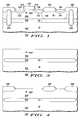
- FIG. 1illustrates a cross section of a lateral PNP 100 in accordance with the teachings of the present invention. It is understood that the drawings are for purposes of illustration only and are not to scale. Illustrated is substrate 102 having a first conductivity type (p-conductivity type). Above substrate 102 is buried layer 104 of a second conduction type (n-type conduction). Two deep trenches 106 are on either side of lateral PNP 100 to provide for isolation, and reduce collector-substrate capacitance.
- collector region 108of p-type conduction.
- collector region 108is a lightly doped p region formed as a p-epitaxial layer. This collector region gives the lateral PNP of the present invention an increased Early voltage (which leads to improved amplifier gains) as well as a decreased base/collector capacitance (enhancing circuit performance).
- Adjacent to collector 108is an n-well 110 .
- N-well 110is operable to connect buried layer 104 to base region 112 and base contact 116 .
- Base region 112is formed by a low voltage (low V T ) n-type graded channel implant around a p-type implant formed as the emitter contact 118 .
- the formation of the base region 112 around the emitter contact 118is known as a halo implant.
- This type of base region 112leads to a high lateral PNP current gain compared to conventional lateral PNP due to the proper combination of base width and base doping.
- Collector contact 120is surrounded by a p-type conduction region 122 implanted as a graded channel implant (and is also a halo implant).
- the p-type graded channel region 122helps to reduce the Kirk effect by increasing the doping in the collector region.
- An n-type conduction region 114is implanted around the base contact 116 as a halo implant. This increases the doping near the base contact 116 and leads to increased conductivity.
- a poly-silicon gate 124with spacer 125 .
- Field oxide layer 126provides for isolation between active regions where the collector contact 120 , the emitter contact 118 , base contact 116 and gate 124 are formed.
- lateral PNP 100 of the present inventionexhibits an increased Early voltage due to the lightly doped p collector region and has a narrow base width due to the n-type graded channel implant for base region 112 , which improves the current gain over prior designs.
- This improved lateral PNPovercomes the disadvantages of other lateral PNPs.
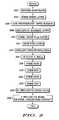
- FIG. 2is a flow chart illustrating a method of manufacturing a lateral PNP in accordance with the teachings of the present invention. The method will discuss the manufacture of a lateral PNP. While the lateral PNP is formed, other components are manufactured, such as NMOS and/or PMOS may be formed simultaneously on the same substrate. In the present invention, the lateral PNP is formed without adding additional process steps to those required to make the other devices. Therefore, no additional masks are needed for photolithography, resulting in a cost-effective process.
- a suitable substrateis provided.
- the substratewill be of p conductivity type.
- an oxidation layeris applied. In one embodiment, this oxidation layer is approximately 200 angstroms in thickness.
- photoresistis deposited and, using conventional photolithography techniques, windows are opened for implanting dopants, in step 206 .
- an n-type implantis done. This implant is done using arsenic as the n-type dopant and it is used to form a n+ buried layer, which extends into the substrate. This buried layer is then subject to an annealing step, which causes it to extend further into the substrate.
- a pre-epitaxial oxide stripis added and, using various heat cycles, a lightly-doped p epitaxial layer is grown over the p substrate with the n-type buried layer extending into both the p epitaxial layer and the p substrate.
- FIG. 3illustrates this stage in the manufacturing.
- Buried layer 104lies between the p epitaxial layer 108 and substrate 102 .
- Buried layer 104isolates the p epitaxial layer 108 from the substrate 102 .
- a field oxide layeris grown over the p epitaxial layer in every place except where device contacts and gates will be built.
- the field oxide layerwhich is a layer of silicon dioxide, is grown in the conventional manner.
- the field oxide layeris formed as follows. A layer of nitride of about 1400 angstroms is deposited over the oxidation layer and then standard photolithography techniques are used to open up windows to allow for the etching of both the nitride layer and the oxide layer. Then, the photoresist is stripped and the oxide layer is undercut under some of the nitride layer. Next, a layer of poly-silicon of about 300 angstroms in thickness is deposited as amorphous silicon.
- deep trenches 106are added.
- the deep trenchesprovide isolation and cut parasitic capacitances.
- the trenchesare formed as follows. Photolithography techniques are used to open small windows in a photoresist. Then a trench is chemically etched. Channel stop implants such as boron are added to the bottom of the trench to stop parasitic MOSFETs from turning on and the rest of the trench is filled with poly-silicon. This structure is illustrated in FIG. 5 .
- an n-well 110is formed by the implantation of phosphorous in step 216 . This is accomplished by first applying a photoresist and then using photolithography techniques, forming an opening over the area where the n-well is to be established. Then a chain implant of phosphorous is done. A chain implant is a series of implants done at different energies and is well known in the art. This allows for a deep, middle and surface implantation of phosphorous. The n-well is added in such a fashion that it extends to and touches the buried layer. After the implantation, all of the photoresist is stripped.
- the n-wellIn a conventional lateral PNP, the n-well extends through the p-epitaxial layer, resulting in a large base width. This results in a small current gain.
- the n-wellserves to connect the base to the buried layer and base contact so it does not effect the current gain. This structure is illustrated in FIG. 6 .
- a poly-silicon gate 124is formed. This is done by first coating with a layer of poly-silicon over a thin oxide. Then, a thin layer of nitride is added. Photoresist is added on top of the layer of nitride and, using conventional photolithography techniques, it is stripped in every area except where the gate is to be formed. Everything not covered by photoresist is then stripped to the gate oxide layer. The resist is then removed leaving the poly-silicon gate formed in the correct area. Spacers 125 are formed either side of gate 124 in a step not pictured but well known in the art. This structure is illustrated in FIG. 7 .
- an n-type graded channel region 114is added. This is done by first covering all areas with photoresist and then removing photoresist from the area where the implantation is to occur. Then, a phosphorous implantation is done to give an n-type region. This implantation is done is such a way as to leave a laterally non-uniform doping in that region which is known as a graded channel region. This will increase the n-type doping under the base contact, which will increase conductivity. This structure is illustrated in FIG. 8 .
- the base region 112is formed. It is formed in a similar way as the n-type graded channel region, which overlies the n-well. An implantation of phosphorous is done using a low threshold voltage dose to form a lightly doped n-type graded channel as the base. After diffusion, this base region will contact the n-well which will, in turn, contact the region formed in step 220 , which is in contact with the base contact as depicted in FIG. 1 .
- the advantage of this base regionis that it allows for a larger current gain over conventional lateral PNPs due to the reduced base width and the proper doping. This is illustrated in FIG. 9 .
- a p-type graded channel region 122is added. This will be formed in the area where the collector contact will be located. This is done in a similar fashion as in steps 220 and 222 .
- the dopant addedis boron to form a p-type conductivity region. This p-type graded channel region helps to reduce the Kirk effect. Again, this is illustrated in FIG. 10 .
- step 226dual n-type implants will be done—one at the gate region and the other where the n-type graded channel region in the base contact 116 is located. This forms an n-type poly-silicon gate region and forms an n-type base contact 116 . See FIG. 11 .
- step 228a p-type implant is done to form the collector 120 and emitter 118 contacts. This final step is illustrated as FIG. 12 .
Landscapes
- Bipolar Transistors (AREA)
- Bipolar Integrated Circuits (AREA)
Abstract
Description
Claims (14)
Priority Applications (1)
| Application Number | Priority Date | Filing Date | Title |
|---|---|---|---|
| US09/590,461US6551869B1 (en) | 2000-06-09 | 2000-06-09 | Lateral PNP and method of manufacture |
Applications Claiming Priority (1)
| Application Number | Priority Date | Filing Date | Title |
|---|---|---|---|
| US09/590,461US6551869B1 (en) | 2000-06-09 | 2000-06-09 | Lateral PNP and method of manufacture |
Publications (1)
| Publication Number | Publication Date |
|---|---|
| US6551869B1true US6551869B1 (en) | 2003-04-22 |
Family
ID=24362348
Family Applications (1)
| Application Number | Title | Priority Date | Filing Date |
|---|---|---|---|
| US09/590,461Expired - LifetimeUS6551869B1 (en) | 2000-06-09 | 2000-06-09 | Lateral PNP and method of manufacture |
Country Status (1)
| Country | Link |
|---|---|
| US (1) | US6551869B1 (en) |
Cited By (4)
| Publication number | Priority date | Publication date | Assignee | Title |
|---|---|---|---|---|
| US6927460B1 (en)* | 2002-02-15 | 2005-08-09 | Fairchild Semiconductor Corporation | Method and structure for BiCMOS isolated NMOS transistor |
| US20050285218A1 (en)* | 2004-06-25 | 2005-12-29 | Taiwan Semiconductor Manufacturing Co., Ltd. | Method of forming high voltage devices with retrograde well |
| US8878344B2 (en) | 2012-10-18 | 2014-11-04 | Analog Devices, Inc. | Compound semiconductor lateral PNP bipolar transistors |
| US20230062194A1 (en)* | 2021-08-27 | 2023-03-02 | Globalfoundries U.S. Inc. | Lateral bipolar transistors with gate structure aligned to extrinsic base |
Citations (17)
| Publication number | Priority date | Publication date | Assignee | Title |
|---|---|---|---|---|
| US3919005A (en)* | 1973-05-07 | 1975-11-11 | Fairchild Camera Instr Co | Method for fabricating double-diffused, lateral transistor |
| US4005470A (en)* | 1974-07-15 | 1977-01-25 | Signetics Corporation | Triple diffused logic elements |
| US4115797A (en)* | 1976-10-04 | 1978-09-19 | Fairchild Camera And Instrument Corporation | Integrated injection logic with heavily doped injector base self-aligned with injector emitter and collector |
| US4180827A (en)* | 1977-08-31 | 1979-12-25 | International Business Machines Corporation | NPN/PNP Fabrication process with improved alignment |
| US4203126A (en)* | 1975-11-13 | 1980-05-13 | Siliconix, Inc. | CMOS structure and method utilizing retarded electric field for minimum latch-up |
| JPS5681969A (en)* | 1979-12-08 | 1981-07-04 | Chiyou Lsi Gijutsu Kenkyu Kumiai | Manufacture of semiconductor device |
| US4458158A (en)* | 1979-03-12 | 1984-07-03 | Sprague Electric Company | IC Including small signal and power devices |
| US4484388A (en)* | 1982-06-23 | 1984-11-27 | Tokyo Shibaura Denki Kabushiki Kaishi | Method for manufacturing semiconductor Bi-CMOS device |
| US4740821A (en)* | 1986-03-21 | 1988-04-26 | Sgs Microelettronica S.P.A. | NPN equivalent structure with breakdown voltage greater than the intrinsic breakdown voltage of NPN transistors |
| US4956305A (en)* | 1986-05-30 | 1990-09-11 | Telefunken Electronic Gmbh | Process for fabricating an integrated circuit |
| US5016075A (en)* | 1988-10-14 | 1991-05-14 | Nec Corporation | Semiconductor memory device |
| US5066602A (en)* | 1982-04-19 | 1991-11-19 | Matsushita Electric Industrial Co., Ltd. | Method of making semiconductor ic including polar transistors |
| US5302534A (en)* | 1992-03-02 | 1994-04-12 | Motorola, Inc. | Forming a vertical PNP transistor |
| US5929506A (en)* | 1996-12-06 | 1999-07-27 | Texas Instrument Incorporated | Isolated vertical PNP transistor and methods for making same in a digital BiCMOS process |
| US6005283A (en)* | 1996-10-11 | 1999-12-21 | Samsung Electronics Co., Ltd. | Complementary bipolar transistors |
| US6034413A (en)* | 1997-02-27 | 2000-03-07 | Texas Instruments Incorporated | High speed biCMOS gate power for power MOSFETs incorporating improved injection immunity |
| US20010000413A1 (en)* | 1997-05-30 | 2001-04-26 | Angelo Pinto | PNP lateral bipolar electronic device |
- 2000
- 2000-06-09USUS09/590,461patent/US6551869B1/ennot_activeExpired - Lifetime
Patent Citations (17)
| Publication number | Priority date | Publication date | Assignee | Title |
|---|---|---|---|---|
| US3919005A (en)* | 1973-05-07 | 1975-11-11 | Fairchild Camera Instr Co | Method for fabricating double-diffused, lateral transistor |
| US4005470A (en)* | 1974-07-15 | 1977-01-25 | Signetics Corporation | Triple diffused logic elements |
| US4203126A (en)* | 1975-11-13 | 1980-05-13 | Siliconix, Inc. | CMOS structure and method utilizing retarded electric field for minimum latch-up |
| US4115797A (en)* | 1976-10-04 | 1978-09-19 | Fairchild Camera And Instrument Corporation | Integrated injection logic with heavily doped injector base self-aligned with injector emitter and collector |
| US4180827A (en)* | 1977-08-31 | 1979-12-25 | International Business Machines Corporation | NPN/PNP Fabrication process with improved alignment |
| US4458158A (en)* | 1979-03-12 | 1984-07-03 | Sprague Electric Company | IC Including small signal and power devices |
| JPS5681969A (en)* | 1979-12-08 | 1981-07-04 | Chiyou Lsi Gijutsu Kenkyu Kumiai | Manufacture of semiconductor device |
| US5066602A (en)* | 1982-04-19 | 1991-11-19 | Matsushita Electric Industrial Co., Ltd. | Method of making semiconductor ic including polar transistors |
| US4484388A (en)* | 1982-06-23 | 1984-11-27 | Tokyo Shibaura Denki Kabushiki Kaishi | Method for manufacturing semiconductor Bi-CMOS device |
| US4740821A (en)* | 1986-03-21 | 1988-04-26 | Sgs Microelettronica S.P.A. | NPN equivalent structure with breakdown voltage greater than the intrinsic breakdown voltage of NPN transistors |
| US4956305A (en)* | 1986-05-30 | 1990-09-11 | Telefunken Electronic Gmbh | Process for fabricating an integrated circuit |
| US5016075A (en)* | 1988-10-14 | 1991-05-14 | Nec Corporation | Semiconductor memory device |
| US5302534A (en)* | 1992-03-02 | 1994-04-12 | Motorola, Inc. | Forming a vertical PNP transistor |
| US6005283A (en)* | 1996-10-11 | 1999-12-21 | Samsung Electronics Co., Ltd. | Complementary bipolar transistors |
| US5929506A (en)* | 1996-12-06 | 1999-07-27 | Texas Instrument Incorporated | Isolated vertical PNP transistor and methods for making same in a digital BiCMOS process |
| US6034413A (en)* | 1997-02-27 | 2000-03-07 | Texas Instruments Incorporated | High speed biCMOS gate power for power MOSFETs incorporating improved injection immunity |
| US20010000413A1 (en)* | 1997-05-30 | 2001-04-26 | Angelo Pinto | PNP lateral bipolar electronic device |
Cited By (7)
| Publication number | Priority date | Publication date | Assignee | Title |
|---|---|---|---|---|
| US6927460B1 (en)* | 2002-02-15 | 2005-08-09 | Fairchild Semiconductor Corporation | Method and structure for BiCMOS isolated NMOS transistor |
| US20050285218A1 (en)* | 2004-06-25 | 2005-12-29 | Taiwan Semiconductor Manufacturing Co., Ltd. | Method of forming high voltage devices with retrograde well |
| US7221021B2 (en)* | 2004-06-25 | 2007-05-22 | Taiwan Semiconductor Manufacturing Co., Ltd. | Method of forming high voltage devices with retrograde well |
| US8878344B2 (en) | 2012-10-18 | 2014-11-04 | Analog Devices, Inc. | Compound semiconductor lateral PNP bipolar transistors |
| US20230062194A1 (en)* | 2021-08-27 | 2023-03-02 | Globalfoundries U.S. Inc. | Lateral bipolar transistors with gate structure aligned to extrinsic base |
| US11949004B2 (en)* | 2021-08-27 | 2024-04-02 | Globalfoundries U.S. Inc. | Lateral bipolar transistors with gate structure aligned to extrinsic base |
| US12349375B2 (en) | 2021-08-27 | 2025-07-01 | Globalfoundries U.S. Inc. | Lateral bipolar transistors with gate structure aligned to extrinsic base |
Similar Documents
| Publication | Publication Date | Title |
|---|---|---|
| EP0476380B1 (en) | Self-aligned bipolar transistor structure and fabrication process | |
| US5294823A (en) | SOI BICMOS process | |
| JP3205361B2 (en) | Method for manufacturing power MOS transistor with longitudinal current | |
| US4897703A (en) | Recessed contact bipolar transistor and method | |
| US4902639A (en) | Process for making BiCMOS integrated circuit having a shallow trench bipolar transistor with vertical base contacts | |
| JPH04226066A (en) | BICMOS device and its manufacturing method | |
| JPH104198A (en) | Semiconductor transistor on silicon with halo injection | |
| EP0694963B1 (en) | A method for fabricating BiCMOS semiconductor devices | |
| JP2009016856A (en) | Merged bipolar and CMOS circuits and their manufacturing methods | |
| EP0435257A2 (en) | Fabrication method for biMOS semiconductor device with improved speed and reliability | |
| US4985744A (en) | Method for forming a recessed contact bipolar transistor and field effect transistor | |
| JP2970637B2 (en) | Dielectric-isolated bipolar transistor | |
| KR100554465B1 (en) | Silicon wafer silicon element embodied on a SOI substrate and a method of manufacturing the same | |
| JPH04226064A (en) | Interconnect for semiconductor device and method for manufacturing same | |
| US5037768A (en) | Method of fabricating a double polysilicon bipolar transistor which is compatible with a method of fabricating CMOS transistors | |
| US4983531A (en) | Method of fabricating a single polysilicon bipolar transistor which is compatible with a method of fabricating CMOS transistors | |
| US5208169A (en) | Method of forming high voltage bipolar transistor for a BICMOS integrated circuit | |
| US5348896A (en) | Method for fabricating a BiCMOS device | |
| JPH10275871A (en) | Method for manufacturing semiconductor device | |
| JP4444786B2 (en) | BiCMOS manufacturing method | |
| US6551869B1 (en) | Lateral PNP and method of manufacture | |
| US5541134A (en) | Bicmos process that supports merged devices | |
| EP0656660B1 (en) | BiCMOS process | |
| US4927775A (en) | Method of fabricating a high performance bipolar and MOS device | |
| US20090114950A1 (en) | Semiconductor Device and Method of Manufacturing such a Device |
Legal Events
| Date | Code | Title | Description |
|---|---|---|---|
| AS | Assignment | Owner name:MOTOROLA, INC., ILLINOIS Free format text:ASSIGNMENT OF ASSIGNORS INTEREST;ASSIGNORS:CHAI, FRANCIS K.;BURGER, VIDA ILDEREM;KYONO, CARL S.;AND OTHERS;REEL/FRAME:011282/0869;SIGNING DATES FROM 20001016 TO 20001020 | |
| STCF | Information on status: patent grant | Free format text:PATENTED CASE | |
| AS | Assignment | Owner name:FREESCALE SEMICONDUCTOR, INC., TEXAS Free format text:ASSIGNMENT OF ASSIGNORS INTEREST;ASSIGNOR:MOTOROLA, INC.;REEL/FRAME:015698/0657 Effective date:20040404 Owner name:FREESCALE SEMICONDUCTOR, INC.,TEXAS Free format text:ASSIGNMENT OF ASSIGNORS INTEREST;ASSIGNOR:MOTOROLA, INC.;REEL/FRAME:015698/0657 Effective date:20040404 | |
| FPAY | Fee payment | Year of fee payment:4 | |
| AS | Assignment | Owner name:CITIBANK, N.A. AS COLLATERAL AGENT, NEW YORK Free format text:SECURITY AGREEMENT;ASSIGNORS:FREESCALE SEMICONDUCTOR, INC.;FREESCALE ACQUISITION CORPORATION;FREESCALE ACQUISITION HOLDINGS CORP.;AND OTHERS;REEL/FRAME:018855/0129 Effective date:20061201 Owner name:CITIBANK, N.A. AS COLLATERAL AGENT,NEW YORK Free format text:SECURITY AGREEMENT;ASSIGNORS:FREESCALE SEMICONDUCTOR, INC.;FREESCALE ACQUISITION CORPORATION;FREESCALE ACQUISITION HOLDINGS CORP.;AND OTHERS;REEL/FRAME:018855/0129 Effective date:20061201 | |
| AS | Assignment | Owner name:CITIBANK, N.A., AS COLLATERAL AGENT,NEW YORK Free format text:SECURITY AGREEMENT;ASSIGNOR:FREESCALE SEMICONDUCTOR, INC.;REEL/FRAME:024397/0001 Effective date:20100413 Owner name:CITIBANK, N.A., AS COLLATERAL AGENT, NEW YORK Free format text:SECURITY AGREEMENT;ASSIGNOR:FREESCALE SEMICONDUCTOR, INC.;REEL/FRAME:024397/0001 Effective date:20100413 | |
| FPAY | Fee payment | Year of fee payment:8 | |
| AS | Assignment | Owner name:CITIBANK, N.A., AS NOTES COLLATERAL AGENT, NEW YORK Free format text:SECURITY AGREEMENT;ASSIGNOR:FREESCALE SEMICONDUCTOR, INC.;REEL/FRAME:030633/0424 Effective date:20130521 Owner name:CITIBANK, N.A., AS NOTES COLLATERAL AGENT, NEW YOR Free format text:SECURITY AGREEMENT;ASSIGNOR:FREESCALE SEMICONDUCTOR, INC.;REEL/FRAME:030633/0424 Effective date:20130521 | |
| AS | Assignment | Owner name:CITIBANK, N.A., AS NOTES COLLATERAL AGENT, NEW YORK Free format text:SECURITY AGREEMENT;ASSIGNOR:FREESCALE SEMICONDUCTOR, INC.;REEL/FRAME:031591/0266 Effective date:20131101 Owner name:CITIBANK, N.A., AS NOTES COLLATERAL AGENT, NEW YOR Free format text:SECURITY AGREEMENT;ASSIGNOR:FREESCALE SEMICONDUCTOR, INC.;REEL/FRAME:031591/0266 Effective date:20131101 | |
| FPAY | Fee payment | Year of fee payment:12 | |
| AS | Assignment | Owner name:FREESCALE SEMICONDUCTOR, INC., TEXAS Free format text:PATENT RELEASE;ASSIGNOR:CITIBANK, N.A., AS COLLATERAL AGENT;REEL/FRAME:037356/0143 Effective date:20151207 Owner name:FREESCALE SEMICONDUCTOR, INC., TEXAS Free format text:PATENT RELEASE;ASSIGNOR:CITIBANK, N.A., AS COLLATERAL AGENT;REEL/FRAME:037354/0225 Effective date:20151207 Owner name:FREESCALE SEMICONDUCTOR, INC., TEXAS Free format text:PATENT RELEASE;ASSIGNOR:CITIBANK, N.A., AS COLLATERAL AGENT;REEL/FRAME:037356/0553 Effective date:20151207 | |
| AS | Assignment | Owner name:MORGAN STANLEY SENIOR FUNDING, INC., MARYLAND Free format text:ASSIGNMENT AND ASSUMPTION OF SECURITY INTEREST IN PATENTS;ASSIGNOR:CITIBANK, N.A.;REEL/FRAME:037486/0517 Effective date:20151207 | |
| AS | Assignment | Owner name:MORGAN STANLEY SENIOR FUNDING, INC., MARYLAND Free format text:ASSIGNMENT AND ASSUMPTION OF SECURITY INTEREST IN PATENTS;ASSIGNOR:CITIBANK, N.A.;REEL/FRAME:037518/0292 Effective date:20151207 | |
| AS | Assignment | Owner name:MORGAN STANLEY SENIOR FUNDING, INC., MARYLAND Free format text:SUPPLEMENT TO THE SECURITY AGREEMENT;ASSIGNOR:FREESCALE SEMICONDUCTOR, INC.;REEL/FRAME:039138/0001 Effective date:20160525 | |
| AS | Assignment | Owner name:NXP, B.V., F/K/A FREESCALE SEMICONDUCTOR, INC., NETHERLANDS Free format text:RELEASE BY SECURED PARTY;ASSIGNOR:MORGAN STANLEY SENIOR FUNDING, INC.;REEL/FRAME:040925/0001 Effective date:20160912 Owner name:NXP, B.V., F/K/A FREESCALE SEMICONDUCTOR, INC., NE Free format text:RELEASE BY SECURED PARTY;ASSIGNOR:MORGAN STANLEY SENIOR FUNDING, INC.;REEL/FRAME:040925/0001 Effective date:20160912 | |
| AS | Assignment | Owner name:NXP B.V., NETHERLANDS Free format text:RELEASE BY SECURED PARTY;ASSIGNOR:MORGAN STANLEY SENIOR FUNDING, INC.;REEL/FRAME:040928/0001 Effective date:20160622 | |
| AS | Assignment | Owner name:NXP USA, INC., TEXAS Free format text:CHANGE OF NAME;ASSIGNOR:FREESCALE SEMICONDUCTOR INC.;REEL/FRAME:040652/0180 Effective date:20161107 | |
| AS | Assignment | Owner name:NXP USA, INC., TEXAS Free format text:CORRECTIVE ASSIGNMENT TO CORRECT THE NATURE OF CONVEYANCE LISTED CHANGE OF NAME SHOULD BE MERGER AND CHANGE PREVIOUSLY RECORDED AT REEL: 040652 FRAME: 0180. ASSIGNOR(S) HEREBY CONFIRMS THE MERGER AND CHANGE OF NAME;ASSIGNOR:FREESCALE SEMICONDUCTOR INC.;REEL/FRAME:041354/0148 Effective date:20161107 | |
| AS | Assignment | Owner name:MORGAN STANLEY SENIOR FUNDING, INC., MARYLAND Free format text:CORRECTIVE ASSIGNMENT TO CORRECT THE REMOVE PATENTS 8108266 AND 8062324 AND REPLACE THEM WITH 6108266 AND 8060324 PREVIOUSLY RECORDED ON REEL 037518 FRAME 0292. ASSIGNOR(S) HEREBY CONFIRMS THE ASSIGNMENT AND ASSUMPTION OF SECURITY INTEREST IN PATENTS;ASSIGNOR:CITIBANK, N.A.;REEL/FRAME:041703/0536 Effective date:20151207 | |
| AS | Assignment | Owner name:SHENZHEN XINGUODU TECHNOLOGY CO., LTD., CHINA Free format text:CORRECTIVE ASSIGNMENT TO CORRECT THE TO CORRECT THE APPLICATION NO. FROM 13,883,290 TO 13,833,290 PREVIOUSLY RECORDED ON REEL 041703 FRAME 0536. ASSIGNOR(S) HEREBY CONFIRMS THE THE ASSIGNMENT AND ASSUMPTION OF SECURITYINTEREST IN PATENTS.;ASSIGNOR:MORGAN STANLEY SENIOR FUNDING, INC.;REEL/FRAME:048734/0001 Effective date:20190217 | |
| AS | Assignment | Owner name:NXP B.V., NETHERLANDS Free format text:RELEASE BY SECURED PARTY;ASSIGNOR:MORGAN STANLEY SENIOR FUNDING, INC.;REEL/FRAME:050744/0097 Effective date:20190903 | |
| AS | Assignment | Owner name:MORGAN STANLEY SENIOR FUNDING, INC., MARYLAND Free format text:CORRECTIVE ASSIGNMENT TO CORRECT THE REMOVE APPLICATION11759915 AND REPLACE IT WITH APPLICATION 11759935 PREVIOUSLY RECORDED ON REEL 037486 FRAME 0517. ASSIGNOR(S) HEREBY CONFIRMS THE ASSIGNMENT AND ASSUMPTION OF SECURITYINTEREST IN PATENTS;ASSIGNOR:CITIBANK, N.A.;REEL/FRAME:053547/0421 Effective date:20151207 | |
| AS | Assignment | Owner name:NXP B.V., NETHERLANDS Free format text:CORRECTIVE ASSIGNMENT TO CORRECT THE REMOVEAPPLICATION 11759915 AND REPLACE IT WITH APPLICATION11759935 PREVIOUSLY RECORDED ON REEL 040928 FRAME 0001. ASSIGNOR(S) HEREBY CONFIRMS THE RELEASE OF SECURITYINTEREST;ASSIGNOR:MORGAN STANLEY SENIOR FUNDING, INC.;REEL/FRAME:052915/0001 Effective date:20160622 | |
| AS | Assignment | Owner name:NXP, B.V. F/K/A FREESCALE SEMICONDUCTOR, INC., NETHERLANDS Free format text:CORRECTIVE ASSIGNMENT TO CORRECT THE REMOVEAPPLICATION 11759915 AND REPLACE IT WITH APPLICATION11759935 PREVIOUSLY RECORDED ON REEL 040925 FRAME 0001. ASSIGNOR(S) HEREBY CONFIRMS THE RELEASE OF SECURITYINTEREST;ASSIGNOR:MORGAN STANLEY SENIOR FUNDING, INC.;REEL/FRAME:052917/0001 Effective date:20160912 |