US6551399B1 - Fully integrated process for MIM capacitors using atomic layer deposition - Google Patents
Fully integrated process for MIM capacitors using atomic layer depositionDownload PDFInfo
- Publication number
- US6551399B1 US6551399B1US09/480,804US48080400AUS6551399B1US 6551399 B1US6551399 B1US 6551399B1US 48080400 AUS48080400 AUS 48080400AUS 6551399 B1US6551399 B1US 6551399B1
- Authority
- US
- United States
- Prior art keywords
- layer
- depositing
- deposition
- ald
- metal
- Prior art date
- Legal status (The legal status is an assumption and is not a legal conclusion. Google has not performed a legal analysis and makes no representation as to the accuracy of the status listed.)
- Expired - Fee Related
Links
Images


Classifications
- H—ELECTRICITY
- H10—SEMICONDUCTOR DEVICES; ELECTRIC SOLID-STATE DEVICES NOT OTHERWISE PROVIDED FOR
- H10D—INORGANIC ELECTRIC SEMICONDUCTOR DEVICES
- H10D1/00—Resistors, capacitors or inductors
- H10D1/60—Capacitors
- H10D1/68—Capacitors having no potential barriers
- C—CHEMISTRY; METALLURGY
- C23—COATING METALLIC MATERIAL; COATING MATERIAL WITH METALLIC MATERIAL; CHEMICAL SURFACE TREATMENT; DIFFUSION TREATMENT OF METALLIC MATERIAL; COATING BY VACUUM EVAPORATION, BY SPUTTERING, BY ION IMPLANTATION OR BY CHEMICAL VAPOUR DEPOSITION, IN GENERAL; INHIBITING CORROSION OF METALLIC MATERIAL OR INCRUSTATION IN GENERAL
- C23C—COATING METALLIC MATERIAL; COATING MATERIAL WITH METALLIC MATERIAL; SURFACE TREATMENT OF METALLIC MATERIAL BY DIFFUSION INTO THE SURFACE, BY CHEMICAL CONVERSION OR SUBSTITUTION; COATING BY VACUUM EVAPORATION, BY SPUTTERING, BY ION IMPLANTATION OR BY CHEMICAL VAPOUR DEPOSITION, IN GENERAL
- C23C16/00—Chemical coating by decomposition of gaseous compounds, without leaving reaction products of surface material in the coating, i.e. chemical vapour deposition [CVD] processes
- C23C16/02—Pretreatment of the material to be coated
- C23C16/0227—Pretreatment of the material to be coated by cleaning or etching
- C23C16/0236—Pretreatment of the material to be coated by cleaning or etching by etching with a reactive gas
- C—CHEMISTRY; METALLURGY
- C23—COATING METALLIC MATERIAL; COATING MATERIAL WITH METALLIC MATERIAL; CHEMICAL SURFACE TREATMENT; DIFFUSION TREATMENT OF METALLIC MATERIAL; COATING BY VACUUM EVAPORATION, BY SPUTTERING, BY ION IMPLANTATION OR BY CHEMICAL VAPOUR DEPOSITION, IN GENERAL; INHIBITING CORROSION OF METALLIC MATERIAL OR INCRUSTATION IN GENERAL
- C23C—COATING METALLIC MATERIAL; COATING MATERIAL WITH METALLIC MATERIAL; SURFACE TREATMENT OF METALLIC MATERIAL BY DIFFUSION INTO THE SURFACE, BY CHEMICAL CONVERSION OR SUBSTITUTION; COATING BY VACUUM EVAPORATION, BY SPUTTERING, BY ION IMPLANTATION OR BY CHEMICAL VAPOUR DEPOSITION, IN GENERAL
- C23C16/00—Chemical coating by decomposition of gaseous compounds, without leaving reaction products of surface material in the coating, i.e. chemical vapour deposition [CVD] processes
- C23C16/44—Chemical coating by decomposition of gaseous compounds, without leaving reaction products of surface material in the coating, i.e. chemical vapour deposition [CVD] processes characterised by the method of coating
- C23C16/455—Chemical coating by decomposition of gaseous compounds, without leaving reaction products of surface material in the coating, i.e. chemical vapour deposition [CVD] processes characterised by the method of coating characterised by the method used for introducing gases into reaction chamber or for modifying gas flows in reaction chamber
- C23C16/45523—Pulsed gas flow or change of composition over time
- C23C16/45525—Atomic layer deposition [ALD]
- C23C16/45527—Atomic layer deposition [ALD] characterized by the ALD cycle, e.g. different flows or temperatures during half-reactions, unusual pulsing sequence, use of precursor mixtures or auxiliary reactants or activations
- C23C16/45529—Atomic layer deposition [ALD] characterized by the ALD cycle, e.g. different flows or temperatures during half-reactions, unusual pulsing sequence, use of precursor mixtures or auxiliary reactants or activations specially adapted for making a layer stack of alternating different compositions or gradient compositions
- C—CHEMISTRY; METALLURGY
- C23—COATING METALLIC MATERIAL; COATING MATERIAL WITH METALLIC MATERIAL; CHEMICAL SURFACE TREATMENT; DIFFUSION TREATMENT OF METALLIC MATERIAL; COATING BY VACUUM EVAPORATION, BY SPUTTERING, BY ION IMPLANTATION OR BY CHEMICAL VAPOUR DEPOSITION, IN GENERAL; INHIBITING CORROSION OF METALLIC MATERIAL OR INCRUSTATION IN GENERAL
- C23C—COATING METALLIC MATERIAL; COATING MATERIAL WITH METALLIC MATERIAL; SURFACE TREATMENT OF METALLIC MATERIAL BY DIFFUSION INTO THE SURFACE, BY CHEMICAL CONVERSION OR SUBSTITUTION; COATING BY VACUUM EVAPORATION, BY SPUTTERING, BY ION IMPLANTATION OR BY CHEMICAL VAPOUR DEPOSITION, IN GENERAL
- C23C16/00—Chemical coating by decomposition of gaseous compounds, without leaving reaction products of surface material in the coating, i.e. chemical vapour deposition [CVD] processes
- C23C16/44—Chemical coating by decomposition of gaseous compounds, without leaving reaction products of surface material in the coating, i.e. chemical vapour deposition [CVD] processes characterised by the method of coating
- C23C16/455—Chemical coating by decomposition of gaseous compounds, without leaving reaction products of surface material in the coating, i.e. chemical vapour deposition [CVD] processes characterised by the method of coating characterised by the method used for introducing gases into reaction chamber or for modifying gas flows in reaction chamber
- C23C16/45561—Gas plumbing upstream of the reaction chamber
- H—ELECTRICITY
- H01—ELECTRIC ELEMENTS
- H01L—SEMICONDUCTOR DEVICES NOT COVERED BY CLASS H10
- H01L21/00—Processes or apparatus adapted for the manufacture or treatment of semiconductor or solid state devices or of parts thereof
- H01L21/02—Manufacture or treatment of semiconductor devices or of parts thereof
- H01L21/02104—Forming layers
- H01L21/02107—Forming insulating materials on a substrate
- H01L21/02109—Forming insulating materials on a substrate characterised by the type of layer, e.g. type of material, porous/non-porous, pre-cursors, mixtures or laminates
- H01L21/02205—Forming insulating materials on a substrate characterised by the type of layer, e.g. type of material, porous/non-porous, pre-cursors, mixtures or laminates the layer being characterised by the precursor material for deposition
- H01L21/02208—Forming insulating materials on a substrate characterised by the type of layer, e.g. type of material, porous/non-porous, pre-cursors, mixtures or laminates the layer being characterised by the precursor material for deposition the precursor containing a compound comprising Si
- H01L21/02219—Forming insulating materials on a substrate characterised by the type of layer, e.g. type of material, porous/non-porous, pre-cursors, mixtures or laminates the layer being characterised by the precursor material for deposition the precursor containing a compound comprising Si the compound comprising silicon and nitrogen
- H01L21/02222—Forming insulating materials on a substrate characterised by the type of layer, e.g. type of material, porous/non-porous, pre-cursors, mixtures or laminates the layer being characterised by the precursor material for deposition the precursor containing a compound comprising Si the compound comprising silicon and nitrogen the compound being a silazane
- H—ELECTRICITY
- H01—ELECTRIC ELEMENTS
- H01L—SEMICONDUCTOR DEVICES NOT COVERED BY CLASS H10
- H01L21/00—Processes or apparatus adapted for the manufacture or treatment of semiconductor or solid state devices or of parts thereof
- H01L21/02—Manufacture or treatment of semiconductor devices or of parts thereof
- H01L21/04—Manufacture or treatment of semiconductor devices or of parts thereof the devices having potential barriers, e.g. a PN junction, depletion layer or carrier concentration layer
- H01L21/18—Manufacture or treatment of semiconductor devices or of parts thereof the devices having potential barriers, e.g. a PN junction, depletion layer or carrier concentration layer the devices having semiconductor bodies comprising elements of Group IV of the Periodic Table or AIIIBV compounds with or without impurities, e.g. doping materials
- H01L21/28—Manufacture of electrodes on semiconductor bodies using processes or apparatus not provided for in groups H01L21/20 - H01L21/268
- H01L21/283—Deposition of conductive or insulating materials for electrodes conducting electric current
- H01L21/285—Deposition of conductive or insulating materials for electrodes conducting electric current from a gas or vapour, e.g. condensation
- H01L21/28506—Deposition of conductive or insulating materials for electrodes conducting electric current from a gas or vapour, e.g. condensation of conductive layers
- H01L21/28512—Deposition of conductive or insulating materials for electrodes conducting electric current from a gas or vapour, e.g. condensation of conductive layers on semiconductor bodies comprising elements of Group IV of the Periodic Table
- H01L21/28556—Deposition of conductive or insulating materials for electrodes conducting electric current from a gas or vapour, e.g. condensation of conductive layers on semiconductor bodies comprising elements of Group IV of the Periodic Table by chemical means, e.g. CVD, LPCVD, PECVD, laser CVD
- H01L21/28562—Selective deposition
- H—ELECTRICITY
- H01—ELECTRIC ELEMENTS
- H01L—SEMICONDUCTOR DEVICES NOT COVERED BY CLASS H10
- H01L21/00—Processes or apparatus adapted for the manufacture or treatment of semiconductor or solid state devices or of parts thereof
- H01L21/02—Manufacture or treatment of semiconductor devices or of parts thereof
- H01L21/02104—Forming layers
- H01L21/02107—Forming insulating materials on a substrate
- H01L21/02109—Forming insulating materials on a substrate characterised by the type of layer, e.g. type of material, porous/non-porous, pre-cursors, mixtures or laminates
- H01L21/02112—Forming insulating materials on a substrate characterised by the type of layer, e.g. type of material, porous/non-porous, pre-cursors, mixtures or laminates characterised by the material of the layer
- H01L21/02172—Forming insulating materials on a substrate characterised by the type of layer, e.g. type of material, porous/non-porous, pre-cursors, mixtures or laminates characterised by the material of the layer the material containing at least one metal element, e.g. metal oxides, metal nitrides, metal oxynitrides or metal carbides
- H01L21/02175—Forming insulating materials on a substrate characterised by the type of layer, e.g. type of material, porous/non-porous, pre-cursors, mixtures or laminates characterised by the material of the layer the material containing at least one metal element, e.g. metal oxides, metal nitrides, metal oxynitrides or metal carbides characterised by the metal
- H01L21/02178—Forming insulating materials on a substrate characterised by the type of layer, e.g. type of material, porous/non-porous, pre-cursors, mixtures or laminates characterised by the material of the layer the material containing at least one metal element, e.g. metal oxides, metal nitrides, metal oxynitrides or metal carbides characterised by the metal the material containing aluminium, e.g. Al2O3
- H—ELECTRICITY
- H01—ELECTRIC ELEMENTS
- H01L—SEMICONDUCTOR DEVICES NOT COVERED BY CLASS H10
- H01L21/00—Processes or apparatus adapted for the manufacture or treatment of semiconductor or solid state devices or of parts thereof
- H01L21/02—Manufacture or treatment of semiconductor devices or of parts thereof
- H01L21/02104—Forming layers
- H01L21/02107—Forming insulating materials on a substrate
- H01L21/02109—Forming insulating materials on a substrate characterised by the type of layer, e.g. type of material, porous/non-porous, pre-cursors, mixtures or laminates
- H01L21/02112—Forming insulating materials on a substrate characterised by the type of layer, e.g. type of material, porous/non-porous, pre-cursors, mixtures or laminates characterised by the material of the layer
- H01L21/02172—Forming insulating materials on a substrate characterised by the type of layer, e.g. type of material, porous/non-porous, pre-cursors, mixtures or laminates characterised by the material of the layer the material containing at least one metal element, e.g. metal oxides, metal nitrides, metal oxynitrides or metal carbides
- H01L21/02175—Forming insulating materials on a substrate characterised by the type of layer, e.g. type of material, porous/non-porous, pre-cursors, mixtures or laminates characterised by the material of the layer the material containing at least one metal element, e.g. metal oxides, metal nitrides, metal oxynitrides or metal carbides characterised by the metal
- H01L21/02183—Forming insulating materials on a substrate characterised by the type of layer, e.g. type of material, porous/non-porous, pre-cursors, mixtures or laminates characterised by the material of the layer the material containing at least one metal element, e.g. metal oxides, metal nitrides, metal oxynitrides or metal carbides characterised by the metal the material containing tantalum, e.g. Ta2O5
- H—ELECTRICITY
- H01—ELECTRIC ELEMENTS
- H01L—SEMICONDUCTOR DEVICES NOT COVERED BY CLASS H10
- H01L21/00—Processes or apparatus adapted for the manufacture or treatment of semiconductor or solid state devices or of parts thereof
- H01L21/02—Manufacture or treatment of semiconductor devices or of parts thereof
- H01L21/02104—Forming layers
- H01L21/02107—Forming insulating materials on a substrate
- H01L21/02225—Forming insulating materials on a substrate characterised by the process for the formation of the insulating layer
- H01L21/0226—Forming insulating materials on a substrate characterised by the process for the formation of the insulating layer formation by a deposition process
- H01L21/02263—Forming insulating materials on a substrate characterised by the process for the formation of the insulating layer formation by a deposition process deposition from the gas or vapour phase
- H01L21/02271—Forming insulating materials on a substrate characterised by the process for the formation of the insulating layer formation by a deposition process deposition from the gas or vapour phase deposition by decomposition or reaction of gaseous or vapour phase compounds, i.e. chemical vapour deposition
- H01L21/0228—Forming insulating materials on a substrate characterised by the process for the formation of the insulating layer formation by a deposition process deposition from the gas or vapour phase deposition by decomposition or reaction of gaseous or vapour phase compounds, i.e. chemical vapour deposition deposition by cyclic CVD, e.g. ALD, ALE, pulsed CVD
Definitions
- the present inventionrelates generally to semiconductor technology and, more particularly, to a method and apparatus for manufacturing metal-insulator-metal capacitors using atomic layer deposition.
- CVDchemical vapor deposition
- its variant processesare utilized to deposit thin films of uniform and, often times conformal coatings over high-aspect and uneven features present on a wafer.
- new processesare needed to deposit ultrathin film layers on a wafer.
- the standard CVD techniqueshave difficulty meeting the uniformity and conformity requirements for much thinner films.
- ALDatomic layer deposition
- ALDhas its roots originally in atomic layer epitaxy, which is described in U.S. Pat. Nos. 4,058,430 and 4,413,022 and in an article titled “Atomic Layer Epitaxy” by Goodman et al., J. Appl. Phys. 60(3), Aug. 1, 1986; pp. R65-R80.
- ALDis a process wherein conventional CVD processes are divided into single-monolayer depositions, wherein each separate deposition step theoretically reaches saturation at a single molecular or atomic monolayer thickness and, then, self-terminates.
- the depositionis an outcome of chemical reactions between reactive molecular precursors and the substrate (either the base substrate or layers formed on the base substrate).
- the elements comprising the filmare delivered as molecular precursors.
- the desired net reactionis to deposit a pure film and eliminate “extra” atoms (molecules) that comprise the molecular precursors (ligands).
- the precursorsare fed simultaneously into the reactor.
- the precursorsare introduced into the reactor separately, typically by alternating the flow, so that only one precursor at a time is introduced into the reactor.
- the first precursorcould be a metal precursor containing a metal element M, which is bonded to an atomic or molecular ligand L to form a volatile molecule ML x .
- the metal precursorreacts with the substrate to deposit a monolayer of the metal M with its passivating ligand.
- the chamberis purged and, then, followed by an introduction of a second precursor.
- the second precursoris introduced to restore the surface reactivity towards the metal precursor for depositing the next layer of metal.
- MIM capacitorsare implemented by a sequence that includes bottom metal deposition, patterning, dielectric deposition, top metal deposition and patterning. MIM capacitors are utilized in a variety of devices, including memory devices (such as dynamic random-access-memory, or DRAM). The general use of MIM capacitors in integrated circuits and RF circuits is known in the art.
- ALDatomic layer deposition
- a defined structureis then formed by removing portions of the first conductive and sacrificial layers.
- the sacrificial layeris removed to expose the underlying first conductive layer without exposing the first conductive layer to oxidation.
- a dielectric layeris next deposited over the exposed first conductive layer by atomic layer deposition.
- MIMmetal-insulator-metal
- FIG. 1is a cross-sectional diagram showing an embodiment of the present invention in forming a bottom conductive layer of a metal-insulator-metal (MIM) capacitor above a substrate in which an overlying sacrificial layer is also deposited to cover the bottom conductive layer.
- MIMmetal-insulator-metal
- FIG. 2is a cross-sectional diagram showing the patterning and etching of the structure of FIG. 1 to define the MIM capacitor stack.
- FIG. 3is a cross-sectional diagram showing a removal of the sacrificial layer of FIG. 2 and subsequent deposition of a dielectric layer and a top conductive layer of the MIM capacitor.
- FIG. 4is a cross-sectional diagram showing the final formation of the MIM capacitor stack from the structure of FIG. 3 .
- FIG. 5is a cross-sectional diagram showing another embodiment of the present invention in pretreating a substrate to make it more reactive, forming an adhesion layer above the substrate, forming a bottom conductive layer of a metal-insulator-metal (MIM) capacitor and forming an overlying sacrificial layer to cover the bottom conductive layer.
- MIMmetal-insulator-metal
- FIG. 6is a cross-sectional diagram showing the patterning and etching of the structure of FIG. 5 to define the MIM capacitor bottom electrode.
- FIG. 7is a cross-sectional diagram showing a removal of the sacrificial layer of FIG. 6 and subsequent pretreatment of the exposed surface to pretreat the surface of the bottom conductive layer for deposition of a dielectric layer.
- FIG. 8is a cross-sectional diagram showing the deposition of a dielectric layer over the pretreated structure of FIG. 7 .
- FIG. 9is a cross-sectional diagram showing a subsequent pretreatment of the dielectric layer of FIG. 8 to make the surface of the dielectric layer reactive.
- FIG. 10is a is a cross-sectional diagram showing the deposition of a top conductive layer over the dielectric layer of FIG. 9 .
- FIG. 11is a cross-sectional diagram showing the final formation of the MIM capacitor stack from the structure of FIG. 10 .
- FIGS. 12A-Billustrate a flow diagram for practicing one embodiment of the present invention.
- FIG. 13is a block diagram showing one reactor apparatus for performing ALD, as well as pretreating the surface of a layer prior to ALD, in order to fabricate an MIM capacitor practicing the present invention.
- FIG. 14is a block diagram showing a cluster tool for practicing the present invention.
- ALDatomic layer deposition
- the first precursor introducedis a metal precursor comprising a metal element M bonded to atomic or molecular ligand L to make a volatile molecule ML x (the x, y and z subscripts are utilized herein to denote integers 1, 2, 3, etc.). It is desirable that the ML x molecule bond with a ligand attached to the surface of the substrate.
- An example ligandis a hydrogen-containing ligand, such as AH, where A is a nonmetal element bonded to hydrogen.
- the desired reactionis noted as AH+ML x ⁇ AML y +HL, where HL is the exchange reaction by-product.
- the second precursorreacts with the L termination on the surface.
- the second precursoris comprised of AH z , with A being a nonmetal element.
- the hydrogen componentis typically represented by H 2 O, NH 3 or H 2 S.
- the reaction ML+AH z ⁇ MAH+HLresults in the desired additional element A being deposited as AH terminated sites and the ligand L is eliminated as a volatile by-product HL.
- the surfacenow has AH terminated sites, which restore the surface to have AH terminations. This restoration completes one ALD cycle, in which a monolayer of MA is deposited on the surface.
- the present inventionuses the ALD process to fabricate a metal-insulator-metal (MIM) capacitor on a semiconductor wafer, such as a silicon wafer.
- MIMmetal-insulator-metal
- a semiconductor wafersuch as a silicon wafer.
- a prior art techniquesuch as the generic CVD process
- pattern delineationphotolithographic patterning, etching, etc.
- cleaning stepscan oxidize the surface of the bottom conductive layer (including, metal, metal nitride or semiconducting layer).
- the extent of oxidationvaries with the substrate and the cleaning process, but typically accounts for more than 10 Angstroms.
- the air exposure of the bottom conductor during pattern delineation, as well as some oxygen plasma ashing processes that are conventionally applied to remove photoresist,will oxidize the surface of the bottom electrode, which will interface with an overlying insulator material.
- Parasitic oxide in the metal-dielectric interfaceis undesirable, since these low quality oxides do not contribute to the insulating properties of the MIM capacitor. Worse, the added thickness may reduce the capacitance value by making the effective dielectric thicker.
- these poorly defined oxidesmay interfere with surface activation of the following dielectric ALD film and deteriorate the insulating properties of the ALD dielectric film.
- a substrate 10(again, substrate is used herein to refer to either a base substrate or a material film layer formed on a base substrate) is shown upon which ALD is performed.
- a first conductive layerwhich is typically a metal (M 1 ) layer, 11 is deposited by ALD.
- M 1 layer 11is comprised of a metal or metal nitride, including Ta, Ta x N, Ti, TiN or Al, which is used for constructing MIM capacitors.
- a typical example structure for a MIMis Ta x N/Al 2 O 3 /Ta x N stack on HSG (high surface area polysilicon grain) layer.
- substrate 10can be HSG
- M 1 layer 11can be Ta x N.
- ALDM 1 layer 11 is deposited to an approximate thickness, of 30-50 angstroms.
- a sacrificial layer 12is deposited overlying layer 11 by ALD.
- the sacrificial layer 12is deposited by ALD, without oxidizing the surface of the M 1 layer 11 . Accordingly, layer 12 is deposited in the same processing chamber or in another chamber of the same cluster tool, so that M 1 layer 11 is not exposed to an oxidizing or contaminating environment.
- the sacrificial layer 12is also comprised of metal material.
- the composition of the sacrificial layershould be such that a given in situ dry etch chemistry will remove the sacrificial layer 12 , but not the underlying M 1 layer 11 .
- the thickness of the sacrificial layer deposited by ALDwill depend on other properties, but typically a thin layer in the approximate range of 20-50 Angstroms is deposited.
- the sacrificial layer 12can be comprised of material which etches in fluorine-based plasma. Accordingly, with the M 1 layer 11 being comprised of the material noted above, the sacrificial layer 12 can be comprised of W, WS x , W x N or SiO 2 , just to name a few examples. These materials will be etched by fluorine atoms.
- the sacrificial layer 12is deposited immediately after the deposition of the M 1 layer, without air exposure of the M 1 layer and without significant delay.
- the sacrificial layer 12provides a covering layer over the M 1 layer 11 .
- the waferis removed from the processing chamber (or cluster tool) for pattern delineation.
- the wafercan now be exposed to air (ambient) or other oxygen and/or contaminating environment since the M 1 layer 11 is not exposed. Since some appreciable time is required for pattern delineation, oxidation will most likely occur on the top layers of the sacrificial layer 12 , but this is permitted, since the sacrificial layer will be later removed.
- FIG. 2shows the substrate 10 having a pattern delineated stack 13 formed thereon.
- a variety of photolithographic and etching techniquescan be used to form the patterned stack 13 . Typically, anisotropic etch is used. Then, the wafer is placed back in the same or different processing chamber and subjected to an etch process. In the case of the above example, fluorine-based chemistry, such as NF 3 , is used to etch away the W-based sacrificial layer 12 , while not etching the M 1 layer 11 . This etching process exposes the underlying M 1 layer 11 of stack 13 .
- the materials for the two layers 11 , 12 and the etch chemistryshould be chosen, so that the etch chemistry is selective to remove the sacrificial layer 12 and not the M 1 layer 11 .
- a dielectric layer 14is deposited by ALD.
- the ALDdeposits a uniform and conformal layer 14 over the substrate 10 , as well as stack 13 .
- the dielectric layer 14is comprised of Al 2 O 3 .
- Al 2 O 3is deposited to a thickness in the approximate range of 15-50 Angstroms by ALD.
- the dielectric layer 14is deposited without subjecting the exposed M 1 layer to oxidation and/or contamination. That is, when the sacrificial layer is removed (etched) in a processing chamber, the wafer is processed, in the same chamber or in another chamber of the same cluster tool without being exposed to air or contamination, to deposit the dielectric layer 14 .
- a top conductive layertypically a metal (M 2 ) layer, 15 is deposited overlying the dielectric layer 14 , having a thickness as practically needed in the approximate range of 30-3000 Angstroms.
- the M 2 layercan be deposited by ALD, CVD, plasma-enhanced CVD (PECVD) or another process.
- ALDis still preferred over other processes for improved controls on the deposition of the M 2 layer 15 .
- a combination of ALD and CVDcould be used.
- the waferis patterned and etched to form the completed MIM stack 13 .
- anisotropic etchis used.
- the final MIM capacitor stack 13is comprised of the M 1 layer 11 , dielectric layer 14 and M 2 layer 15 overlying the substrate 10 . Two such stacks 13 are shown in FIG. 4 .
- ALDis used to deposit layers 11 and 14 , as well as the sacrificial layer 12 (which has been consumed). ALD can be used to deposit M 2 layer as well.
- one or more radical specie(s), including such species as oxygen, hydrogen, OH, NH 2 , Cl and F,can be introduced to react with the surface of the substrate.
- the particular species selectedwill depend on the surface chemistry.
- a given speciesis utilized to modify the surface of the substrate.
- the reactive speciespretreats the surface so that the surface is more susceptible to reacting with the precursor.
- the reactive speciestypically will modify the surface by exchanging other surface species and/or attaching to previously reconstructed sites to provide more termination sites for the precursor being utilized.
- SiO 2 surface with approximately 100% siloxane SiOSi bridgeis generally inert.
- OH, H or O radical exposurecan efficiently insert HOH into the SiOSi to generate 2 Si—OH surface species that are highly reactive with ML x molecular precursor.
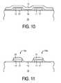
- FIGS. 5-11an alternative embodiment of the invention is shown.
- the surface of the substrate 10is pretreated prior to the deposition of the M 1 layer 11 .
- Pretreating the surface of the substrate 10results in a more reactive surface, which is shown by the formation of ample termination sites 16 on the surface of the substrate 10 .
- ML xis the first precursor for depositing the M 1 layer
- the surfaceis pretreated to have additional AH termination sites 16 present.
- an alternative techniqueis to pretreat the various surfaces to make the surface reactive prior to performing ALD.
- the surface pretreatmentcreates additional termination sites 16 .
- NH 3 /H 2 plasmais used to activate the surface of the substrate 10 .
- the M 1 layer 11could be deposited on the treated surface, several monolayers of Ta film are deposited by ALD to form an adhesion layer 17 to promote good adhesion of the M 1 metal onto the substrate.
- the composition of the adhesion film 17is dependent on the chemistries of the materials being utilized.
- Tais deposited on HSG, which has its surface activated for Ta.
- TaNis deposited by ALD to form the Ta x N (M 1 ) layer 11 to a thickness in the range of 30-50 angstroms.
- M 1the sacrificial layer 12
- the waferis unloaded and then subjected to the pattern delineation steps described above.
- the resulting MIM stack 13 ais shown in FIG. 6 .
- the waferis returned to the processing chamber and the sacrificial layer 12 is etched away, as shown in FIG. 7 .
- NF 3 plasmacan be utilized for this process.
- the M 1 layer 11is pretreated to make the surface more reactive for the dielectric deposition. The pretreatment results in having more termination sites 18 to be present on the M 1 material to react with a species of a precursor used to deposit the overlying dielectric layer.
- the dielectric layer 14is deposited above the substrate 10 and the M 1 layer 11 . Again, it is to be noted that the dielectric layer 14 is deposited without subjecting the exposed M 1 layer to oxidation and/or contamination.
- a variety of activation processesare available for pretreating the M 1 layer.
- NH 3 /H 2 /N 2 plasmais used to terminate the surface with NH x species. This plasma also eliminates the surface fluorine on the substrate surface.
- the dielectric layer 14Al 2 O 3 in this instance
- TMAtrimethyle aluminum
- Al 2 O 3is deposited to an approximate thickness of 15-50 Angstroms.
- the dielectric layer 14is pretreated to make the surface more reactive to the subsequent M 2 deposition.
- the top surface of the dielectric layer 14is activated using the NH 3 /H 2 /N 2 plasma, as shown by having ample terminations 19 .
- the M 2 layer 15is deposited on the activated surface of layer 14 .
- FIG. 10A typical material for use for the composition of the M 2 layer is W or W x N. In this instance the W or W x N is deposited by ALD on the NH 3 /H 2 /N 2 plasma activated surface of Al 2 O 3 to a thickness of approximately 30-3,000 Angstroms.
- the M 2 layer 15can be deposited by other processes, including CVD and PECVD, or a combination of ALD seed layer and CVD, PECVD or electroplating.
- FIG. 11illustrates the final stacked MIM capacitor 13 a after etching.
- the pretreatment of the various surfacescan be achieved to deposit enough radical species to exchange with the surface.
- these radical speciesprovide termination sites for bonding to a specie of the precursor.
- An intermediate layermay be required in some instances when the substrate cannot be made reactive with either of the ALD molecular precursors by a simple attachment or exchange of surface species.
- the ultra thin intermediate layeris deposited as part of the pretreatment process.
- the intermediate layerprovides a new surface that is reactive to one or both precursors.
- the layeris formed having a thickness which is kept minimal, but sufficient for activation.
- the intermediate layermay be conductive, semiconductive or insulating (dielectric). Typically, it will match the electrical properties of either the substrate or the overlying film being grown. For example, an intermediate layer is needed as a transition layer when W or WN x films are deposited on SiO 2 .
- the intermediate layerIn this instance, Al 2 O 3 (which is an insulator) or TiN, Ti, Ta or Ta x N (which are conductors) can be used for the intermediate layer.
- the adhesion layer 17also performs as an intermediate layer as well. It is to be noted further, that the intermediate layer is typically deposited by ALD for the pretreatment of the surface.
- a leaching processcan be utilized. Since some surfaces are quite inert, a process other than reactive exchange or attachment may be desirable. For example, hydrocarbon and fluorocarbon polymers are utilized for low-k dielectrics. Adhesion of films, for sealing (insulating) or for forming a barrier (metals, metal nitrides), is difficult to achieve. In these instances, leaching hydrogen or fluorine from the top layer of the polymer can activate the surface for ALD.
- ALD deposition of Al 2 O 3 on siliconA silicon substrate is first activated (pretreated) by forming thin layers of silicon oxide (SiO 2 ) or silicon oxinitride, in which OH and/or NH x groups form the terminations.
- the processinvolves O 2 /H 2 /H 2 O/NH 3 remote plasma that includes different ratios of the constituents to form the terminations prior to the introduction of the first precursor to grow the Al 2 O 3 thin film layer on silicon.
- ALD deposition of Al 2 O 3 on siliconThe silicon substrate is activated by forming thin layers of SiO 2 that is hydroxilated by exposing HF cleaned (H terminated) silicon to a pulse of H 2 O at temperatures below 430° C. This process results in a self-saturated layer of SiO 2 that is approximately 5 angstroms thick.
- ALD deposition of Al 2 O 3 on WN xNH 3 /H 2 /N 2 plasma is used to leach fluorine from the top layers of the WN x film and terminate the surface with NH x species. These species are reacted with trimethyl aluminum (TMA) to initiate deposition of Al 2 O 3 on WN x .
- TMAtrimethyl aluminum
- NH 3 /H 2 /N 2 plasmais used to terminate the surface with NH x species. These species are reacted with TMA to initiate Al 2 O 3 ALD.
- ALD deposition of Al 2 O 3 on TiNH 3 /H 2 /N 2 plasma is used to nitridize the surface and terminate the surface with NH x species. Maintain conditions to avoid extensive nitridization into the Ti film. The NH x species are reacted with TMA to initiate Al 2 O 3 ALD.
- ALD deposition of Al 2 O 3 on WNH 3 /H 2 /N 2 plasma is used to nitridize the surface and terminate the surface with NH x species. Maintain conditions to avoid extensive nitridization into the W film. The NH x species are reacted with TMA to initiate Al 2 O 3 ALD.
- ALD deposition of Al 2 O 3 on TaNH 3 /H 2 /N 2 plasma is used to nitridize the surface and terminate the surface with NH x species. Maintain conditions to avoid extensive nitridization into the Ta film. The NH x species are reacted with TMA to initiate Al 2 O 3 ALD.
- ALD deposition of Al 2 O 3 on Ta x NNH 3 /H 2 /N 2 plasma is used to terminate the surface with NH x species. The NH x species are reacted with TMA to initiate Al 2 O 3 ALD.
- ALD deposition of Ta 2 O 5 on Al 2 O 3involves O 2 /H 2 /H 2 O remote plasma that includes different ratios of the constituents. This plasma is used to terminate the surface with OH species that are reactive with TaCl 5 .
- ALD deposition of Al 2 O 3 on Ta 2 O 5involves O 2 /H 2 /H 2 O remote plasma that includes different ratios of the constituents. This plasma is used to terminate the surface with OH species that are reactive with TaCl 5 .
- ALD deposition of TiO x on Al 2 O 3involves O 2 /H 2 /H 2 O remote plasma that includes different ratios of the constituents. This plasma is used to terminate the surface with OH species that are reactive with TMA.
- ALD deposition of Al 2 O 3 on TiO xinvolves O 2 /H 2 /H 2 O remote plasma that includes different ratios of the constituents. This plasma is used to terminate the surface with OH species that are reactive with TiCl 4 .
- NH 3 /H 2 /N 2 plasmais used to terminate the surface with NH x species.
- the NH x speciesare reacted with TiCl 4 to initiate TiO x ALD.
- ALD deposition of W on TiNNH 3 /H 2 /N 2 plasma is used to terminate the surface with NH x species.
- the NH x speciesare reacted with TiCl 4 to initiate TiN ALD.
- ALD deposition of WN x on TiNNH 3 /H 2 /N 2 plasma is used to terminate the surface with NH x species. The NH x species are reacted with TiCl 4 to initiate WN x ALD.
- ALD deposition of WN x on SiO 2O 2 /H 2 /H 2 O remote plasma that includes different ratios of the constituents is used to terminate the surface with OH species that are reactive with TiCl 4 .
- the TiCl 4 speciesis used to grow an intermediate layer of Ti or TiN.
- the final layeris terminated with NH x species (from the TiN ALD) which reacts with WF 6 to initiate the WN x ALD process.
- ALD deposition of W on SiO 2O 2 /H 2 /H 2 O remote plasma that includes different ratios of the constituents is used to terminate the surface with OH species that are reactive with TiCl 4 .
- the TiCl 4 speciesis used to grow an intermediate layer of Ti or TiN.
- the final layeris terminated with NH x species (from the TiN ALD) which reacts with WF 6 to initiate the W ALD process.
- TaCl 5can be used for growing an intermediate Ta x N layer.
- NF 3 remote plasmagenerates fluorine atoms that leach out hydrogen from the hydrocarbon.
- the leached surfaceis reacted with TiCl 4 and followed by TiN or Ti/TiN ALD of a thin intermediate layer.
- the NH x terminated surface that is prepared during the TiN ALDis reacted with WF 6 to initiate WN x ALD.
- H 2 /NH 3 remote plasmagenerates H atoms and NH x radicals that leach out fluorine from the hydrocarbon.
- the leached surfaceis reacted with TiCl 4 and followed by TiN or Ti/TiN ALD of a thin intermediate layer.
- the NH x terminated surface that is prepared during the TiN ALDis reacted with WF 6 to initiate WN x ALD.
- ALD deposition of oxide on another oxideThe surface of the first oxide is activated by O 2 /H 2 /H 2 O remote plasma that includes different ratios of the constituents. This process is used to terminate the surface with OH species that are reactive with a metal precursor for the next oxide layer.
- ALD deposition of oxide on metal, semiconductor or metal nitrideis used to terminate the surface with NH x species that are reactive with a metal precursor for initiating ALD.
- ALD deposition of metal, semiconductor or conductive metalnitride on oxideNH 3 /H 2 /N 2 plasma is used to terminate the surface with NH x species or O 2 /H 2 /H 2 O plasma generated radicals are used to terminate the surface with OH species.
- the speciesare reactive with a metal precursor for initiating ALD.
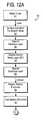
- FIG. 12A-B
- a process flow for fabricating the MIM capacitoris illustrated. Further, the process flow of the present invention can be practiced using the reactor 30 shown in FIG. 13 and/or the cluster tool 50 shown in FIG. 14 .
- the cluster tool 50 of FIG. 14is shown having two load/unload (interface) chambers 52 for the loading and unloading the wafer 51 .
- Each chamber 52can load and unload a wafer, but usual practice is to have one interface for loading and the second for unloading wafers from the tool 50 .
- cluster tool 50can be designed to accommodate one wafer or a plurality of wafers (including a cassette of wafers).
- the cluster tool 50has a number of individual cluster chambers 53 . Four are shown in the example, but the actual number will depend on the design and application.
- the interior region 54 of the toolis designed for facilitating wafer transfer between the chambers 53 clustered about, as well as to the load/unload chambers 52 .
- a handler 55(such as a robotic arm) is used to move the wafer from place to place.
- the interior area of the toolis segregated from the external environment. An inert gas or vacuum environment is typically present. It is appreciated that the operation of a generic cluster tool is known in the art.
- one chamber 56is used for M 1 layer deposition; second chamber 57 for the deposition of the sacrificial layer, as well as for its removal; third chamber 58 for the dielectric deposition; and fourth chamber 59 for the M 2 deposition.
- the waferor wafers is cleaned (block 61 ) and loaded into the first chamber 56 of the cluster tool 50 .
- Surface activation (block 62 ) of the substrate 10 , deposition of the adhesion layer 17 (block 63 ) and the deposition of the M 1 layer 11 (block 64 )are performed within chamber 56 .
- the waferis transferred to the second chamber 57 for the deposition of the sacrificial layer 12 (block 65 ) without removing the wafer from the cluster environment 54 .
- the waferis unloaded and removed to another tool for the pattern delineation to pattern the bottom electrode (block 66 ) and then etched.to form the bottom portion of the capacitor stack (block 67 ).
- the waferis reloaded into the cluster tool 60 and inserted back into the chamber 57 , where the sacrificial layer 12 is removed by a plasma etch (block 68 ).
- the waferis transferred to the third chamber 58 , where it is surface activated for dielectric deposition (block 69 ). Then the dielectric layer is deposited (block 70 ). Next the wafer is transferred to the fourth chamber 59 where it is surface activated (block 71 ) and M 2 layer deposited (block 72 ). After being unloaded from the cluster tool 50 , the wafer is again subjected to a patterning and etching to remove the excess M 2 material, so that the M 2 material resides only atop the capacitor stack (block 67 ). The final stack of M 1 dielectric-M 2 results in a MIM capacitor stack.
- the sacrificial layer 12is deposited atop the M 1 layer 11 , without subjecting the M 1 material to oxidation or contamination.
- the dielectric materialis deposited above the M 1 (after removal of the sacrificial layer) without subjecting M 1 to ambient contamination and oxidation.
- M 2is deposited over the dielectric without subjecting the dielectric layer to ambient contamination, since the wafer remains within the cluster tool between dielectric deposition and M 2 deposition. Accordingly, more pure electrode-dielectric interface(s) can be achieved for the fabrication of the MIM capacitor.
- pretreatment processesmay be used to fabricate the MIM, in that not every layer may need pretreatment to make the surface active for the ALD precursor.
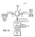
- FIG. 13An apparatus for performing ALD to practice the present invention is shown in FIG. 13 .
- An example ALD reactor apparatus 30is shown. It is appreciated reactor 30 is included within each cluster chamber 53 . Also, a variety of other devices and equipment can be utilized instead of reactor 30 .
- Reactor 30includes a processing chamber 31 for housing the wafer 51 . Typically, the wafer 51 resides atop a support (or chuck) 33 .
- a heater 34is also coupled to the chuck to heat the chuck 33 and the wafer 51 for plasma deposition.
- the processing gasesare introduced into the chamber 31 through a gas distributor 35 located at one end of the chamber 31 .
- a vacuum pump 36 and a throttling valve 37are located at the opposite end to draw and regulate the gas flow across the wafer surface.
- a mixing manifold 38is used to mix the various processing gases and the mixed gases are directed to a plasma forming zone 39 for forming the plasma.
- a variety of CVD techniques for combining gases and forming plasmacan be utilized, including adapting techniques known in the art.
- the remotely formed plasmais then fed into gas distributor 35 and then into the chamber 31 .
- the mixing manifold 38has two inlets for the introduction of chemicals.
- a carrier gasis introduced into the mixing manifold 38 .
- the carrier gasis typically an inert gas, such as nitrogen.
- the mixing manifold 38also has two inlets for other chemistries as well.
- chemical A and chemical Bare shown combined with the carrier gas.
- Chemistry Apertains to the first precursor and chemistry B pertains to the second precursor for performing ALD for the two precursor process described above.
- Chemical selection manifold 40 and 41comprised of a number of regulated valves, provide for the selection of chemicals that can be used as precursors A and B, respectively.
- Inlet valves 42 and 43respectively regulate the introduction of the precursor chemistries A and B into the mixing manifold.
- the operation of the reactor for performing ALDis as follows. Once the wafer is resident within the processing chamber 31 , the chamber environment is brought up to meet desired parameters. For example, raising the temperature of the wafer in order to perform ALD.
- the flow of carrier gasis turned on so that there is a constant regulated flow of the carrier gas as the gas is drawn by the vacuum created by the pump 36 .
- valve 42is opened to allow the first precursor to be introduced into the carrier gas flow. After a preselected time, valve 42 is closed and the carrier gas purges any remaining reactive species. Then, valve 43 is opened to introduce the second precursor into the carrier gas flow. Again after another preselected time, the valve 43 is closed and the carrier gas purges the reactive species form the chambers of the reactor.
- the two chemicals A and Bare alternately introduced into the carrier flow stream to perform the ALD cycle to deposit a film layer.
- the pretreating speciescan be introduced into the mixing manifold 38 to mix with the carrier gas. Again, the pretreatment is performed prior to the initial introduction of the first ALD precursor used to deposit the film.
- Appropriate valves 40 , 41 , 42 , 43can be activated to introduce the pretreatment chemistry into the carrier gas stream. Accordingly, the introduction of the pretreatment chemistry can be achieved from adapting designs of a standard ALD reactor.
- the present inventionprovides integration solution throughout the necessary steps of bottom electrode patterning and eliminate electrode-dielectric interface contamination.
- the integrated processcan be applied to deposit MIM structures on a variety of substrates, including BPSG, W and Wsi x .
- the bottom electrodecan be realized by a variety of metals, metal nitrides or stack of metals and/or metal nitrides.
- Ti, Ta, TaN, TiN, W/Ti, W x N/Ti, W/TiN, W x N/TiN, W/Ta, W x N/Ta, W x N/TaN, W/Al and W x N/Alcan be used.
- the dielectric selectionis comprised of a variety of high K dielectrics or stacks of high K dielectrics, including Al 2 O 3 , Ta 2 O 5 , TiO 2 , Nb 2 O 5 , HfO 2 and ZrO 2 .
- the sacrificial layercan be selected for etching by remote plasma generated fluorine.
- SiO 2 , W, W x N, Si, SiC and WSi xcan be used for the sacrificial layer.
- the top electrode material selectionis not limited by the requirement for a top layer that does not etch with fluorine. Since uniformity and conformity play less critical role for the top metal layer, other processes than ALD can be used. Accordingly, a variety of other processes may be used for the top metal layer.
Landscapes
- Chemical & Material Sciences (AREA)
- Engineering & Computer Science (AREA)
- Chemical Kinetics & Catalysis (AREA)
- General Chemical & Material Sciences (AREA)
- Mechanical Engineering (AREA)
- Materials Engineering (AREA)
- Metallurgy (AREA)
- Organic Chemistry (AREA)
- Computer Hardware Design (AREA)
- Microelectronics & Electronic Packaging (AREA)
- Power Engineering (AREA)
- Manufacturing & Machinery (AREA)
- General Physics & Mathematics (AREA)
- Condensed Matter Physics & Semiconductors (AREA)
- Physics & Mathematics (AREA)
- Chemical Vapour Deposition (AREA)
Abstract
Description
Claims (12)
Priority Applications (1)
| Application Number | Priority Date | Filing Date | Title |
|---|---|---|---|
| US09/480,804US6551399B1 (en) | 2000-01-10 | 2000-01-10 | Fully integrated process for MIM capacitors using atomic layer deposition |
Applications Claiming Priority (1)
| Application Number | Priority Date | Filing Date | Title |
|---|---|---|---|
| US09/480,804US6551399B1 (en) | 2000-01-10 | 2000-01-10 | Fully integrated process for MIM capacitors using atomic layer deposition |
Publications (1)
| Publication Number | Publication Date |
|---|---|
| US6551399B1true US6551399B1 (en) | 2003-04-22 |
Family
ID=23909425
Family Applications (1)
| Application Number | Title | Priority Date | Filing Date |
|---|---|---|---|
| US09/480,804Expired - Fee RelatedUS6551399B1 (en) | 2000-01-10 | 2000-01-10 | Fully integrated process for MIM capacitors using atomic layer deposition |
Country Status (1)
| Country | Link |
|---|---|
| US (1) | US6551399B1 (en) |
Cited By (78)
| Publication number | Priority date | Publication date | Assignee | Title |
|---|---|---|---|---|
| US20020024080A1 (en)* | 2000-08-31 | 2002-02-28 | Derderian Garo J. | Capacitor fabrication methods and capacitor constructions |
| US20020025628A1 (en)* | 2000-08-31 | 2002-02-28 | Derderian Garo J. | Capacitor fabrication methods and capacitor constructions |
| US20020076837A1 (en)* | 2000-11-30 | 2002-06-20 | Juha Hujanen | Thin films for magnetic device |
| US20020090777A1 (en)* | 2001-01-05 | 2002-07-11 | Leonard Forbes | Methods of forming capacitor structures, and capacitor structures |
| US20030013323A1 (en)* | 2001-06-14 | 2003-01-16 | Richard Hammond | Method of selective removal of SiGe alloys |
| US20030114018A1 (en)* | 2001-06-27 | 2003-06-19 | Martin Gutsche | Method for fabricating a semiconductor component |
| US20040005753A1 (en)* | 2000-05-15 | 2004-01-08 | Juhana Kostamo | Method of growing electrical conductors |
| US20040014295A1 (en)* | 2002-07-19 | 2004-01-22 | Hynix Semiconductor Inc. | Atomic layer deposition of titanium nitride using batch type chamber and method for fabricating capacitor by using the same |
| US20040026784A1 (en)* | 2002-08-08 | 2004-02-12 | O'kane William Jude | Combined atomic layer deposition and damascene processing for definition of narrow trenches |
| US20040036129A1 (en)* | 2002-08-22 | 2004-02-26 | Micron Technology, Inc. | Atomic layer deposition of CMOS gates with variable work functions |
| US20040038525A1 (en)* | 2002-08-26 | 2004-02-26 | Shuang Meng | Enhanced atomic layer deposition |
| US20040067660A1 (en)* | 2002-10-03 | 2004-04-08 | Agere Systems, Inc. | Process for semiconductor device fabrication in which a insulating layer is formed on a semiconductor substrate |
| US20040065258A1 (en)* | 2002-10-08 | 2004-04-08 | Sandhu Gurtej S. | Atomic layer deposition methods and atomic layer deposition tools |
| US20040092096A1 (en)* | 2002-10-29 | 2004-05-13 | Ivo Raaijmakers | Oxygen bridge structures and methods to form oxygen bridge structures |
| US20040121620A1 (en)* | 2000-11-24 | 2004-06-24 | Pomarede Christophe F. | Surface preparation prior to deposition |
| US6759081B2 (en) | 2001-05-11 | 2004-07-06 | Asm International, N.V. | Method of depositing thin films for magnetic heads |
| US6818517B1 (en)* | 2003-08-29 | 2004-11-16 | Asm International N.V. | Methods of depositing two or more layers on a substrate in situ |
| EP1480257A1 (en)* | 2003-05-20 | 2004-11-24 | STMicroelectronics S.A. | Method of manufacturing an electronic integrated circuit having a capacitor |
| US20050018381A1 (en)* | 2003-07-21 | 2005-01-27 | Mcclure Brent A. | Capacitor constructions and methods of forming |
| US20050051824A1 (en)* | 2001-06-13 | 2005-03-10 | Toshihiro Iizuka | Semiconductor device having a thin film capacitor and method for fabricating the same |
| US20050079669A1 (en)* | 2002-01-24 | 2005-04-14 | Infineon Technologies Ag | Method of producing a capacitor in a dielectric layer |
| US20060063346A1 (en)* | 2004-06-10 | 2006-03-23 | Jong-Cheol Lee | Method of forming a layer and method of forming a capacitor of a semiconductor device having the same |
| US20060151852A1 (en)* | 2002-07-19 | 2006-07-13 | Yoshihide Senzaki | In-situ formation of metal insulator metal capacitors cross reference to related applications |
| US7097878B1 (en) | 2004-06-22 | 2006-08-29 | Novellus Systems, Inc. | Mixed alkoxy precursors and methods of their use for rapid vapor deposition of SiO2 films |
| US7112503B1 (en)* | 2000-08-31 | 2006-09-26 | Micron Technology, Inc. | Enhanced surface area capacitor fabrication methods |
| US7148155B1 (en) | 2004-10-26 | 2006-12-12 | Novellus Systems, Inc. | Sequential deposition/anneal film densification method |
| US20060290013A1 (en)* | 2005-06-27 | 2006-12-28 | Ya-Hong Xie | Method for chemical vapor deposition in high aspect ratio spaces |
| KR100663341B1 (en)* | 2000-08-11 | 2007-01-02 | 삼성전자주식회사 | Atomic Layer Deposition Capacitor Manufacturing Method and Apparatus |
| US20070014919A1 (en)* | 2005-07-15 | 2007-01-18 | Jani Hamalainen | Atomic layer deposition of noble metal oxides |
| US20070018244A1 (en)* | 2005-07-20 | 2007-01-25 | Applied Materials, Inc. | Gate Electrode structures and methods of manufacture |
| US20070026654A1 (en)* | 2005-03-15 | 2007-02-01 | Hannu Huotari | Systems and methods for avoiding base address collisions |
| US20070036892A1 (en)* | 2005-03-15 | 2007-02-15 | Haukka Suvi P | Enhanced deposition of noble metals |
| US20070082470A1 (en)* | 2000-08-07 | 2007-04-12 | Amberwave System Corporation | Gate technology for strained surface channel and strained buried channel MOSFET devices |
| US20070202694A1 (en)* | 2005-10-31 | 2007-08-30 | Jung-Hun Seo | Method of forming a layer and method of removing reaction by-products |
| US20070234949A1 (en)* | 2006-04-07 | 2007-10-11 | Micron Technology, Inc. | Atomic layer deposited titanium-doped indium oxide films |
| US7288463B1 (en) | 2006-04-28 | 2007-10-30 | Novellus Systems, Inc. | Pulsed deposition layer gap fill with expansion material |
| US7294583B1 (en) | 2004-12-23 | 2007-11-13 | Novellus Systems, Inc. | Methods for the use of alkoxysilanol precursors for vapor deposition of SiO2 films |
| US20080081114A1 (en)* | 2006-10-03 | 2008-04-03 | Novellus Systems, Inc. | Apparatus and method for delivering uniform fluid flow in a chemical deposition system |
| US20080105901A1 (en)* | 2006-11-07 | 2008-05-08 | Kamal Tabatabaie | Atomic layer deposition in the formation of gate structures for iii-v semiconductor |
| US20080124484A1 (en)* | 2006-11-08 | 2008-05-29 | Asm Japan K.K. | Method of forming ru film and metal wiring structure |
| US20080318417A1 (en)* | 2006-09-01 | 2008-12-25 | Asm Japan K.K. | Method of forming ruthenium film for metal wiring structure |
| US7482247B1 (en) | 2004-12-30 | 2009-01-27 | Novellus Systems, Inc. | Conformal nanolaminate dielectric deposition and etch bag gap fill process |
| US7491653B1 (en) | 2005-12-23 | 2009-02-17 | Novellus Systems, Inc. | Metal-free catalysts for pulsed deposition layer process for conformal silica laminates |
| US20090087339A1 (en)* | 2007-09-28 | 2009-04-02 | Asm Japan K.K. | METHOD FOR FORMING RUTHENIUM COMPLEX FILM USING Beta-DIKETONE-COORDINATED RUTHENIUM PRECURSOR |
| US20090149008A1 (en)* | 2007-10-05 | 2009-06-11 | Applied Materials, Inc. | Method for depositing group iii/v compounds |
| US20090155997A1 (en)* | 2007-12-12 | 2009-06-18 | Asm Japan K.K. | METHOD FOR FORMING Ta-Ru LINER LAYER FOR Cu WIRING |
| US20090163024A1 (en)* | 2007-12-21 | 2009-06-25 | Asm Genitech Korea Ltd. | Methods of depositing a ruthenium film |
| US20090209101A1 (en)* | 2008-02-19 | 2009-08-20 | Asm Japan K.K. | Ruthenium alloy film for copper interconnects |
| US7589028B1 (en) | 2005-11-15 | 2009-09-15 | Novellus Systems, Inc. | Hydroxyl bond removal and film densification method for oxide films using microwave post treatment |
| US7625820B1 (en) | 2006-06-21 | 2009-12-01 | Novellus Systems, Inc. | Method of selective coverage of high aspect ratio structures with a conformal film |
| US20100055433A1 (en)* | 2008-08-29 | 2010-03-04 | Asm Japan K.K. | Atomic composition controlled ruthenium alloy film formed by plasma-enhanced atomic layer deposition |
| US7709402B2 (en) | 2006-02-16 | 2010-05-04 | Micron Technology, Inc. | Conductive layers for hafnium silicon oxynitride films |
| US20100112813A1 (en)* | 2008-11-06 | 2010-05-06 | Akihiro Takase | Manufacturing method for semiconductor device |
| US7737035B1 (en) | 2006-03-31 | 2010-06-15 | Novellus Systems, Inc. | Dual seal deposition process chamber and process |
| US20100215854A1 (en)* | 2007-06-24 | 2010-08-26 | Burrows Brian H | Hvpe showerhead design |
| US7790633B1 (en) | 2004-10-26 | 2010-09-07 | Novellus Systems, Inc. | Sequential deposition/anneal film densification method |
| US20100258052A1 (en)* | 2009-04-10 | 2010-10-14 | Applied Materials, Inc. | Hvpe precursor source hardware |
| US20100261340A1 (en)* | 2009-04-10 | 2010-10-14 | Applied Materials, Inc. | Cluster tool for leds |
| US20100273318A1 (en)* | 2009-04-24 | 2010-10-28 | Applied Materials, Inc. | Substrate pretreatment for subsequent high temperature group iii depositions |
| US20100273290A1 (en)* | 2009-04-28 | 2010-10-28 | Applied Materials, Inc. | Mocvd single chamber split process for led manufacturing |
| US20100279020A1 (en)* | 2009-04-29 | 2010-11-04 | Applied Materials, Inc. | METHOD OF FORMING IN-SITU PRE-GaN DEPOSITION LAYER IN HVPE |
| US20110020546A1 (en)* | 2009-05-15 | 2011-01-27 | Asm International N.V. | Low Temperature ALD of Noble Metals |
| US20110027977A1 (en)* | 2009-07-31 | 2011-02-03 | Asm America, Inc. | Deposition of ruthenium or ruthenium dioxide |
| US7993457B1 (en) | 2007-01-23 | 2011-08-09 | Novellus Systems, Inc. | Deposition sub-chamber with variable flow |
| US8133555B2 (en) | 2008-10-14 | 2012-03-13 | Asm Japan K.K. | Method for forming metal film by ALD using beta-diketone metal complex |
| US20120178256A1 (en)* | 2001-02-02 | 2012-07-12 | Seutter Sean M | Formation of a tantalum-nitride layer |
| US8273408B2 (en) | 2007-10-17 | 2012-09-25 | Asm Genitech Korea Ltd. | Methods of depositing a ruthenium film |
| US8361892B2 (en) | 2010-04-14 | 2013-01-29 | Applied Materials, Inc. | Multiple precursor showerhead with by-pass ports |
| US8633110B2 (en) | 2005-07-20 | 2014-01-21 | Micron Technology, Inc. | Titanium nitride films |
| US9057128B2 (en) | 2011-03-18 | 2015-06-16 | Applied Materials, Inc. | Multiple level showerhead design |
| US9129897B2 (en) | 2008-12-19 | 2015-09-08 | Asm International N.V. | Metal silicide, metal germanide, methods for making the same |
| US9353439B2 (en) | 2013-04-05 | 2016-05-31 | Lam Research Corporation | Cascade design showerhead for transient uniformity |
| US9379011B2 (en) | 2008-12-19 | 2016-06-28 | Asm International N.V. | Methods for depositing nickel films and for making nickel silicide and nickel germanide |
| US9607842B1 (en) | 2015-10-02 | 2017-03-28 | Asm Ip Holding B.V. | Methods of forming metal silicides |
| US10023959B2 (en) | 2015-05-26 | 2018-07-17 | Lam Research Corporation | Anti-transient showerhead |
| US20190112709A1 (en)* | 2017-10-12 | 2019-04-18 | Gelest Technologies, Inc. | Methods and System for the Integrated Synthesis, Delivery, and Processing of Source Chemicals for Thin Film Manufacturing |
| US20200135552A1 (en)* | 2018-10-31 | 2020-04-30 | Taiwan Semiconductor Manufacturing Co., Ltd. | High breakdown voltage inter-metal dielectric layer |
| US12354877B2 (en) | 2020-06-24 | 2025-07-08 | Asm Ip Holding B.V. | Vapor deposition of films comprising molybdenum |
Citations (61)
| Publication number | Priority date | Publication date | Assignee | Title |
|---|---|---|---|---|
| US4058430A (en) | 1974-11-29 | 1977-11-15 | Tuomo Suntola | Method for producing compound thin films |
| US4389973A (en) | 1980-03-18 | 1983-06-28 | Oy Lohja Ab | Apparatus for performing growth of compound thin films |
| US4413022A (en) | 1979-02-28 | 1983-11-01 | Canon Kabushiki Kaisha | Method for performing growth of compound thin films |
| US4416933A (en) | 1981-02-23 | 1983-11-22 | Oy Lohja Ab | Thin film electroluminescence structure |
| JPS6010625A (en) | 1983-06-29 | 1985-01-19 | Tokyo Denshi Kagaku Kabushiki | Multistage plasma processor |
| US4533410A (en) | 1982-10-19 | 1985-08-06 | Matsushita Electric Industrial Co., Ltd. | Process of vapor phase epitaxy of compound semiconductors |
| US4533820A (en) | 1982-06-25 | 1985-08-06 | Ushio Denki Kabushiki Kaisha | Radiant heating apparatus |
| US4689247A (en) | 1986-05-15 | 1987-08-25 | Ametek, Inc. | Process and apparatus for forming thin films |
| US4828224A (en) | 1987-10-15 | 1989-05-09 | Epsilon Technology, Inc. | Chemical vapor deposition system |
| US4836138A (en) | 1987-06-18 | 1989-06-06 | Epsilon Technology, Inc. | Heating system for reaction chamber of chemical vapor deposition equipment |
| US4846102A (en) | 1987-06-24 | 1989-07-11 | Epsilon Technology, Inc. | Reaction chambers for CVD systems |
| US4907862A (en) | 1985-03-05 | 1990-03-13 | Oy Lohja Ab | Method for generating elecronically controllable color elements and color display based on the method |
| US4913929A (en) | 1987-04-21 | 1990-04-03 | The Board Of Trustees Of The Leland Stanford Junior University | Thermal/microwave remote plasma multiprocessing reactor and method of use |
| JPH02152251A (en) | 1988-12-03 | 1990-06-12 | Furendotetsuku Kenkyusho:Kk | Manufacturing system of vertical-type semiconductor |
| US4975252A (en) | 1984-07-26 | 1990-12-04 | Junichi Nishizawa | Semiconductor crystal growth apparatus |
| US4976996A (en) | 1987-02-17 | 1990-12-11 | Lam Research Corporation | Chemical vapor deposition reactor and method of use thereof |
| US4993360A (en) | 1988-03-28 | 1991-02-19 | Kabushiki Kaisha Toshiba | Vapor growth apparatus having a diffuser section containing a flow regulating member |
| US5000113A (en) | 1986-12-19 | 1991-03-19 | Applied Materials, Inc. | Thermal CVD/PECVD reactor and use for thermal chemical vapor deposition of silicon dioxide and in-situ multi-step planarized process |
| US5015503A (en) | 1990-02-07 | 1991-05-14 | The University Of Delaware | Apparatus for producing compound semiconductor thin films |
| WO1991010510A1 (en) | 1990-01-16 | 1991-07-25 | Neste Oy | Process and apparatus for preparing heterogeneous catalysts |
| EP0442490A1 (en) | 1990-02-14 | 1991-08-21 | Sumitomo Electric Industries, Ltd. | Method for producing single crystal boron nitride film |
| US5072262A (en)* | 1986-03-11 | 1991-12-10 | Kanegafuchi Kagaku Kogyo Kabushiki Kaisha | Electric-electronic device including polyimide thin film |
| US5071733A (en)* | 1986-05-20 | 1991-12-10 | Kanegafuchi Kagaku Kogyo Kabushiki Kaisha | Patterned thin film and process for preparing the same |
| US5078851A (en) | 1989-07-26 | 1992-01-07 | Kouji Nishihata | Low-temperature plasma processor |
| US5077875A (en) | 1990-01-31 | 1992-01-07 | Raytheon Company | Reactor vessel for the growth of heterojunction devices |
| US5119760A (en) | 1988-12-27 | 1992-06-09 | Symetrix Corporation | Methods and apparatus for material deposition |
| US5156820A (en) | 1989-05-15 | 1992-10-20 | Rapro Technology, Inc. | Reaction chamber with controlled radiant energy heating and distributed reactant flow |
| US5194401A (en) | 1989-04-18 | 1993-03-16 | Applied Materials, Inc. | Thermally processing semiconductor wafers at non-ambient pressures |
| US5204314A (en) | 1990-07-06 | 1993-04-20 | Advanced Technology Materials, Inc. | Method for delivering an involatile reagent in vapor form to a CVD reactor |
| JPH05152215A (en) | 1991-11-29 | 1993-06-18 | Hitachi Ltd | Film formation device |
| US5270247A (en) | 1991-07-12 | 1993-12-14 | Fujitsu Limited | Atomic layer epitaxy of compound semiconductor |
| US5281274A (en) | 1990-06-22 | 1994-01-25 | The United States Of America As Represented By The Secretary Of The Navy | Atomic layer epitaxy (ALE) apparatus for growing thin films of elemental semiconductors |
| US5294778A (en) | 1991-09-11 | 1994-03-15 | Lam Research Corporation | CVD platen heater system utilizing concentric electric heating elements |
| US5320680A (en) | 1991-04-25 | 1994-06-14 | Silicon Valley Group, Inc. | Primary flow CVD apparatus comprising gas preheater and means for substantially eddy-free gas flow |
| US5336327A (en) | 1992-06-01 | 1994-08-09 | Motorola, Inc. | CVD reactor with uniform layer depositing ability |
| US5484484A (en) | 1993-07-03 | 1996-01-16 | Tokyo Electron Kabushiki | Thermal processing method and apparatus therefor |
| US5552910A (en)* | 1993-11-29 | 1996-09-03 | Sharp Kabushiki Kaisha | Liquid crystal display having zinc sulfide switching elements and method for producing the same |
| JPH08236459A (en) | 1995-02-27 | 1996-09-13 | Sony Corp | Cvd device |
| US5582866A (en) | 1993-01-28 | 1996-12-10 | Applied Materials, Inc. | Single substrate vacuum processing apparatus having improved exhaust system |
| US5693139A (en) | 1984-07-26 | 1997-12-02 | Research Development Corporation Of Japan | Growth of doped semiconductor monolayers |
| US5711811A (en) | 1994-11-28 | 1998-01-27 | Mikrokemia Oy | Method and equipment for growing thin films |
| US5716709A (en)* | 1994-07-14 | 1998-02-10 | Competitive Technologies, Inc. | Multilayered nanostructures comprising alternating organic and inorganic ionic layers |
| JPH10102256A (en) | 1996-09-14 | 1998-04-21 | Samsung Electron Co Ltd | CVD equipment |
| US5749974A (en) | 1994-07-15 | 1998-05-12 | Shin-Etsu Handotai Co., Ltd. | Method of chemical vapor deposition and reactor therefor |
| US5788447A (en) | 1995-08-05 | 1998-08-04 | Kokusai Electric Co., Ltd. | Substrate processing apparatus |
| US5851849A (en) | 1997-05-22 | 1998-12-22 | Lucent Technologies Inc. | Process for passivating semiconductor laser structures with severe steps in surface topography |
| US5879459A (en) | 1997-08-29 | 1999-03-09 | Genus, Inc. | Vertically-stacked process reactor and cluster tool system for atomic layer deposition |
| US5916365A (en) | 1996-08-16 | 1999-06-29 | Sherman; Arthur | Sequential chemical vapor deposition |
| US5935338A (en) | 1993-04-05 | 1999-08-10 | Applied Materials, Inc. | Chemical vapor deposition chamber |
| US6007330A (en) | 1998-03-12 | 1999-12-28 | Cosmos Factory, Inc. | Liquid precursor delivery system |
| US6015590A (en) | 1994-11-28 | 2000-01-18 | Neste Oy | Method for growing thin films |
| US6042652A (en) | 1999-05-01 | 2000-03-28 | P.K. Ltd | Atomic layer deposition apparatus for depositing atomic layer on multiple substrates |
| US6050216A (en) | 1998-08-21 | 2000-04-18 | M.E.C. Technology, Inc. | Showerhead electrode for plasma processing |
| US6077775A (en) | 1998-08-20 | 2000-06-20 | The United States Of America As Represented By The Secretary Of The Navy | Process for making a semiconductor device with barrier film formation using a metal halide and products thereof |
| US6090442A (en) | 1997-04-14 | 2000-07-18 | University Technology Corporation | Method of growing films on substrates at room temperatures using catalyzed binary reaction sequence chemistry |
| US6124158A (en) | 1999-06-08 | 2000-09-26 | Lucent Technologies Inc. | Method of reducing carbon contamination of a thin dielectric film by using gaseous organic precursors, inert gas, and ozone to react with carbon contaminants |
| US6139700A (en) | 1997-10-01 | 2000-10-31 | Samsung Electronics Co., Ltd. | Method of and apparatus for forming a metal interconnection in the contact hole of a semiconductor device |
| US6143659A (en) | 1997-11-18 | 2000-11-07 | Samsung Electronics, Co., Ltd. | Method for manufacturing aluminum metal interconnection layer by atomic layer deposition method |
| US6200893B1 (en) | 1999-03-11 | 2001-03-13 | Genus, Inc | Radical-assisted sequential CVD |
| US6270572B1 (en) | 1998-08-07 | 2001-08-07 | Samsung Electronics Co., Ltd. | Method for manufacturing thin film using atomic layer deposition |
| US6305314B1 (en) | 1999-03-11 | 2001-10-23 | Genvs, Inc. | Apparatus and concept for minimizing parasitic chemical vapor deposition during atomic layer deposition |
- 2000
- 2000-01-10USUS09/480,804patent/US6551399B1/ennot_activeExpired - Fee Related
Patent Citations (62)
| Publication number | Priority date | Publication date | Assignee | Title |
|---|---|---|---|---|
| US4058430A (en) | 1974-11-29 | 1977-11-15 | Tuomo Suntola | Method for producing compound thin films |
| US4413022A (en) | 1979-02-28 | 1983-11-01 | Canon Kabushiki Kaisha | Method for performing growth of compound thin films |
| US4389973A (en) | 1980-03-18 | 1983-06-28 | Oy Lohja Ab | Apparatus for performing growth of compound thin films |
| US4416933A (en) | 1981-02-23 | 1983-11-22 | Oy Lohja Ab | Thin film electroluminescence structure |
| US4533820A (en) | 1982-06-25 | 1985-08-06 | Ushio Denki Kabushiki Kaisha | Radiant heating apparatus |
| US4533410A (en) | 1982-10-19 | 1985-08-06 | Matsushita Electric Industrial Co., Ltd. | Process of vapor phase epitaxy of compound semiconductors |
| JPS6010625A (en) | 1983-06-29 | 1985-01-19 | Tokyo Denshi Kagaku Kabushiki | Multistage plasma processor |
| US5693139A (en) | 1984-07-26 | 1997-12-02 | Research Development Corporation Of Japan | Growth of doped semiconductor monolayers |
| US4975252A (en) | 1984-07-26 | 1990-12-04 | Junichi Nishizawa | Semiconductor crystal growth apparatus |
| US4907862A (en) | 1985-03-05 | 1990-03-13 | Oy Lohja Ab | Method for generating elecronically controllable color elements and color display based on the method |
| US5072262A (en)* | 1986-03-11 | 1991-12-10 | Kanegafuchi Kagaku Kogyo Kabushiki Kaisha | Electric-electronic device including polyimide thin film |
| US4689247A (en) | 1986-05-15 | 1987-08-25 | Ametek, Inc. | Process and apparatus for forming thin films |
| US5071733A (en)* | 1986-05-20 | 1991-12-10 | Kanegafuchi Kagaku Kogyo Kabushiki Kaisha | Patterned thin film and process for preparing the same |
| US5000113A (en) | 1986-12-19 | 1991-03-19 | Applied Materials, Inc. | Thermal CVD/PECVD reactor and use for thermal chemical vapor deposition of silicon dioxide and in-situ multi-step planarized process |
| US4976996A (en) | 1987-02-17 | 1990-12-11 | Lam Research Corporation | Chemical vapor deposition reactor and method of use thereof |
| US4913929A (en) | 1987-04-21 | 1990-04-03 | The Board Of Trustees Of The Leland Stanford Junior University | Thermal/microwave remote plasma multiprocessing reactor and method of use |
| US4836138A (en) | 1987-06-18 | 1989-06-06 | Epsilon Technology, Inc. | Heating system for reaction chamber of chemical vapor deposition equipment |
| US4846102A (en) | 1987-06-24 | 1989-07-11 | Epsilon Technology, Inc. | Reaction chambers for CVD systems |
| US4828224A (en) | 1987-10-15 | 1989-05-09 | Epsilon Technology, Inc. | Chemical vapor deposition system |
| US4993360A (en) | 1988-03-28 | 1991-02-19 | Kabushiki Kaisha Toshiba | Vapor growth apparatus having a diffuser section containing a flow regulating member |
| JPH02152251A (en) | 1988-12-03 | 1990-06-12 | Furendotetsuku Kenkyusho:Kk | Manufacturing system of vertical-type semiconductor |
| US5119760A (en) | 1988-12-27 | 1992-06-09 | Symetrix Corporation | Methods and apparatus for material deposition |
| US5194401A (en) | 1989-04-18 | 1993-03-16 | Applied Materials, Inc. | Thermally processing semiconductor wafers at non-ambient pressures |
| US5156820A (en) | 1989-05-15 | 1992-10-20 | Rapro Technology, Inc. | Reaction chamber with controlled radiant energy heating and distributed reactant flow |
| US5078851A (en) | 1989-07-26 | 1992-01-07 | Kouji Nishihata | Low-temperature plasma processor |
| EP0511264A1 (en) | 1990-01-16 | 1992-11-04 | Neste Oy | Process and apparatus for preparing heterogeneous catalysts. |
| WO1991010510A1 (en) | 1990-01-16 | 1991-07-25 | Neste Oy | Process and apparatus for preparing heterogeneous catalysts |
| US5077875A (en) | 1990-01-31 | 1992-01-07 | Raytheon Company | Reactor vessel for the growth of heterojunction devices |
| US5015503A (en) | 1990-02-07 | 1991-05-14 | The University Of Delaware | Apparatus for producing compound semiconductor thin films |
| EP0442490A1 (en) | 1990-02-14 | 1991-08-21 | Sumitomo Electric Industries, Ltd. | Method for producing single crystal boron nitride film |
| US5281274A (en) | 1990-06-22 | 1994-01-25 | The United States Of America As Represented By The Secretary Of The Navy | Atomic layer epitaxy (ALE) apparatus for growing thin films of elemental semiconductors |
| US5204314A (en) | 1990-07-06 | 1993-04-20 | Advanced Technology Materials, Inc. | Method for delivering an involatile reagent in vapor form to a CVD reactor |
| US5320680A (en) | 1991-04-25 | 1994-06-14 | Silicon Valley Group, Inc. | Primary flow CVD apparatus comprising gas preheater and means for substantially eddy-free gas flow |
| US5270247A (en) | 1991-07-12 | 1993-12-14 | Fujitsu Limited | Atomic layer epitaxy of compound semiconductor |
| US5294778A (en) | 1991-09-11 | 1994-03-15 | Lam Research Corporation | CVD platen heater system utilizing concentric electric heating elements |
| JPH05152215A (en) | 1991-11-29 | 1993-06-18 | Hitachi Ltd | Film formation device |
| US5336327A (en) | 1992-06-01 | 1994-08-09 | Motorola, Inc. | CVD reactor with uniform layer depositing ability |
| US5582866A (en) | 1993-01-28 | 1996-12-10 | Applied Materials, Inc. | Single substrate vacuum processing apparatus having improved exhaust system |
| US5935338A (en) | 1993-04-05 | 1999-08-10 | Applied Materials, Inc. | Chemical vapor deposition chamber |
| US5484484A (en) | 1993-07-03 | 1996-01-16 | Tokyo Electron Kabushiki | Thermal processing method and apparatus therefor |
| US5552910A (en)* | 1993-11-29 | 1996-09-03 | Sharp Kabushiki Kaisha | Liquid crystal display having zinc sulfide switching elements and method for producing the same |
| US5716709A (en)* | 1994-07-14 | 1998-02-10 | Competitive Technologies, Inc. | Multilayered nanostructures comprising alternating organic and inorganic ionic layers |
| US5749974A (en) | 1994-07-15 | 1998-05-12 | Shin-Etsu Handotai Co., Ltd. | Method of chemical vapor deposition and reactor therefor |
| US5711811A (en) | 1994-11-28 | 1998-01-27 | Mikrokemia Oy | Method and equipment for growing thin films |
| US6015590A (en) | 1994-11-28 | 2000-01-18 | Neste Oy | Method for growing thin films |
| JPH08236459A (en) | 1995-02-27 | 1996-09-13 | Sony Corp | Cvd device |
| US5788447A (en) | 1995-08-05 | 1998-08-04 | Kokusai Electric Co., Ltd. | Substrate processing apparatus |
| US5916365A (en) | 1996-08-16 | 1999-06-29 | Sherman; Arthur | Sequential chemical vapor deposition |
| JPH10102256A (en) | 1996-09-14 | 1998-04-21 | Samsung Electron Co Ltd | CVD equipment |
| US6090442A (en) | 1997-04-14 | 2000-07-18 | University Technology Corporation | Method of growing films on substrates at room temperatures using catalyzed binary reaction sequence chemistry |
| US5851849A (en) | 1997-05-22 | 1998-12-22 | Lucent Technologies Inc. | Process for passivating semiconductor laser structures with severe steps in surface topography |
| US5879459A (en) | 1997-08-29 | 1999-03-09 | Genus, Inc. | Vertically-stacked process reactor and cluster tool system for atomic layer deposition |
| US6139700A (en) | 1997-10-01 | 2000-10-31 | Samsung Electronics Co., Ltd. | Method of and apparatus for forming a metal interconnection in the contact hole of a semiconductor device |
| US6143659A (en) | 1997-11-18 | 2000-11-07 | Samsung Electronics, Co., Ltd. | Method for manufacturing aluminum metal interconnection layer by atomic layer deposition method |
| US6007330A (en) | 1998-03-12 | 1999-12-28 | Cosmos Factory, Inc. | Liquid precursor delivery system |
| US6270572B1 (en) | 1998-08-07 | 2001-08-07 | Samsung Electronics Co., Ltd. | Method for manufacturing thin film using atomic layer deposition |
| US6077775A (en) | 1998-08-20 | 2000-06-20 | The United States Of America As Represented By The Secretary Of The Navy | Process for making a semiconductor device with barrier film formation using a metal halide and products thereof |
| US6050216A (en) | 1998-08-21 | 2000-04-18 | M.E.C. Technology, Inc. | Showerhead electrode for plasma processing |
| US6200893B1 (en) | 1999-03-11 | 2001-03-13 | Genus, Inc | Radical-assisted sequential CVD |
| US6305314B1 (en) | 1999-03-11 | 2001-10-23 | Genvs, Inc. | Apparatus and concept for minimizing parasitic chemical vapor deposition during atomic layer deposition |
| US6042652A (en) | 1999-05-01 | 2000-03-28 | P.K. Ltd | Atomic layer deposition apparatus for depositing atomic layer on multiple substrates |
| US6124158A (en) | 1999-06-08 | 2000-09-26 | Lucent Technologies Inc. | Method of reducing carbon contamination of a thin dielectric film by using gaseous organic precursors, inert gas, and ozone to react with carbon contaminants |
Non-Patent Citations (121)
Cited By (168)
| Publication number | Priority date | Publication date | Assignee | Title |
|---|---|---|---|---|
| US20040005753A1 (en)* | 2000-05-15 | 2004-01-08 | Juhana Kostamo | Method of growing electrical conductors |
| US8536058B2 (en) | 2000-05-15 | 2013-09-17 | Asm International N.V. | Method of growing electrical conductors |
| US7955979B2 (en) | 2000-05-15 | 2011-06-07 | Asm International N.V. | Method of growing electrical conductors |
| US7494927B2 (en) | 2000-05-15 | 2009-02-24 | Asm International N.V. | Method of growing electrical conductors |
| US20080146042A1 (en)* | 2000-05-15 | 2008-06-19 | Asm International N.V. | Method of growing electrical conductors |
| US20070082470A1 (en)* | 2000-08-07 | 2007-04-12 | Amberwave System Corporation | Gate technology for strained surface channel and strained buried channel MOSFET devices |
| KR100663341B1 (en)* | 2000-08-11 | 2007-01-02 | 삼성전자주식회사 | Atomic Layer Deposition Capacitor Manufacturing Method and Apparatus |
| US20070178640A1 (en)* | 2000-08-31 | 2007-08-02 | Derderian Garo J | Capacitor fabrication methods and capacitor constructions |
| US20020024080A1 (en)* | 2000-08-31 | 2002-02-28 | Derderian Garo J. | Capacitor fabrication methods and capacitor constructions |
| US7112503B1 (en)* | 2000-08-31 | 2006-09-26 | Micron Technology, Inc. | Enhanced surface area capacitor fabrication methods |
| US7109542B2 (en) | 2000-08-31 | 2006-09-19 | Micron Technology, Inc. | Capacitor constructions having a conductive layer |
| US7053432B2 (en) | 2000-08-31 | 2006-05-30 | Micron Technology, Inc. | Enhanced surface area capacitor fabrication methods |
| US20070007572A1 (en)* | 2000-08-31 | 2007-01-11 | Agarwal Vishnu K | Capacitor fabrication methods and capacitor constructions |
| US7217615B1 (en) | 2000-08-31 | 2007-05-15 | Micron Technology, Inc. | Capacitor fabrication methods including forming a conductive layer |
| US20020025628A1 (en)* | 2000-08-31 | 2002-02-28 | Derderian Garo J. | Capacitor fabrication methods and capacitor constructions |
| US20040147101A1 (en)* | 2000-11-24 | 2004-07-29 | Pomarede Christophe F. | Surface preparation prior to deposition |
| US7056835B2 (en)* | 2000-11-24 | 2006-06-06 | Asm America, Inc. | Surface preparation prior to deposition |
| US20040121620A1 (en)* | 2000-11-24 | 2004-06-24 | Pomarede Christophe F. | Surface preparation prior to deposition |
| US7476627B2 (en) | 2000-11-24 | 2009-01-13 | Asm America, Inc. | Surface preparation prior to deposition |
| US20060205230A1 (en)* | 2000-11-24 | 2006-09-14 | Pomarede Christophe F | Surface preparation prior to deposition |
| US6958277B2 (en) | 2000-11-24 | 2005-10-25 | Asm America, Inc. | Surface preparation prior to deposition |
| US7220669B2 (en)* | 2000-11-30 | 2007-05-22 | Asm International N.V. | Thin films for magnetic device |
| US20020076837A1 (en)* | 2000-11-30 | 2002-06-20 | Juha Hujanen | Thin films for magnetic device |
| US20020090777A1 (en)* | 2001-01-05 | 2002-07-11 | Leonard Forbes | Methods of forming capacitor structures, and capacitor structures |
| US7166883B2 (en)* | 2001-01-05 | 2007-01-23 | Micron Technology, Inc. | Capacitor structures |
| US7192827B2 (en) | 2001-01-05 | 2007-03-20 | Micron Technology, Inc. | Methods of forming capacitor structures |
| US20050167723A1 (en)* | 2001-01-05 | 2005-08-04 | Leonard Forbes | Capacitor structures |
| US20050026355A1 (en)* | 2001-01-05 | 2005-02-03 | Leonard Forbes | Capacitor structures |
| US20020164852A1 (en)* | 2001-01-05 | 2002-11-07 | Leonard Forbes | Capacitor structures |
| US9012334B2 (en)* | 2001-02-02 | 2015-04-21 | Applied Materials, Inc. | Formation of a tantalum-nitride layer |
| US20120178256A1 (en)* | 2001-02-02 | 2012-07-12 | Seutter Sean M | Formation of a tantalum-nitride layer |
| US6759081B2 (en) | 2001-05-11 | 2004-07-06 | Asm International, N.V. | Method of depositing thin films for magnetic heads |
| US20040161636A1 (en)* | 2001-05-11 | 2004-08-19 | Juha Hujanen | Method of depositing thin films for magnetic heads |
| US20050051824A1 (en)* | 2001-06-13 | 2005-03-10 | Toshihiro Iizuka | Semiconductor device having a thin film capacitor and method for fabricating the same |
| US8815678B2 (en) | 2001-06-13 | 2014-08-26 | Renesas Electronics Corporation | Method for fabricating a metal-insulator-metal (MIM) capacitor having capacitor dielectric layer formed by atomic layer deposition (ALD) |
| US20070152256A1 (en)* | 2001-06-13 | 2007-07-05 | Toshihiro Iizuka | Method for fabricating a metal insulator-metal (MIM) capacitor having capacitor dielectric layer formed by atomic layer deposition (ALD) |
| US8169013B2 (en) | 2001-06-13 | 2012-05-01 | Renesas Electronics Corporation | Metal-insulator-metal (MIM) capacitor having capacitor dielectric material selected from a group consisting of ZRO2, HFO2, (ZRX, HF1-X)O2 (0<x<1), (ZRy, Ti (O<y<1), (Hfz, Ti-z)O2 (O<z<1) and (Zrk, Ti1, Hfm)O2 (O<K, 1, m<1, K+1+m=1) |
| US20030013323A1 (en)* | 2001-06-14 | 2003-01-16 | Richard Hammond | Method of selective removal of SiGe alloys |
| US20040171223A1 (en)* | 2001-06-14 | 2004-09-02 | Amberwave Systems Corporation | Method of selective removal of SiGe alloys |
| US20030114018A1 (en)* | 2001-06-27 | 2003-06-19 | Martin Gutsche | Method for fabricating a semiconductor component |
| US20050079669A1 (en)* | 2002-01-24 | 2005-04-14 | Infineon Technologies Ag | Method of producing a capacitor in a dielectric layer |
| US7132346B2 (en)* | 2002-07-19 | 2006-11-07 | Hynix Semiconductor Inc. | Atomic layer deposition of titanium using batch type chamber and method for fabricating capacitor by using the same |
| US7335569B2 (en)* | 2002-07-19 | 2008-02-26 | Aviza Technology, Inc. | In-situ formation of metal insulator metal capacitors |
| US20060151852A1 (en)* | 2002-07-19 | 2006-07-13 | Yoshihide Senzaki | In-situ formation of metal insulator metal capacitors cross reference to related applications |
| US20060040461A1 (en)* | 2002-07-19 | 2006-02-23 | Hynix Semiconductor Inc. | Method of forming a capacitor |
| US20040014295A1 (en)* | 2002-07-19 | 2004-01-22 | Hynix Semiconductor Inc. | Atomic layer deposition of titanium nitride using batch type chamber and method for fabricating capacitor by using the same |
| US6949833B2 (en) | 2002-08-08 | 2005-09-27 | Seagate Technology Llc | Combined atomic layer deposition and damascene processing for definition of narrow trenches |
| US20040026784A1 (en)* | 2002-08-08 | 2004-02-12 | O'kane William Jude | Combined atomic layer deposition and damascene processing for definition of narrow trenches |
| US20040036129A1 (en)* | 2002-08-22 | 2004-02-26 | Micron Technology, Inc. | Atomic layer deposition of CMOS gates with variable work functions |
| US7279732B2 (en) | 2002-08-26 | 2007-10-09 | Micron Technology, Inc. | Enhanced atomic layer deposition |
| US20080251828A1 (en)* | 2002-08-26 | 2008-10-16 | Micron Technology, Inc. | Enhanced atomic layer deposition |
| US6967154B2 (en)* | 2002-08-26 | 2005-11-22 | Micron Technology, Inc. | Enhanced atomic layer deposition |
| US20040217410A1 (en)* | 2002-08-26 | 2004-11-04 | Micron Technology, Inc. | Enhanced atomic layer deposition |
| US20040038525A1 (en)* | 2002-08-26 | 2004-02-26 | Shuang Meng | Enhanced atomic layer deposition |
| US8816447B2 (en) | 2002-08-26 | 2014-08-26 | Round Rock Research, Llc | Transistor with reduced depletion field width |
| US7872291B2 (en) | 2002-08-26 | 2011-01-18 | Round Rock Research, Llc | Enhanced atomic layer deposition |
| US8362576B2 (en) | 2002-08-26 | 2013-01-29 | Round Rock Research, Llc | Transistor with reduced depletion field width |
| US20040241947A1 (en)* | 2002-10-03 | 2004-12-02 | Agere Systems, Inc. | Process for semiconductor device fabrication in which a insulating layer is formed on a semiconductor substrate |
| US6770536B2 (en)* | 2002-10-03 | 2004-08-03 | Agere Systems Inc. | Process for semiconductor device fabrication in which a insulating layer is formed on a semiconductor substrate |
| US20040067660A1 (en)* | 2002-10-03 | 2004-04-08 | Agere Systems, Inc. | Process for semiconductor device fabrication in which a insulating layer is formed on a semiconductor substrate |
| US20040065258A1 (en)* | 2002-10-08 | 2004-04-08 | Sandhu Gurtej S. | Atomic layer deposition methods and atomic layer deposition tools |
| US7279041B2 (en) | 2002-10-08 | 2007-10-09 | Micron Technology, Inc. | Atomic layer deposition methods and atomic layer deposition tools |
| US6916374B2 (en)* | 2002-10-08 | 2005-07-12 | Micron Technology, Inc. | Atomic layer deposition methods and atomic layer deposition tools |
| US20050245093A1 (en)* | 2002-10-08 | 2005-11-03 | Sandhu Gurtej S | Atomic layer deposition methods and atomic layer deposition tools |
| US7465658B2 (en) | 2002-10-29 | 2008-12-16 | Asm America, Inc. | Oxygen bridge structures and methods to form oxygen bridge structures |
| US20040092096A1 (en)* | 2002-10-29 | 2004-05-13 | Ivo Raaijmakers | Oxygen bridge structures and methods to form oxygen bridge structures |
| US7034397B2 (en) | 2002-10-29 | 2006-04-25 | Asm Internationl, N.V. | Oxygen bridge structures and methods to form oxygen bridge structures |
| US20060258150A1 (en)* | 2002-10-29 | 2006-11-16 | Ivo Raaijmakers | Oxygen bridge structures and methods to form oxygen bridge structures |
| US7033887B2 (en) | 2003-05-20 | 2006-04-25 | Stmicroelectronics Sa | Process for producing an integrated electronic circuit that includes a capacitor |
| US20050032303A1 (en)* | 2003-05-20 | 2005-02-10 | Stmicroelectronics Sa | Process for producing an integrated electronic circuit that includes a capacitor |
| FR2855323A1 (en)* | 2003-05-20 | 2004-11-26 | St Microelectronics Sa | METHOD FOR PRODUCING AN INTEGRATED ELECTRONIC CIRCUIT COMPRISING A CAPACITOR |
| EP1480257A1 (en)* | 2003-05-20 | 2004-11-24 | STMicroelectronics S.A. | Method of manufacturing an electronic integrated circuit having a capacitor |
| US20050018381A1 (en)* | 2003-07-21 | 2005-01-27 | Mcclure Brent A. | Capacitor constructions and methods of forming |
| US20050269669A1 (en)* | 2003-07-21 | 2005-12-08 | Mcclure Brent A | Capacitor constructions and methods of forming |
| US7440255B2 (en) | 2003-07-21 | 2008-10-21 | Micron Technology, Inc. | Capacitor constructions and methods of forming |
| US6818517B1 (en)* | 2003-08-29 | 2004-11-16 | Asm International N.V. | Methods of depositing two or more layers on a substrate in situ |
| US20060063346A1 (en)* | 2004-06-10 | 2006-03-23 | Jong-Cheol Lee | Method of forming a layer and method of forming a capacitor of a semiconductor device having the same |
| US7097878B1 (en) | 2004-06-22 | 2006-08-29 | Novellus Systems, Inc. | Mixed alkoxy precursors and methods of their use for rapid vapor deposition of SiO2 films |
| US7148155B1 (en) | 2004-10-26 | 2006-12-12 | Novellus Systems, Inc. | Sequential deposition/anneal film densification method |
| US7790633B1 (en) | 2004-10-26 | 2010-09-07 | Novellus Systems, Inc. | Sequential deposition/anneal film densification method |
| US7163899B1 (en) | 2004-10-26 | 2007-01-16 | Novellus Systems, Inc. | Localized energy pulse rapid thermal anneal dielectric film densification method |
| US7294583B1 (en) | 2004-12-23 | 2007-11-13 | Novellus Systems, Inc. | Methods for the use of alkoxysilanol precursors for vapor deposition of SiO2 films |
| US7482247B1 (en) | 2004-12-30 | 2009-01-27 | Novellus Systems, Inc. | Conformal nanolaminate dielectric deposition and etch bag gap fill process |
| US20080200019A9 (en)* | 2005-03-15 | 2008-08-21 | Hannu Huotari | Selective Deposition of Noble Metal Thin Films |
| US7666773B2 (en) | 2005-03-15 | 2010-02-23 | Asm International N.V. | Selective deposition of noble metal thin films |
| US7985669B2 (en) | 2005-03-15 | 2011-07-26 | Asm International N.V. | Selective deposition of noble metal thin films |
| US8025922B2 (en) | 2005-03-15 | 2011-09-27 | Asm International N.V. | Enhanced deposition of noble metals |
| US8927403B2 (en) | 2005-03-15 | 2015-01-06 | Asm International N.V. | Selective deposition of noble metal thin films |
| US8501275B2 (en) | 2005-03-15 | 2013-08-06 | Asm International N.V. | Enhanced deposition of noble metals |
| US9469899B2 (en) | 2005-03-15 | 2016-10-18 | Asm International N.V. | Selective deposition of noble metal thin films |
| US9587307B2 (en) | 2005-03-15 | 2017-03-07 | Asm International N.V. | Enhanced deposition of noble metals |
| US20070026654A1 (en)* | 2005-03-15 | 2007-02-01 | Hannu Huotari | Systems and methods for avoiding base address collisions |
| US20070036892A1 (en)* | 2005-03-15 | 2007-02-15 | Haukka Suvi P | Enhanced deposition of noble metals |
| WO2007001296A3 (en)* | 2005-06-27 | 2007-04-19 | Univ California | Method for chemical vapor deposition in high aspect ratio spaces |
| US7273811B2 (en) | 2005-06-27 | 2007-09-25 | The Regents Of The University Of California | Method for chemical vapor deposition in high aspect ratio spaces |
| US20060290013A1 (en)* | 2005-06-27 | 2006-12-28 | Ya-Hong Xie | Method for chemical vapor deposition in high aspect ratio spaces |
| US20070014919A1 (en)* | 2005-07-15 | 2007-01-18 | Jani Hamalainen | Atomic layer deposition of noble metal oxides |
| US7541650B2 (en) | 2005-07-20 | 2009-06-02 | Applied Materials, Inc. | Gate electrode structures |
| US8633110B2 (en) | 2005-07-20 | 2014-01-21 | Micron Technology, Inc. | Titanium nitride films |
| US20070018244A1 (en)* | 2005-07-20 | 2007-01-25 | Applied Materials, Inc. | Gate Electrode structures and methods of manufacture |
| US20080142893A1 (en)* | 2005-07-20 | 2008-06-19 | Applied Materials, Inc. | Gate Electrode Structures |
| US7317229B2 (en) | 2005-07-20 | 2008-01-08 | Applied Materials, Inc. | Gate electrode structures and methods of manufacture |
| US20070202694A1 (en)* | 2005-10-31 | 2007-08-30 | Jung-Hun Seo | Method of forming a layer and method of removing reaction by-products |
| US7820244B2 (en)* | 2005-10-31 | 2010-10-26 | Samsung Electronics Co., Ltd. | Method of forming a layer and method of removing reaction by-products |
| US7589028B1 (en) | 2005-11-15 | 2009-09-15 | Novellus Systems, Inc. | Hydroxyl bond removal and film densification method for oxide films using microwave post treatment |
| US7491653B1 (en) | 2005-12-23 | 2009-02-17 | Novellus Systems, Inc. | Metal-free catalysts for pulsed deposition layer process for conformal silica laminates |
| US7709402B2 (en) | 2006-02-16 | 2010-05-04 | Micron Technology, Inc. | Conductive layers for hafnium silicon oxynitride films |
| US8785312B2 (en) | 2006-02-16 | 2014-07-22 | Micron Technology, Inc. | Conductive layers for hafnium silicon oxynitride |
| US8067794B2 (en) | 2006-02-16 | 2011-11-29 | Micron Technology, Inc. | Conductive layers for hafnium silicon oxynitride films |
| US7737035B1 (en) | 2006-03-31 | 2010-06-15 | Novellus Systems, Inc. | Dual seal deposition process chamber and process |
| US20070234949A1 (en)* | 2006-04-07 | 2007-10-11 | Micron Technology, Inc. | Atomic layer deposited titanium-doped indium oxide films |
| US8273177B2 (en) | 2006-04-07 | 2012-09-25 | Micron Technology, Inc. | Titanium-doped indium oxide films |
| US8628615B2 (en) | 2006-04-07 | 2014-01-14 | Micron Technology, Inc. | Titanium-doped indium oxide films |
| US7582161B2 (en) | 2006-04-07 | 2009-09-01 | Micron Technology, Inc. | Atomic layer deposited titanium-doped indium oxide films |
| US7288463B1 (en) | 2006-04-28 | 2007-10-30 | Novellus Systems, Inc. | Pulsed deposition layer gap fill with expansion material |
| US7863190B1 (en) | 2006-06-21 | 2011-01-04 | Novellus Systems, Inc. | Method of selective coverage of high aspect ratio structures with a conformal film |
| US7625820B1 (en) | 2006-06-21 | 2009-12-01 | Novellus Systems, Inc. | Method of selective coverage of high aspect ratio structures with a conformal film |
| US20080318417A1 (en)* | 2006-09-01 | 2008-12-25 | Asm Japan K.K. | Method of forming ruthenium film for metal wiring structure |
| US20080081114A1 (en)* | 2006-10-03 | 2008-04-03 | Novellus Systems, Inc. | Apparatus and method for delivering uniform fluid flow in a chemical deposition system |
| US20080105901A1 (en)* | 2006-11-07 | 2008-05-08 | Kamal Tabatabaie | Atomic layer deposition in the formation of gate structures for iii-v semiconductor |
| US7692222B2 (en) | 2006-11-07 | 2010-04-06 | Raytheon Company | Atomic layer deposition in the formation of gate structures for III-V semiconductor |
| US20080124484A1 (en)* | 2006-11-08 | 2008-05-29 | Asm Japan K.K. | Method of forming ru film and metal wiring structure |
| US7993457B1 (en) | 2007-01-23 | 2011-08-09 | Novellus Systems, Inc. | Deposition sub-chamber with variable flow |
| US20100215854A1 (en)* | 2007-06-24 | 2010-08-26 | Burrows Brian H | Hvpe showerhead design |
| US20090087339A1 (en)* | 2007-09-28 | 2009-04-02 | Asm Japan K.K. | METHOD FOR FORMING RUTHENIUM COMPLEX FILM USING Beta-DIKETONE-COORDINATED RUTHENIUM PRECURSOR |
| US20090149008A1 (en)* | 2007-10-05 | 2009-06-11 | Applied Materials, Inc. | Method for depositing group iii/v compounds |
| US8273408B2 (en) | 2007-10-17 | 2012-09-25 | Asm Genitech Korea Ltd. | Methods of depositing a ruthenium film |
| US20090155997A1 (en)* | 2007-12-12 | 2009-06-18 | Asm Japan K.K. | METHOD FOR FORMING Ta-Ru LINER LAYER FOR Cu WIRING |
| US7655564B2 (en) | 2007-12-12 | 2010-02-02 | Asm Japan, K.K. | Method for forming Ta-Ru liner layer for Cu wiring |
| US20090163024A1 (en)* | 2007-12-21 | 2009-06-25 | Asm Genitech Korea Ltd. | Methods of depositing a ruthenium film |
| US20090209101A1 (en)* | 2008-02-19 | 2009-08-20 | Asm Japan K.K. | Ruthenium alloy film for copper interconnects |
| US7799674B2 (en) | 2008-02-19 | 2010-09-21 | Asm Japan K.K. | Ruthenium alloy film for copper interconnects |
| US20100055433A1 (en)* | 2008-08-29 | 2010-03-04 | Asm Japan K.K. | Atomic composition controlled ruthenium alloy film formed by plasma-enhanced atomic layer deposition |
| US8084104B2 (en) | 2008-08-29 | 2011-12-27 | Asm Japan K.K. | Atomic composition controlled ruthenium alloy film formed by plasma-enhanced atomic layer deposition |
| US8133555B2 (en) | 2008-10-14 | 2012-03-13 | Asm Japan K.K. | Method for forming metal film by ALD using beta-diketone metal complex |
| US20100112813A1 (en)* | 2008-11-06 | 2010-05-06 | Akihiro Takase | Manufacturing method for semiconductor device |
| US8053369B2 (en)* | 2008-11-06 | 2011-11-08 | Kabushiki Kaisha Toshiba | Process for forming opening portion in interlayer insulation film on metallic layer of semiconductor device |
| US9379011B2 (en) | 2008-12-19 | 2016-06-28 | Asm International N.V. | Methods for depositing nickel films and for making nickel silicide and nickel germanide |
| US10553440B2 (en) | 2008-12-19 | 2020-02-04 | Asm International N.V. | Methods for depositing nickel films and for making nickel silicide and nickel germanide |
| US9634106B2 (en) | 2008-12-19 | 2017-04-25 | Asm International N.V. | Doped metal germanide and methods for making the same |
| US9129897B2 (en) | 2008-12-19 | 2015-09-08 | Asm International N.V. | Metal silicide, metal germanide, methods for making the same |
| US20100258052A1 (en)* | 2009-04-10 | 2010-10-14 | Applied Materials, Inc. | Hvpe precursor source hardware |
| US8568529B2 (en) | 2009-04-10 | 2013-10-29 | Applied Materials, Inc. | HVPE chamber hardware |
| US8183132B2 (en) | 2009-04-10 | 2012-05-22 | Applied Materials, Inc. | Methods for fabricating group III nitride structures with a cluster tool |
| US8491720B2 (en) | 2009-04-10 | 2013-07-23 | Applied Materials, Inc. | HVPE precursor source hardware |
| US20100261340A1 (en)* | 2009-04-10 | 2010-10-14 | Applied Materials, Inc. | Cluster tool for leds |
| US8138069B2 (en) | 2009-04-24 | 2012-03-20 | Applied Materials, Inc. | Substrate pretreatment for subsequent high temperature group III depositions |
| US20100273318A1 (en)* | 2009-04-24 | 2010-10-28 | Applied Materials, Inc. | Substrate pretreatment for subsequent high temperature group iii depositions |
| US8110889B2 (en) | 2009-04-28 | 2012-02-07 | Applied Materials, Inc. | MOCVD single chamber split process for LED manufacturing |
| US20100273290A1 (en)* | 2009-04-28 | 2010-10-28 | Applied Materials, Inc. | Mocvd single chamber split process for led manufacturing |
| US20100279020A1 (en)* | 2009-04-29 | 2010-11-04 | Applied Materials, Inc. | METHOD OF FORMING IN-SITU PRE-GaN DEPOSITION LAYER IN HVPE |
| US20110020546A1 (en)* | 2009-05-15 | 2011-01-27 | Asm International N.V. | Low Temperature ALD of Noble Metals |
| US20110027977A1 (en)* | 2009-07-31 | 2011-02-03 | Asm America, Inc. | Deposition of ruthenium or ruthenium dioxide |
| US8329569B2 (en) | 2009-07-31 | 2012-12-11 | Asm America, Inc. | Deposition of ruthenium or ruthenium dioxide |
| US10130958B2 (en) | 2010-04-14 | 2018-11-20 | Applied Materials, Inc. | Showerhead assembly with gas injection distribution devices |
| US8361892B2 (en) | 2010-04-14 | 2013-01-29 | Applied Materials, Inc. | Multiple precursor showerhead with by-pass ports |
| US9057128B2 (en) | 2011-03-18 | 2015-06-16 | Applied Materials, Inc. | Multiple level showerhead design |
| US10043880B2 (en) | 2011-04-22 | 2018-08-07 | Asm International N.V. | Metal silicide, metal germanide, methods for making the same |
| US9353439B2 (en) | 2013-04-05 | 2016-05-31 | Lam Research Corporation | Cascade design showerhead for transient uniformity |
| US10023959B2 (en) | 2015-05-26 | 2018-07-17 | Lam Research Corporation | Anti-transient showerhead |
| US10199234B2 (en) | 2015-10-02 | 2019-02-05 | Asm Ip Holding B.V. | Methods of forming metal silicides |
| US9607842B1 (en) | 2015-10-02 | 2017-03-28 | Asm Ip Holding B.V. | Methods of forming metal silicides |
| US20190112709A1 (en)* | 2017-10-12 | 2019-04-18 | Gelest Technologies, Inc. | Methods and System for the Integrated Synthesis, Delivery, and Processing of Source Chemicals for Thin Film Manufacturing |
| US20200135552A1 (en)* | 2018-10-31 | 2020-04-30 | Taiwan Semiconductor Manufacturing Co., Ltd. | High breakdown voltage inter-metal dielectric layer |
| US11769692B2 (en)* | 2018-10-31 | 2023-09-26 | Taiwan Semiconductor Manufacturing Co., Ltd. | High breakdown voltage inter-metal dielectric layer |
| US11961803B2 (en) | 2018-10-31 | 2024-04-16 | Taiwan Semiconductor Manufacturing Co., Ltd. | Semiconductor structure having high breakdown voltage etch-stop layer |
| US12315812B2 (en) | 2018-10-31 | 2025-05-27 | Taiwan Semiconductor Manufacturing Co., Ltd. | Semiconductor structure having high breakdown voltage etch-stop layer |
| US12354877B2 (en) | 2020-06-24 | 2025-07-08 | Asm Ip Holding B.V. | Vapor deposition of films comprising molybdenum |
Similar Documents
| Publication | Publication Date | Title |
|---|---|---|
| US6551399B1 (en) | Fully integrated process for MIM capacitors using atomic layer deposition | |
| US6638859B2 (en) | Apparatus and method to achieve continuous interface and ultrathin film during atomic layer deposition | |
| US9818885B2 (en) | Deposited material and method of formation | |
| US8048805B2 (en) | Methods for growing low-resistivity tungsten film | |
| US7501343B2 (en) | Formation of boride barrier layers using chemisorption techniques | |
| US6596636B2 (en) | ALD method to improve surface coverage | |
| JP2020056104A (en) | Selective passivation and selective deposition | |
| EP1292970B1 (en) | Thin film forming method | |
| US6797340B2 (en) | Method for depositing refractory metal layers employing sequential deposition techniques | |
| US7928006B2 (en) | Structure for a semiconductor device and a method of manufacturing the same | |
| JP3914647B2 (en) | Metal layer forming method using atomic layer deposition process | |
| US6720259B2 (en) | Passivation method for improved uniformity and repeatability for atomic layer deposition and chemical vapor deposition | |
| US20030123216A1 (en) | Deposition of tungsten for the formation of conformal tungsten silicide | |
| US6617173B1 (en) | Integration of ferromagnetic films with ultrathin insulating film using atomic layer deposition | |
| US20020068466A1 (en) | Methods of forming thin films by atomic layer deposition | |
| US6897119B1 (en) | Apparatus and method to achieve continuous interface and ultrathin film during atomic layer deposition | |
| JP2001291682A (en) | Plasma treatment of titanium nitride film formed by chemical vapor deposition | |
| JP2001200363A (en) | Conformal thin films on textured capacitor electrodes | |
| KR19990030575A (en) | The manufacturing method of a semiconductor device and its manufacturing apparatus | |
| US20210358745A1 (en) | Selective passivation and selective deposition | |
| US20060128127A1 (en) | Method of depositing a metal compound layer and apparatus for depositing a metal compound layer | |
| US7186646B2 (en) | Semiconductor devices and methods of forming a barrier metal in semiconductor devices | |
| US10366879B2 (en) | Dry and wet etch resistance for atomic layer deposited TiO2 for SIT spacer application | |
| KR20010007527A (en) | Method of silicide formation in a semiconductor device and processor readable storage medium using the same |
Legal Events
| Date | Code | Title | Description |
|---|---|---|---|
| AS | Assignment | Owner name:GENUS, INC., CALIFORNIA Free format text:ASSIGNMENT OF ASSIGNORS INTEREST;ASSIGNORS:SNEH, OFER;SEIDEL, THOMAS E.;REEL/FRAME:010686/0359;SIGNING DATES FROM 20000218 TO 20000223 | |
| REMI | Maintenance fee reminder mailed | ||
| FEPP | Fee payment procedure | Free format text:PETITION RELATED TO MAINTENANCE FEES GRANTED (ORIGINAL EVENT CODE: PMFG); ENTITY STATUS OF PATENT OWNER: LARGE ENTITY Free format text:PETITION RELATED TO MAINTENANCE FEES FILED (ORIGINAL EVENT CODE: PMFP); ENTITY STATUS OF PATENT OWNER: LARGE ENTITY | |
| REIN | Reinstatement after maintenance fee payment confirmed | ||
| FP | Lapsed due to failure to pay maintenance fee | Effective date:20070422 | |
| PRDP | Patent reinstated due to the acceptance of a late maintenance fee | Effective date:20070627 | |
| FPAY | Fee payment | Year of fee payment:4 | |
| SULP | Surcharge for late payment | ||
| FPAY | Fee payment | Year of fee payment:8 | |
| REMI | Maintenance fee reminder mailed | ||
| LAPS | Lapse for failure to pay maintenance fees | ||
| STCH | Information on status: patent discontinuation | Free format text:PATENT EXPIRED DUE TO NONPAYMENT OF MAINTENANCE FEES UNDER 37 CFR 1.362 | |
| FP | Lapsed due to failure to pay maintenance fee | Effective date:20150422 | |
| AS | Assignment | Owner name:AIXTRON, INC., CALIFORNIA Free format text:CHANGE OF NAME;ASSIGNOR:GENUS, INC.;REEL/FRAME:042524/0283 Effective date:20060331 |