US6550666B2 - Method for forming a flip chip on leadframe semiconductor package - Google Patents
Method for forming a flip chip on leadframe semiconductor packageDownload PDFInfo
- Publication number
- US6550666B2 US6550666B2US09/934,019US93401901AUS6550666B2US 6550666 B2US6550666 B2US 6550666B2US 93401901 AUS93401901 AUS 93401901AUS 6550666 B2US6550666 B2US 6550666B2
- Authority
- US
- United States
- Prior art keywords
- reflowable
- accordance
- solder
- conductive material
- semiconductor die
- Prior art date
- Legal status (The legal status is an assumption and is not a legal conclusion. Google has not performed a legal analysis and makes no representation as to the accuracy of the status listed.)
- Expired - Lifetime
Links
- 239000004065semiconductorSubstances0.000titleclaimsabstractdescription94
- 238000000034methodMethods0.000titleclaimsdescription55
- 229910000679solderInorganic materials0.000claimsabstractdescription94
- RYGMFSIKBFXOCR-UHFFFAOYSA-NCopperChemical compound[Cu]RYGMFSIKBFXOCR-UHFFFAOYSA-N0.000claimsabstractdescription53
- 229910052802copperInorganic materials0.000claimsabstractdescription53
- 239000010949copperSubstances0.000claimsabstractdescription53
- 230000004907fluxEffects0.000claimsabstractdescription26
- 239000004020conductorSubstances0.000claimsdescription36
- 239000000463materialSubstances0.000claimsdescription24
- 229910052751metalInorganic materials0.000claimsdescription20
- 239000002184metalSubstances0.000claimsdescription20
- 238000007747platingMethods0.000claimsdescription6
- 238000004140cleaningMethods0.000claimsdescription4
- 239000000155meltSubstances0.000claimsdescription3
- 238000000465mouldingMethods0.000claimsdescription3
- 239000012459cleaning agentSubstances0.000claims3
- 230000008569processEffects0.000description19
- PXHVJJICTQNCMI-UHFFFAOYSA-NNickelChemical compound[Ni]PXHVJJICTQNCMI-UHFFFAOYSA-N0.000description4
- KDLHZDBZIXYQEI-UHFFFAOYSA-NPalladiumChemical compound[Pd]KDLHZDBZIXYQEI-UHFFFAOYSA-N0.000description4
- 150000001875compoundsChemical class0.000description4
- 235000012431wafersNutrition0.000description4
- 230000002411adverseEffects0.000description3
- 230000008878couplingEffects0.000description3
- 238000010168coupling processMethods0.000description3
- 238000005859coupling reactionMethods0.000description3
- 230000005496eutecticsEffects0.000description3
- 239000000758substrateSubstances0.000description3
- BQCADISMDOOEFD-UHFFFAOYSA-NSilverChemical compound[Ag]BQCADISMDOOEFD-UHFFFAOYSA-N0.000description2
- 229910052759nickelInorganic materials0.000description2
- 238000004806packaging method and processMethods0.000description2
- 229910052763palladiumInorganic materials0.000description2
- 238000007639printingMethods0.000description2
- 229910052709silverInorganic materials0.000description2
- 239000004332silverSubstances0.000description2
- 239000004642PolyimideSubstances0.000description1
- ATJFFYVFTNAWJD-UHFFFAOYSA-NTinChemical compound[Sn]ATJFFYVFTNAWJD-UHFFFAOYSA-N0.000description1
- QCEUXSAXTBNJGO-UHFFFAOYSA-N[Ag].[Sn]Chemical compound[Ag].[Sn]QCEUXSAXTBNJGO-UHFFFAOYSA-N0.000description1
- 230000009471actionEffects0.000description1
- 230000015572biosynthetic processEffects0.000description1
- JWVAUCBYEDDGAD-UHFFFAOYSA-Nbismuth tinChemical compound[Sn].[Bi]JWVAUCBYEDDGAD-UHFFFAOYSA-N0.000description1
- 239000000919ceramicSubstances0.000description1
- 230000008859changeEffects0.000description1
- 239000000470constituentSubstances0.000description1
- KUNSUQLRTQLHQQ-UHFFFAOYSA-Ncopper tinChemical compound[Cu].[Sn]KUNSUQLRTQLHQQ-UHFFFAOYSA-N0.000description1
- 230000001419dependent effectEffects0.000description1
- 238000007598dipping methodMethods0.000description1
- 230000000694effectsEffects0.000description1
- 238000009713electroplatingMethods0.000description1
- 238000005538encapsulationMethods0.000description1
- 238000005530etchingMethods0.000description1
- PCHJSUWPFVWCPO-UHFFFAOYSA-NgoldChemical compound[Au]PCHJSUWPFVWCPO-UHFFFAOYSA-N0.000description1
- 229910052737goldInorganic materials0.000description1
- 239000010931goldSubstances0.000description1
- 229910052738indiumInorganic materials0.000description1
- APFVFJFRJDLVQX-UHFFFAOYSA-Nindium atomChemical compound[In]APFVFJFRJDLVQX-UHFFFAOYSA-N0.000description1
- -1laminateSubstances0.000description1
- 238000004519manufacturing processMethods0.000description1
- 230000004048modificationEffects0.000description1
- 238000012986modificationMethods0.000description1
- 230000001590oxidative effectEffects0.000description1
- 238000012858packaging processMethods0.000description1
- 229920001721polyimidePolymers0.000description1
- 238000002360preparation methodMethods0.000description1
- 229910052718tinInorganic materials0.000description1
Images


Classifications
- H—ELECTRICITY
- H01—ELECTRIC ELEMENTS
- H01L—SEMICONDUCTOR DEVICES NOT COVERED BY CLASS H10
- H01L24/00—Arrangements for connecting or disconnecting semiconductor or solid-state bodies; Methods or apparatus related thereto
- H01L24/01—Means for bonding being attached to, or being formed on, the surface to be connected, e.g. chip-to-package, die-attach, "first-level" interconnects; Manufacturing methods related thereto
- H01L24/10—Bump connectors ; Manufacturing methods related thereto
- H—ELECTRICITY
- H01—ELECTRIC ELEMENTS
- H01L—SEMICONDUCTOR DEVICES NOT COVERED BY CLASS H10
- H01L23/00—Details of semiconductor or other solid state devices
- H01L23/48—Arrangements for conducting electric current to or from the solid state body in operation, e.g. leads, terminal arrangements ; Selection of materials therefor
- H01L23/488—Arrangements for conducting electric current to or from the solid state body in operation, e.g. leads, terminal arrangements ; Selection of materials therefor consisting of soldered or bonded constructions
- H01L23/495—Lead-frames or other flat leads
- H01L23/49503—Lead-frames or other flat leads characterised by the die pad
- H01L23/4951—Chip-on-leads or leads-on-chip techniques, i.e. inner lead fingers being used as die pad
- H—ELECTRICITY
- H01—ELECTRIC ELEMENTS
- H01L—SEMICONDUCTOR DEVICES NOT COVERED BY CLASS H10
- H01L24/00—Arrangements for connecting or disconnecting semiconductor or solid-state bodies; Methods or apparatus related thereto
- H01L24/01—Means for bonding being attached to, or being formed on, the surface to be connected, e.g. chip-to-package, die-attach, "first-level" interconnects; Manufacturing methods related thereto
- H01L24/10—Bump connectors ; Manufacturing methods related thereto
- H01L24/12—Structure, shape, material or disposition of the bump connectors prior to the connecting process
- H01L24/13—Structure, shape, material or disposition of the bump connectors prior to the connecting process of an individual bump connector
- H—ELECTRICITY
- H01—ELECTRIC ELEMENTS
- H01L—SEMICONDUCTOR DEVICES NOT COVERED BY CLASS H10
- H01L24/00—Arrangements for connecting or disconnecting semiconductor or solid-state bodies; Methods or apparatus related thereto
- H01L24/80—Methods for connecting semiconductor or other solid state bodies using means for bonding being attached to, or being formed on, the surface to be connected
- H01L24/81—Methods for connecting semiconductor or other solid state bodies using means for bonding being attached to, or being formed on, the surface to be connected using a bump connector
- H—ELECTRICITY
- H01—ELECTRIC ELEMENTS
- H01L—SEMICONDUCTOR DEVICES NOT COVERED BY CLASS H10
- H01L2224/00—Indexing scheme for arrangements for connecting or disconnecting semiconductor or solid-state bodies and methods related thereto as covered by H01L24/00
- H01L2224/01—Means for bonding being attached to, or being formed on, the surface to be connected, e.g. chip-to-package, die-attach, "first-level" interconnects; Manufacturing methods related thereto
- H01L2224/02—Bonding areas; Manufacturing methods related thereto
- H01L2224/04—Structure, shape, material or disposition of the bonding areas prior to the connecting process
- H01L2224/05—Structure, shape, material or disposition of the bonding areas prior to the connecting process of an individual bonding area
- H01L2224/0554—External layer
- H01L2224/05573—Single external layer
- H—ELECTRICITY
- H01—ELECTRIC ELEMENTS
- H01L—SEMICONDUCTOR DEVICES NOT COVERED BY CLASS H10
- H01L2224/00—Indexing scheme for arrangements for connecting or disconnecting semiconductor or solid-state bodies and methods related thereto as covered by H01L24/00
- H01L2224/01—Means for bonding being attached to, or being formed on, the surface to be connected, e.g. chip-to-package, die-attach, "first-level" interconnects; Manufacturing methods related thereto
- H01L2224/10—Bump connectors; Manufacturing methods related thereto
- H01L2224/12—Structure, shape, material or disposition of the bump connectors prior to the connecting process
- H01L2224/13—Structure, shape, material or disposition of the bump connectors prior to the connecting process of an individual bump connector
- H01L2224/13001—Core members of the bump connector
- H01L2224/13075—Plural core members
- H01L2224/1308—Plural core members being stacked
- H01L2224/13082—Two-layer arrangements
- H—ELECTRICITY
- H01—ELECTRIC ELEMENTS
- H01L—SEMICONDUCTOR DEVICES NOT COVERED BY CLASS H10
- H01L2224/00—Indexing scheme for arrangements for connecting or disconnecting semiconductor or solid-state bodies and methods related thereto as covered by H01L24/00
- H01L2224/01—Means for bonding being attached to, or being formed on, the surface to be connected, e.g. chip-to-package, die-attach, "first-level" interconnects; Manufacturing methods related thereto
- H01L2224/10—Bump connectors; Manufacturing methods related thereto
- H01L2224/12—Structure, shape, material or disposition of the bump connectors prior to the connecting process
- H01L2224/13—Structure, shape, material or disposition of the bump connectors prior to the connecting process of an individual bump connector
- H01L2224/13001—Core members of the bump connector
- H01L2224/13099—Material
- H01L2224/131—Material with a principal constituent of the material being a metal or a metalloid, e.g. boron [B], silicon [Si], germanium [Ge], arsenic [As], antimony [Sb], tellurium [Te] and polonium [Po], and alloys thereof
- H01L2224/13101—Material with a principal constituent of the material being a metal or a metalloid, e.g. boron [B], silicon [Si], germanium [Ge], arsenic [As], antimony [Sb], tellurium [Te] and polonium [Po], and alloys thereof the principal constituent melting at a temperature of less than 400°C
- H01L2224/13109—Indium [In] as principal constituent
- H—ELECTRICITY
- H01—ELECTRIC ELEMENTS
- H01L—SEMICONDUCTOR DEVICES NOT COVERED BY CLASS H10
- H01L2224/00—Indexing scheme for arrangements for connecting or disconnecting semiconductor or solid-state bodies and methods related thereto as covered by H01L24/00
- H01L2224/01—Means for bonding being attached to, or being formed on, the surface to be connected, e.g. chip-to-package, die-attach, "first-level" interconnects; Manufacturing methods related thereto
- H01L2224/10—Bump connectors; Manufacturing methods related thereto
- H01L2224/12—Structure, shape, material or disposition of the bump connectors prior to the connecting process
- H01L2224/13—Structure, shape, material or disposition of the bump connectors prior to the connecting process of an individual bump connector
- H01L2224/13001—Core members of the bump connector
- H01L2224/13099—Material
- H01L2224/131—Material with a principal constituent of the material being a metal or a metalloid, e.g. boron [B], silicon [Si], germanium [Ge], arsenic [As], antimony [Sb], tellurium [Te] and polonium [Po], and alloys thereof
- H01L2224/13101—Material with a principal constituent of the material being a metal or a metalloid, e.g. boron [B], silicon [Si], germanium [Ge], arsenic [As], antimony [Sb], tellurium [Te] and polonium [Po], and alloys thereof the principal constituent melting at a temperature of less than 400°C
- H01L2224/13111—Tin [Sn] as principal constituent
- H—ELECTRICITY
- H01—ELECTRIC ELEMENTS
- H01L—SEMICONDUCTOR DEVICES NOT COVERED BY CLASS H10
- H01L2224/00—Indexing scheme for arrangements for connecting or disconnecting semiconductor or solid-state bodies and methods related thereto as covered by H01L24/00
- H01L2224/01—Means for bonding being attached to, or being formed on, the surface to be connected, e.g. chip-to-package, die-attach, "first-level" interconnects; Manufacturing methods related thereto
- H01L2224/10—Bump connectors; Manufacturing methods related thereto
- H01L2224/12—Structure, shape, material or disposition of the bump connectors prior to the connecting process
- H01L2224/13—Structure, shape, material or disposition of the bump connectors prior to the connecting process of an individual bump connector
- H01L2224/13001—Core members of the bump connector
- H01L2224/13099—Material
- H01L2224/131—Material with a principal constituent of the material being a metal or a metalloid, e.g. boron [B], silicon [Si], germanium [Ge], arsenic [As], antimony [Sb], tellurium [Te] and polonium [Po], and alloys thereof
- H01L2224/13138—Material with a principal constituent of the material being a metal or a metalloid, e.g. boron [B], silicon [Si], germanium [Ge], arsenic [As], antimony [Sb], tellurium [Te] and polonium [Po], and alloys thereof the principal constituent melting at a temperature of greater than or equal to 950°C and less than 1550°C
- H01L2224/13144—Gold [Au] as principal constituent
- H—ELECTRICITY
- H01—ELECTRIC ELEMENTS
- H01L—SEMICONDUCTOR DEVICES NOT COVERED BY CLASS H10
- H01L2224/00—Indexing scheme for arrangements for connecting or disconnecting semiconductor or solid-state bodies and methods related thereto as covered by H01L24/00
- H01L2224/01—Means for bonding being attached to, or being formed on, the surface to be connected, e.g. chip-to-package, die-attach, "first-level" interconnects; Manufacturing methods related thereto
- H01L2224/10—Bump connectors; Manufacturing methods related thereto
- H01L2224/12—Structure, shape, material or disposition of the bump connectors prior to the connecting process
- H01L2224/13—Structure, shape, material or disposition of the bump connectors prior to the connecting process of an individual bump connector
- H01L2224/13001—Core members of the bump connector
- H01L2224/13099—Material
- H01L2224/131—Material with a principal constituent of the material being a metal or a metalloid, e.g. boron [B], silicon [Si], germanium [Ge], arsenic [As], antimony [Sb], tellurium [Te] and polonium [Po], and alloys thereof
- H01L2224/13138—Material with a principal constituent of the material being a metal or a metalloid, e.g. boron [B], silicon [Si], germanium [Ge], arsenic [As], antimony [Sb], tellurium [Te] and polonium [Po], and alloys thereof the principal constituent melting at a temperature of greater than or equal to 950°C and less than 1550°C
- H01L2224/13147—Copper [Cu] as principal constituent
- H—ELECTRICITY
- H01—ELECTRIC ELEMENTS
- H01L—SEMICONDUCTOR DEVICES NOT COVERED BY CLASS H10
- H01L2224/00—Indexing scheme for arrangements for connecting or disconnecting semiconductor or solid-state bodies and methods related thereto as covered by H01L24/00
- H01L2224/01—Means for bonding being attached to, or being formed on, the surface to be connected, e.g. chip-to-package, die-attach, "first-level" interconnects; Manufacturing methods related thereto
- H01L2224/10—Bump connectors; Manufacturing methods related thereto
- H01L2224/12—Structure, shape, material or disposition of the bump connectors prior to the connecting process
- H01L2224/13—Structure, shape, material or disposition of the bump connectors prior to the connecting process of an individual bump connector
- H01L2224/1354—Coating
- H01L2224/1357—Single coating layer
- H—ELECTRICITY
- H01—ELECTRIC ELEMENTS
- H01L—SEMICONDUCTOR DEVICES NOT COVERED BY CLASS H10
- H01L2224/00—Indexing scheme for arrangements for connecting or disconnecting semiconductor or solid-state bodies and methods related thereto as covered by H01L24/00
- H01L2224/01—Means for bonding being attached to, or being formed on, the surface to be connected, e.g. chip-to-package, die-attach, "first-level" interconnects; Manufacturing methods related thereto
- H01L2224/10—Bump connectors; Manufacturing methods related thereto
- H01L2224/12—Structure, shape, material or disposition of the bump connectors prior to the connecting process
- H01L2224/13—Structure, shape, material or disposition of the bump connectors prior to the connecting process of an individual bump connector
- H01L2224/1354—Coating
- H01L2224/13599—Material
- H—ELECTRICITY
- H01—ELECTRIC ELEMENTS
- H01L—SEMICONDUCTOR DEVICES NOT COVERED BY CLASS H10
- H01L2224/00—Indexing scheme for arrangements for connecting or disconnecting semiconductor or solid-state bodies and methods related thereto as covered by H01L24/00
- H01L2224/01—Means for bonding being attached to, or being formed on, the surface to be connected, e.g. chip-to-package, die-attach, "first-level" interconnects; Manufacturing methods related thereto
- H01L2224/10—Bump connectors; Manufacturing methods related thereto
- H01L2224/15—Structure, shape, material or disposition of the bump connectors after the connecting process
- H01L2224/16—Structure, shape, material or disposition of the bump connectors after the connecting process of an individual bump connector
- H01L2224/161—Disposition
- H01L2224/16151—Disposition the bump connector connecting between a semiconductor or solid-state body and an item not being a semiconductor or solid-state body, e.g. chip-to-substrate, chip-to-passive
- H01L2224/16221—Disposition the bump connector connecting between a semiconductor or solid-state body and an item not being a semiconductor or solid-state body, e.g. chip-to-substrate, chip-to-passive the body and the item being stacked
- H01L2224/16245—Disposition the bump connector connecting between a semiconductor or solid-state body and an item not being a semiconductor or solid-state body, e.g. chip-to-substrate, chip-to-passive the body and the item being stacked the item being metallic
- H—ELECTRICITY
- H01—ELECTRIC ELEMENTS
- H01L—SEMICONDUCTOR DEVICES NOT COVERED BY CLASS H10
- H01L2224/00—Indexing scheme for arrangements for connecting or disconnecting semiconductor or solid-state bodies and methods related thereto as covered by H01L24/00
- H01L2224/80—Methods for connecting semiconductor or other solid state bodies using means for bonding being attached to, or being formed on, the surface to be connected
- H01L2224/81—Methods for connecting semiconductor or other solid state bodies using means for bonding being attached to, or being formed on, the surface to be connected using a bump connector
- H01L2224/81009—Pre-treatment of the bump connector or the bonding area
- H01L2224/8101—Cleaning the bump connector, e.g. oxide removal step, desmearing
- H01L2224/81011—Chemical cleaning, e.g. etching, flux
- H—ELECTRICITY
- H01—ELECTRIC ELEMENTS
- H01L—SEMICONDUCTOR DEVICES NOT COVERED BY CLASS H10
- H01L2224/00—Indexing scheme for arrangements for connecting or disconnecting semiconductor or solid-state bodies and methods related thereto as covered by H01L24/00
- H01L2224/80—Methods for connecting semiconductor or other solid state bodies using means for bonding being attached to, or being formed on, the surface to be connected
- H01L2224/81—Methods for connecting semiconductor or other solid state bodies using means for bonding being attached to, or being formed on, the surface to be connected using a bump connector
- H01L2224/818—Bonding techniques
- H01L2224/81801—Soldering or alloying
- H—ELECTRICITY
- H01—ELECTRIC ELEMENTS
- H01L—SEMICONDUCTOR DEVICES NOT COVERED BY CLASS H10
- H01L2924/00—Indexing scheme for arrangements or methods for connecting or disconnecting semiconductor or solid-state bodies as covered by H01L24/00
- H01L2924/0001—Technical content checked by a classifier
- H01L2924/00013—Fully indexed content
- H—ELECTRICITY
- H01—ELECTRIC ELEMENTS
- H01L—SEMICONDUCTOR DEVICES NOT COVERED BY CLASS H10
- H01L2924/00—Indexing scheme for arrangements or methods for connecting or disconnecting semiconductor or solid-state bodies as covered by H01L24/00
- H01L2924/01—Chemical elements
- H01L2924/01005—Boron [B]
- H—ELECTRICITY
- H01—ELECTRIC ELEMENTS
- H01L—SEMICONDUCTOR DEVICES NOT COVERED BY CLASS H10
- H01L2924/00—Indexing scheme for arrangements or methods for connecting or disconnecting semiconductor or solid-state bodies as covered by H01L24/00
- H01L2924/01—Chemical elements
- H01L2924/01006—Carbon [C]
- H—ELECTRICITY
- H01—ELECTRIC ELEMENTS
- H01L—SEMICONDUCTOR DEVICES NOT COVERED BY CLASS H10
- H01L2924/00—Indexing scheme for arrangements or methods for connecting or disconnecting semiconductor or solid-state bodies as covered by H01L24/00
- H01L2924/01—Chemical elements
- H01L2924/01029—Copper [Cu]
- H—ELECTRICITY
- H01—ELECTRIC ELEMENTS
- H01L—SEMICONDUCTOR DEVICES NOT COVERED BY CLASS H10
- H01L2924/00—Indexing scheme for arrangements or methods for connecting or disconnecting semiconductor or solid-state bodies as covered by H01L24/00
- H01L2924/01—Chemical elements
- H01L2924/01033—Arsenic [As]
- H—ELECTRICITY
- H01—ELECTRIC ELEMENTS
- H01L—SEMICONDUCTOR DEVICES NOT COVERED BY CLASS H10
- H01L2924/00—Indexing scheme for arrangements or methods for connecting or disconnecting semiconductor or solid-state bodies as covered by H01L24/00
- H01L2924/01—Chemical elements
- H01L2924/01046—Palladium [Pd]
- H—ELECTRICITY
- H01—ELECTRIC ELEMENTS
- H01L—SEMICONDUCTOR DEVICES NOT COVERED BY CLASS H10
- H01L2924/00—Indexing scheme for arrangements or methods for connecting or disconnecting semiconductor or solid-state bodies as covered by H01L24/00
- H01L2924/01—Chemical elements
- H01L2924/01047—Silver [Ag]
- H—ELECTRICITY
- H01—ELECTRIC ELEMENTS
- H01L—SEMICONDUCTOR DEVICES NOT COVERED BY CLASS H10
- H01L2924/00—Indexing scheme for arrangements or methods for connecting or disconnecting semiconductor or solid-state bodies as covered by H01L24/00
- H01L2924/01—Chemical elements
- H01L2924/01049—Indium [In]
- H—ELECTRICITY
- H01—ELECTRIC ELEMENTS
- H01L—SEMICONDUCTOR DEVICES NOT COVERED BY CLASS H10
- H01L2924/00—Indexing scheme for arrangements or methods for connecting or disconnecting semiconductor or solid-state bodies as covered by H01L24/00
- H01L2924/01—Chemical elements
- H01L2924/0105—Tin [Sn]
- H—ELECTRICITY
- H01—ELECTRIC ELEMENTS
- H01L—SEMICONDUCTOR DEVICES NOT COVERED BY CLASS H10
- H01L2924/00—Indexing scheme for arrangements or methods for connecting or disconnecting semiconductor or solid-state bodies as covered by H01L24/00
- H01L2924/01—Chemical elements
- H01L2924/01078—Platinum [Pt]
- H—ELECTRICITY
- H01—ELECTRIC ELEMENTS
- H01L—SEMICONDUCTOR DEVICES NOT COVERED BY CLASS H10
- H01L2924/00—Indexing scheme for arrangements or methods for connecting or disconnecting semiconductor or solid-state bodies as covered by H01L24/00
- H01L2924/01—Chemical elements
- H01L2924/01079—Gold [Au]
- H—ELECTRICITY
- H01—ELECTRIC ELEMENTS
- H01L—SEMICONDUCTOR DEVICES NOT COVERED BY CLASS H10
- H01L2924/00—Indexing scheme for arrangements or methods for connecting or disconnecting semiconductor or solid-state bodies as covered by H01L24/00
- H01L2924/01—Chemical elements
- H01L2924/01082—Lead [Pb]
- H—ELECTRICITY
- H01—ELECTRIC ELEMENTS
- H01L—SEMICONDUCTOR DEVICES NOT COVERED BY CLASS H10
- H01L2924/00—Indexing scheme for arrangements or methods for connecting or disconnecting semiconductor or solid-state bodies as covered by H01L24/00
- H01L2924/013—Alloys
- H01L2924/0132—Binary Alloys
- H01L2924/01322—Eutectic Alloys, i.e. obtained by a liquid transforming into two solid phases
- H—ELECTRICITY
- H01—ELECTRIC ELEMENTS
- H01L—SEMICONDUCTOR DEVICES NOT COVERED BY CLASS H10
- H01L2924/00—Indexing scheme for arrangements or methods for connecting or disconnecting semiconductor or solid-state bodies as covered by H01L24/00
- H01L2924/013—Alloys
- H01L2924/014—Solder alloys
- H—ELECTRICITY
- H01—ELECTRIC ELEMENTS
- H01L—SEMICONDUCTOR DEVICES NOT COVERED BY CLASS H10
- H01L2924/00—Indexing scheme for arrangements or methods for connecting or disconnecting semiconductor or solid-state bodies as covered by H01L24/00
- H01L2924/15—Details of package parts other than the semiconductor or other solid state devices to be connected
- H01L2924/151—Die mounting substrate
- H01L2924/156—Material
- H01L2924/157—Material with a principal constituent of the material being a metal or a metalloid, e.g. boron [B], silicon [Si], germanium [Ge], arsenic [As], antimony [Sb], tellurium [Te] and polonium [Po], and alloys thereof
- H01L2924/15738—Material with a principal constituent of the material being a metal or a metalloid, e.g. boron [B], silicon [Si], germanium [Ge], arsenic [As], antimony [Sb], tellurium [Te] and polonium [Po], and alloys thereof the principal constituent melting at a temperature of greater than or equal to 950 C and less than 1550 C
- H01L2924/15747—Copper [Cu] as principal constituent
- H—ELECTRICITY
- H01—ELECTRIC ELEMENTS
- H01L—SEMICONDUCTOR DEVICES NOT COVERED BY CLASS H10
- H01L2924/00—Indexing scheme for arrangements or methods for connecting or disconnecting semiconductor or solid-state bodies as covered by H01L24/00
- H01L2924/15—Details of package parts other than the semiconductor or other solid state devices to be connected
- H01L2924/151—Die mounting substrate
- H01L2924/156—Material
- H01L2924/15786—Material with a principal constituent of the material being a non metallic, non metalloid inorganic material
- H01L2924/15787—Ceramics, e.g. crystalline carbides, nitrides or oxides
- H—ELECTRICITY
- H01—ELECTRIC ELEMENTS
- H01L—SEMICONDUCTOR DEVICES NOT COVERED BY CLASS H10
- H01L2924/00—Indexing scheme for arrangements or methods for connecting or disconnecting semiconductor or solid-state bodies as covered by H01L24/00
- H01L2924/15—Details of package parts other than the semiconductor or other solid state devices to be connected
- H01L2924/181—Encapsulation
Definitions
- the present inventionrelates to forming a flip chip semiconductor package on a leadframe, and more particularly to forming a flip chip semiconductor package with a bumped semiconductor die on a leadframe.
- PackagingIn semiconductor packaging, a relatively sensitive and difficult to handle semiconductor die is encapsulated in a package with external connections. Packaging allows the semiconductor die to be more conveniently handled, and it also allows external circuitry to be easily coupled thereto.
- a known method of forming a flip chip on leadframe (FCOL) semiconductor packageemploys a plated leadframe.
- a leadframeis a patterned sheet of metal, typically copper, that has been plated, usually with silver, nickel or palladium. Conventionally, a leadframe is plated to prevent the copper from oxidizing, and to provide a surface to which solder will adhere. The pattern of the sheet of metal provides a leadframe for forming a semiconductor package.
- leadframes for forming FCOL semiconductor packageshave leads with inner lead portions and outer lead portions.
- the inner lead portionsare arranged in a pattern with interconnect locations on the inner lead portions matching the pattern of pads on a semiconductor die.
- typically eutectic solderis deposited on the interconnect locations.
- the pads on the semiconductor dieare bumped. Bumping can comprise metal posts extending from the pads of the semiconductor die with solder balls on free ends of the metal posts.
- the solder ballsare made of high lead solder.
- solder balls on the die, and the semiconductor dieis flipped over, and placed on the leadframe, with the solder balls abutting the solder paste deposits on the interconnect locations.
- the assemblyis then reflowed using an appropriate reflow profile.
- the solder paste depositsmelt, and with the assistance of the flux, the eutectic solder adheres to the interconnect locations on the leadframe and the high lead solder balls on the copper posts, thus forming solder interconnects between the high lead solder balls on the free ends of the metal posts and the interconnect locations on the leadframe.
- the assemblyis cleaned to remove residual flux and encapsulated in mold compound. However, when no-clean flux is employed, the cleaning step is not necessarily required.
- the resultant packageis known as a FCOL semiconductor package.
- a disadvantage of this processis, when the solder paste melts, the molten solder tends to flows across the surface of the lead portions. This flow of solder is often referred to as overrun, and results in a variety of adverse effects in FCOL semiconductor packages.
- a first concernis, when the solder flows away from an interconnect location, the respective solder interconnect constitutes less solder than required to provide a reliable electrical connection between the solder balls and the interconnect locations.
- a second concernis, solder interconnects formed with the reduced amount of solder do not support the semiconductor die evenly on the leadframe. Consequently, the planarity of the semiconductor die on the leadframe is adversely affected, and a non-planar die can give rise to shorting between the metal posts on the die. This condition is sometimes referred to as a collapsed die.
- a third concernis the overrun results in solder flowing over the edges and onto the opposite surface of the lead portions. Later, during molding mold compound will not adhere well to the affected surfaces.
- a fourth concernis wicking, which occurs when a lead portion on a leadframe is shaped such that there is a small gap between the side of a downset die and the lead portion, and where there is an interconnect location close to the edge of the die. In this arrangement, the solder from the interconnect location can flow along the lead portion and, through capillary action, flow upwards through the small gap.
- eutectic solder pasteis disposed on the interconnect locations using a printing process. This process of dispensing solder is known to suffer wide process variations. Consequently, the amount of solder paste dispensed on a leadframe can vary considerably. Such variations in the amount of solder paste dispensed for a particular semiconductor package leads to variations in the resultant solder joints, adversely affecting the reliability of the semiconductor package.
- un-plated or bare copper leadframessimply referred to as copper leadframes
- copper leadframessuffer the same disadvantages discussed hereinabove as the plated leadframe, and in some instances to a greater degree.
- the present inventionseeks to provide a method for forming a flip chip on leadframe semiconductor package, which overcomes or at least reduces the abovementioned problems of the prior art.
- the present inventionprovides a method for forming a flip chip semiconductor package, the method comprising the steps of:
- the present inventionprovides a method for determining the amount of reflowable material to be disposed on non-reflowable bumps on a semiconductor die to mount the semiconductor die on a leadframe having interconnect locations thereon, the method comprising the steps of:
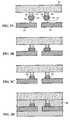
- FIG. 1shows a top view of a part of a leadframe
- FIG. 2shows a flowchart detailing a process for forming a FCOL semiconductor package with a semiconductor die and a leadframe
- FIGS. 3A-Dshows cross-sectional views of a part of the leadframe and the semiconductor die during the process in FIG. 1 .
- a predetermined amount of solderis deposited more uniformly on the free ends of copper posts extending from die pads of a semiconductor die.
- the solder depositsare coated with flux and the semiconductor die is then placed on a leadframe with the solder deposits abutting interconnect locations on inner lead portions of the leadframe.
- the solder depositsmelt and with the assistance of the flux forms solder interconnects between the free ends of the copper posts and the interconnect locations. Due to the predetermined amount of solder deposited on the free ends of the copper posts more uniformly, the molten solder tends not to flow away from the interconnect locations.
- advantageouslyallowing a substantial portion of the solder to remain at the interconnect locations resulting in more uniform solder interconnects.
- the assembly of the semiconductor die and the leadframeis encapsulated in mold compound with outer lead portions exposed and/or extending from the FCOL semiconductor package.
- a non-leaded version of the resultant packageis often referred to as the quad non-lead package (QFN).
- FIG. 1shows a part of a leadframe 100 , which has inner lead portions 101 , outer lead portions 102 and dam bar portions 103 .
- the outline 104indicates the location for placing a flipped semiconductor die (not shown) on the leadframe 100 .
- the inner lead portions 101which are coupled to the semiconductor die, will be enclosed with the semiconductor die in the FCOL semiconductor package, and th e , outer lead portions 102 will extend from the package.
- the dam bar portions 103define an outline of the FCOL package, and provide a seal during the molding process that encapsulates the semiconductor die and the inner lead portions 102 in the FCOL package.
- the dam bar portions 103 and other excess portions of the lead frame 100are removed during a subsequent trim and form operation after encapsulation or when the FCOL semiconductor package is singulated from the leadframe 100 .
- the leadframe 100is supplied by a vendor in a strip on which several FCOL semiconductor packages can be formed, as is known in the art. More commonly, the leadframe comprises copper and is plated with silver, nickel or palladium, however, the present invention also extends to use with un-plated leadframes, such as bare copper leadframes.
- the leadframe 100is a patterned metal leadframe, which provides a patterned layer of metal conductors, and can comprise a stamping from a sheet of metal, such as copper. Alternatively, the leadframe 100 can be produced by etching a copper sheet. When the thickness of the metal is relatively small, the leadframe 100 can comprise flexible circuits, also known as flex circuits, which includes a flexible substrate. In addition, the leadframe 100 , as referred to herein, extends to substrates including ceramic, laminate, polyimide substrate, and tape.
- a process 200 for forming a FCOL semiconductor packagestarts 205 with providing 210 the copper leadframe 100 .
- the process 200 as describedapplies to all copper posts 310 on the semiconductor die 305 and all the inner lead portions 101 of the leadframe 100 that form the FCOL semiconductor package.
- the semiconductor die 305is provided 215 , where the semiconductor die 305 includes copper posts 310 extending from pads (not shown) on the semiconductor die 305 as shown in FIG. 3A.
- a process for forming the copper posts 310 on the semiconductor die 305 when the die is part of a semiconductor waferwas alluded to earlier.
- a variety of other wafer bumping techniquesmay be employed to form non-reflowable bumps on a wafer, and the constituent bumped semiconductor dies of such wafers can be used in accordance with the present invention to form FCOL semiconductor packages.
- non-reflowable bumpsinclude gold, indium, tin, lead-free tin bismuth, lead free tin-copper, lead free tin-silver, and the like.
- FIG. 3Ashows the inner lead portions 101 of two adjacent leads of the leadframe 100 where each of the inner lead portions 101 has an interconnect location 335 thereon.
- An interconnect location hereinis defined as the area on the inner lead portion 101 when the copper posts 310 are aligned with the inner lead portions 101 i.e. the area bounded by the circumference of the copper posts 310 when the copper posts are aligned with the inner lead portions 101 , where the circumference of the copper posts are projected onto the inner lead portions 101 .
- the broken lines in FIGS. 3A and 3Cdefine the interconnect locations 335 on the inner lead portions 101 .
- the pattern of interconnect locations 335 on the inner lead portions 101corresponds to the pattern of copper posts 310 that extend from the semiconductor die 305 when the semiconductor die 315 is aligned with the inner lead portions 101 .
- solder deposits 315such as solder
- solder deposits 315are disposed 220 on the free ends of the copper posts 310 .
- the solder deposits 315can be disposed by a variety of techniques, as will be known to one skilled in the art. A reference cited earlier describes a process that disposes solder on the copper posts when the copper bumps are formed by electroplating.
- the amount of solder disposed on the end of each of the copper posts 310 of the semiconductor die 305is predetermined, and whatever process that is employed to dispose the solder, that process must ensure that the predetermined amount of solder is disposed on each of the copper post 310 .
- a plating processis used as the plating process has a lower process variation then that of the solder printing process. This allows the amount of solder disposed on the free ends of the copper posts to be better controlled and more uniform on a semiconductor die.
- the amount of solder disposedis dependent on a variety of factors which can include: type of solder, dimensions of the copper post, material at the interconnect location, mass of the semiconductor die, number of copper posts, reflow profile when reflowing the solder deposits 315 , the expected final dimensions of the reflowed solder and copper post, and the type of flux.
- This measured amount of the solderadvantageously allows a substantial portion of the disposed solder deposits 315 to remain at the interconnect locations 335 during reflow when the solder deposits 315 are in molten state.
- Flux 320is then applied or coated 225 on the solder deposits 315 . This is often achieved by briefly positioning the semiconductor die 305 with the solder deposits 315 immersed in a reservoir of the flux 320 . At elevated temperatures, the flux 320 cleans a surface to which it is applied to enhance the adhesion of the solder deposits 315 . The cleaned surfaces include the surface of the solder deposit 315 and the interconnect locations 335 .
- the semiconductor die 305is ready to be mounted on the leadframe 100 .
- the flux 320can be printed or disposed on the interconnect locations 335 , although this would require additional equipment relative to a single handler picking up the semiconductor die 305 with the solder, dipping the solder deposits 315 on the copper posts 310 in flux 320 and then placing the semiconductor die 305 on the leadframe 100 .
- the semiconductor die 305is positioned above the leadframe 100 with the solder deposits 315 aligned with the interconnect locations 335 on the leadframe 100 .
- the semiconductor die 305is then placed 230 on the leadframe 100 .
- the step of placinghere can include exerting and maintaining a predetermined force on the semiconductor die 305 against the leadframe 100 .
- the lower surface of the solder deposits 315abut the interconnect locations 335 , and the flux 320 on the solder deposits 315 flows around the solder deposits 315 and on the interconnect locations 335 .
- the flux 320 on the solder deposits 315wets or adheres to the interconnect locations 335 as shown in FIG. 3B, in preparation for the next step.
- the assembly of the semiconductor die 305 , the leadframe 100 , and the flux 320 ,is then reflowed 235 .
- Reflowing processeswill be known to one skilled in the art in relation to flip chip semiconductor packages, and no further detail is provided herein, except to the extent where such detail enhances the understanding of the present invention.
- the flux 320cleans the interconnect locations 335 on the leadframe 100 , and the solder deposits 315 change to a molten state.
- the molten solderflows onto the cleaned interconnect locations 335 , and adheres thereto forming a solder interconnect 340 between each of the copper posts 310 and the corresponding interconnect locations 335 , as shown in FIG. 3 C.
- the solder interconnect 340is sometimes called a fillet.
- the predetermined amount of solder 315 depositeddetermines the formation of the solder interconnect 340 , thus ensuring a substantial portion of the solder 315 deposited remains at the interconnect location 335 .
- the present inventionadvantageously, reduces the flow of solder away from the interconnect locations, thus, improving the coupling between the copper posts and the leadframe formed by the resultant solder interconnects.
- the assemblyAfter reflowing 235 , when normal flux is used, the assembly is cleaned to remove any access flux 320 , and the assembly is encapsulated 245 in mold compound 345 as shown in FIG. 3D, to produce a flip chip semiconductor package (not shown) on the leadframe 100 . Alternatively, when no-clean flux is employed, cleaning is not necessarily required. Subsequently, after a final step of singulating the FCOLF semiconductor package from the leadframe 100 , during which the dam bar portions 103 are severed, the process 200 ends 245 . As will be known to one skilled in the art, there may be the additional steps of forming the external lead portions 102 , and testing the functionality of the semiconductor die 320 , prior to singulation.
- An example of a semiconductor package formed in accordance with the present inventioncomprises a semiconductor die with copper post having a pitch of 250 microns, where the copper post has a length of 70 microns and a diameter of 100 microns.
- the solder plated on the free ends of the copper postshas a thickness of 30 microns, and the semiconductor die was mounted on a bare copper leadframe.
- the present inventionprovides a method of forming a flip chip semiconductor package on a leadframe where a predetermined amount of solder disposed on the copper posts on a semiconductor die tends to remain at interconnect locations on the leadframe.
- the present inventionprovides a method for forming a flip chip on leadframe semiconductor package, which overcomes or at least reduces the abovementioned problems of the prior art.
Landscapes
- Engineering & Computer Science (AREA)
- Computer Hardware Design (AREA)
- Microelectronics & Electronic Packaging (AREA)
- Power Engineering (AREA)
- Physics & Mathematics (AREA)
- Condensed Matter Physics & Semiconductors (AREA)
- General Physics & Mathematics (AREA)
- Lead Frames For Integrated Circuits (AREA)
- Wire Bonding (AREA)
Abstract
Description
The present invention relates to forming a flip chip semiconductor package on a leadframe, and more particularly to forming a flip chip semiconductor package with a bumped semiconductor die on a leadframe.
In semiconductor packaging, a relatively sensitive and difficult to handle semiconductor die is encapsulated in a package with external connections. Packaging allows the semiconductor die to be more conveniently handled, and it also allows external circuitry to be easily coupled thereto.
A known method of forming a flip chip on leadframe (FCOL) semiconductor package employs a plated leadframe. A leadframe is a patterned sheet of metal, typically copper, that has been plated, usually with silver, nickel or palladium. Conventionally, a leadframe is plated to prevent the copper from oxidizing, and to provide a surface to which solder will adhere. The pattern of the sheet of metal provides a leadframe for forming a semiconductor package.
Currently, leadframes for forming FCOL semiconductor packages have leads with inner lead portions and outer lead portions. The inner lead portions are arranged in a pattern with interconnect locations on the inner lead portions matching the pattern of pads on a semiconductor die. During the packaging process, typically eutectic solder is deposited on the interconnect locations. In addition, the pads on the semiconductor die are bumped. Bumping can comprise metal posts extending from the pads of the semiconductor die with solder balls on free ends of the metal posts. Typically, the solder balls are made of high lead solder.
U.S. patent application Ser. No. 09/564,382 by Francisca Tung, filed on Apr. 27, 2000, titled “Improved Pillar Connections For Semiconductor Chip”, and Continuation-In-Part U.S. patent application Ser. No. 09/843,248 by Francisca Tung, filed on Apr. 27, 2001 titled “Pillar Connections For Semiconductor Chips and Method Of Manufacture”, and assigned to a common assignee as this patent application, teaches forming pillar bump structures as described herein. These patent applications are incorporated herein by reference thereto.
Subsequently, the solder balls on the die, and the semiconductor die is flipped over, and placed on the leadframe, with the solder balls abutting the solder paste deposits on the interconnect locations. The assembly is then reflowed using an appropriate reflow profile.
Under the elevated reflow temperatures, the solder paste deposits melt, and with the assistance of the flux, the eutectic solder adheres to the interconnect locations on the leadframe and the high lead solder balls on the copper posts, thus forming solder interconnects between the high lead solder balls on the free ends of the metal posts and the interconnect locations on the leadframe. After reflow, when normal flux is used the assembly is cleaned to remove residual flux and encapsulated in mold compound. However, when no-clean flux is employed, the cleaning step is not necessarily required. The resultant package is known as a FCOL semiconductor package.
A disadvantage of this process is, when the solder paste melts, the molten solder tends to flows across the surface of the lead portions. This flow of solder is often referred to as overrun, and results in a variety of adverse effects in FCOL semiconductor packages.
A first concern is, when the solder flows away from an interconnect location, the respective solder interconnect constitutes less solder than required to provide a reliable electrical connection between the solder balls and the interconnect locations. A second concern is, solder interconnects formed with the reduced amount of solder do not support the semiconductor die evenly on the leadframe. Consequently, the planarity of the semiconductor die on the leadframe is adversely affected, and a non-planar die can give rise to shorting between the metal posts on the die. This condition is sometimes referred to as a collapsed die.
A third concern is the overrun results in solder flowing over the edges and onto the opposite surface of the lead portions. Later, during molding mold compound will not adhere well to the affected surfaces. A fourth concern is wicking, which occurs when a lead portion on a leadframe is shaped such that there is a small gap between the side of a downset die and the lead portion, and where there is an interconnect location close to the edge of the die. In this arrangement, the solder from the interconnect location can flow along the lead portion and, through capillary action, flow upwards through the small gap.
Further, eutectic solder paste is disposed on the interconnect locations using a printing process. This process of dispensing solder is known to suffer wide process variations. Consequently, the amount of solder paste dispensed on a leadframe can vary considerably. Such variations in the amount of solder paste dispensed for a particular semiconductor package leads to variations in the resultant solder joints, adversely affecting the reliability of the semiconductor package.
In an effort to reduce costs of producing FCOL semiconductor packages, un-plated or bare copper leadframes, simply referred to as copper leadframes, have been tried. However, to a large extent, the copper leadframes suffer the same disadvantages discussed hereinabove as the plated leadframe, and in some instances to a greater degree.
The present invention seeks to provide a method for forming a flip chip on leadframe semiconductor package, which overcomes or at least reduces the abovementioned problems of the prior art.
Accordingly, in one aspect, the present invention provides a method for forming a flip chip semiconductor package, the method comprising the steps of:
a) providing a patterned layer of metal conductors having a first surface for providing a pattern of interconnect locations thereon;
b) providing a semiconductor die having a first surface with a corresponding pattern of pads thereon, the pads having non-reflowable material thereon:
c) disposing a predetermined amount of reflowable conductive material on the non-reflowable material;
d) placing the semiconductor die on the patterned layer of metal conductors, wherein the reflowable conductive material abuts the interconnect locations; and
e) reflowing the reflowable conductive material, wherein a substantial portion of the reflowable conductive material remains substantially at the interconnect locations to form conductive interconnects between the non-reflowable material and the interconnect locations.
In another aspect the present invention provides a method for determining the amount of reflowable material to be disposed on non-reflowable bumps on a semiconductor die to mount the semiconductor die on a leadframe having interconnect locations thereon, the method comprising the steps of:
a) determining surface area of one of the non-reflowable bumps;
b) defining a corresponding interconnect location on the leadframe having substantially the same area as the surface area of the one of the non-reflowable bumps; and
c) selecting an amount of reflowable material such that a substantial portion of the selected amount of reflowable material remains at the interconnect location during reflow.
An embodiment of the present invention will now be more fully described, by way of example, with reference to the drawings of which:
FIG. 1 shows a top view of a part of a leadframe;
FIG. 2 shows a flowchart detailing a process for forming a FCOL semiconductor package with a semiconductor die and a leadframe; and
FIGS. 3A-D shows cross-sectional views of a part of the leadframe and the semiconductor die during the process in FIG.1.
A predetermined amount of solder is deposited more uniformly on the free ends of copper posts extending from die pads of a semiconductor die. The solder deposits are coated with flux and the semiconductor die is then placed on a leadframe with the solder deposits abutting interconnect locations on inner lead portions of the leadframe. When reflowed, the solder deposits melt and with the assistance of the flux forms solder interconnects between the free ends of the copper posts and the interconnect locations. Due to the predetermined amount of solder deposited on the free ends of the copper posts more uniformly, the molten solder tends not to flow away from the interconnect locations. Thus, advantageously allowing a substantial portion of the solder to remain at the interconnect locations resulting in more uniform solder interconnects. After forming the solder interconnects, the assembly of the semiconductor die and the leadframe is encapsulated in mold compound with outer lead portions exposed and/or extending from the FCOL semiconductor package. A non-leaded version of the resultant package is often referred to as the quad non-lead package (QFN).
FIG. 1 shows a part of aleadframe 100, which hasinner lead portions 101,outer lead portions 102 anddam bar portions 103. Theoutline 104 indicates the location for placing a flipped semiconductor die (not shown) on theleadframe 100. After a FCOL semiconductor package (not shown) is formed on theleadframe 100, theinner lead portions 101, which are coupled to the semiconductor die, will be enclosed with the semiconductor die in the FCOL semiconductor package, and th e ,outer lead portions 102 will extend from the package. Thedam bar portions 103 define an outline of the FCOL package, and provide a seal during the molding process that encapsulates the semiconductor die and theinner lead portions 102 in the FCOL package. Thedam bar portions 103 and other excess portions of thelead frame 100 are removed during a subsequent trim and form operation after encapsulation or when the FCOL semiconductor package is singulated from theleadframe 100. lypically, theleadframe 100 is supplied by a vendor in a strip on which several FCOL semiconductor packages can be formed, as is known in the art. More commonly, the leadframe comprises copper and is plated with silver, nickel or palladium, however, the present invention also extends to use with un-plated leadframes, such as bare copper leadframes.
Theleadframe 100 is a patterned metal leadframe, which provides a patterned layer of metal conductors, and can comprise a stamping from a sheet of metal, such as copper. Alternatively, theleadframe 100 can be produced by etching a copper sheet. When the thickness of the metal is relatively small, theleadframe 100 can comprise flexible circuits, also known as flex circuits, which includes a flexible substrate. In addition, theleadframe 100, as referred to herein, extends to substrates including ceramic, laminate, polyimide substrate, and tape.
With reference to FIG.2 and FIGS. 3A-D aprocess 200 for forming a FCOL semiconductor package, in accordance with the present invention, starts205 with providing210 thecopper leadframe 100. To facilitate description, only a portion of thelead frame 100 and a portion of asemiconductor die 305 are shown in FIGS. 3A-D. However, it will be appreciated by one skilled in the art, that theprocess 200 as described applies to allcopper posts 310 on the semiconductor die305 and all theinner lead portions 101 of theleadframe 100 that form the FCOL semiconductor package.
Next the semiconductor die305 is provided215, where the semiconductor die305 includescopper posts 310 extending from pads (not shown) on the semiconductor die305 as shown in FIG. 3A. A process for forming the copper posts310 on the semiconductor die305 when the die is part of a semiconductor wafer was alluded to earlier. A variety of other wafer bumping techniques may be employed to form non-reflowable bumps on a wafer, and the constituent bumped semiconductor dies of such wafers can be used in accordance with the present invention to form FCOL semiconductor packages. Examples of such non-reflowable bumps include gold, indium, tin, lead-free tin bismuth, lead free tin-copper, lead free tin-silver, and the like.
In addition, FIG. 3A shows theinner lead portions 101 of two adjacent leads of theleadframe 100 where each of theinner lead portions 101 has aninterconnect location 335 thereon. An interconnect location herein is defined as the area on theinner lead portion 101 when the copper posts310 are aligned with theinner lead portions 101 i.e. the area bounded by the circumference of the copper posts310 when the copper posts are aligned with theinner lead portions 101, where the circumference of the copper posts are projected onto theinner lead portions 101. The broken lines in FIGS. 3A and 3C define theinterconnect locations 335 on theinner lead portions 101. The pattern ofinterconnect locations 335 on theinner lead portions 101 corresponds to the pattern ofcopper posts 310 that extend from the semiconductor die305 when the semiconductor die315 is aligned with theinner lead portions 101.
Subsequently, reflowableconductive deposits 315, such as solder, is plated on or attached in the form of solder balls, on the free ends of the copper posts310. In this way thesolder deposits 315 are disposed220 on the free ends of the copper posts310. Thesolder deposits 315 can be disposed by a variety of techniques, as will be known to one skilled in the art. A reference cited earlier describes a process that disposes solder on the copper posts when the copper bumps are formed by electroplating.
The amount of solder disposed on the end of each of the copper posts310 of the semiconductor die305 is predetermined, and whatever process that is employed to dispose the solder, that process must ensure that the predetermined amount of solder is disposed on each of thecopper post 310. Here, a plating process is used as the plating process has a lower process variation then that of the solder printing process. This allows the amount of solder disposed on the free ends of the copper posts to be better controlled and more uniform on a semiconductor die. The amount of solder disposed is dependent on a variety of factors which can include: type of solder, dimensions of the copper post, material at the interconnect location, mass of the semiconductor die, number of copper posts, reflow profile when reflowing thesolder deposits 315, the expected final dimensions of the reflowed solder and copper post, and the type of flux. This measured amount of the solder, advantageously allows a substantial portion of thedisposed solder deposits 315 to remain at theinterconnect locations 335 during reflow when thesolder deposits 315 are in molten state.
After theflux 320 is applied, the semiconductor die305 is ready to be mounted on theleadframe 100. Alternatively, theflux 320 can be printed or disposed on theinterconnect locations 335, although this would require additional equipment relative to a single handler picking up the semiconductor die305 with the solder, dipping thesolder deposits 315 on the copper posts310 influx 320 and then placing the semiconductor die305 on theleadframe 100.
After applying theflux 320, the semiconductor die305 is positioned above theleadframe 100 with thesolder deposits 315 aligned with theinterconnect locations 335 on theleadframe 100. The semiconductor die305 is then placed230 on theleadframe 100. The step of placing here can include exerting and maintaining a predetermined force on the semiconductor die305 against theleadframe 100.
When the semiconductor die305 is placed on theleadframe 100, the lower surface of thesolder deposits 315 abut theinterconnect locations 335, and theflux 320 on thesolder deposits 315 flows around thesolder deposits 315 and on theinterconnect locations 335. Theflux 320 on thesolder deposits 315 wets or adheres to theinterconnect locations 335 as shown in FIG. 3B, in preparation for the next step.
The assembly of the semiconductor die305, theleadframe 100, and theflux 320, is then reflowed235. Reflowing processes will be known to one skilled in the art in relation to flip chip semiconductor packages, and no further detail is provided herein, except to the extent where such detail enhances the understanding of the present invention. Duringreflow 235, theflux 320 cleans theinterconnect locations 335 on theleadframe 100, and thesolder deposits 315 change to a molten state. The molten solder flows onto the cleanedinterconnect locations 335, and adheres thereto forming asolder interconnect 340 between each of the copper posts310 and the correspondinginterconnect locations 335, as shown in FIG.3C.
Thesolder interconnect 340 is sometimes called a fillet. The predetermined amount ofsolder 315 deposited determines the formation of thesolder interconnect 340, thus ensuring a substantial portion of thesolder 315 deposited remains at theinterconnect location 335.
Consequently, there is more solder at theinterconnect locations 335, which increases the mechanical strength of the coupling between the copper posts310 and theleadframe 100, thus producing more reliable electrical coupling.
Hence, the present invention, as described, advantageously, reduces the flow of solder away from the interconnect locations, thus, improving the coupling between the copper posts and the leadframe formed by the resultant solder interconnects.
After reflowing235, when normal flux is used, the assembly is cleaned to remove anyaccess flux 320, and the assembly is encapsulated245 inmold compound 345 as shown in FIG. 3D, to produce a flip chip semiconductor package (not shown) on theleadframe 100. Alternatively, when no-clean flux is employed, cleaning is not necessarily required. Subsequently, after a final step of singulating the FCOLF semiconductor package from theleadframe 100, during which thedam bar portions 103 are severed, theprocess 200 ends245. As will be known to one skilled in the art, there may be the additional steps of forming theexternal lead portions 102, and testing the functionality of the semiconductor die320, prior to singulation.
An example of a semiconductor package formed in accordance with the present invention comprises a semiconductor die with copper post having a pitch of 250 microns, where the copper post has a length of 70 microns and a diameter of 100 microns. The solder plated on the free ends of the copper posts has a thickness of 30 microns, and the semiconductor die was mounted on a bare copper leadframe.
The present invention, as described, provides a method of forming a flip chip semiconductor package on a leadframe where a predetermined amount of solder disposed on the copper posts on a semiconductor die tends to remain at interconnect locations on the leadframe.
This is accomplished by determining the amount of solder to be disposed taking into account a variety of factors including type of solder, the dimensions of the metal post, the material at the interconnect location, the mass of the die, the number of metal posts, the reflow profile, the expected final dimensions of the reflowed solder and copper post and the type of flux.
Thus, the present invention, as described provides a method for forming a flip chip on leadframe semiconductor package, which overcomes or at least reduces the abovementioned problems of the prior art.
It will be appreciated that although only one particular embodiment of the invention has been described in detail, various modifications and improvements can be made by a person skilled in the art without departing from the scope of the present invention.
Claims (23)
1. A method for forming a flip chip semiconductor package, the method comprising the steps of:
a) providing a patterned layer of metal conductors having a first surface;
b) providing a semiconductor die having a first surface with a pattern of pads thereon, the pads having non-reflowable material thereon, wherein the pattern of pads is different from the patterned layer of metal conductors, and wherein the non-reflowable material melts at a temperature that is higher than a predetermined reflow temperature;
c) disposing a predetermined amount of reflowable conductive material on free-ends of the non-reflowable material on each of the pads, wherein the reflowable conductive material melts at the predetermined reflow temperature;
d) placing the semiconductor die on the first surface of the patterned layer of metal conductors, wherein the reflowable conductive material on the non-reflowable material on each of the pads abut the patterned layer of metal conductors to form a pattern of interconnect locations on the patterned layer of metal conductors, and wherein the pattern of interconnect locations correspond with the pattern of pads; and
e) reflowing the reflowable conductive material at the predetermined reflow temperature, wherein a substantial portion of the reflowable conductive material on the non-reflowable material on the each of the pads remains substantially at the respective interconnect locations to form conductive interconnects between the non-reflowable material and the interconnect locations.
2. A method in accordance withclaim 1 wherein step (c) comprises the step of determining the predetermined amount of reflowable conductive material based on material composition of the reflowable conductive material.
3. A method in accordance withclaim 1 wherein step (c) comprises the step of determining the predetermined amount of reflowable conductive material based on material composition of the interconnect locations.
4. A method in accordance withclaim 1 wherein step (c) comprises the step of determining the predetermined amount of reflowable conductive material based on material composition of the non-reflowable material.
5. A method in accordance withclaim 1 wherein step (c) comprises the step of determining the predetermined amount of reflowable conductive material based on dimensions of the non-reflowable material.
6. A method in accordance withclaim 1 wherein step (c) comprises the step of determining the predetermined amount of reflowable conductive material based on mass of the semiconductor die.
7. A method in accordance withclaim 1 wherein step (c) comprises the step of determining the predetermined amount of reflowable conductive material based on number of pads having non-reflowable material thereon.
8. A method in accordance withclaim 1 wherein step (c) comprises the step of determining the predetermined amount of reflowable conductive material based on expected final dimensions of reflowed reflowable material.
9. A method in accordance withclaim 1 wherein step (c) comprises the step of plating the predetermined amount of reflowable conductive material on the non-reflowable material.
10. A method in accordance withclaim 1 further comprising after step (c) and before step (d), the step of applying a cleaning agent.
11. A method in accordance withclaim 10 comprising the step of applying a cleaning agent to the reflowable conductive material.
12. A method in accordance withclaim 10 wherein step (c) comprises the step of determining the predetermined amount of reflowable conductive material based on material composition of the cleaning agent.
13. A method in accordance withclaim 1 wherein step (a) comprises the step of providing the patterned layer of metal conductors having a first surface with a layer of plating thereon.
14. A method in accordance withclaim 13 wherein step (c) comprises the step of determining the predetermined amount of reflowable conductive material based on material composition of the layer of plating.
15. A method in accordance withclaim 1 wherein step (a) comprises the step of providing the patterned layer of copper conductors.
16. A method in accordance withclaim 15 wherein step (a) further comprises the step of providing a layer of plating on the first surface of the patterned layer of copper conductors.
17. A method in accordance withclaim 15 wherein step (b) comprises the step of providing a semiconductor die having the first surface with the corresponding pattern of pads thereon, the pads having copper posts thereon and extending therefrom.
18. A method in accordance withclaim 17 wherein step (c) comprises the step of disposing a predetermined amount of solder on free ends of the copper posts.
19. A method in accordance withclaim 18 after step (c) and before step (d) comprising the step of applying flux to the solder.
20. A method in accordance withclaim 19 after the step of applying flux to the solder, the step of cleaning the semiconductor die and the patterned layer of copper conductors.
21. A method in accordance withclaim 20 further comprising after the step of cleaning, the step of encapsulating at least a part of the semiconductor die and at least a part of the patterned layer of copper conductors to form a semiconductor package.
22. A method in accordance withclaim 21 , wherein the patterned layer of copper conductors comprises a portion of a leadframe, wherein the step of encapsulating at least a part of the semiconductor die and at least a part of the patterned layer of copper conductors to form a semiconductor package comprises the step of encapsulating at least the part of the semiconductor die and at least a part of the portion of the leadframe to form the semiconductor package, and further comprises after the step of encapsulating, the step of singulating the semiconductor package from the leadframe.
23. A method in accordance withclaim 21 wherein the step of encapsulating comprises the step of molding.
Priority Applications (3)
| Application Number | Priority Date | Filing Date | Title |
|---|---|---|---|
| US09/934,019US6550666B2 (en) | 2001-08-21 | 2001-08-21 | Method for forming a flip chip on leadframe semiconductor package |
| CNB028038002ACN100521130C (en) | 2001-08-21 | 2002-08-20 | Method for forming a flip chip on leadframe semiconductor package |
| PCT/SG2002/000189WO2003017366A1 (en) | 2001-08-21 | 2002-08-20 | Method for forming a flip chip on leadframe semiconductor package |
Applications Claiming Priority (1)
| Application Number | Priority Date | Filing Date | Title |
|---|---|---|---|
| US09/934,019US6550666B2 (en) | 2001-08-21 | 2001-08-21 | Method for forming a flip chip on leadframe semiconductor package |
Publications (2)
| Publication Number | Publication Date |
|---|---|
| US20030038162A1 US20030038162A1 (en) | 2003-02-27 |
| US6550666B2true US6550666B2 (en) | 2003-04-22 |
Family
ID=25464823
Family Applications (1)
| Application Number | Title | Priority Date | Filing Date |
|---|---|---|---|
| US09/934,019Expired - LifetimeUS6550666B2 (en) | 2001-08-21 | 2001-08-21 | Method for forming a flip chip on leadframe semiconductor package |
Country Status (3)
| Country | Link |
|---|---|
| US (1) | US6550666B2 (en) |
| CN (1) | CN100521130C (en) |
| WO (1) | WO2003017366A1 (en) |
Cited By (112)
| Publication number | Priority date | Publication date | Assignee | Title |
|---|---|---|---|---|
| US20040222518A1 (en)* | 2003-02-25 | 2004-11-11 | Tessera, Inc. | Ball grid array with bumps |
| US20050077624A1 (en)* | 2003-10-09 | 2005-04-14 | Advanpack Solutions Pte. Ltd. | Pillar structures |
| US20050116326A1 (en)* | 2003-10-06 | 2005-06-02 | Tessera, Inc. | Formation of circuitry with modification of feature height |
| US20050168231A1 (en)* | 2003-12-24 | 2005-08-04 | Young-Gon Kim | Methods and structures for electronic probing arrays |
| US20050173805A1 (en)* | 2003-12-30 | 2005-08-11 | Tessera, Inc. | Micro pin grid array with pin motion isolation |
| US20050181544A1 (en)* | 2003-12-30 | 2005-08-18 | Tessera, Inc. | Microelectronic packages and methods therefor |
| US20050181655A1 (en)* | 2003-12-30 | 2005-08-18 | Tessera, Inc. | Micro pin grid array with wiping action |
| US20050284658A1 (en)* | 2003-10-06 | 2005-12-29 | Tessera, Inc. | Components with posts and pads |
| US20060040488A1 (en)* | 1994-12-29 | 2006-02-23 | Tessera, Inc. | Method of electrically connecting a microelectronic component |
| US20070040237A1 (en)* | 2005-08-22 | 2007-02-22 | Coyle Anthony L | High current semiconductor device system having low resistance and inductance |
| US20070148822A1 (en)* | 2005-12-23 | 2007-06-28 | Tessera, Inc. | Microelectronic packages and methods therefor |
| US20070148819A1 (en)* | 2005-12-23 | 2007-06-28 | Tessera, Inc. | Microelectronic assemblies having very fine pitch stacking |
| US20070205496A1 (en)* | 2004-06-25 | 2007-09-06 | Tessera, Inc. | Microelectronic packages and methods therefor |
| US20070284420A1 (en)* | 2006-06-13 | 2007-12-13 | Advanpack Solutions Pte Ltd | Integrated circuit chip formed on substrate |
| US20080003402A1 (en)* | 2003-10-06 | 2008-01-03 | Tessera, Inc. | Fine pitch microcontacts and method for forming thereof |
| US20080042250A1 (en)* | 2006-08-18 | 2008-02-21 | Tessera, Inc. | Stacked microelectronic assemblies and methods therefor |
| US20080078813A1 (en)* | 2006-09-29 | 2008-04-03 | Chi-Won Hwang | Carbon nanotube-reinforced solder caps, methods of assembling same, and chip packages and systems containing same |
| US20080090427A1 (en)* | 2006-10-12 | 2008-04-17 | Tessera, Inc. | Microelectronic component with foam-metal posts |
| US20080088033A1 (en)* | 2006-10-17 | 2008-04-17 | Tessera, Inc. | Microelectronic packages and methods therefor |
| US20080150101A1 (en)* | 2006-12-20 | 2008-06-26 | Tessera, Inc. | Microelectronic packages having improved input/output connections and methods therefor |
| US20090085203A1 (en)* | 2006-02-13 | 2009-04-02 | Htc Beteiligungs Gmbh | Method for Exchanging Semiconductor Chip of Flip-Chip Module and Flip-Chip Module Suitable Therefor |
| US20090108443A1 (en)* | 2007-10-30 | 2009-04-30 | Monolithic Power Systems, Inc. | Flip-Chip Interconnect Structure |
| US20100044860A1 (en)* | 2008-08-21 | 2010-02-25 | Tessera Interconnect Materials, Inc. | Microelectronic substrate or element having conductive pads and metal posts joined thereto using bond layer |
| US20110001232A1 (en)* | 2005-09-14 | 2011-01-06 | Htc Beteiligungs Gmbh | Flip-Chip Module and Method for the Production Thereof |
| US20110084386A1 (en)* | 2003-11-10 | 2011-04-14 | Stats Chippac, Ltd. | Semiconductor Device and Method of Self-Confinement of Conductive Bump Material During Reflow Without Solder Mask |
| US20110084389A1 (en)* | 2009-10-14 | 2011-04-14 | Jian-Wen Lo | Semiconductor Device |
| US20110084381A1 (en)* | 2009-10-14 | 2011-04-14 | Jian-Wen Lo | Chip Having A Metal Pillar Structure |
| US7939934B2 (en) | 2005-03-16 | 2011-05-10 | Tessera, Inc. | Microelectronic packages and methods therefor |
| US20110121464A1 (en)* | 2009-11-24 | 2011-05-26 | Stats Chippac, Ltd. | Semiconductor Device and Method of Forming Electrical Interconnect with Stress Relief Void |
| US8183129B2 (en) | 2005-09-07 | 2012-05-22 | Infineon Technologies Ag | Alignment marks for polarized light lithography and method for use thereof |
| US8330272B2 (en) | 2010-07-08 | 2012-12-11 | Tessera, Inc. | Microelectronic packages with dual or multiple-etched flip-chip connectors |
| US8404520B1 (en) | 2011-10-17 | 2013-03-26 | Invensas Corporation | Package-on-package assembly with wire bond vias |
| US8482111B2 (en) | 2010-07-19 | 2013-07-09 | Tessera, Inc. | Stackable molded microelectronic packages |
| US8492893B1 (en) | 2011-03-16 | 2013-07-23 | Amkor Technology, Inc. | Semiconductor device capable of preventing dielectric layer from cracking |
| US8525314B2 (en) | 2004-11-03 | 2013-09-03 | Tessera, Inc. | Stacked packaging improvements |
| US8536458B1 (en) | 2009-03-30 | 2013-09-17 | Amkor Technology, Inc. | Fine pitch copper pillar package and method |
| US8569885B2 (en) | 2010-10-29 | 2013-10-29 | Advanced Semiconductor Engineering, Inc. | Stacked semiconductor packages and related methods |
| US8580607B2 (en) | 2010-07-27 | 2013-11-12 | Tessera, Inc. | Microelectronic packages with nanoparticle joining |
| US8623706B2 (en) | 2010-11-15 | 2014-01-07 | Tessera, Inc. | Microelectronic package with terminals on dielectric mass |
| US8686568B2 (en) | 2012-09-27 | 2014-04-01 | Advanced Semiconductor Engineering, Inc. | Semiconductor package substrates having layered circuit segments, and related methods |
| US8698307B2 (en) | 2010-09-27 | 2014-04-15 | Advanced Semiconductor Engineering, Inc. | Semiconductor package with integrated metal pillars and manufacturing methods thereof |
| US8716790B2 (en) | 2004-01-29 | 2014-05-06 | Enpirion, Inc. | Laterally diffused metal oxide semiconductor device and method of forming the same |
| EP2738807A2 (en) | 2012-11-30 | 2014-06-04 | Enpirion, Inc. | An apparatus including a semiconductor device coupled to a decoupling device |
| US8810029B2 (en) | 2003-11-10 | 2014-08-19 | Stats Chippac, Ltd. | Solder joint flip chip interconnection |
| US8835228B2 (en) | 2012-05-22 | 2014-09-16 | Invensas Corporation | Substrate-less stackable package with wire-bond interconnect |
| US8841779B2 (en) | 2005-03-25 | 2014-09-23 | Stats Chippac, Ltd. | Semiconductor device and method of forming high routing density BOL BONL and BONP interconnect sites on substrate |
| US8853558B2 (en) | 2010-12-10 | 2014-10-07 | Tessera, Inc. | Interconnect structure |
| US8872318B2 (en) | 2011-08-24 | 2014-10-28 | Tessera, Inc. | Through interposer wire bond using low CTE interposer with coarse slot apertures |
| US8878353B2 (en) | 2012-12-20 | 2014-11-04 | Invensas Corporation | Structure for microelectronic packaging with bond elements to encapsulation surface |
| US8884448B2 (en) | 2007-09-28 | 2014-11-11 | Tessera, Inc. | Flip chip interconnection with double post |
| US8884443B2 (en) | 2012-07-05 | 2014-11-11 | Advanced Semiconductor Engineering, Inc. | Substrate for semiconductor package and process for manufacturing |
| US8883563B1 (en) | 2013-07-15 | 2014-11-11 | Invensas Corporation | Fabrication of microelectronic assemblies having stack terminals coupled by connectors extending through encapsulation |
| US8975738B2 (en) | 2012-11-12 | 2015-03-10 | Invensas Corporation | Structure for microelectronic packaging with terminals on dielectric mass |
| US8987815B2 (en) | 2004-01-29 | 2015-03-24 | Enpirion, Inc. | Integrated circuit with a laterally diffused metal oxide semiconductor device and method of forming the same |
| US9023691B2 (en) | 2013-07-15 | 2015-05-05 | Invensas Corporation | Microelectronic assemblies with stack terminals coupled by connectors extending through encapsulation |
| US9034696B2 (en) | 2013-07-15 | 2015-05-19 | Invensas Corporation | Microelectronic assemblies having reinforcing collars on connectors extending through encapsulation |
| US9064858B2 (en) | 2003-11-10 | 2015-06-23 | Stats Chippac, Ltd. | Semiconductor device and method of forming bump-on-lead interconnection |
| US9082753B2 (en) | 2013-11-12 | 2015-07-14 | Invensas Corporation | Severing bond wire by kinking and twisting |
| US9087815B2 (en) | 2013-11-12 | 2015-07-21 | Invensas Corporation | Off substrate kinking of bond wire |
| US9093435B2 (en) | 2011-05-03 | 2015-07-28 | Tessera, Inc. | Package-on-package assembly with wire bonds to encapsulation surface |
| US9137903B2 (en) | 2010-12-21 | 2015-09-15 | Tessera, Inc. | Semiconductor chip assembly and method for making same |
| US9159708B2 (en) | 2010-07-19 | 2015-10-13 | Tessera, Inc. | Stackable molded microelectronic packages with area array unit connectors |
| US9159665B2 (en) | 2005-03-25 | 2015-10-13 | Stats Chippac, Ltd. | Flip chip interconnection having narrow interconnection sites on the substrate |
| US9177899B2 (en) | 2012-07-31 | 2015-11-03 | Mediatek Inc. | Semiconductor package and method for fabricating base for semiconductor package |
| US9214454B2 (en) | 2014-03-31 | 2015-12-15 | Invensas Corporation | Batch process fabrication of package-on-package microelectronic assemblies |
| US9219045B2 (en) | 2003-11-10 | 2015-12-22 | Stats Chippac, Ltd. | Semiconductor device and method of self-confinement of conductive bump material during reflow without solder mask |
| US9224717B2 (en) | 2011-05-03 | 2015-12-29 | Tessera, Inc. | Package-on-package assembly with wire bonds to encapsulation surface |
| US9324681B2 (en) | 2010-12-13 | 2016-04-26 | Tessera, Inc. | Pin attachment |
| US9349706B2 (en) | 2012-02-24 | 2016-05-24 | Invensas Corporation | Method for package-on-package assembly with wire bonds to encapsulation surface |
| US9391008B2 (en) | 2012-07-31 | 2016-07-12 | Invensas Corporation | Reconstituted wafer-level package DRAM |
| US9412714B2 (en) | 2014-05-30 | 2016-08-09 | Invensas Corporation | Wire bond support structure and microelectronic package including wire bonds therefrom |
| US9502390B2 (en) | 2012-08-03 | 2016-11-22 | Invensas Corporation | BVA interposer |
| US9536938B1 (en) | 2013-11-27 | 2017-01-03 | Altera Corporation | Semiconductor device including a resistor metallic layer and method of forming the same |
| US9583411B2 (en) | 2014-01-17 | 2017-02-28 | Invensas Corporation | Fine pitch BVA using reconstituted wafer with area array accessible for testing |
| US9601454B2 (en) | 2013-02-01 | 2017-03-21 | Invensas Corporation | Method of forming a component having wire bonds and a stiffening layer |
| US9633971B2 (en) | 2015-07-10 | 2017-04-25 | Invensas Corporation | Structures and methods for low temperature bonding using nanoparticles |
| US9646917B2 (en) | 2014-05-29 | 2017-05-09 | Invensas Corporation | Low CTE component with wire bond interconnects |
| US9659848B1 (en) | 2015-11-18 | 2017-05-23 | Invensas Corporation | Stiffened wires for offset BVA |
| US9673192B1 (en) | 2013-11-27 | 2017-06-06 | Altera Corporation | Semiconductor device including a resistor metallic layer and method of forming the same |
| US9685365B2 (en) | 2013-08-08 | 2017-06-20 | Invensas Corporation | Method of forming a wire bond having a free end |
| US9691679B2 (en) | 2012-02-24 | 2017-06-27 | Invensas Corporation | Method for package-on-package assembly with wire bonds to encapsulation surface |
| USRE46466E1 (en)* | 2005-09-01 | 2017-07-04 | Texas Instruments Incorporated | Method for fabricating low resistance, low inductance interconnections in high current semiconductor devices |
| US9728527B2 (en) | 2013-11-22 | 2017-08-08 | Invensas Corporation | Multiple bond via arrays of different wire heights on a same substrate |
| US9735084B2 (en) | 2014-12-11 | 2017-08-15 | Invensas Corporation | Bond via array for thermal conductivity |
| US9761554B2 (en) | 2015-05-07 | 2017-09-12 | Invensas Corporation | Ball bonding metal wire bond wires to metal pads |
| US9773685B2 (en) | 2003-11-10 | 2017-09-26 | STATS ChipPAC Pte. Ltd. | Solder joint flip chip interconnection having relief structure |
| US9793877B2 (en) | 2013-12-17 | 2017-10-17 | Avago Technologies General Ip (Singapore) Pte. Ltd. | Encapsulated bulk acoustic wave (BAW) resonator device |
| US9812402B2 (en) | 2015-10-12 | 2017-11-07 | Invensas Corporation | Wire bond wires for interference shielding |
| US9842745B2 (en) | 2012-02-17 | 2017-12-12 | Invensas Corporation | Heat spreading substrate with embedded interconnects |
| US9852969B2 (en) | 2013-11-22 | 2017-12-26 | Invensas Corporation | Die stacks with one or more bond via arrays of wire bond wires and with one or more arrays of bump interconnects |
| US9888579B2 (en)* | 2015-03-05 | 2018-02-06 | Invensas Corporation | Pressing of wire bond wire tips to provide bent-over tips |
| US9911718B2 (en) | 2015-11-17 | 2018-03-06 | Invensas Corporation | ‘RDL-First’ packaged microelectronic device for a package-on-package device |
| US9922915B2 (en) | 2003-11-10 | 2018-03-20 | STATS ChipPAC Pte. Ltd. | Bump-on-lead flip chip interconnection |
| US9935075B2 (en) | 2016-07-29 | 2018-04-03 | Invensas Corporation | Wire bonding method and apparatus for electromagnetic interference shielding |
| US9984992B2 (en) | 2015-12-30 | 2018-05-29 | Invensas Corporation | Embedded wire bond wires for vertical integration with separate surface mount and wire bond mounting surfaces |
| US10008469B2 (en) | 2015-04-30 | 2018-06-26 | Invensas Corporation | Wafer-level packaging using wire bond wires in place of a redistribution layer |
| US10008477B2 (en) | 2013-09-16 | 2018-06-26 | Invensas Corporation | Microelectronic element with bond elements to encapsulation surface |
| US10020739B2 (en) | 2014-03-27 | 2018-07-10 | Altera Corporation | Integrated current replicator and method of operating the same |
| US10026717B2 (en) | 2013-11-22 | 2018-07-17 | Invensas Corporation | Multiple bond via arrays of different wire heights on a same substrate |
| US10103627B2 (en) | 2015-02-26 | 2018-10-16 | Altera Corporation | Packaged integrated circuit including a switch-mode regulator and method of forming the same |
| US10181457B2 (en) | 2015-10-26 | 2019-01-15 | Invensas Corporation | Microelectronic package for wafer-level chip scale packaging with fan-out |
| US10299368B2 (en) | 2016-12-21 | 2019-05-21 | Invensas Corporation | Surface integrated waveguides and circuit structures therefor |
| US10332854B2 (en) | 2015-10-23 | 2019-06-25 | Invensas Corporation | Anchoring structure of fine pitch bva |
| US10381326B2 (en) | 2014-05-28 | 2019-08-13 | Invensas Corporation | Structure and method for integrated circuits packaging with increased density |
| USRE47600E1 (en) | 2003-11-10 | 2019-09-10 | STATS ChipPAC Pte. Ltd. | Semiconductor device and method of forming electrical interconnect with stress relief void |
| US10460958B2 (en) | 2013-08-07 | 2019-10-29 | Invensas Corporation | Method of manufacturing embedded packaging with preformed vias |
| US10490528B2 (en) | 2015-10-12 | 2019-11-26 | Invensas Corporation | Embedded wire bond wires |
| US10535626B2 (en) | 2015-07-10 | 2020-01-14 | Invensas Corporation | Structures and methods for low temperature bonding using nanoparticles |
| US10573615B2 (en) | 2012-07-31 | 2020-02-25 | Mediatek Inc. | Semiconductor package and method for fabricating base for semiconductor package |
| US10991669B2 (en) | 2012-07-31 | 2021-04-27 | Mediatek Inc. | Semiconductor package using flip-chip technology |
| US11973056B2 (en) | 2016-10-27 | 2024-04-30 | Adeia Semiconductor Technologies Llc | Methods for low temperature bonding using nanoparticles |
| US12211809B2 (en) | 2020-12-30 | 2025-01-28 | Adeia Semiconductor Bonding Technologies Inc. | Structure with conductive feature and method of forming same |
Families Citing this family (21)
| Publication number | Priority date | Publication date | Assignee | Title |
|---|---|---|---|---|
| DE10158770B4 (en)* | 2001-11-29 | 2006-08-03 | Infineon Technologies Ag | Lead frame and component with a lead frame |
| TW200423344A (en)* | 2002-12-31 | 2004-11-01 | Texas Instruments Inc | Composite metal column for mounting semiconductor device |
| US7550852B2 (en) | 2002-12-31 | 2009-06-23 | Texas Instruments Incorporated | Composite metal column for mounting semiconductor device |
| JP3994095B2 (en)* | 2004-06-23 | 2007-10-17 | ローム株式会社 | Surface mount electronic components |
| KR100755686B1 (en)* | 2005-01-04 | 2007-09-05 | 삼성전자주식회사 | Signal amplification device and method |
| US20060226199A1 (en)* | 2005-03-30 | 2006-10-12 | Visteon Global Technologies, Inc. | Selective soldering of flat flexible cable with lead-free solder to a substrate |
| US20090014852A1 (en)* | 2007-07-11 | 2009-01-15 | Hsin-Hui Lee | Flip-Chip Packaging with Stud Bumps |
| US7691670B2 (en) | 2008-05-01 | 2010-04-06 | Gem Services, Inc. | Interconnection of lead frame to die utilizing flip chip process |
| TWI502706B (en)* | 2009-10-29 | 2015-10-01 | Taiwan Semiconductor Mfg Co Ltd | Robust joint structure for flip-chip bonding |
| CN101807532B (en)* | 2010-03-30 | 2012-05-09 | 上海凯虹科技电子有限公司 | Flip-chip packaging method and packaging body of ultrathin chip |
| CN102049580B (en)* | 2010-09-26 | 2013-04-24 | 广州金升阳科技有限公司 | Welding method of lead frame |
| CN103752970B (en)* | 2013-12-24 | 2017-09-22 | 广州金升阳科技有限公司 | A kind of welding method of lead frame |
| US9642261B2 (en)* | 2014-01-24 | 2017-05-02 | Zhuhai Advanced Chip Carriers & Electronic Substrate Solutions Technologies Co. Ltd. | Composite electronic structure with partially exposed and protruding copper termination posts |
| CN104392941B (en)* | 2014-10-31 | 2017-11-03 | 通富微电子股份有限公司 | The method for forming flip chip semiconductor package |
| TWI556368B (en)* | 2015-01-16 | 2016-11-01 | 南茂科技股份有限公司 | Chip package structure and manufacturing method thereof |
| US10636758B2 (en)* | 2017-10-05 | 2020-04-28 | Texas Instruments Incorporated | Expanded head pillar for bump bonds |
| KR102817931B1 (en) | 2018-11-28 | 2025-06-09 | 오토스토어 테크놀로지 에이에스 | Storage containers for automatic storage and retrieval systems |
| DE102019115369A1 (en)* | 2019-06-06 | 2020-12-10 | Infineon Technologies Ag | METHOD OF MANUFACTURING A SEMICONDUCTOR FLIP CHIP PACKAGE |
| NO345453B1 (en) | 2019-06-28 | 2021-02-08 | Autostore Tech As | System and method for light communication in a storage system |
| US20220059439A1 (en)* | 2020-08-21 | 2022-02-24 | Texas Instruments Incorporated | Solder printing |
| NO20211250A1 (en) | 2021-10-18 | 2023-04-19 | Autostore Tech As | A service vehicle for an automated storage and retrieval system |
Citations (23)
| Publication number | Priority date | Publication date | Assignee | Title |
|---|---|---|---|---|
| US4914814A (en)* | 1989-05-04 | 1990-04-10 | International Business Machines Corporation | Process of fabricating a circuit package |
| US5634268A (en)* | 1995-06-07 | 1997-06-03 | International Business Machines Corporation | Method for making direct chip attach circuit card |
| US5640052A (en)* | 1993-03-10 | 1997-06-17 | Nec Corporation | Interconnection structure of electronic parts |
| US5723904A (en)* | 1993-03-10 | 1998-03-03 | Sumitomo Electric Industries, Ltd. | Packaged semiconductor device suitable to be mounted and connected to microstrip line structure board |
| US5747101A (en)* | 1994-02-02 | 1998-05-05 | International Business Machines Corporation | Direct chip attachment (DCA) with electrically conductive adhesives |
| US5796591A (en)* | 1995-06-07 | 1998-08-18 | International Business Machines Corporation | Direct chip attach circuit card |
| US5889326A (en)* | 1996-02-27 | 1999-03-30 | Nec Corporation | Structure for bonding semiconductor device to substrate |
| US6011313A (en)* | 1997-06-23 | 2000-01-04 | Ford Motor Company | Flip chip interconnections on electronic modules |
| US6024275A (en)* | 1997-06-18 | 2000-02-15 | National Semiconductor Corporation | Method of making flip chip and BGA interconnections |
| US6107180A (en)* | 1998-01-30 | 2000-08-22 | Motorola, Inc. | Method for forming interconnect bumps on a semiconductor die |
| US6114187A (en)* | 1997-01-11 | 2000-09-05 | Microfab Technologies, Inc. | Method for preparing a chip scale package and product produced by the method |
| US6165885A (en)* | 1995-08-02 | 2000-12-26 | International Business Machines Corporation | Method of making components with solder balls |
| US6177636B1 (en)* | 1994-12-29 | 2001-01-23 | Tessera, Inc. | Connection components with posts |
| US6196443B1 (en)* | 1997-07-22 | 2001-03-06 | International Business Machines Corporation | Pb-In-Sn tall C-4 for fatigue enhancement |
| EP1080889A2 (en)* | 1999-09-06 | 2001-03-07 | FUJI MACHINE Mfg. Co., Ltd. | Method and apparatus fpr controlling pressure applied to printing material |
| US6303872B1 (en)* | 1997-06-25 | 2001-10-16 | Visteon Global Tech. | Anti-tombstoning solder joints |
| US6337445B1 (en)* | 1998-03-16 | 2002-01-08 | Texas Instruments Incorporated | Composite connection structure and method of manufacturing |
| US6344234B1 (en)* | 1995-06-07 | 2002-02-05 | International Business Machines Corportion | Method for forming reflowed solder ball with low melting point metal cap |
| US6350668B1 (en)* | 1999-06-07 | 2002-02-26 | Kishore K. Chakravorty | Low cost chip size package and method of fabricating the same |
| US6363295B1 (en)* | 1997-06-06 | 2002-03-26 | Micron Technology, Inc. | Method for using data regarding manufacturing procedures integrated circuits (IC's) have undergone, such as repairs, to select procedures the IC's will undergo, such as additional repairs |
| US6372624B1 (en)* | 1997-08-04 | 2002-04-16 | Micron Technology, Inc. | Method for fabricating solder bumps by wave soldering |
| US6380555B1 (en)* | 1999-12-24 | 2002-04-30 | Micron Technology, Inc. | Bumped semiconductor component having test pads, and method and system for testing bumped semiconductor components |
| US6395097B1 (en)* | 1999-12-16 | 2002-05-28 | Lsi Logic Corporation | Method and apparatus for cleaning and removing flux from an electronic component package |
Family Cites Families (8)
| Publication number | Priority date | Publication date | Assignee | Title |
|---|---|---|---|---|
| US4705205A (en)* | 1983-06-30 | 1987-11-10 | Raychem Corporation | Chip carrier mounting device |
| GB2208943B (en)* | 1987-08-19 | 1991-07-31 | Plessey Co Plc | Alignment of fibre arrays |
| US5532612A (en)* | 1994-07-19 | 1996-07-02 | Liang; Louis H. | Methods and apparatus for test and burn-in of integrated circuit devices |
| US5759910A (en)* | 1996-12-23 | 1998-06-02 | Motorola, Inc. | Process for fabricating a solder bump for a flip chip integrated circuit |
| US5891756A (en)* | 1997-06-27 | 1999-04-06 | Delco Electronics Corporation | Process for converting a wire bond pad to a flip chip solder bump pad and pad formed thereby |
| EP0899787A3 (en)* | 1997-07-25 | 2001-05-16 | Mcnc | Controlled-shaped solder reservoirs for increasing the volume of solder bumps, and structurs formed thereby |
| US6324069B1 (en)* | 1997-10-29 | 2001-11-27 | Hestia Technologies, Inc. | Chip package with molded underfill |
| US6274474B1 (en)* | 1999-10-25 | 2001-08-14 | International Business Machines Corporation | Method of forming BGA interconnections having mixed solder profiles |
- 2001
- 2001-08-21USUS09/934,019patent/US6550666B2/ennot_activeExpired - Lifetime
- 2002
- 2002-08-20CNCNB028038002Apatent/CN100521130C/ennot_activeCeased
- 2002-08-20WOPCT/SG2002/000189patent/WO2003017366A1/ennot_activeApplication Discontinuation
Patent Citations (25)
| Publication number | Priority date | Publication date | Assignee | Title |
|---|---|---|---|---|
| US4914814A (en)* | 1989-05-04 | 1990-04-10 | International Business Machines Corporation | Process of fabricating a circuit package |
| US5640052A (en)* | 1993-03-10 | 1997-06-17 | Nec Corporation | Interconnection structure of electronic parts |
| US5723904A (en)* | 1993-03-10 | 1998-03-03 | Sumitomo Electric Industries, Ltd. | Packaged semiconductor device suitable to be mounted and connected to microstrip line structure board |
| US5747101A (en)* | 1994-02-02 | 1998-05-05 | International Business Machines Corporation | Direct chip attachment (DCA) with electrically conductive adhesives |
| US6177636B1 (en)* | 1994-12-29 | 2001-01-23 | Tessera, Inc. | Connection components with posts |
| US5634268A (en)* | 1995-06-07 | 1997-06-03 | International Business Machines Corporation | Method for making direct chip attach circuit card |
| US5796591A (en)* | 1995-06-07 | 1998-08-18 | International Business Machines Corporation | Direct chip attach circuit card |
| US6344234B1 (en)* | 1995-06-07 | 2002-02-05 | International Business Machines Corportion | Method for forming reflowed solder ball with low melting point metal cap |
| US6165885A (en)* | 1995-08-02 | 2000-12-26 | International Business Machines Corporation | Method of making components with solder balls |
| US5889326A (en)* | 1996-02-27 | 1999-03-30 | Nec Corporation | Structure for bonding semiconductor device to substrate |
| US6114187A (en)* | 1997-01-11 | 2000-09-05 | Microfab Technologies, Inc. | Method for preparing a chip scale package and product produced by the method |
| US6363295B1 (en)* | 1997-06-06 | 2002-03-26 | Micron Technology, Inc. | Method for using data regarding manufacturing procedures integrated circuits (IC's) have undergone, such as repairs, to select procedures the IC's will undergo, such as additional repairs |
| US6024275A (en)* | 1997-06-18 | 2000-02-15 | National Semiconductor Corporation | Method of making flip chip and BGA interconnections |
| US6250541B1 (en)* | 1997-06-23 | 2001-06-26 | Visteon Global Technologies, Inc. | Method of forming interconnections on electronic modules |
| US6011313A (en)* | 1997-06-23 | 2000-01-04 | Ford Motor Company | Flip chip interconnections on electronic modules |
| US6082610A (en)* | 1997-06-23 | 2000-07-04 | Ford Motor Company | Method of forming interconnections on electronic modules |
| US6303872B1 (en)* | 1997-06-25 | 2001-10-16 | Visteon Global Tech. | Anti-tombstoning solder joints |
| US6196443B1 (en)* | 1997-07-22 | 2001-03-06 | International Business Machines Corporation | Pb-In-Sn tall C-4 for fatigue enhancement |
| US6372624B1 (en)* | 1997-08-04 | 2002-04-16 | Micron Technology, Inc. | Method for fabricating solder bumps by wave soldering |
| US6107180A (en)* | 1998-01-30 | 2000-08-22 | Motorola, Inc. | Method for forming interconnect bumps on a semiconductor die |
| US6337445B1 (en)* | 1998-03-16 | 2002-01-08 | Texas Instruments Incorporated | Composite connection structure and method of manufacturing |
| US6350668B1 (en)* | 1999-06-07 | 2002-02-26 | Kishore K. Chakravorty | Low cost chip size package and method of fabricating the same |
| EP1080889A2 (en)* | 1999-09-06 | 2001-03-07 | FUJI MACHINE Mfg. Co., Ltd. | Method and apparatus fpr controlling pressure applied to printing material |
| US6395097B1 (en)* | 1999-12-16 | 2002-05-28 | Lsi Logic Corporation | Method and apparatus for cleaning and removing flux from an electronic component package |
| US6380555B1 (en)* | 1999-12-24 | 2002-04-30 | Micron Technology, Inc. | Bumped semiconductor component having test pads, and method and system for testing bumped semiconductor components |
Cited By (248)
| Publication number | Priority date | Publication date | Assignee | Title |
|---|---|---|---|---|
| US20090236406A1 (en)* | 1994-12-29 | 2009-09-24 | Tessera, Inc. | Method of electrically connecting a microelectronic component |
| US8148199B2 (en) | 1994-12-29 | 2012-04-03 | Tessera, Inc. | Method of electrically connecting a microelectronic component |
| US8148205B2 (en) | 1994-12-29 | 2012-04-03 | Tessera, Inc. | Method of electrically connecting a microelectronic component |
| US8513799B2 (en) | 1994-12-29 | 2013-08-20 | Tessera, Inc. | Method of electrically connecting a microelectronic component |
| US20110017704A1 (en)* | 1994-12-29 | 2011-01-27 | Tessera, Inc. | Method of electrically connecting a microelectronic component |
| US8114711B2 (en) | 1994-12-29 | 2012-02-14 | Tessera, Inc. | Method of electrically connecting a microelectronic component |
| US20090200654A1 (en)* | 1994-12-29 | 2009-08-13 | Tessera, Inc. | Method of electrically connecting a microelectronic component |
| US20060040488A1 (en)* | 1994-12-29 | 2006-02-23 | Tessera, Inc. | Method of electrically connecting a microelectronic component |
| US20090200655A1 (en)* | 1994-12-29 | 2009-08-13 | Tessera, Inc. | Method of electrically connecting a microelectronic component |
| US7531894B2 (en) | 1994-12-29 | 2009-05-12 | Tessera, Inc. | Method of electrically connecting a microelectronic component |
| US20070066046A1 (en)* | 1994-12-29 | 2007-03-22 | Tessera, Inc. | Method of electrically connecting a microelectronic component |
| US7528008B2 (en) | 1994-12-29 | 2009-05-05 | Tessera, Inc. | Method of electrically connecting a microelectronic component |
| US20040222518A1 (en)* | 2003-02-25 | 2004-11-11 | Tessera, Inc. | Ball grid array with bumps |
| US8641913B2 (en) | 2003-10-06 | 2014-02-04 | Tessera, Inc. | Fine pitch microcontacts and method for forming thereof |
| US7495179B2 (en) | 2003-10-06 | 2009-02-24 | Tessera, Inc. | Components with posts and pads |
| US7816251B2 (en) | 2003-10-06 | 2010-10-19 | Tessera, Inc. | Formation of circuitry with modification of feature height |
| US20080003402A1 (en)* | 2003-10-06 | 2008-01-03 | Tessera, Inc. | Fine pitch microcontacts and method for forming thereof |
| US20050284658A1 (en)* | 2003-10-06 | 2005-12-29 | Tessera, Inc. | Components with posts and pads |
| US20050116326A1 (en)* | 2003-10-06 | 2005-06-02 | Tessera, Inc. | Formation of circuitry with modification of feature height |
| US8604348B2 (en) | 2003-10-06 | 2013-12-10 | Tessera, Inc. | Method of making a connection component with posts and pads |
| US20090133254A1 (en)* | 2003-10-06 | 2009-05-28 | Tessera, Inc. | Components with posts and pads |
| US8046912B2 (en) | 2003-10-06 | 2011-11-01 | Tessera, Inc. | Method of making a connection component with posts and pads |
| US7462936B2 (en) | 2003-10-06 | 2008-12-09 | Tessera, Inc. | Formation of circuitry with modification of feature height |
| US20050077624A1 (en)* | 2003-10-09 | 2005-04-14 | Advanpack Solutions Pte. Ltd. | Pillar structures |
| US7462942B2 (en) | 2003-10-09 | 2008-12-09 | Advanpack Solutions Pte Ltd | Die pillar structures and a method of their formation |
| US9219045B2 (en) | 2003-11-10 | 2015-12-22 | Stats Chippac, Ltd. | Semiconductor device and method of self-confinement of conductive bump material during reflow without solder mask |
| US9064858B2 (en) | 2003-11-10 | 2015-06-23 | Stats Chippac, Ltd. | Semiconductor device and method of forming bump-on-lead interconnection |
| US9899286B2 (en) | 2003-11-10 | 2018-02-20 | STATS ChipPAC Pte. Ltd. | Semiconductor device and method of self-confinement of conductive bump material during reflow without solder mask |
| US9373573B2 (en) | 2003-11-10 | 2016-06-21 | STATS ChipPAC Pte. Ltd. | Solder joint flip chip interconnection |
| US9922915B2 (en) | 2003-11-10 | 2018-03-20 | STATS ChipPAC Pte. Ltd. | Bump-on-lead flip chip interconnection |
| USRE47600E1 (en) | 2003-11-10 | 2019-09-10 | STATS ChipPAC Pte. Ltd. | Semiconductor device and method of forming electrical interconnect with stress relief void |
| US9379084B2 (en) | 2003-11-10 | 2016-06-28 | STATS ChipPAC Pte. Ltd. | Semiconductor device and method of self-confinement of conductive bump material during reflow without solder mask |
| US8810029B2 (en) | 2003-11-10 | 2014-08-19 | Stats Chippac, Ltd. | Solder joint flip chip interconnection |
| US9865556B2 (en) | 2003-11-10 | 2018-01-09 | STATS ChipPAC Pte Ltd. | Semiconductor device and method of self-confinement of conductive bump material during reflow without solder mask |
| US9385101B2 (en) | 2003-11-10 | 2016-07-05 | STATS ChipPAC Pte. Ltd. | Semiconductor device and method of forming bump-on-lead interconnection |
| US9773685B2 (en) | 2003-11-10 | 2017-09-26 | STATS ChipPAC Pte. Ltd. | Solder joint flip chip interconnection having relief structure |
| US20110084386A1 (en)* | 2003-11-10 | 2011-04-14 | Stats Chippac, Ltd. | Semiconductor Device and Method of Self-Confinement of Conductive Bump Material During Reflow Without Solder Mask |
| US9029196B2 (en) | 2003-11-10 | 2015-05-12 | Stats Chippac, Ltd. | Semiconductor device and method of self-confinement of conductive bump material during reflow without solder mask |
| US20050168231A1 (en)* | 2003-12-24 | 2005-08-04 | Young-Gon Kim | Methods and structures for electronic probing arrays |
| US20050181655A1 (en)* | 2003-12-30 | 2005-08-18 | Tessera, Inc. | Micro pin grid array with wiping action |
| US7554206B2 (en) | 2003-12-30 | 2009-06-30 | Tessera, Inc. | Microelectronic packages and methods therefor |
| US8207604B2 (en) | 2003-12-30 | 2012-06-26 | Tessera, Inc. | Microelectronic package comprising offset conductive posts on compliant layer |
| US7709968B2 (en) | 2003-12-30 | 2010-05-04 | Tessera, Inc. | Micro pin grid array with pin motion isolation |
| US8531039B2 (en) | 2003-12-30 | 2013-09-10 | Tessera, Inc. | Micro pin grid array with pin motion isolation |
| US7176043B2 (en) | 2003-12-30 | 2007-02-13 | Tessera, Inc. | Microelectronic packages and methods therefor |
| US20050173805A1 (en)* | 2003-12-30 | 2005-08-11 | Tessera, Inc. | Micro pin grid array with pin motion isolation |
| US20050181544A1 (en)* | 2003-12-30 | 2005-08-18 | Tessera, Inc. | Microelectronic packages and methods therefor |
| US8716790B2 (en) | 2004-01-29 | 2014-05-06 | Enpirion, Inc. | Laterally diffused metal oxide semiconductor device and method of forming the same |
| US9680008B2 (en) | 2004-01-29 | 2017-06-13 | Empirion, Inc. | Laterally diffused metal oxide semiconductor device and method of forming the same |
| US8987815B2 (en) | 2004-01-29 | 2015-03-24 | Enpirion, Inc. | Integrated circuit with a laterally diffused metal oxide semiconductor device and method of forming the same |
| US7999397B2 (en) | 2004-06-25 | 2011-08-16 | Tessera, Inc. | Microelectronic packages and methods therefor |
| US20100258956A1 (en)* | 2004-06-25 | 2010-10-14 | Tessera, Inc. | Microelectronic packages and methods therefor |
| US7745943B2 (en) | 2004-06-25 | 2010-06-29 | Tessera, Inc. | Microelectonic packages and methods therefor |
| US8329581B2 (en) | 2004-06-25 | 2012-12-11 | Tessera, Inc. | Microelectronic packages and methods therefor |
| US20070205496A1 (en)* | 2004-06-25 | 2007-09-06 | Tessera, Inc. | Microelectronic packages and methods therefor |
| US8531020B2 (en) | 2004-11-03 | 2013-09-10 | Tessera, Inc. | Stacked packaging improvements |
| US8525314B2 (en) | 2004-11-03 | 2013-09-03 | Tessera, Inc. | Stacked packaging improvements |
| US9153562B2 (en) | 2004-11-03 | 2015-10-06 | Tessera, Inc. | Stacked packaging improvements |
| US8927337B2 (en) | 2004-11-03 | 2015-01-06 | Tessera, Inc. | Stacked packaging improvements |
| US9570416B2 (en) | 2004-11-03 | 2017-02-14 | Tessera, Inc. | Stacked packaging improvements |
| US7939934B2 (en) | 2005-03-16 | 2011-05-10 | Tessera, Inc. | Microelectronic packages and methods therefor |
| US9159665B2 (en) | 2005-03-25 | 2015-10-13 | Stats Chippac, Ltd. | Flip chip interconnection having narrow interconnection sites on the substrate |
| US8841779B2 (en) | 2005-03-25 | 2014-09-23 | Stats Chippac, Ltd. | Semiconductor device and method of forming high routing density BOL BONL and BONP interconnect sites on substrate |
| US10580749B2 (en) | 2005-03-25 | 2020-03-03 | STATS ChipPAC Pte. Ltd. | Semiconductor device and method of forming high routing density interconnect sites on substrate |
| US8039956B2 (en) | 2005-08-22 | 2011-10-18 | Texas Instruments Incorporated | High current semiconductor device system having low resistance and inductance |
| US20070040237A1 (en)* | 2005-08-22 | 2007-02-22 | Coyle Anthony L | High current semiconductor device system having low resistance and inductance |
| WO2007024587A3 (en)* | 2005-08-22 | 2008-02-14 | Texas Instruments Inc | High current semiconductor device system having low resistance and inductance |
| USRE48420E1 (en) | 2005-09-01 | 2021-02-02 | Texas Instruments Incorporated | Method for fabricating low resistance, low inductance interconnections in high current semiconductor devices |
| USRE46618E1 (en) | 2005-09-01 | 2017-11-28 | Texas Instruments Incorporated | Method for fabricating low resistance, low inductance interconnections in high current semiconductor devices |
| USRE46466E1 (en)* | 2005-09-01 | 2017-07-04 | Texas Instruments Incorporated | Method for fabricating low resistance, low inductance interconnections in high current semiconductor devices |
| US8183129B2 (en) | 2005-09-07 | 2012-05-22 | Infineon Technologies Ag | Alignment marks for polarized light lithography and method for use thereof |
| US20110001232A1 (en)* | 2005-09-14 | 2011-01-06 | Htc Beteiligungs Gmbh | Flip-Chip Module and Method for the Production Thereof |
| US8026583B2 (en) | 2005-09-14 | 2011-09-27 | Htc Beteiligungs Gmbh | Flip-chip module and method for the production thereof |
| US8058101B2 (en) | 2005-12-23 | 2011-11-15 | Tessera, Inc. | Microelectronic packages and methods therefor |
| US8067267B2 (en) | 2005-12-23 | 2011-11-29 | Tessera, Inc. | Microelectronic assemblies having very fine pitch stacking |
| US20070148822A1 (en)* | 2005-12-23 | 2007-06-28 | Tessera, Inc. | Microelectronic packages and methods therefor |
| US9218988B2 (en) | 2005-12-23 | 2015-12-22 | Tessera, Inc. | Microelectronic packages and methods therefor |
| US8728865B2 (en) | 2005-12-23 | 2014-05-20 | Tessera, Inc. | Microelectronic packages and methods therefor |
| US8093697B2 (en) | 2005-12-23 | 2012-01-10 | Tessera, Inc. | Microelectronic packages and methods therefor |
| US20100232129A1 (en)* | 2005-12-23 | 2010-09-16 | Tessera, Inc. | Microelectronic packages and methods therefor |
| US9984901B2 (en) | 2005-12-23 | 2018-05-29 | Tessera, Inc. | Method for making a microelectronic assembly having conductive elements |
| US20070148819A1 (en)* | 2005-12-23 | 2007-06-28 | Tessera, Inc. | Microelectronic assemblies having very fine pitch stacking |
| US20090085203A1 (en)* | 2006-02-13 | 2009-04-02 | Htc Beteiligungs Gmbh | Method for Exchanging Semiconductor Chip of Flip-Chip Module and Flip-Chip Module Suitable Therefor |
| US8084298B2 (en) | 2006-02-13 | 2011-12-27 | Htc Beteiligungs Gmbh | Method for exchanging semiconductor chip of flip-chip module and flip-chip module suitable therefor |
| US20070284420A1 (en)* | 2006-06-13 | 2007-12-13 | Advanpack Solutions Pte Ltd | Integrated circuit chip formed on substrate |
| US20080042250A1 (en)* | 2006-08-18 | 2008-02-21 | Tessera, Inc. | Stacked microelectronic assemblies and methods therefor |
| US7545029B2 (en) | 2006-08-18 | 2009-06-09 | Tessera, Inc. | Stack microelectronic assemblies |
| US20080078813A1 (en)* | 2006-09-29 | 2008-04-03 | Chi-Won Hwang | Carbon nanotube-reinforced solder caps, methods of assembling same, and chip packages and systems containing same |
| US20100084764A1 (en)* | 2006-09-29 | 2010-04-08 | Chi-Won Hwang | Carbon nanotube-reinforced solder caps, methods of assembling same, and chip packages and systems containing same |
| US8391016B2 (en) | 2006-09-29 | 2013-03-05 | Intel Corporation | Carbon nanotube-reinforced solder caps, and chip packages and systems containing same |
| US7600667B2 (en)* | 2006-09-29 | 2009-10-13 | Intel Corporation | Method of assembling carbon nanotube reinforced solder caps |
| US20080090427A1 (en)* | 2006-10-12 | 2008-04-17 | Tessera, Inc. | Microelectronic component with foam-metal posts |
| US7510401B2 (en) | 2006-10-12 | 2009-03-31 | Tessera, Inc. | Microelectronic component with foam-metal posts |
| US7719121B2 (en) | 2006-10-17 | 2010-05-18 | Tessera, Inc. | Microelectronic packages and methods therefor |
| US20080088033A1 (en)* | 2006-10-17 | 2008-04-17 | Tessera, Inc. | Microelectronic packages and methods therefor |
| US20080150101A1 (en)* | 2006-12-20 | 2008-06-26 | Tessera, Inc. | Microelectronic packages having improved input/output connections and methods therefor |
| US8884448B2 (en) | 2007-09-28 | 2014-11-11 | Tessera, Inc. | Flip chip interconnection with double post |
| US20090108443A1 (en)* | 2007-10-30 | 2009-04-30 | Monolithic Power Systems, Inc. | Flip-Chip Interconnect Structure |
| US20100044860A1 (en)* | 2008-08-21 | 2010-02-25 | Tessera Interconnect Materials, Inc. | Microelectronic substrate or element having conductive pads and metal posts joined thereto using bond layer |
| US10418318B1 (en) | 2009-03-30 | 2019-09-17 | Amkor Technology, Inc. | Fine pitch copper pillar package and method |
| US11088064B2 (en) | 2009-03-30 | 2021-08-10 | Amkor Technology Singapore Holding Pte. Ltd. | Fine pitch copper pillar package and method |
| US9462690B1 (en) | 2009-03-30 | 2016-10-04 | Amkor Technologies, Inc. | Fine pitch copper pillar package and method |
| US10224270B1 (en) | 2009-03-30 | 2019-03-05 | Amkor Technology, Inc. | Fine pitch copper pillar package and method |
| US8536458B1 (en) | 2009-03-30 | 2013-09-17 | Amkor Technology, Inc. | Fine pitch copper pillar package and method |
| US12191241B2 (en) | 2009-03-30 | 2025-01-07 | Amkor Technology Singapore Holding Pte. Ltd. | Fine pitch copper pillar package and method |
| US8552553B2 (en) | 2009-10-14 | 2013-10-08 | Advanced Semiconductor Engineering, Inc. | Semiconductor device |
| US20110084389A1 (en)* | 2009-10-14 | 2011-04-14 | Jian-Wen Lo | Semiconductor Device |
| US8334594B2 (en) | 2009-10-14 | 2012-12-18 | Advanced Semiconductor Engineering, Inc. | Chip having a metal pillar structure |
| US20110084381A1 (en)* | 2009-10-14 | 2011-04-14 | Jian-Wen Lo | Chip Having A Metal Pillar Structure |
| US20110121464A1 (en)* | 2009-11-24 | 2011-05-26 | Stats Chippac, Ltd. | Semiconductor Device and Method of Forming Electrical Interconnect with Stress Relief Void |
| US8350384B2 (en) | 2009-11-24 | 2013-01-08 | Stats Chippac, Ltd. | Semiconductor device and method of forming electrical interconnect with stress relief void |
| US8723318B2 (en) | 2010-07-08 | 2014-05-13 | Tessera, Inc. | Microelectronic packages with dual or multiple-etched flip-chip connectors |
| US8330272B2 (en) | 2010-07-08 | 2012-12-11 | Tessera, Inc. | Microelectronic packages with dual or multiple-etched flip-chip connectors |
| US9570382B2 (en) | 2010-07-19 | 2017-02-14 | Tessera, Inc. | Stackable molded microelectronic packages |
| US10128216B2 (en) | 2010-07-19 | 2018-11-13 | Tessera, Inc. | Stackable molded microelectronic packages |
| US8482111B2 (en) | 2010-07-19 | 2013-07-09 | Tessera, Inc. | Stackable molded microelectronic packages |
| US9553076B2 (en) | 2010-07-19 | 2017-01-24 | Tessera, Inc. | Stackable molded microelectronic packages with area array unit connectors |
| US8907466B2 (en) | 2010-07-19 | 2014-12-09 | Tessera, Inc. | Stackable molded microelectronic packages |
| US9123664B2 (en) | 2010-07-19 | 2015-09-01 | Tessera, Inc. | Stackable molded microelectronic packages |
| US9159708B2 (en) | 2010-07-19 | 2015-10-13 | Tessera, Inc. | Stackable molded microelectronic packages with area array unit connectors |
| US9397063B2 (en) | 2010-07-27 | 2016-07-19 | Tessera, Inc. | Microelectronic packages with nanoparticle joining |
| US8580607B2 (en) | 2010-07-27 | 2013-11-12 | Tessera, Inc. | Microelectronic packages with nanoparticle joining |
| US9030001B2 (en) | 2010-07-27 | 2015-05-12 | Tessera, Inc. | Microelectronic packages with nanoparticle joining |
| US8698307B2 (en) | 2010-09-27 | 2014-04-15 | Advanced Semiconductor Engineering, Inc. | Semiconductor package with integrated metal pillars and manufacturing methods thereof |
| US8569885B2 (en) | 2010-10-29 | 2013-10-29 | Advanced Semiconductor Engineering, Inc. | Stacked semiconductor packages and related methods |
| US8957527B2 (en) | 2010-11-15 | 2015-02-17 | Tessera, Inc. | Microelectronic package with terminals on dielectric mass |
| US8659164B2 (en) | 2010-11-15 | 2014-02-25 | Tessera, Inc. | Microelectronic package with terminals on dielectric mass |
| US8623706B2 (en) | 2010-11-15 | 2014-01-07 | Tessera, Inc. | Microelectronic package with terminals on dielectric mass |
| US8637991B2 (en) | 2010-11-15 | 2014-01-28 | Tessera, Inc. | Microelectronic package with terminals on dielectric mass |
| US8853558B2 (en) | 2010-12-10 | 2014-10-07 | Tessera, Inc. | Interconnect structure |
| US9496236B2 (en) | 2010-12-10 | 2016-11-15 | Tessera, Inc. | Interconnect structure |
| US9324681B2 (en) | 2010-12-13 | 2016-04-26 | Tessera, Inc. | Pin attachment |
| US9716075B2 (en) | 2010-12-21 | 2017-07-25 | Tessera, Inc. | Semiconductor chip assembly and method for making same |
| US9137903B2 (en) | 2010-12-21 | 2015-09-15 | Tessera, Inc. | Semiconductor chip assembly and method for making same |
| US8492893B1 (en) | 2011-03-16 | 2013-07-23 | Amkor Technology, Inc. | Semiconductor device capable of preventing dielectric layer from cracking |
| US9224717B2 (en) | 2011-05-03 | 2015-12-29 | Tessera, Inc. | Package-on-package assembly with wire bonds to encapsulation surface |
| US9691731B2 (en) | 2011-05-03 | 2017-06-27 | Tessera, Inc. | Package-on-package assembly with wire bonds to encapsulation surface |
| US9093435B2 (en) | 2011-05-03 | 2015-07-28 | Tessera, Inc. | Package-on-package assembly with wire bonds to encapsulation surface |
| US10593643B2 (en) | 2011-05-03 | 2020-03-17 | Tessera, Inc. | Package-on-package assembly with wire bonds to encapsulation surface |
| US10062661B2 (en) | 2011-05-03 | 2018-08-28 | Tessera, Inc. | Package-on-package assembly with wire bonds to encapsulation surface |
| US11424211B2 (en) | 2011-05-03 | 2022-08-23 | Tessera Llc | Package-on-package assembly with wire bonds to encapsulation surface |
| US8872318B2 (en) | 2011-08-24 | 2014-10-28 | Tessera, Inc. | Through interposer wire bond using low CTE interposer with coarse slot apertures |
| US9252122B2 (en) | 2011-10-17 | 2016-02-02 | Invensas Corporation | Package-on-package assembly with wire bond vias |
| US9761558B2 (en) | 2011-10-17 | 2017-09-12 | Invensas Corporation | Package-on-package assembly with wire bond vias |
| US8404520B1 (en) | 2011-10-17 | 2013-03-26 | Invensas Corporation | Package-on-package assembly with wire bond vias |
| US8836136B2 (en) | 2011-10-17 | 2014-09-16 | Invensas Corporation | Package-on-package assembly with wire bond vias |
| US10756049B2 (en) | 2011-10-17 | 2020-08-25 | Invensas Corporation | Package-on-package assembly with wire bond vias |
| US11189595B2 (en) | 2011-10-17 | 2021-11-30 | Invensas Corporation | Package-on-package assembly with wire bond vias |
| US9105483B2 (en) | 2011-10-17 | 2015-08-11 | Invensas Corporation | Package-on-package assembly with wire bond vias |
| US11735563B2 (en) | 2011-10-17 | 2023-08-22 | Invensas Llc | Package-on-package assembly with wire bond vias |
| US9041227B2 (en) | 2011-10-17 | 2015-05-26 | Invensas Corporation | Package-on-package assembly with wire bond vias |
| US9842745B2 (en) | 2012-02-17 | 2017-12-12 | Invensas Corporation | Heat spreading substrate with embedded interconnects |
| US9691679B2 (en) | 2012-02-24 | 2017-06-27 | Invensas Corporation | Method for package-on-package assembly with wire bonds to encapsulation surface |
| US9349706B2 (en) | 2012-02-24 | 2016-05-24 | Invensas Corporation | Method for package-on-package assembly with wire bonds to encapsulation surface |
| US9953914B2 (en) | 2012-05-22 | 2018-04-24 | Invensas Corporation | Substrate-less stackable package with wire-bond interconnect |
| US10170412B2 (en) | 2012-05-22 | 2019-01-01 | Invensas Corporation | Substrate-less stackable package with wire-bond interconnect |
| US8835228B2 (en) | 2012-05-22 | 2014-09-16 | Invensas Corporation | Substrate-less stackable package with wire-bond interconnect |
| US10510659B2 (en) | 2012-05-22 | 2019-12-17 | Invensas Corporation | Substrate-less stackable package with wire-bond interconnect |
| US9224707B2 (en) | 2012-07-05 | 2015-12-29 | Advanced Semiconductor Engineering, Inc. | Substrate for semiconductor package and process for manufacturing |
| US8884443B2 (en) | 2012-07-05 | 2014-11-11 | Advanced Semiconductor Engineering, Inc. | Substrate for semiconductor package and process for manufacturing |
| US9437532B2 (en) | 2012-07-05 | 2016-09-06 | Advanced Semiconductor Engineering, Inc. | Substrate for semiconductor package and process for manufacturing |
| US10991669B2 (en) | 2012-07-31 | 2021-04-27 | Mediatek Inc. | Semiconductor package using flip-chip technology |
| US10573615B2 (en) | 2012-07-31 | 2020-02-25 | Mediatek Inc. | Semiconductor package and method for fabricating base for semiconductor package |
| US10573616B2 (en) | 2012-07-31 | 2020-02-25 | Mediatek Inc. | Semiconductor package and method for fabricating base for semiconductor package |
| US9917073B2 (en) | 2012-07-31 | 2018-03-13 | Invensas Corporation | Reconstituted wafer-level package dram with conductive interconnects formed in encapsulant at periphery of the package |
| US10580747B2 (en) | 2012-07-31 | 2020-03-03 | Mediatek Inc. | Semiconductor package and method for fabricating base for semiconductor package |
| US11469201B2 (en) | 2012-07-31 | 2022-10-11 | Mediatek Inc. | Semiconductor package and method for fabricating base for semiconductor package |
| US9177899B2 (en) | 2012-07-31 | 2015-11-03 | Mediatek Inc. | Semiconductor package and method for fabricating base for semiconductor package |
| US9391008B2 (en) | 2012-07-31 | 2016-07-12 | Invensas Corporation | Reconstituted wafer-level package DRAM |
| US9502390B2 (en) | 2012-08-03 | 2016-11-22 | Invensas Corporation | BVA interposer |
| US10297582B2 (en) | 2012-08-03 | 2019-05-21 | Invensas Corporation | BVA interposer |
| US8686568B2 (en) | 2012-09-27 | 2014-04-01 | Advanced Semiconductor Engineering, Inc. | Semiconductor package substrates having layered circuit segments, and related methods |
| US8975738B2 (en) | 2012-11-12 | 2015-03-10 | Invensas Corporation | Structure for microelectronic packaging with terminals on dielectric mass |
| EP2738807A2 (en) | 2012-11-30 | 2014-06-04 | Enpirion, Inc. | An apparatus including a semiconductor device coupled to a decoupling device |
| US9553081B2 (en) | 2012-11-30 | 2017-01-24 | Enpirion, Inc. | Semiconductor device including a redistribution layer and metallic pillars coupled thereto |
| EP2738809A2 (en) | 2012-11-30 | 2014-06-04 | Enpirion, Inc. | Semiconductor device including gate drivers around a periphery thereof |
| EP2738806A2 (en) | 2012-11-30 | 2014-06-04 | Enpirion, Inc. | Semiconductor device including a redistribution layer and metallic pillars coupled thereto |
| US9443839B2 (en) | 2012-11-30 | 2016-09-13 | Enpirion, Inc. | Semiconductor device including gate drivers around a periphery thereof |
| US9299691B2 (en) | 2012-11-30 | 2016-03-29 | Enpirion, Inc. | Semiconductor device including alternating source and drain regions, and respective source and drain metallic strips |
| US9095074B2 (en) | 2012-12-20 | 2015-07-28 | Invensas Corporation | Structure for microelectronic packaging with bond elements to encapsulation surface |
| US8878353B2 (en) | 2012-12-20 | 2014-11-04 | Invensas Corporation | Structure for microelectronic packaging with bond elements to encapsulation surface |
| US9615456B2 (en) | 2012-12-20 | 2017-04-04 | Invensas Corporation | Microelectronic assembly for microelectronic packaging with bond elements to encapsulation surface |
| US9601454B2 (en) | 2013-02-01 | 2017-03-21 | Invensas Corporation | Method of forming a component having wire bonds and a stiffening layer |
| US9633979B2 (en) | 2013-07-15 | 2017-04-25 | Invensas Corporation | Microelectronic assemblies having stack terminals coupled by connectors extending through encapsulation |
| US9034696B2 (en) | 2013-07-15 | 2015-05-19 | Invensas Corporation | Microelectronic assemblies having reinforcing collars on connectors extending through encapsulation |
| US9023691B2 (en) | 2013-07-15 | 2015-05-05 | Invensas Corporation | Microelectronic assemblies with stack terminals coupled by connectors extending through encapsulation |
| US8883563B1 (en) | 2013-07-15 | 2014-11-11 | Invensas Corporation | Fabrication of microelectronic assemblies having stack terminals coupled by connectors extending through encapsulation |
| US10460958B2 (en) | 2013-08-07 | 2019-10-29 | Invensas Corporation | Method of manufacturing embedded packaging with preformed vias |
| US9685365B2 (en) | 2013-08-08 | 2017-06-20 | Invensas Corporation | Method of forming a wire bond having a free end |
| US10008477B2 (en) | 2013-09-16 | 2018-06-26 | Invensas Corporation | Microelectronic element with bond elements to encapsulation surface |
| US9087815B2 (en) | 2013-11-12 | 2015-07-21 | Invensas Corporation | Off substrate kinking of bond wire |
| US9082753B2 (en) | 2013-11-12 | 2015-07-14 | Invensas Corporation | Severing bond wire by kinking and twisting |
| US9893033B2 (en) | 2013-11-12 | 2018-02-13 | Invensas Corporation | Off substrate kinking of bond wire |
| US10290613B2 (en) | 2013-11-22 | 2019-05-14 | Invensas Corporation | Multiple bond via arrays of different wire heights on a same substrate |
| US9852969B2 (en) | 2013-11-22 | 2017-12-26 | Invensas Corporation | Die stacks with one or more bond via arrays of wire bond wires and with one or more arrays of bump interconnects |
| US9728527B2 (en) | 2013-11-22 | 2017-08-08 | Invensas Corporation | Multiple bond via arrays of different wire heights on a same substrate |
| US10026717B2 (en) | 2013-11-22 | 2018-07-17 | Invensas Corporation | Multiple bond via arrays of different wire heights on a same substrate |
| US10629567B2 (en) | 2013-11-22 | 2020-04-21 | Invensas Corporation | Multiple plated via arrays of different wire heights on same substrate |
| USRE49987E1 (en) | 2013-11-22 | 2024-05-28 | Invensas Llc | Multiple plated via arrays of different wire heights on a same substrate |
| US9673192B1 (en) | 2013-11-27 | 2017-06-06 | Altera Corporation | Semiconductor device including a resistor metallic layer and method of forming the same |
| US9536938B1 (en) | 2013-11-27 | 2017-01-03 | Altera Corporation | Semiconductor device including a resistor metallic layer and method of forming the same |
| US9793877B2 (en) | 2013-12-17 | 2017-10-17 | Avago Technologies General Ip (Singapore) Pte. Ltd. | Encapsulated bulk acoustic wave (BAW) resonator device |
| US9837330B2 (en) | 2014-01-17 | 2017-12-05 | Invensas Corporation | Fine pitch BVA using reconstituted wafer with area array accessible for testing |
| US10529636B2 (en) | 2014-01-17 | 2020-01-07 | Invensas Corporation | Fine pitch BVA using reconstituted wafer with area array accessible for testing |
| US11404338B2 (en) | 2014-01-17 | 2022-08-02 | Invensas Corporation | Fine pitch bva using reconstituted wafer with area array accessible for testing |
| US11990382B2 (en) | 2014-01-17 | 2024-05-21 | Adeia Semiconductor Technologies Llc | Fine pitch BVA using reconstituted wafer with area array accessible for testing |
| US9583411B2 (en) | 2014-01-17 | 2017-02-28 | Invensas Corporation | Fine pitch BVA using reconstituted wafer with area array accessible for testing |
| US10020739B2 (en) | 2014-03-27 | 2018-07-10 | Altera Corporation | Integrated current replicator and method of operating the same |
| US9812433B2 (en) | 2014-03-31 | 2017-11-07 | Invensas Corporation | Batch process fabrication of package-on-package microelectronic assemblies |
| US9356006B2 (en) | 2014-03-31 | 2016-05-31 | Invensas Corporation | Batch process fabrication of package-on-package microelectronic assemblies |
| US9214454B2 (en) | 2014-03-31 | 2015-12-15 | Invensas Corporation | Batch process fabrication of package-on-package microelectronic assemblies |
| US10381326B2 (en) | 2014-05-28 | 2019-08-13 | Invensas Corporation | Structure and method for integrated circuits packaging with increased density |
| US10032647B2 (en) | 2014-05-29 | 2018-07-24 | Invensas Corporation | Low CTE component with wire bond interconnects |
| US10475726B2 (en) | 2014-05-29 | 2019-11-12 | Invensas Corporation | Low CTE component with wire bond interconnects |
| US9646917B2 (en) | 2014-05-29 | 2017-05-09 | Invensas Corporation | Low CTE component with wire bond interconnects |
| US9412714B2 (en) | 2014-05-30 | 2016-08-09 | Invensas Corporation | Wire bond support structure and microelectronic package including wire bonds therefrom |
| US9947641B2 (en) | 2014-05-30 | 2018-04-17 | Invensas Corporation | Wire bond support structure and microelectronic package including wire bonds therefrom |
| US9735084B2 (en) | 2014-12-11 | 2017-08-15 | Invensas Corporation | Bond via array for thermal conductivity |
| US10103627B2 (en) | 2015-02-26 | 2018-10-16 | Altera Corporation | Packaged integrated circuit including a switch-mode regulator and method of forming the same |
| US9888579B2 (en)* | 2015-03-05 | 2018-02-06 | Invensas Corporation | Pressing of wire bond wire tips to provide bent-over tips |
| US20180146557A1 (en)* | 2015-03-05 | 2018-05-24 | Invensas Corporation | Pressing of Wire Bond Wire Tips to Provide Bent-Over Tips |
| US10806036B2 (en)* | 2015-03-05 | 2020-10-13 | Invensas Corporation | Pressing of wire bond wire tips to provide bent-over tips |
| US10008469B2 (en) | 2015-04-30 | 2018-06-26 | Invensas Corporation | Wafer-level packaging using wire bond wires in place of a redistribution layer |
| US9761554B2 (en) | 2015-05-07 | 2017-09-12 | Invensas Corporation | Ball bonding metal wire bond wires to metal pads |
| US10886250B2 (en) | 2015-07-10 | 2021-01-05 | Invensas Corporation | Structures and methods for low temperature bonding using nanoparticles |
| US11710718B2 (en) | 2015-07-10 | 2023-07-25 | Adeia Semiconductor Technologies Llc | Structures and methods for low temperature bonding using nanoparticles |
| US9633971B2 (en) | 2015-07-10 | 2017-04-25 | Invensas Corporation | Structures and methods for low temperature bonding using nanoparticles |
| US9818713B2 (en) | 2015-07-10 | 2017-11-14 | Invensas Corporation | Structures and methods for low temperature bonding using nanoparticles |
| US10535626B2 (en) | 2015-07-10 | 2020-01-14 | Invensas Corporation | Structures and methods for low temperature bonding using nanoparticles |
| US10892246B2 (en) | 2015-07-10 | 2021-01-12 | Invensas Corporation | Structures and methods for low temperature bonding using nanoparticles |
| US9812402B2 (en) | 2015-10-12 | 2017-11-07 | Invensas Corporation | Wire bond wires for interference shielding |
| US11462483B2 (en) | 2015-10-12 | 2022-10-04 | Invensas Llc | Wire bond wires for interference shielding |
| US10559537B2 (en) | 2015-10-12 | 2020-02-11 | Invensas Corporation | Wire bond wires for interference shielding |
| US10115678B2 (en) | 2015-10-12 | 2018-10-30 | Invensas Corporation | Wire bond wires for interference shielding |
| US10490528B2 (en) | 2015-10-12 | 2019-11-26 | Invensas Corporation | Embedded wire bond wires |
| US10332854B2 (en) | 2015-10-23 | 2019-06-25 | Invensas Corporation | Anchoring structure of fine pitch bva |
| US10181457B2 (en) | 2015-10-26 | 2019-01-15 | Invensas Corporation | Microelectronic package for wafer-level chip scale packaging with fan-out |
| US10043779B2 (en) | 2015-11-17 | 2018-08-07 | Invensas Corporation | Packaged microelectronic device for a package-on-package device |
| US9911718B2 (en) | 2015-11-17 | 2018-03-06 | Invensas Corporation | ‘RDL-First’ packaged microelectronic device for a package-on-package device |
| US9659848B1 (en) | 2015-11-18 | 2017-05-23 | Invensas Corporation | Stiffened wires for offset BVA |
| US9984992B2 (en) | 2015-12-30 | 2018-05-29 | Invensas Corporation | Embedded wire bond wires for vertical integration with separate surface mount and wire bond mounting surfaces |
| US10325877B2 (en) | 2015-12-30 | 2019-06-18 | Invensas Corporation | Embedded wire bond wires for vertical integration with separate surface mount and wire bond mounting surfaces |
| US10658302B2 (en) | 2016-07-29 | 2020-05-19 | Invensas Corporation | Wire bonding method and apparatus for electromagnetic interference shielding |
| US9935075B2 (en) | 2016-07-29 | 2018-04-03 | Invensas Corporation | Wire bonding method and apparatus for electromagnetic interference shielding |
| US11973056B2 (en) | 2016-10-27 | 2024-04-30 | Adeia Semiconductor Technologies Llc | Methods for low temperature bonding using nanoparticles |
| US12027487B2 (en) | 2016-10-27 | 2024-07-02 | Adeia Semiconductor Technologies Llc | Structures for low temperature bonding using nanoparticles |
| US10299368B2 (en) | 2016-12-21 | 2019-05-21 | Invensas Corporation | Surface integrated waveguides and circuit structures therefor |
| US12211809B2 (en) | 2020-12-30 | 2025-01-28 | Adeia Semiconductor Bonding Technologies Inc. | Structure with conductive feature and method of forming same |
Also Published As
| Publication number | Publication date |
|---|---|
| WO2003017366A1 (en) | 2003-02-27 |
| CN1486510A (en) | 2004-03-31 |
| CN100521130C (en) | 2009-07-29 |
| US20030038162A1 (en) | 2003-02-27 |
Similar Documents
| Publication | Publication Date | Title |
|---|---|---|
| US6550666B2 (en) | Method for forming a flip chip on leadframe semiconductor package | |
| US6510976B2 (en) | Method for forming a flip chip semiconductor package | |
| US6732913B2 (en) | Method for forming a wafer level chip scale package, and package formed thereby | |
| US7397114B2 (en) | Semiconductor integrated circuit device and method of manufacturing the same | |
| KR100239406B1 (en) | Surface mounted semiconductor package and method of manufacturing the same | |
| US6627824B1 (en) | Support circuit with a tapered through-hole for a semiconductor chip assembly | |
| CN110391201B (en) | Flip chip integrated circuit package with spacer | |
| KR100430330B1 (en) | A method of forming conductive bumps on an electrode of a semiconductor chip using a wrapping technique and the bumps produced thereby | |
| US20030203539A1 (en) | Partially patterned lead frames and methods of making and using the same in semiconductor packaging | |
| KR20030051222A (en) | Semiconductor device and method of manufacturing the same | |
| JP3450236B2 (en) | Semiconductor device and manufacturing method thereof | |
| US7032807B2 (en) | Solder contact reworking using a flux plate and squeegee | |
| US20020089836A1 (en) | Injection molded underfill package and method of assembly | |
| JP3836349B2 (en) | Semiconductor device and manufacturing method thereof | |
| US20170053883A1 (en) | Integrated circuit package | |
| KR100234694B1 (en) | Manufacturing method of bga package | |
| US20210375808A1 (en) | Packaged semiconductor device with electroplated pillars | |
| CN101770994A (en) | Semiconductor package substrate with metal bumps | |
| JP2007059485A (en) | Semiconductor device, substrate and method of manufacturing semiconductor device | |
| US11637083B2 (en) | Flip-chip package assembly | |
| KR20000008347A (en) | Method for manufacturing flip chip bga package | |
| JP3417292B2 (en) | Semiconductor device | |
| JP2000151086A (en) | Printed circuit unit and method of manufacturing the same | |
| US6953711B2 (en) | Flip chip on lead frame | |
| JP2006352175A (en) | Semiconductor integrated circuit device |
Legal Events
| Date | Code | Title | Description |
|---|---|---|---|
| AS | Assignment | Owner name:QUESTECH SOLUTIONS PTE LTD, SINGAPORE Free format text:ASSIGNMENT OF ASSIGNORS INTEREST;ASSIGNORS:CHEW, JIMMY HWEE SENG;TAN, KIM HWEE;REEL/FRAME:012486/0194 Effective date:20011002 | |
| AS | Assignment | Owner name:ADVANPACK SOLUTIONS PTE LTD, SINGAPORE Free format text:CHANGE OF NAME;ASSIGNOR:QUESTECH SOLUTIONS PTE LTD;REEL/FRAME:012975/0310 Effective date:20010730 | |
| STCF | Information on status: patent grant | Free format text:PATENTED CASE | |
| FEPP | Fee payment procedure | Free format text:PAYOR NUMBER ASSIGNED (ORIGINAL EVENT CODE: ASPN); ENTITY STATUS OF PATENT OWNER: SMALL ENTITY | |
| FPAY | Fee payment | Year of fee payment:4 | |
| FPAY | Fee payment | Year of fee payment:8 | |
| FPAY | Fee payment | Year of fee payment:12 |