US6549396B2 - Multiple terminal capacitor structure - Google Patents
Multiple terminal capacitor structureDownload PDFInfo
- Publication number
- US6549396B2 US6549396B2US09/838,412US83841201AUS6549396B2US 6549396 B2US6549396 B2US 6549396B2US 83841201 AUS83841201 AUS 83841201AUS 6549396 B2US6549396 B2US 6549396B2
- Authority
- US
- United States
- Prior art keywords
- terminals
- positive
- negative
- terminal
- electrode assembly
- Prior art date
- Legal status (The legal status is an assumption and is not a legal conclusion. Google has not performed a legal analysis and makes no representation as to the accuracy of the status listed.)
- Expired - Lifetime, expires
Links
- 239000003990capacitorSubstances0.000titleabstractdescription102
- 230000008878couplingEffects0.000claimsabstractdescription45
- 238000010168coupling processMethods0.000claimsabstractdescription45
- 238000005859coupling reactionMethods0.000claimsabstractdescription45
- 239000000758substrateSubstances0.000claimsabstractdescription19
- 239000003989dielectric materialSubstances0.000claimsabstractdescription11
- 239000010408filmSubstances0.000claimsdescription40
- 239000010409thin filmSubstances0.000claimsdescription10
- 238000000429assemblyMethods0.000claimsdescription7
- 230000000712assemblyEffects0.000claimsdescription7
- 239000007772electrode materialSubstances0.000claims2
- 230000008901benefitEffects0.000description12
- 238000009413insulationMethods0.000description7
- 239000000463materialSubstances0.000description5
- KDLHZDBZIXYQEI-UHFFFAOYSA-NPalladiumChemical compound[Pd]KDLHZDBZIXYQEI-UHFFFAOYSA-N0.000description4
- VYPSYNLAJGMNEJ-UHFFFAOYSA-NSilicium dioxideChemical compoundO=[Si]=OVYPSYNLAJGMNEJ-UHFFFAOYSA-N0.000description4
- 238000000034methodMethods0.000description4
- BASFCYQUMIYNBI-UHFFFAOYSA-NplatinumChemical compound[Pt]BASFCYQUMIYNBI-UHFFFAOYSA-N0.000description4
- 230000002238attenuated effectEffects0.000description3
- 238000005516engineering processMethods0.000description3
- 238000001914filtrationMethods0.000description3
- 238000002955isolationMethods0.000description3
- 229910052751metalInorganic materials0.000description3
- 239000002184metalSubstances0.000description3
- PXHVJJICTQNCMI-UHFFFAOYSA-NNickelChemical compound[Ni]PXHVJJICTQNCMI-UHFFFAOYSA-N0.000description2
- 230000003247decreasing effectEffects0.000description2
- 230000001627detrimental effectEffects0.000description2
- 238000009826distributionMethods0.000description2
- 230000000694effectsEffects0.000description2
- 238000005457optimizationMethods0.000description2
- 229910052763palladiumInorganic materials0.000description2
- 229910052697platinumInorganic materials0.000description2
- 235000012239silicon dioxideNutrition0.000description2
- 239000000377silicon dioxideSubstances0.000description2
- 230000001668ameliorated effectEffects0.000description1
- 230000005540biological transmissionEffects0.000description1
- 238000005229chemical vapour depositionMethods0.000description1
- 239000004020conductorSubstances0.000description1
- 238000007796conventional methodMethods0.000description1
- 230000007547defectEffects0.000description1
- 238000001704evaporationMethods0.000description1
- 230000008020evaporationEffects0.000description1
- PCHJSUWPFVWCPO-UHFFFAOYSA-NgoldChemical compound[Au]PCHJSUWPFVWCPO-UHFFFAOYSA-N0.000description1
- 239000010931goldSubstances0.000description1
- 229910052737goldInorganic materials0.000description1
- 230000006698inductionEffects0.000description1
- 238000002347injectionMethods0.000description1
- 239000007924injectionSubstances0.000description1
- 239000012212insulatorSubstances0.000description1
- HFGPZNIAWCZYJU-UHFFFAOYSA-Nlead zirconate titanateChemical compound[O-2].[O-2].[O-2].[O-2].[O-2].[Ti+4].[Zr+4].[Pb+2]HFGPZNIAWCZYJU-UHFFFAOYSA-N0.000description1
- 229910052451lead zirconate titanateInorganic materials0.000description1
- 238000004519manufacturing processMethods0.000description1
- 230000007246mechanismEffects0.000description1
- 239000000203mixtureSubstances0.000description1
- 229910052759nickelInorganic materials0.000description1
- 230000010287polarizationEffects0.000description1
- 230000008569processEffects0.000description1
- 230000009467reductionEffects0.000description1
- 239000004065semiconductorSubstances0.000description1
- 229910052710siliconInorganic materials0.000description1
- 239000010703siliconSubstances0.000description1
- 230000002269spontaneous effectEffects0.000description1
- 238000004544sputter depositionMethods0.000description1
Images


Classifications
- H—ELECTRICITY
- H10—SEMICONDUCTOR DEVICES; ELECTRIC SOLID-STATE DEVICES NOT OTHERWISE PROVIDED FOR
- H10D—INORGANIC ELECTRIC SEMICONDUCTOR DEVICES
- H10D84/00—Integrated devices formed in or on semiconductor substrates that comprise only semiconducting layers, e.g. on Si wafers or on GaAs-on-Si wafers
- H10D84/201—Integrated devices formed in or on semiconductor substrates that comprise only semiconducting layers, e.g. on Si wafers or on GaAs-on-Si wafers characterised by the integration of only components covered by H10D1/00 or H10D8/00, e.g. RLC circuits
- H10D84/204—Integrated devices formed in or on semiconductor substrates that comprise only semiconducting layers, e.g. on Si wafers or on GaAs-on-Si wafers characterised by the integration of only components covered by H10D1/00 or H10D8/00, e.g. RLC circuits of combinations of diodes or capacitors or resistors
- H10D84/212—Integrated devices formed in or on semiconductor substrates that comprise only semiconducting layers, e.g. on Si wafers or on GaAs-on-Si wafers characterised by the integration of only components covered by H10D1/00 or H10D8/00, e.g. RLC circuits of combinations of diodes or capacitors or resistors of only capacitors
- H—ELECTRICITY
- H01—ELECTRIC ELEMENTS
- H01L—SEMICONDUCTOR DEVICES NOT COVERED BY CLASS H10
- H01L2224/00—Indexing scheme for arrangements for connecting or disconnecting semiconductor or solid-state bodies and methods related thereto as covered by H01L24/00
- H01L2224/01—Means for bonding being attached to, or being formed on, the surface to be connected, e.g. chip-to-package, die-attach, "first-level" interconnects; Manufacturing methods related thereto
- H01L2224/42—Wire connectors; Manufacturing methods related thereto
- H01L2224/47—Structure, shape, material or disposition of the wire connectors after the connecting process
- H01L2224/48—Structure, shape, material or disposition of the wire connectors after the connecting process of an individual wire connector
- H01L2224/4805—Shape
- H01L2224/4809—Loop shape
- H01L2224/48091—Arched
- H—ELECTRICITY
- H01—ELECTRIC ELEMENTS
- H01L—SEMICONDUCTOR DEVICES NOT COVERED BY CLASS H10
- H01L2224/00—Indexing scheme for arrangements for connecting or disconnecting semiconductor or solid-state bodies and methods related thereto as covered by H01L24/00
- H01L2224/01—Means for bonding being attached to, or being formed on, the surface to be connected, e.g. chip-to-package, die-attach, "first-level" interconnects; Manufacturing methods related thereto
- H01L2224/42—Wire connectors; Manufacturing methods related thereto
- H01L2224/47—Structure, shape, material or disposition of the wire connectors after the connecting process
- H01L2224/48—Structure, shape, material or disposition of the wire connectors after the connecting process of an individual wire connector
- H01L2224/481—Disposition
- H01L2224/48151—Connecting between a semiconductor or solid-state body and an item not being a semiconductor or solid-state body, e.g. chip-to-substrate, chip-to-passive
- H01L2224/48221—Connecting between a semiconductor or solid-state body and an item not being a semiconductor or solid-state body, e.g. chip-to-substrate, chip-to-passive the body and the item being stacked
- H01L2224/48225—Connecting between a semiconductor or solid-state body and an item not being a semiconductor or solid-state body, e.g. chip-to-substrate, chip-to-passive the body and the item being stacked the item being non-metallic, e.g. insulating substrate with or without metallisation
- H01L2224/48227—Connecting between a semiconductor or solid-state body and an item not being a semiconductor or solid-state body, e.g. chip-to-substrate, chip-to-passive the body and the item being stacked the item being non-metallic, e.g. insulating substrate with or without metallisation connecting the wire to a bond pad of the item
- H—ELECTRICITY
- H01—ELECTRIC ELEMENTS
- H01L—SEMICONDUCTOR DEVICES NOT COVERED BY CLASS H10
- H01L2224/00—Indexing scheme for arrangements for connecting or disconnecting semiconductor or solid-state bodies and methods related thereto as covered by H01L24/00
- H01L2224/01—Means for bonding being attached to, or being formed on, the surface to be connected, e.g. chip-to-package, die-attach, "first-level" interconnects; Manufacturing methods related thereto
- H01L2224/42—Wire connectors; Manufacturing methods related thereto
- H01L2224/47—Structure, shape, material or disposition of the wire connectors after the connecting process
- H01L2224/49—Structure, shape, material or disposition of the wire connectors after the connecting process of a plurality of wire connectors
- H01L2224/491—Disposition
- H01L2224/4912—Layout
- H01L2224/49175—Parallel arrangements
- H—ELECTRICITY
- H01—ELECTRIC ELEMENTS
- H01L—SEMICONDUCTOR DEVICES NOT COVERED BY CLASS H10
- H01L25/00—Assemblies consisting of a plurality of semiconductor or other solid state devices
- H01L25/18—Assemblies consisting of a plurality of semiconductor or other solid state devices the devices being of the types provided for in two or more different main groups of the same subclass of H10B, H10D, H10F, H10H, H10K or H10N
- H—ELECTRICITY
- H01—ELECTRIC ELEMENTS
- H01L—SEMICONDUCTOR DEVICES NOT COVERED BY CLASS H10
- H01L2924/00—Indexing scheme for arrangements or methods for connecting or disconnecting semiconductor or solid-state bodies as covered by H01L24/00
- H01L2924/19—Details of hybrid assemblies other than the semiconductor or other solid state devices to be connected
- H01L2924/191—Disposition
- H01L2924/19101—Disposition of discrete passive components
- H01L2924/19102—Disposition of discrete passive components in a stacked assembly with the semiconductor or solid state device
- H01L2924/19103—Disposition of discrete passive components in a stacked assembly with the semiconductor or solid state device interposed between the semiconductor or solid-state device and the die mounting substrate, i.e. chip-on-passive
- H—ELECTRICITY
- H01—ELECTRIC ELEMENTS
- H01L—SEMICONDUCTOR DEVICES NOT COVERED BY CLASS H10
- H01L2924/00—Indexing scheme for arrangements or methods for connecting or disconnecting semiconductor or solid-state bodies as covered by H01L24/00
- H01L2924/30—Technical effects
- H01L2924/301—Electrical effects
- H01L2924/30107—Inductance
- H—ELECTRICITY
- H01—ELECTRIC ELEMENTS
- H01L—SEMICONDUCTOR DEVICES NOT COVERED BY CLASS H10
- H01L2924/00—Indexing scheme for arrangements or methods for connecting or disconnecting semiconductor or solid-state bodies as covered by H01L24/00
- H01L2924/30—Technical effects
- H01L2924/301—Electrical effects
- H01L2924/3011—Impedance
- H01L2924/30111—Impedance matching
Definitions
- the present inventionrelates to multi-layer capacitor structures. More specifically, the invention relates to a novel multi-terminal capacitor structure.
- Switching noisecan have a very detrimental effect on the performance of integrated circuits.
- Digital integrated circuitsrequire both stable voltage references and uniform power distribution among all integrated logic devices for signal definition.
- the switching noise generated by the digital circuitscan also have a detrimental effect on the analog circuits. In many instances, reducing the effects of the digital circuits on the analog circuits in a mixed system is a very challenging problem for system designers.
- Discrete capacitorsare commonly used for local power supply decoupling of integrated circuits to reduce the effects of switching noise. But, current capacitive methods and structures may be inadequate for reducing noise on integrated circuits, especially at higher frequencies of operation.
- a known technique for reducing switching noiseis to utilize decoupling capacitors between associated voltage pins. It is known that switching noise of a circuit can be reduced by minimizing the inductance while maximizing the capacitance of an electrical path that exists between the power and ground terminals. Discrete capacitors are typically used as decoupling capacitors.
- discrete capacitorshave a number of inherent limitations. Discrete capacitors are two-terminal devices which unavoidably use extrinsic leads. The resistance and inductance of these leads place a lower bound on the capacitor's high-frequency impedance. Furthermore, the self-resonance of discrete capacitors limits the useful bandwidth over which electrical disturbances can be attenuated. Moreover, because a discrete capacitor is necessarily mounted a certain distance away from the semiconductor chip, it is electrically coupled to the voltage pins by a plurality of power wiring lines or large power buses which typically represent high induction paths which add to the effective inductance of the electrical path. In addition, as the amount of current flowing in the plurality of wiring lines increases, a voltage drop is produced across the wires which adds additional power distribution noise.
- the present inventionmeets the foregoing needs by providing a multi-terminal capacitor structure that reduces the capacitor's intrinsic series inductance by making use of a signal flow through arrangement.
- the preferred embodimentalso provides a capacitor structure that can take advantage of flip chip circuit arrangements to reduce the extrinsic series inductance the capacitor could otherwise add to a circuit.
- the preferred capacitor structurealso provides a mechanism whereby both the input impedance and the output impedance of the capacitor structure can be customized for better matching with power supply impedance and the associated interconnect impedance.
- the present inventionprovides many advantages over the presently known capacitor structures. Not all of these advantages are simultaneously required to practice the invention as claimed, and the following list is merely illustrative of the types of benefits that may be provided, alone or in combination, by the present invention. These advantages include: (1) providing high-quality decoupling and electrical isolation of noisy power supply networks over a broad spectrum of frequencies thereby providing sub-component isolation; (2) the ability to customize both the input impedance and the output impedance of the capacitor structure thereby providing tuned terminations; (3) independent impedance looking into each pair of terminals; (4) avoidance of discrete capacitors leading to reduced system size; (5) application-specific optimization of sub-component isolation.
- a thin film capacitor structurecomprising a first set of terminals and a second set of terminals.
- the first set of terminalscomprises a positive input terminal and a negative input terminal.
- the second set of terminalscomprises a positive output terminal and a negative output terminal.
- the capacitor structurefurther comprises a first electrode assembly coupled between the positive input terminal and the positive output terminal and a second electrode assembly coupled between the negative input terminal and the negative output terminal. Electrical energy available at the second set of terminals flows from the first set of terminals to the second set of terminals across said first and second electrode assemblies.
- a capacitive device formed on a substratecomprising a first set of terminals and a second set of terminals.
- the first set of terminalscomprises a positive input terminal and a negative input terminal.
- the second set of terminalscomprises a positive output terminal and a negative output terminal.
- the capacitor structurefurther comprises a first film electrode layer disposed above the substrate and having an input side and an output side, the input side having means for providing a coupling location for the negative input terminal, the output side having means for providing a coupling location for the negative output terminal.
- the capacitor structurefurther comprises a second film electrode layer also disposed above the substrate and having an input side and an output side, the input side having means for providing a coupling location for the positive input terminal, the output side having means for providing a coupling location for the positive output terminal.
- the capacitor structurealso comprises a layer of film dielectric material disposed between the first film electrode layer and the second film electrode layer.
- FIG. 1is a simplified schematic view of a four terminal capacitor
- FIG. 2is a preferred electrical circuit representation of a four terminal capacitor
- FIG. 3is a symbolic representation of a four terminal capacitor
- FIG. 4is a cross-sectional view of a preferred four terminal capacitor
- FIG. 5is a plan view of a preferred four terminal capacitor without the outer insulating layer
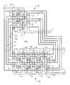
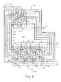
- FIG. 6is a layout view of a preferred four terminal capacitor
- FIG. 7is an exploded view of a preferred circuit assembly that incorporates multi-terminal capacitors
- FIG. 8is schematic view of a system utilizing a four terminal capacitor as a decoupling capacitor.
- FIG. 9is a schematic view of a system utilizing a four terminal capacitor as a filtering capacitor.
- FIG. 1sets forth a simplified schematic view of a preferred embodiment of the multi-terminal capacitive structure of the present invention.
- the preferred multi-terminal capacitive structureis a four-terminal capacitor 2 .
- An electrical circuit representation of the preferred structureis shown in FIG. 2 and a symbolic representation is shown in FIG. 3 .
- the four-terminal capacitor 2includes a positive input terminal 3 , a negative input terminal 4 , a positive output terminal 5 , and a negative output terminal 6 all of which are coupled to a plurality of electrodes 7 , 8 . Between the electrodes 7 , 8 is a dielectric layer (not shown).
- the preferred four-terminal capacitor 2is implemented using a multi-layer thin film capacitor structure.
- An exemplary multi-layer capacitor structure that is useful for the present inventionis shown in commonly assigned U.S. Pat. No. 5,745,335, which is incorporated herein by reference.
- the multi-terminal capacitor structure of the present inventionis much improved over the typical two-terminal capacitor structure for noise reduction applications because, among other things, the multi-terminal capacitor structure provides the ability to utilize multiple connection terminals on a given capacitor.
- two input terminals and two output terminalsare defined.
- the input terminalsprovide coupling points for the positive and common polarities of a system DC power supply
- the output terminalsprovide coupling points for a local sub-component within the system that receives DC power.
- a three terminal capacitor structurethe structure is provided with a positive input terminal, a positive output terminal, and a common negative input/output terminal.
- the structureis provided with a negative input terminal, a negative output terminal, and a common positive input/output terminal.
- the multi-terminal capacitor structureis much improved in attenuating high-frequency electrical disturbances superimposed on the DC supply which may be present at the input terminals.
- the multi-terminal capacitor structure improved attenuating abilityis achieved in large part by forcing the DC power from the DC supply that is to be supplied to the local sub-component to feed through the capacitor electrodes from the input side of the electrodes to the output side of the electrodes.
- the capacitor electrodesfunction as a form of transmission line that attenuates high-frequency energy.
- the desired noise attenuating ability of the multi-terminal capacitoris not limited by the electrical leads that are connected to the capacitor terminals as is the case with traditional two-terminal discrete capacitors.
- the noise attenuation provided by the multi-terminal capacitor structureis achievable over a much broader range of frequencies than that which is possible with a conventional two-terminal discrete capacitor.
- a greater level of attenuationcan be achieved by lengthening the distance between the input and output terminals.
- the potential increase in the DC power supply resistance caused by the lengthening of the distance between the input and output leadscan be compensated for by increasing the width of the capacitor electrodes.
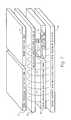
- the preferred multi-terminal capacitor structureis a multi-layer thin film distributed capacitance structure 10 .
- Structure 10includes a conventional substrate 12 (e.g. of silicon or any other suitable material) covered by an insulation layer 14 (e.g. of silicon dioxide or any other suitable insulator material).
- a bottom electrode layer 16formed of any suitable metal (e.g. nickel, platinum or palladium) is formed on top of insulation layer 14 .
- the surface area of bottom electrode layer 16is not as large as the surface area of insulation layer 14 thereby leaving a portion of the underlying insulation layer 14 exposed.
- bottom electrode layer 16Above bottom electrode layer 16 are successive pairs of intermediate electrode layers/dielectric layers 18 a , 18 b , 20 a , 20 b , and 22 a , 22 b . Above the upper intermediate layers 22 a , 22 b are top layers 24 a , 24 b (layer 24 a being an electrode layer and layer 24 b being a dielectric layer). The surface area of each successive layer is smaller than the surface area of the layer immediately underlying it thereby leaving a portion of each layer exposed.
- the layers 16 and 18 a , 18 b to 24 a , 24 bare arranged in a mesa structure.
- the pairs of layersbecome progressively larger from top to bottom so that the top surface of each lower layer pair is larger than the bottom surface of each layer above it and extends laterally beyond the layer above it in all horizontal dimensions.
- the entire structureis covered with a layer of insulation 26 (shown in FIG. 4 ), typically silicon dioxide. Since the insulation layer 26 follows the stepped pattern of the mesa, the insulation layer 26 defines a set of annular horizontal surfaces 30 , 32 , 34 , 36 , 38 , 40 , 42 , 44 , and 46 over the projecting edges of each electrode layer 16 , 18 a , 20 a , 22 a .
- Windows or viasare opened in the horizontal annular surfaces 30 to 46 and in the top horizontal surface 48 through which contacts 50 , 52 , 52 , 54 , 56 , 58 , 60 , 62 , 64 , 66 , and 68 are established (typically of gold or other suitable conductive material) to the electrodes 16 , 18 a , 20 a , 22 a , and 24 a.
- FIGS. 6Shown in FIGS. 6 is a layout drawing of a preferred four-terminal capacitor structure.
- the structureincludes a bottom electrode layer 16 , successive pairs of intermediate electrode layers 18 a , 18 b , 20 a , 20 b , and 22 a , 22 b , each of which overlie dielectric layers (not shown), and a top layers 24 a that overlies a dielectric layer (not shown).
- the surface area of each successive layeris smaller than the surface area of the layer immediately underlying it thereby leaving a portion of each layer exposed.
- Each electrode layer 16 , 18 a , 20 a , 22 a , and 24 ahas an input side 80 and an output side 90 .
- the outer periphery of the input side and output side of layers 18 a and 22 ainclude a plurality of laterally projecting surfaces 70 that extend further over the underlying layer than the remainder of the respective side portions of that layer.
- the capacitor structurealso includes a plurality of contacts 50 , 52 , 52 , 54 , 56 , 58 , 60 , 62 , 64 , 66 , and 68 in each electrode layer.
- layer 16includes two contacts 50 on the input side and four contacts 68 on the output side.
- the other layers in this embodimentinclude two contacts on the input side and four contacts on the output side.
- trace 82couples contacts 50 , 54 , and 58 to the negative input terminal 4 .
- Trace 84couples contacts 52 and 56 to the positive input terminal 3 .
- Trace 86couples contacts 62 and 66 to the positive output terminal 5 .
- trace 88couples contacts 60 , 64 , and 68 to the negative output terminal 6 .
- the outer projecting surfaces 70provide surfaces on which contacts 52 and 56 on the input side and contacts 62 and 66 on the output side can be located.
- the mesacan be of any shape, e.g. square, rectangular, round, elliptical, triangular, or L-shaped.
- a further advantage of the mesa structure with contacts at the exposed edgesis that it is not necessary to have openings through dielectric layers, which could cause defects and adhesion problems.
- each capacitive structurecan be formed independent of the other structures to have different numbers of layers and different contact coupling arrangements.
- the impedance looking into the output terminals 5 , 6can be optimized, for example, by increasing or decreasing the number of local contacts and by adjusting the width of the electrical traces 86 and 88 leading to the contacts.
- the impedance looking into the input terminals 3 , 4can be tuned to the source impedance, for example, by using the sheet resistance of the capacitor electrodes to full advantage.
- An effective termination resistance of several Ohmscan be realized by increasing the aspect ratio of the capacitor region where the connection is made.
- a long, narrow region of capacitor electrodewill introduce several squares of sheet resistance, a value which can be tuned to the equivalent source impedance looking back in the system's DC power supply.
- All of the electrode and dielectric layers shownare film layers, deposited by conventional techniques such as sputtering, chemical vapor deposition, evaporation, or spin-on techniques, all of which are well-known in the art.
- the electrode and dielectric layersare preferably thin film layers with very small thicknesses, typically in the order of 0.03 to 1.0.mu.m, although they can be thicker if desired.
- the intermediate and top electrode layersare, like the bottom electrode layer 16 , of any suitable metal such as platinum and/or palladium.
- the dielectric layersare of any desired suitable material.
- One class of materials which has been found to be particularly suitableis the class known as ferroelectric materials, also called polar dielectric materials, such as those disclosed in U.S. Pat. No.
- ferroelectric or polar dielectric materialsare lead zirconate titanate compositions.
- ferroelectric (polar) dielectric materialsexhibit spontaneous polarization at temperatures below their Curie temperature.
- Another advantage of the preferred structureis that because it is formed using thin film technology, it is highly adaptable for use in flip chip mounting.
- Flip chip mountingfurther increases the advantages of the present invention in filtering noise.
- lead lengthscan be minimized. The reduced lead lengths will result in decreased circuit inductance and resistance of a system using the present invention.
- a signal processing chip 92 and a multi-layer capacitor chip 94are mounted onto a substrate 96 that has multi-layer thick-film metal routing on both sides.
- Input DC poweris routed through the substrate 96 to the capacitor chip 94 .
- Decoupled DC poweris then routed from capacitor chip 94 to signal processing chip 92 .
- Multi-layer capacitor chip 98is provided with DC power through wire bonds 93 .
- Memory chip 95 and signal processing chip 97are flip chip mounted onto multi-layer capacitor chip 98 .
- Multi-layer capacitor chip 98provides decoupled DC power to memory chip 95 and signal processing chip 97 through contacts accessible through their top surfaces.
- Signal processing chips 92 and 97 and memory chip 95contain multiple circuit blocks, each running on different power supplies.
- the multi-layer capacitor chips 94 and 98can comprise a plurality of capacitor structures wherein each capacitor structure provides power to and electrically isolates one of the circuit blocks.
- FIG. 8An example of the use of the multi-terminal capacitor structure in a decoupling application is shown in FIG. 8 .
- System power from a DC power supply 102is provided at the input terminals 3 , 4 of the capacitor 104 and is delivered to the output terminals 4 , 5 via the low-resistance paths through the upper and lower electrodes of the capacitor structure 104 .
- the DC power supplied at the input terminals 3 , 4is potentially noisy because of the injection of noise from some other sub-component 106 of the system. By forcing the supply voltage to flow through the capacitor electrodes, high-frequency transients are attenuated by the intrinsic capacitor structure.
- the DC power available at the output terminals 4 , 5is thus a “cleaner” source for the sub-component 108 it supplies; the high-frequency noise that was originally present at the input terminals has been substantially attenuated by the capacitance.
- the impedance of the input leadsdoes not affect the attenuation transfer characteristic, which is a key advantage over two terminal capacitors.
- FIG. 9An example of the use of the multi-terminal capacitor structure in another filtering application is shown in FIG. 9.
- a low frequency signal source 110provides a signal to a sensing circuit 112 .
- Another component 114 of the systemgenerates high frequency noise that degrades the quality of the original signal.
- the original signal with the high frequency noiseis fed to the multi-terminal capacitor 116 .
- the signalflows through the capacitor electrodes from the input terminals to the output terminals.
- the capacitor 116thereby attenuates the noise and provides a cleaner signal to the sensing circuit 112 .
- Gennum's multi-layer film capacitorsare created using a photolithographic process that allows the geometry of any capacitor to be customized on an application-specific or product-specific basis. This includes the flexibility to adjust the equivalent series resistance and inductance of each physical connection. Therefore, the limitations which electrical leads impose on the high-frequency performance of capacitors can be ameliorated, for example, by increasing the width of connections to capacitor electrodes and by placing multiple physical contacts in parallel at each connection point.
- a further advantage of the technologyis the ability to independently customize the equivalent impedance looking into different pairs of terminals of the capacitor. For example, it is possible to increase the series resistance looking into the input terminals of a decoupling capacitor constructed in accordance with the present invention to minimize reflections of high-frequency disturbances present on the power supply. Similarly the output terminals of the same capacitor structure can be configured to have very low series resistance, improving the ability of the capacitor to attenuate disturbances induced on the local DC power supply lines and to prevent those disturbances from leaking out to other sub-components in the system.
- the photolithographic means by which a capacitor is createdplaces no limits on the number of terminals which can be attached to each electrode of the capacitor. Further, the layout style of the terminals can be optimized to increase the size and effectiveness of the surrounding local capacitance.
Landscapes
- Semiconductor Integrated Circuits (AREA)
- Fixed Capacitors And Capacitor Manufacturing Machines (AREA)
- Structures For Mounting Electric Components On Printed Circuit Boards (AREA)
- Piezo-Electric Or Mechanical Vibrators, Or Delay Or Filter Circuits (AREA)
- Details Of Connecting Devices For Male And Female Coupling (AREA)
Abstract
Description
Claims (24)
Priority Applications (5)
| Application Number | Priority Date | Filing Date | Title |
|---|---|---|---|
| US09/838,412US6549396B2 (en) | 2001-04-19 | 2001-04-19 | Multiple terminal capacitor structure |
| CA002381117ACA2381117C (en) | 2001-04-19 | 2002-04-10 | Improved multiple terminal capacitor structure |
| AT02008769TATE434265T1 (en) | 2001-04-19 | 2002-04-18 | CAPACITOR STRUCTURE WITH A VARIETY OF CONNECTIONS |
| EP02008769AEP1251559B1 (en) | 2001-04-19 | 2002-04-18 | Multiple terminal capacitor structure |
| DE60232619TDE60232619D1 (en) | 2001-04-19 | 2002-04-18 | Capacitor structure with a variety of connections |
Applications Claiming Priority (1)
| Application Number | Priority Date | Filing Date | Title |
|---|---|---|---|
| US09/838,412US6549396B2 (en) | 2001-04-19 | 2001-04-19 | Multiple terminal capacitor structure |
Publications (2)
| Publication Number | Publication Date |
|---|---|
| US20020163769A1 US20020163769A1 (en) | 2002-11-07 |
| US6549396B2true US6549396B2 (en) | 2003-04-15 |
Family
ID=25277033
Family Applications (1)
| Application Number | Title | Priority Date | Filing Date |
|---|---|---|---|
| US09/838,412Expired - LifetimeUS6549396B2 (en) | 2001-04-19 | 2001-04-19 | Multiple terminal capacitor structure |
Country Status (5)
| Country | Link |
|---|---|
| US (1) | US6549396B2 (en) |
| EP (1) | EP1251559B1 (en) |
| AT (1) | ATE434265T1 (en) |
| CA (1) | CA2381117C (en) |
| DE (1) | DE60232619D1 (en) |
Cited By (7)
| Publication number | Priority date | Publication date | Assignee | Title |
|---|---|---|---|---|
| US20060157792A1 (en)* | 2005-01-19 | 2006-07-20 | Kyocera Corporation | Laminated thin film capacitor and semiconductor apparatus |
| US20070187804A1 (en)* | 2005-11-04 | 2007-08-16 | Samir El Rai | Monolithic integrated circuit |
| US20080304202A1 (en)* | 2007-06-04 | 2008-12-11 | Taiyo Yuden Co., Ltd. | Multi-layer capacitor and integrated circuit module |
| US20090230446A1 (en)* | 2008-03-17 | 2009-09-17 | Technology Alliance Group, Inc. | Semiconductor device and bypass capacitor module |
| US20110191998A1 (en)* | 2007-05-01 | 2011-08-11 | Avx Corporation | Precision laser adjustable thin film capacitors |
| US20210020587A1 (en)* | 2019-06-11 | 2021-01-21 | Skyworks Solutions, Inc. | Moisture barrier for metal insulator metal capacitors and integrated circuit having the same |
| US11990470B2 (en)* | 2021-09-24 | 2024-05-21 | International Business Machines Corporation | Ferroelectric and paraelectric stack capacitors |
Families Citing this family (49)
| Publication number | Priority date | Publication date | Assignee | Title |
|---|---|---|---|---|
| US5345170A (en) | 1992-06-11 | 1994-09-06 | Cascade Microtech, Inc. | Wafer probe station having integrated guarding, Kelvin connection and shielding systems |
| US6380751B2 (en) | 1992-06-11 | 2002-04-30 | Cascade Microtech, Inc. | Wafer probe station having environment control enclosure |
| US6232789B1 (en) | 1997-05-28 | 2001-05-15 | Cascade Microtech, Inc. | Probe holder for low current measurements |
| US5561377A (en) | 1995-04-14 | 1996-10-01 | Cascade Microtech, Inc. | System for evaluating probing networks |
| US5914613A (en) | 1996-08-08 | 1999-06-22 | Cascade Microtech, Inc. | Membrane probing system with local contact scrub |
| US6002263A (en) | 1997-06-06 | 1999-12-14 | Cascade Microtech, Inc. | Probe station having inner and outer shielding |
| US6256882B1 (en) | 1998-07-14 | 2001-07-10 | Cascade Microtech, Inc. | Membrane probing system |
| US6578264B1 (en) | 1999-06-04 | 2003-06-17 | Cascade Microtech, Inc. | Method for constructing a membrane probe using a depression |
| US6445202B1 (en) | 1999-06-30 | 2002-09-03 | Cascade Microtech, Inc. | Probe station thermal chuck with shielding for capacitive current |
| US6838890B2 (en) | 2000-02-25 | 2005-01-04 | Cascade Microtech, Inc. | Membrane probing system |
| US6914423B2 (en) | 2000-09-05 | 2005-07-05 | Cascade Microtech, Inc. | Probe station |
| US6965226B2 (en) | 2000-09-05 | 2005-11-15 | Cascade Microtech, Inc. | Chuck for holding a device under test |
| DE20114544U1 (en) | 2000-12-04 | 2002-02-21 | Cascade Microtech, Inc., Beaverton, Oreg. | wafer probe |
| US7355420B2 (en) | 2001-08-21 | 2008-04-08 | Cascade Microtech, Inc. | Membrane probing system |
| US6777964B2 (en) | 2002-01-25 | 2004-08-17 | Cascade Microtech, Inc. | Probe station |
| KR100864916B1 (en) | 2002-05-23 | 2008-10-22 | 캐스케이드 마이크로테크 인코포레이티드 | Probes for Testing Devices Under Test |
| US6847219B1 (en) | 2002-11-08 | 2005-01-25 | Cascade Microtech, Inc. | Probe station with low noise characteristics |
| US6724205B1 (en) | 2002-11-13 | 2004-04-20 | Cascade Microtech, Inc. | Probe for combined signals |
| US7250779B2 (en) | 2002-11-25 | 2007-07-31 | Cascade Microtech, Inc. | Probe station with low inductance path |
| US6861856B2 (en) | 2002-12-13 | 2005-03-01 | Cascade Microtech, Inc. | Guarded tub enclosure |
| DE10260352A1 (en)* | 2002-12-20 | 2004-07-15 | Infineon Technologies Ag | Method of manufacturing a capacitor arrangement and capacitor arrangement |
| US7221172B2 (en) | 2003-05-06 | 2007-05-22 | Cascade Microtech, Inc. | Switched suspended conductor and connection |
| US7057404B2 (en) | 2003-05-23 | 2006-06-06 | Sharp Laboratories Of America, Inc. | Shielded probe for testing a device under test |
| US7492172B2 (en) | 2003-05-23 | 2009-02-17 | Cascade Microtech, Inc. | Chuck for holding a device under test |
| DE10326087B4 (en)* | 2003-06-10 | 2008-03-20 | Infineon Technologies Ag | Component with a utility structure and an auxiliary structure |
| US7250626B2 (en) | 2003-10-22 | 2007-07-31 | Cascade Microtech, Inc. | Probe testing structure |
| WO2005065258A2 (en) | 2003-12-24 | 2005-07-21 | Cascade Microtech, Inc. | Active wafer probe |
| US7187188B2 (en) | 2003-12-24 | 2007-03-06 | Cascade Microtech, Inc. | Chuck with integrated wafer support |
| WO2005121824A2 (en) | 2004-06-07 | 2005-12-22 | Cascade Microtech, Inc. | Thermal optical chuck |
| US7330041B2 (en) | 2004-06-14 | 2008-02-12 | Cascade Microtech, Inc. | Localizing a temperature of a device for testing |
| KR101157449B1 (en) | 2004-07-07 | 2012-06-22 | 캐스케이드 마이크로테크 인코포레이티드 | Probe head having a membrane suspended probe |
| EP1789812A2 (en) | 2004-09-13 | 2007-05-30 | Cascade Microtech, Inc. | Double sided probing structures |
| US7535247B2 (en) | 2005-01-31 | 2009-05-19 | Cascade Microtech, Inc. | Interface for testing semiconductors |
| US7656172B2 (en) | 2005-01-31 | 2010-02-02 | Cascade Microtech, Inc. | System for testing semiconductors |
| US20060274476A1 (en)* | 2005-04-13 | 2006-12-07 | Andrew Cervin-Lawry | Low loss thin film capacitor and methods of manufacturing the same |
| US7449899B2 (en) | 2005-06-08 | 2008-11-11 | Cascade Microtech, Inc. | Probe for high frequency signals |
| JP5080459B2 (en) | 2005-06-13 | 2012-11-21 | カスケード マイクロテック インコーポレイテッド | Wideband active / passive differential signal probe |
| US7609077B2 (en) | 2006-06-09 | 2009-10-27 | Cascade Microtech, Inc. | Differential signal probe with integral balun |
| US7764072B2 (en) | 2006-06-12 | 2010-07-27 | Cascade Microtech, Inc. | Differential signal probing system |
| US7723999B2 (en) | 2006-06-12 | 2010-05-25 | Cascade Microtech, Inc. | Calibration structures for differential signal probing |
| US7403028B2 (en) | 2006-06-12 | 2008-07-22 | Cascade Microtech, Inc. | Test structure and probe for differential signals |
| US7443186B2 (en) | 2006-06-12 | 2008-10-28 | Cascade Microtech, Inc. | On-wafer test structures for differential signals |
| WO2008041565A1 (en)* | 2006-09-27 | 2008-04-10 | Kyocera Corporation | Capacitor, capacitor device, electronic component, filter device, communication device and method for manufacturing capacitor device |
| US7876114B2 (en) | 2007-08-08 | 2011-01-25 | Cascade Microtech, Inc. | Differential waveguide probe |
| US7888957B2 (en) | 2008-10-06 | 2011-02-15 | Cascade Microtech, Inc. | Probing apparatus with impedance optimized interface |
| US8410806B2 (en) | 2008-11-21 | 2013-04-02 | Cascade Microtech, Inc. | Replaceable coupon for a probing apparatus |
| US8319503B2 (en) | 2008-11-24 | 2012-11-27 | Cascade Microtech, Inc. | Test apparatus for measuring a characteristic of a device under test |
| US20110007488A1 (en)* | 2009-07-07 | 2011-01-13 | Chin-Wei Liu | Power supply current circuit structure |
| US9648727B2 (en) | 2015-01-22 | 2017-05-09 | Harris Corporation | Fault detection optimized electronic circuit and method |
Citations (5)
| Publication number | Priority date | Publication date | Assignee | Title |
|---|---|---|---|---|
| US4916576A (en) | 1989-02-27 | 1990-04-10 | Fmtt, Inc. | Matrix capacitor |
| US5629655A (en) | 1992-10-27 | 1997-05-13 | Ericsson Inc. | Integrated distributed RC low-pass filters |
| US5910879A (en)* | 1996-06-27 | 1999-06-08 | Herbert; Edward | 3- and 4-terminal capacitors with "Faraday-shielded" connections |
| US6243253B1 (en)* | 1997-06-27 | 2001-06-05 | Avx Corporation | Surface mount multilayer capacitor |
| US6266229B1 (en)* | 1997-11-10 | 2001-07-24 | Murata Manufacturing Co., Ltd | Multilayer capacitor |
Family Cites Families (2)
| Publication number | Priority date | Publication date | Assignee | Title |
|---|---|---|---|---|
| US5745335A (en)* | 1996-06-27 | 1998-04-28 | Gennum Corporation | Multi-layer film capacitor structures and method |
| JP2000183286A (en)* | 1998-12-10 | 2000-06-30 | Nec Corp | Semiconductor integrated circuit |
- 2001
- 2001-04-19USUS09/838,412patent/US6549396B2/ennot_activeExpired - Lifetime
- 2002
- 2002-04-10CACA002381117Apatent/CA2381117C/ennot_activeExpired - Fee Related
- 2002-04-18EPEP02008769Apatent/EP1251559B1/ennot_activeExpired - Lifetime
- 2002-04-18ATAT02008769Tpatent/ATE434265T1/ennot_activeIP Right Cessation
- 2002-04-18DEDE60232619Tpatent/DE60232619D1/ennot_activeExpired - Fee Related
Patent Citations (5)
| Publication number | Priority date | Publication date | Assignee | Title |
|---|---|---|---|---|
| US4916576A (en) | 1989-02-27 | 1990-04-10 | Fmtt, Inc. | Matrix capacitor |
| US5629655A (en) | 1992-10-27 | 1997-05-13 | Ericsson Inc. | Integrated distributed RC low-pass filters |
| US5910879A (en)* | 1996-06-27 | 1999-06-08 | Herbert; Edward | 3- and 4-terminal capacitors with "Faraday-shielded" connections |
| US6243253B1 (en)* | 1997-06-27 | 2001-06-05 | Avx Corporation | Surface mount multilayer capacitor |
| US6266229B1 (en)* | 1997-11-10 | 2001-07-24 | Murata Manufacturing Co., Ltd | Multilayer capacitor |
Cited By (13)
| Publication number | Priority date | Publication date | Assignee | Title |
|---|---|---|---|---|
| US20060157792A1 (en)* | 2005-01-19 | 2006-07-20 | Kyocera Corporation | Laminated thin film capacitor and semiconductor apparatus |
| US20070187804A1 (en)* | 2005-11-04 | 2007-08-16 | Samir El Rai | Monolithic integrated circuit |
| US9437366B2 (en) | 2007-05-01 | 2016-09-06 | Avx Corporation | Method for laser adjustable thin film capacitors |
| US20110191998A1 (en)* | 2007-05-01 | 2011-08-11 | Avx Corporation | Precision laser adjustable thin film capacitors |
| US10176925B2 (en) | 2007-05-01 | 2019-01-08 | Avx Corporation | Precision laser adjustable thin film capacitors |
| US8689417B2 (en)* | 2007-05-01 | 2014-04-08 | Avx Corporation | Precision laser adjustable thin film capacitors |
| US20080304202A1 (en)* | 2007-06-04 | 2008-12-11 | Taiyo Yuden Co., Ltd. | Multi-layer capacitor and integrated circuit module |
| US20090230446A1 (en)* | 2008-03-17 | 2009-09-17 | Technology Alliance Group, Inc. | Semiconductor device and bypass capacitor module |
| US8299518B2 (en) | 2008-03-17 | 2012-10-30 | Liquid Design Systems Inc. | Semiconductor device and bypass capacitor module |
| US20210020587A1 (en)* | 2019-06-11 | 2021-01-21 | Skyworks Solutions, Inc. | Moisture barrier for metal insulator metal capacitors and integrated circuit having the same |
| US20210118821A1 (en)* | 2019-06-11 | 2021-04-22 | Skyworks Solutions, Inc. | Method of making a moisture barrier for metal insulator metal capacitors in integrated circuits |
| US12406944B2 (en)* | 2019-06-11 | 2025-09-02 | Skyworks Solutions, Inc. | Moisture barrier for metal insulator metal capacitors and integrated circuit having the same |
| US11990470B2 (en)* | 2021-09-24 | 2024-05-21 | International Business Machines Corporation | Ferroelectric and paraelectric stack capacitors |
Also Published As
| Publication number | Publication date |
|---|---|
| EP1251559A3 (en) | 2005-03-09 |
| ATE434265T1 (en) | 2009-07-15 |
| CA2381117C (en) | 2006-11-14 |
| DE60232619D1 (en) | 2009-07-30 |
| EP1251559B1 (en) | 2009-06-17 |
| EP1251559A2 (en) | 2002-10-23 |
| CA2381117A1 (en) | 2002-10-19 |
| US20020163769A1 (en) | 2002-11-07 |
Similar Documents
| Publication | Publication Date | Title |
|---|---|---|
| US6549396B2 (en) | Multiple terminal capacitor structure | |
| US6411494B1 (en) | Distributed capacitor | |
| US7339277B2 (en) | Semiconductor device having passive component and support substrate with electrodes and through electrodes passing through support substrate | |
| US7741231B2 (en) | Techniques for providing decoupling capacitance | |
| US5789807A (en) | On-chip power distribution for improved decoupling | |
| US20070267733A1 (en) | Symmetrical MIMCAP capacitor design | |
| RU2158992C2 (en) | Connection structure of elements of high- frequency microchips | |
| EP1362377A2 (en) | Multilayer capacitor structure having an array of concentric ring-shaped plates for deep sub-micron cmos | |
| US7986532B2 (en) | Split thin film capacitor for multiple voltages | |
| JP2002532903A (en) | Integrated circuit having a capacitive element | |
| EP1470588A2 (en) | Split-gate power module and method for suppressing oscillation therein | |
| US7868393B2 (en) | Space efficient integrated circuit with passive devices | |
| CN1312949C (en) | Mobile telephone set | |
| US8975725B2 (en) | Bias circuit and method of manufacturing the same | |
| US6300677B1 (en) | Electronic assembly having improved power supply bus voltage integrity | |
| US20210304964A1 (en) | Capacitor | |
| JP2638544B2 (en) | Semiconductor integrated circuit | |
| JPH08298307A (en) | Semiconductor device | |
| JPH0653414A (en) | Microwave integrated circuit | |
| US6867474B2 (en) | Monolithic circuit inductance | |
| HK1229065B (en) | Split thin film capacitor for multiple voltages |
Legal Events
| Date | Code | Title | Description |
|---|---|---|---|
| AS | Assignment | Owner name:GENNUM CORPORATION, CANADA Free format text:ASSIGNMENT OF ASSIGNORS INTEREST;ASSIGNOR:BROWN, DAVID RICHARD;REEL/FRAME:012068/0193 Effective date:20010503 | |
| STCF | Information on status: patent grant | Free format text:PATENTED CASE | |
| FPAY | Fee payment | Year of fee payment:4 | |
| AS | Assignment | Owner name:PARATEK MICROWAVE, INC., NEW HAMPSHIRE Free format text:ASSIGNMENT OF ASSIGNORS INTEREST;ASSIGNOR:GENNUM CORPORATION;REEL/FRAME:022343/0813 Effective date:20090304 | |
| FEPP | Fee payment procedure | Free format text:PAT HOLDER CLAIMS SMALL ENTITY STATUS, ENTITY STATUS SET TO SMALL (ORIGINAL EVENT CODE: LTOS); ENTITY STATUS OF PATENT OWNER: LARGE ENTITY | |
| FPAY | Fee payment | Year of fee payment:8 | |
| SULP | Surcharge for late payment | Year of fee payment:7 | |
| FEPP | Fee payment procedure | Free format text:PAT HOLDER NO LONGER CLAIMS SMALL ENTITY STATUS, ENTITY STATUS SET TO UNDISCOUNTED (ORIGINAL EVENT CODE: STOL); ENTITY STATUS OF PATENT OWNER: LARGE ENTITY | |
| AS | Assignment | Owner name:RESEARCH IN MOTION RF, INC., DELAWARE Free format text:CHANGE OF NAME;ASSIGNOR:PARATEK MICROWAVE, INC.;REEL/FRAME:028686/0432 Effective date:20120608 | |
| SULP | Surcharge for late payment | ||
| AS | Assignment | Owner name:BLACKBERRY LIMITED, ONTARIO Free format text:ASSIGNMENT OF ASSIGNORS INTEREST;ASSIGNOR:RESEARCH IN MOTION CORPORATION;REEL/FRAME:030909/0933 Effective date:20130710 Owner name:RESEARCH IN MOTION CORPORATION, DELAWARE Free format text:ASSIGNMENT OF ASSIGNORS INTEREST;ASSIGNOR:RESEARCH IN MOTION RF, INC.;REEL/FRAME:030909/0908 Effective date:20130709 | |
| FPAY | Fee payment | Year of fee payment:12 | |
| AS | Assignment | Owner name:NXP USA, INC., TEXAS Free format text:ASSIGNMENT OF ASSIGNORS INTEREST;ASSIGNOR:BLACKBERRY LIMITED;REEL/FRAME:052095/0443 Effective date:20200228 |