US6549234B1 - Pixel structure of active pixel sensor (APS) with electronic shutter function - Google Patents
Pixel structure of active pixel sensor (APS) with electronic shutter functionDownload PDFInfo
- Publication number
- US6549234B1 US6549234B1US09/170,105US17010598AUS6549234B1US 6549234 B1US6549234 B1US 6549234B1US 17010598 AUS17010598 AUS 17010598AUS 6549234 B1US6549234 B1US 6549234B1
- Authority
- US
- United States
- Prior art keywords
- pixel
- nmos transistor
- reset
- source
- pixel sensor
- Prior art date
- Legal status (The legal status is an assumption and is not a legal conclusion. Google has not performed a legal analysis and makes no representation as to the accuracy of the status listed.)
- Expired - Fee Related
Links
Images


Classifications
- H—ELECTRICITY
- H10—SEMICONDUCTOR DEVICES; ELECTRIC SOLID-STATE DEVICES NOT OTHERWISE PROVIDED FOR
- H10F—INORGANIC SEMICONDUCTOR DEVICES SENSITIVE TO INFRARED RADIATION, LIGHT, ELECTROMAGNETIC RADIATION OF SHORTER WAVELENGTH OR CORPUSCULAR RADIATION
- H10F39/00—Integrated devices, or assemblies of multiple devices, comprising at least one element covered by group H10F30/00, e.g. radiation detectors comprising photodiode arrays
- H10F39/10—Integrated devices
- H10F39/12—Image sensors
- H—ELECTRICITY
- H04—ELECTRIC COMMUNICATION TECHNIQUE
- H04N—PICTORIAL COMMUNICATION, e.g. TELEVISION
- H04N25/00—Circuitry of solid-state image sensors [SSIS]; Control thereof
- H04N25/50—Control of the SSIS exposure
- H04N25/53—Control of the integration time
- H04N25/531—Control of the integration time by controlling rolling shutters in CMOS SSIS
- H—ELECTRICITY
- H04—ELECTRIC COMMUNICATION TECHNIQUE
- H04N—PICTORIAL COMMUNICATION, e.g. TELEVISION
- H04N25/00—Circuitry of solid-state image sensors [SSIS]; Control thereof
- H04N25/70—SSIS architectures; Circuits associated therewith
- H04N25/76—Addressed sensors, e.g. MOS or CMOS sensors
- H—ELECTRICITY
- H04—ELECTRIC COMMUNICATION TECHNIQUE
- H04N—PICTORIAL COMMUNICATION, e.g. TELEVISION
- H04N25/00—Circuitry of solid-state image sensors [SSIS]; Control thereof
- H04N25/70—SSIS architectures; Circuits associated therewith
- H04N25/76—Addressed sensors, e.g. MOS or CMOS sensors
- H04N25/77—Pixel circuitry, e.g. memories, A/D converters, pixel amplifiers, shared circuits or shared components
Definitions
- the present inventionis directed to a pixel (picture element) structure of an active pixel sensor (APS), and in particular to a pixel structure of an active pixel sensor (APS) which can carry out a reset operation by pixel units by providing the pixels with a double reset structure to implement an electronic shutter function.
- APSactive pixel sensor
- CMOS sensorsthe most successful pixel structure in processing noise is a pixel structure using an active pixel sensor (APS).
- a remarkable characteristic of the pixel structure using the active pixel sensor (APS)is that each pixel amplifies the image information accumulated in a photo-diode, namely, the charge caused by photoelectrons, before converting it into a voltage.
- FIG. 1is a block diagram illustrating a conventional pixel structure using an active pixel sensor (APS).
- the conventional pixel structureincludes: a plurality of pixels P 11 -Pmn arrayed in a lattice pattern of rows and columns; a row selection decoder 1 selectively outputting a row selection signal ROW to the plurality of pixels P 11 -Pmn; a first line counter LC 1 counting a number of lines of the pixels selected by the row selection decoder 1 ; a reset selection decoder 2 selectively outputting a reset signal RS to each row of pixels; a second line counter LC 2 counting a number of lines of the pixels selected by the reset selection decoder 2 ; a column reading unit 3 reading image information stored in the pixels; and a pixel counter PC 1 counting a number of the pixels read by the column reading unit 3 .
- FIG. 2is a circuit diagram illustrating a pixel PXji located in a predetermined position.
- the pixel PXjiincludes: a first NMOS transistor NM 21 with its gate receiving the reset signal RS and its drain receiving a power supply voltage VDD; a photo-diode PD with its anode connected to ground and its cathode connected to the source of the first NMOS transistor NM 21 ; a second NMOS transistor NM 22 with its gate commonly connected to the source of the first NMOS transistor NM 21 and the cathode of the photo-diode PD, and with its drain receiving the power supply voltage VDD; and a third NMOS transistor NM 23 with its gate receiving the row selection signal ROW, its drain connected to the source of the second NMOS transistor NM 22 , and its source outputting an output signal OUT.
- the reset signal RS outputted from the reset selection decoder 2is inputted to the gate of the first NMOS transistor NM 21 of a selected pixel PXji which is located in a predetermined position, and thus the first NMOS transistor NM 21 is turned on.
- the first NMOS transistor NM 21discharges photoelectrons generated by incident light, thereby draining any internal electrical charge from the photo-diode PD.
- the reset operationis carried out in line units.
- the voltage produced by accumulated photoelectronsis amplified by the second NMOS transistor NM 22 .
- the row selection signal ROW outputted from the row selection decoder 1is applied to the gate of the third NMOS transistor NM 23 , and thus the third NMOS transistor NM 23 is turned on. Accordingly, the output signal OUT is outputted from the source of the third NMOS transistor NM 23 to the column reading unit 3 .
- the output signal OUTrepresents the output image information of the selected pixel PXji.
- the term “information”refers to the second image property, typically the light intensity, that is, the photonic energy incident on the photo-diode in each pixel sensor, which causes the accumulation of electrical charge (i.e., electron-hole pairs generated in a semiconductor junction) and in terms of an induced voltage potential due to photo-electrons producing a current.
- the conventional pixel structure of the active pixel sensorhas a disadvantage in that, as the reset operation is carried out not in pixel units but in line units, an electronic shutter function cannot be utilized.
- APSactive pixel sensor
- a pixel structure of an active pixel sensor (APS) with an electronic shutter functionincluding: a plurality of pixel sensors arrayed in rows and columns; a row selection decoder outputting a row selection signal ROW to each pixel sensor; a first line counter counting a number of lines of the pixels selected by the row selection decoder; a line reset selection decoder outputting a line reset signal to each pixel sensor; a second line counter counting a number of lines of the pixel selected by the line reset selection decoder; a column reset selection decoder outputting a column reset signal to each pixel sensor; a first pixel counter counting a number of the pixels selected by the column reset selection decoder; a column reading unit reading image information stored in the pixels; and a second pixel counter counting a number of the pixels which are read by the column reading unit.
- APSactive pixel sensor
- FIG. 1is a block diagram illustrating a conventional pixel structure of an image sensor using an active pixel sensor (APS);
- FIG. 2is a circuit diagram illustrating a general pixel in the conventional pixel structure using the active pixel sensor (APS) in FIG. 1;
- FIG. 3is a block diagram illustrating a pixel structure of an image sensor with an electronic shutter function using an active pixel sensor (APS) in accordance with the present invention
- FIG. 4is a circuit diagram illustrating a pixel in the pixel sensor structure with the electronic shutter function using the active pixel sensor (APS) in FIG. 3 in accordance with a first preferred embodiment of the present invention.
- FIG. 5is a circuit diagram illustrating a pixel in the pixel sensor structure with the electronic shutter function using the active pixel sensor (APS) in FIG. 3 in accordance with a second preferred embodiment of the present invention.
- APSactive pixel sensor
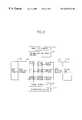
- FIG. 3is a block diagram illustrating a pixel sensor array structure with an electronic shutter function using an active pixel sensor (APS) in accordance with the present invention.
- the pixel sensor array structure with the electronic shutter function using the active pixel sensorincludes: a plurality of pixels PX 11 -PXmn which are arrayed in a lattice pattern of rows and columns and sense image information; a row selection decoder 10 outputting a row selection signal ROW to output the image information, i.e., charge, stored in each pixel PX 11 -PXmn; a first line counter LC 31 counting a number of lines of the pixel selected by the row selection decoder 10 ; a line reset selection decoder 20 outputting a line reset signal LRS to reset each pixel PX 11 -PXmn in line units; a second line counter LC 32 counting a number of lines selected by the line reset selection decoder 20 ; a column reset selection decoder 30 outputting a column reset signal C
- an electrical charge accumulating time of the pixel PXji located in a predetermined positionis T(ji).
- T(ji)an electrical charge accumulating time of the pixel PXji located in a predetermined position.
- the value of T(ji)is identical to a field or frame constituting time.
- Each pixelhas an identical photoelectron accumulating time.
- the electric charge accumulating time T(ji) of the pixel PXji located in a predetermined positionis the time after the reset operation of the pixel PXji before an output of the charge generated by the photoelectrons accumulated in the photo-diode PD, namely, from the time when the pixel is reset to the time when the output signal OUT is outputted by application of the row selection signal ROW.
- the electrical charge accumulating time Tis represented by the following equation
- ndenotes the number of the rows
- mdenotes the number of the columns, respectively.
- the electrical charge accumulating time of the pixel PXji located in a predetermined positionis T(ji).
- the photo-diode PDIn order to read the image information, i.e., charge, accumulated in the pixel PXji, namely, charge caused by the photoelectrons, the photo-diode PD should be reset and initialized at least before the electron accumulating time T(ji). Therefore, the certain electron accumulating time T is provided in pixel units, and thus the electronic shutter function can be employed.
- a time difference which corresponds to the position of the pixelsnamely, the number of the rows (n) and the number of the columns (m) is generated among the pixels PX 11 -PXmn. Therefore, the time difference between a first transmitted pixel charge and a last transmitted pixel charge in a frame corresponds to one frame or one field. Therefore, an initialization can be carried out in pixel units by controlling the reset operation in row and column units, thereby discriminately providing an electronic shutter timing to each pixel PX 11 -PXmn.
- FIG. 4is a circuit diagram illustrating a pixel PXji located in a predetermined position in accordance with a first preferred embodiment of the present invention.
- the pixelincludes: a first NMOS transistor NM 41 with its gate and drain connected to each other and receiving a power voltage supply VDD; a second NMOS transistor NM 42 with its gate receiving the line reset signal LRS and its drain connected to the source of the first NMOS transistor NM 41 ; a third NMOS transistor NM 43 with its gate receiving the column reset signal CRS, its drain connected to a source of the second NMOS transistor NM 42 , and its source connected to a ground; a fourth NMOS transistor NM 44 with its gate connected to the source of the first NMOS transistor NM 41 and the drain of the second NMOS transistor NM 42 at the same time, and its drain receiving the power supply voltage VDD; a photo-diode PD with its anode connected to a ground voltage VSS and its cathode connected to the
- the row selection signal ROWis inputted to the gate of the sixth NMOS transistor NM 46 , and thus the sixth NMOS transistor NM 46 is turned on. At this time, the output signal OUT is outputted from the source of the sixth NMOS transistor NM 46 .
- FIG. 5is a circuit diagram illustrating a pixel sensor PXji located in a predetermined position in a pixel sensor structure with an electron shutter function using an active pixel sensor (APS) in accordance with a second preferred embodiment of the present invention.
- the pixel sensorincludes: a first NMOS transistor NM 51 with its gate receiving the line reset signal LRS and its drain receiving the power supply voltage VDD; a second NMOS transistor NM 52 with its gate receiving the column reset signal CRS and its drain connected to the source of the first NMOS transistor NM 51 ; a photo-diode PD with its anode connected to ground voltage VSS and with its cathode connected to the source of the second NMOS transistor NM 52 ; a third NMOS transistor NM 53 with its gate commonly connected to the source of the second NMOS transistor NM 52 and to the cathode of the photo-diode PD, and with its drain receiving the power supply voltage VDD; and a fourth NMOS transistor NM 54
- the row selection signal ROWis inputted to the gate of the NMOS transistor NM 43 , and thus the fourth NMOS transistor NM 54 is turned on, and the output signal OUT is outputted from the source of the fourth NMOS transistor NM 54 .
- the pixelsare reset in column and row units, and thus each pixel sensor is initialized when the reset signals for the column and row are simultaneously applied thereto. Accordingly, it makes it possible to carry out the initialization in pixel units, and thus the electronic shutter function appropriate for a movie camera can be provided.
Landscapes
- Engineering & Computer Science (AREA)
- Multimedia (AREA)
- Signal Processing (AREA)
- Transforming Light Signals Into Electric Signals (AREA)
- Solid State Image Pick-Up Elements (AREA)
- Facsimile Heads (AREA)
Abstract
Description
Claims (3)
Applications Claiming Priority (2)
| Application Number | Priority Date | Filing Date | Title |
|---|---|---|---|
| KR98-21259 | 1998-06-09 | ||
| KR1019980021259AKR100280488B1 (en) | 1998-06-09 | 1998-06-09 | Active pixel sensor type pixel structure with electronic shutter function |
Publications (1)
| Publication Number | Publication Date |
|---|---|
| US6549234B1true US6549234B1 (en) | 2003-04-15 |
Family
ID=19538713
Family Applications (1)
| Application Number | Title | Priority Date | Filing Date |
|---|---|---|---|
| US09/170,105Expired - Fee RelatedUS6549234B1 (en) | 1998-06-09 | 1998-10-13 | Pixel structure of active pixel sensor (APS) with electronic shutter function |
Country Status (5)
| Country | Link |
|---|---|
| US (1) | US6549234B1 (en) |
| JP (1) | JP2000023042A (en) |
| KR (1) | KR100280488B1 (en) |
| DE (1) | DE19852870B4 (en) |
| GB (1) | GB2338365B (en) |
Cited By (16)
| Publication number | Priority date | Publication date | Assignee | Title |
|---|---|---|---|---|
| US20020012057A1 (en)* | 2000-05-26 | 2002-01-31 | Hajime Kimura | MOS sensor and drive method thereof |
| US20020113886A1 (en)* | 2001-02-20 | 2002-08-22 | Jaroslav Hynecek | High Dynamic Range Active Pixel CMOS Image Sensor and data processing system incorporating adaptive pixel reset |
| US20030011695A1 (en)* | 2001-06-19 | 2003-01-16 | Alex Roustaei | Method and apparatus for controlling power consumption in an active pixel sensor array |
| US20030164889A1 (en)* | 2000-09-27 | 2003-09-04 | Yukio Koyanagi | Solid-state imaging device and correlated double sampling circuit |
| US6933973B1 (en)* | 1999-03-01 | 2005-08-23 | Kawasaki Microelectronics, Inc. | CMOS image sensor having block scanning capability |
| US20050265714A1 (en)* | 2004-05-28 | 2005-12-01 | Per Rosdahl | Digital shutter |
| US7068315B1 (en)* | 1999-07-12 | 2006-06-27 | Sony Corporation | Solid-state imaging device, its driving method, and camera system |
| US20060261246A1 (en)* | 2005-05-18 | 2006-11-23 | Alexander Krymski | Pixel circuit for image sensor |
| US7142240B1 (en)* | 2000-07-17 | 2006-11-28 | Psion Teklogix Systems, Inc. | Active pixel sensor array reset |
| US20090101914A1 (en)* | 2006-05-11 | 2009-04-23 | Fusayoshi Hirotsu | Semiconductor Image Sensing Device |
| US20110102623A1 (en)* | 2009-11-02 | 2011-05-05 | Sony Corporation | Solid-state imaging device and camera system |
| US20110145141A1 (en)* | 2009-10-02 | 2011-06-16 | James Blain | Method and apparatus for recharging electric vehicles |
| US9177987B2 (en) | 2012-10-12 | 2015-11-03 | Samsung Electronics Co., Ltd. | Binary CMOS image sensors, methods of operating same, and image processing systems including same |
| WO2019043446A1 (en) | 2017-09-04 | 2019-03-07 | Nng Software Developing And Commercial Llc | A method and apparatus for collecting and using sensor data from a vehicle |
| US10868867B2 (en) | 2012-01-09 | 2020-12-15 | May Patents Ltd. | System and method for server based control |
| US11290708B2 (en) | 2019-02-19 | 2022-03-29 | Edgy Bees Ltd. | Estimating real-time delay of a video data stream |
Families Citing this family (5)
| Publication number | Priority date | Publication date | Assignee | Title |
|---|---|---|---|---|
| KR100719516B1 (en)* | 2006-01-27 | 2007-05-18 | 주식회사 아펙스 | Leisure Scaffolding |
| KR100732620B1 (en)* | 2006-01-27 | 2007-06-27 | 주식회사 아펙스 | Footboard body of the footboard for leisure vehicle |
| KR100761914B1 (en)* | 2006-06-10 | 2007-09-28 | 김문건 | Car Side Step |
| KR101623960B1 (en) | 2009-06-04 | 2016-05-25 | 삼성전자주식회사 | Optoelectronic shutter, method of operating the same and optical apparatus employing the optoelectronic shutter |
| JP5578915B2 (en) | 2010-04-01 | 2014-08-27 | キヤノン株式会社 | Solid-state imaging device and driving method thereof |
Citations (19)
| Publication number | Priority date | Publication date | Assignee | Title |
|---|---|---|---|---|
| JPS5930376A (en) | 1982-08-13 | 1984-02-17 | Olympus Optical Co Ltd | solid-state imaging device |
| JPS6022879A (en) | 1983-07-19 | 1985-02-05 | Nippon Hoso Kyokai <Nhk> | System for controlling sensitivity of solid-state image pickup device |
| JPS61214870A (en) | 1985-03-20 | 1986-09-24 | Mitsubishi Electric Corp | Solid-state image pickup device |
| JPS6378679A (en) | 1986-09-22 | 1988-04-08 | Hitachi Ltd | Image pickup device |
| JPS63127679A (en) | 1986-11-18 | 1988-05-31 | Canon Inc | solid-state imaging device |
| JPH02171088A (en) | 1988-12-24 | 1990-07-02 | Sony Corp | Solid-state image pickup element |
| JPH04373272A (en) | 1991-06-21 | 1992-12-25 | Fujitsu General Ltd | MUSE signal sub-screen display circuit |
| JPH0575931A (en) | 1991-09-13 | 1993-03-26 | Canon Inc | Image pickup device |
| JPH05130519A (en) | 1991-11-05 | 1993-05-25 | Canon Inc | Solid-state imaging device |
| JPH05227489A (en) | 1992-02-14 | 1993-09-03 | Sony Corp | Solid state image pickup device |
| US5471515A (en) | 1994-01-28 | 1995-11-28 | California Institute Of Technology | Active pixel sensor with intra-pixel charge transfer |
| US5680151A (en)* | 1990-06-12 | 1997-10-21 | Radius Inc. | Method and apparatus for transmitting video, data over a computer bus using block transfers |
| US5812191A (en)* | 1994-06-01 | 1998-09-22 | Simage Oy | Semiconductor high-energy radiation imaging device |
| US5877715A (en)* | 1997-06-12 | 1999-03-02 | International Business Machines Corporation | Correlated double sampling with up/down counter |
| US5892541A (en)* | 1996-09-10 | 1999-04-06 | Foveonics, Inc. | Imaging system and method for increasing the dynamic range of an array of active pixel sensor cells |
| US6037979A (en)* | 1994-01-31 | 2000-03-14 | Sony Corporation | Solid-state imaging device having a reset switch for resetting potential of capacitor and vertical signal line |
| US6115066A (en)* | 1997-06-12 | 2000-09-05 | International Business Machines Corporation | Image sensor with direct digital correlated sampling |
| US6175383B1 (en)* | 1996-11-07 | 2001-01-16 | California Institute Of Technology | Method and apparatus of high dynamic range image sensor with individual pixel reset |
| US6344877B1 (en)* | 1997-06-12 | 2002-02-05 | International Business Machines Corporation | Image sensor with dummy pixel or dummy pixel array |
Family Cites Families (1)
| Publication number | Priority date | Publication date | Assignee | Title |
|---|---|---|---|---|
| AU1833597A (en)* | 1996-01-22 | 1997-08-22 | California Institute Of Technology | Active pixel sensor array with electronic shuttering |
- 1998
- 1998-06-09KRKR1019980021259Apatent/KR100280488B1/ennot_activeExpired - Fee Related
- 1998-10-13USUS09/170,105patent/US6549234B1/ennot_activeExpired - Fee Related
- 1998-11-03GBGB9824043Apatent/GB2338365B/ennot_activeExpired - Fee Related
- 1998-11-12JPJP10321861Apatent/JP2000023042A/enactivePending
- 1998-11-16DEDE19852870Apatent/DE19852870B4/ennot_activeExpired - Fee Related
Patent Citations (19)
| Publication number | Priority date | Publication date | Assignee | Title |
|---|---|---|---|---|
| JPS5930376A (en) | 1982-08-13 | 1984-02-17 | Olympus Optical Co Ltd | solid-state imaging device |
| JPS6022879A (en) | 1983-07-19 | 1985-02-05 | Nippon Hoso Kyokai <Nhk> | System for controlling sensitivity of solid-state image pickup device |
| JPS61214870A (en) | 1985-03-20 | 1986-09-24 | Mitsubishi Electric Corp | Solid-state image pickup device |
| JPS6378679A (en) | 1986-09-22 | 1988-04-08 | Hitachi Ltd | Image pickup device |
| JPS63127679A (en) | 1986-11-18 | 1988-05-31 | Canon Inc | solid-state imaging device |
| JPH02171088A (en) | 1988-12-24 | 1990-07-02 | Sony Corp | Solid-state image pickup element |
| US5680151A (en)* | 1990-06-12 | 1997-10-21 | Radius Inc. | Method and apparatus for transmitting video, data over a computer bus using block transfers |
| JPH04373272A (en) | 1991-06-21 | 1992-12-25 | Fujitsu General Ltd | MUSE signal sub-screen display circuit |
| JPH0575931A (en) | 1991-09-13 | 1993-03-26 | Canon Inc | Image pickup device |
| JPH05130519A (en) | 1991-11-05 | 1993-05-25 | Canon Inc | Solid-state imaging device |
| JPH05227489A (en) | 1992-02-14 | 1993-09-03 | Sony Corp | Solid state image pickup device |
| US5471515A (en) | 1994-01-28 | 1995-11-28 | California Institute Of Technology | Active pixel sensor with intra-pixel charge transfer |
| US6037979A (en)* | 1994-01-31 | 2000-03-14 | Sony Corporation | Solid-state imaging device having a reset switch for resetting potential of capacitor and vertical signal line |
| US5812191A (en)* | 1994-06-01 | 1998-09-22 | Simage Oy | Semiconductor high-energy radiation imaging device |
| US5892541A (en)* | 1996-09-10 | 1999-04-06 | Foveonics, Inc. | Imaging system and method for increasing the dynamic range of an array of active pixel sensor cells |
| US6175383B1 (en)* | 1996-11-07 | 2001-01-16 | California Institute Of Technology | Method and apparatus of high dynamic range image sensor with individual pixel reset |
| US5877715A (en)* | 1997-06-12 | 1999-03-02 | International Business Machines Corporation | Correlated double sampling with up/down counter |
| US6115066A (en)* | 1997-06-12 | 2000-09-05 | International Business Machines Corporation | Image sensor with direct digital correlated sampling |
| US6344877B1 (en)* | 1997-06-12 | 2002-02-05 | International Business Machines Corporation | Image sensor with dummy pixel or dummy pixel array |
Cited By (46)
| Publication number | Priority date | Publication date | Assignee | Title |
|---|---|---|---|---|
| US6933973B1 (en)* | 1999-03-01 | 2005-08-23 | Kawasaki Microelectronics, Inc. | CMOS image sensor having block scanning capability |
| US7068315B1 (en)* | 1999-07-12 | 2006-06-27 | Sony Corporation | Solid-state imaging device, its driving method, and camera system |
| US7224391B2 (en)* | 2000-05-26 | 2007-05-29 | Semiconductor Energy Laboratory Co., Ltd. | MOS sensor and drive method thereof |
| US7787039B2 (en) | 2000-05-26 | 2010-08-31 | Semiconductor Energy Laboratory Co., Ltd. | MOS sensor and drive method thereof |
| US8164652B2 (en) | 2000-05-26 | 2012-04-24 | Semiconductor Energy Laboratory Co., Ltd. | MOS sensor and drive method thereof |
| US20020012057A1 (en)* | 2000-05-26 | 2002-01-31 | Hajime Kimura | MOS sensor and drive method thereof |
| US7142240B1 (en)* | 2000-07-17 | 2006-11-28 | Psion Teklogix Systems, Inc. | Active pixel sensor array reset |
| US7929034B2 (en) | 2000-07-17 | 2011-04-19 | Harusaki Technologies, Llc | Active pixel sensor array reset |
| US20070091192A1 (en)* | 2000-07-17 | 2007-04-26 | Paul Hua | Active pixel sensor array reset |
| US20030164889A1 (en)* | 2000-09-27 | 2003-09-04 | Yukio Koyanagi | Solid-state imaging device and correlated double sampling circuit |
| US7079178B2 (en)* | 2001-02-20 | 2006-07-18 | Jaroslav Hynecek | High dynamic range active pixel CMOS image sensor and data processing system incorporating adaptive pixel reset |
| US20020113886A1 (en)* | 2001-02-20 | 2002-08-22 | Jaroslav Hynecek | High Dynamic Range Active Pixel CMOS Image Sensor and data processing system incorporating adaptive pixel reset |
| US20030011695A1 (en)* | 2001-06-19 | 2003-01-16 | Alex Roustaei | Method and apparatus for controlling power consumption in an active pixel sensor array |
| US20050265714A1 (en)* | 2004-05-28 | 2005-12-01 | Per Rosdahl | Digital shutter |
| US7205522B2 (en) | 2005-05-18 | 2007-04-17 | Alexander Krymski D. B. A Alexima | Pixel circuit for image sensor |
| US20060261246A1 (en)* | 2005-05-18 | 2006-11-23 | Alexander Krymski | Pixel circuit for image sensor |
| US20090101914A1 (en)* | 2006-05-11 | 2009-04-23 | Fusayoshi Hirotsu | Semiconductor Image Sensing Device |
| US20110145141A1 (en)* | 2009-10-02 | 2011-06-16 | James Blain | Method and apparatus for recharging electric vehicles |
| US20110102623A1 (en)* | 2009-11-02 | 2011-05-05 | Sony Corporation | Solid-state imaging device and camera system |
| US8610809B2 (en)* | 2009-11-02 | 2013-12-17 | Sony Corporation | Solid-state imaging device and camera system that controls a unit of plural rows |
| US11349925B2 (en) | 2012-01-03 | 2022-05-31 | May Patents Ltd. | System and method for server based control |
| US10868867B2 (en) | 2012-01-09 | 2020-12-15 | May Patents Ltd. | System and method for server based control |
| US11979461B2 (en) | 2012-01-09 | 2024-05-07 | May Patents Ltd. | System and method for server based control |
| US11128710B2 (en) | 2012-01-09 | 2021-09-21 | May Patents Ltd. | System and method for server-based control |
| US11190590B2 (en) | 2012-01-09 | 2021-11-30 | May Patents Ltd. | System and method for server based control |
| US11240311B2 (en) | 2012-01-09 | 2022-02-01 | May Patents Ltd. | System and method for server based control |
| US11245765B2 (en) | 2012-01-09 | 2022-02-08 | May Patents Ltd. | System and method for server based control |
| US12401721B1 (en) | 2012-01-09 | 2025-08-26 | May Patents Ltd. | System and method for server based control |
| US11336726B2 (en) | 2012-01-09 | 2022-05-17 | May Patents Ltd. | System and method for server based control |
| US12401720B1 (en) | 2012-01-09 | 2025-08-26 | May Patents Ltd. | System and method for server based control |
| US11375018B2 (en) | 2012-01-09 | 2022-06-28 | May Patents Ltd. | System and method for server based control |
| US12316706B2 (en) | 2012-01-09 | 2025-05-27 | May Patents Ltd. | System and method for server based control |
| US11824933B2 (en) | 2012-01-09 | 2023-11-21 | May Patents Ltd. | System and method for server based control |
| US12231497B2 (en) | 2012-01-09 | 2025-02-18 | May Patents Ltd. | Controlled AC power plug with a sensor |
| US12192283B2 (en) | 2012-01-09 | 2025-01-07 | May Patents Ltd. | System and method for server based control |
| US12010174B2 (en) | 2012-01-09 | 2024-06-11 | May Patents Ltd. | System and method for server based control |
| US12081620B2 (en) | 2012-01-09 | 2024-09-03 | May Patents Ltd. | System and method for server based control |
| US12088670B2 (en) | 2012-01-09 | 2024-09-10 | May Patents Ltd. | System and method for server based control |
| US12137144B2 (en) | 2012-01-09 | 2024-11-05 | May Patents Ltd. | System and method for server based control |
| US12149589B2 (en) | 2012-01-09 | 2024-11-19 | May Patents Ltd. | Controlled AC power plug with an actuator |
| US12177301B2 (en) | 2012-01-09 | 2024-12-24 | May Patents Ltd. | System and method for server based control |
| US9177987B2 (en) | 2012-10-12 | 2015-11-03 | Samsung Electronics Co., Ltd. | Binary CMOS image sensors, methods of operating same, and image processing systems including same |
| WO2019043446A1 (en) | 2017-09-04 | 2019-03-07 | Nng Software Developing And Commercial Llc | A method and apparatus for collecting and using sensor data from a vehicle |
| US11849105B2 (en) | 2019-02-19 | 2023-12-19 | Edgy Bees Ltd. | Estimating real-time delay of a video data stream |
| US11563932B2 (en) | 2019-02-19 | 2023-01-24 | Edgy Bees Ltd. | Estimating real-time delay of a video data stream |
| US11290708B2 (en) | 2019-02-19 | 2022-03-29 | Edgy Bees Ltd. | Estimating real-time delay of a video data stream |
Also Published As
| Publication number | Publication date |
|---|---|
| DE19852870B4 (en) | 2005-10-20 |
| GB2338365A (en) | 1999-12-15 |
| KR20000001150A (en) | 2000-01-15 |
| JP2000023042A (en) | 2000-01-21 |
| GB9824043D0 (en) | 1998-12-30 |
| KR100280488B1 (en) | 2001-02-01 |
| DE19852870A1 (en) | 1999-12-16 |
| GB2338365B (en) | 2000-04-26 |
Similar Documents
| Publication | Publication Date | Title |
|---|---|---|
| US6549234B1 (en) | Pixel structure of active pixel sensor (APS) with electronic shutter function | |
| US9445020B2 (en) | Solid-state imaging element having image signal overflow path | |
| US7821556B2 (en) | Amplifying solid-state imaging device, and method for driving the same | |
| JP3031367B1 (en) | Image sensor | |
| KR100279295B1 (en) | Active pixel sensor | |
| KR20010032108A (en) | Intra-pixel frame storage element, array, and electronic shutter method suitable for electronic still camera applications | |
| EP3627556B1 (en) | Solid-state image sensor and image-capturing device | |
| US20080315272A1 (en) | Image sensor with gain control | |
| JP2000004399A (en) | Solid-state imaging device and driving method thereof | |
| TW202215838A (en) | Image sensor with configurable pixel circuit and method | |
| US7068315B1 (en) | Solid-state imaging device, its driving method, and camera system | |
| US20090078975A1 (en) | CMOS image sensor | |
| JP3578648B2 (en) | Amplification type solid-state imaging device and driving method thereof | |
| KR101064495B1 (en) | Wide dynamic range image sensor and its operation method | |
| JP2013187233A (en) | Solid-state imaging device, driving method thereof and electronic apparatus | |
| JP2001119628A (en) | Solid-state image-pickup element | |
| JP2005184864A (en) | Solid-state imaging device | |
| JPS59117377A (en) | Solid-state image pickup element |
Legal Events
| Date | Code | Title | Description |
|---|---|---|---|
| AS | Assignment | Owner name:LG SEMICON CO., LTD., KOREA, REPUBLIC OF Free format text:ASSIGNMENT OF ASSIGNORS INTEREST;ASSIGNOR:LEE, SUNG-MIN;REEL/FRAME:009517/0596 Effective date:19980928 | |
| AS | Assignment | Owner name:HYUNDAI ELECTRONICS INDUSTRIES, CO., LTD., KOREA, Free format text:MERGER;ASSIGNOR:LG SEMICON CO., LTD.;REEL/FRAME:010951/0606 Effective date:19991020 | |
| FEPP | Fee payment procedure | Free format text:PAYOR NUMBER ASSIGNED (ORIGINAL EVENT CODE: ASPN); ENTITY STATUS OF PATENT OWNER: LARGE ENTITY | |
| AS | Assignment | Owner name:HYNIX SEMICONDUCTOR INC., KOREA, REPUBLIC OF Free format text:CHANGE OF NAME;ASSIGNOR:HYUNDAI ELECTRONICS INDUSTRIES CO., LTD.;REEL/FRAME:015242/0899 Effective date:20010329 | |
| AS | Assignment | Owner name:MAGNACHIP SEMICONDUCTOR, LTD., KOREA, REPUBLIC OF Free format text:ASSIGNMENT OF ASSIGNORS INTEREST;ASSIGNOR:HYNIX SEMICONDUCTOR, INC.;REEL/FRAME:016216/0649 Effective date:20041004 | |
| AS | Assignment | Owner name:U.S. BANK NATIONAL ASSOCIATION, AS COLLATERAL TRUS Free format text:SECURITY INTEREST;ASSIGNOR:MAGNACHIP SEMICONDUCTOR, LTD.;REEL/FRAME:016470/0530 Effective date:20041223 | |
| FPAY | Fee payment | Year of fee payment:4 | |
| AS | Assignment | Owner name:HYUNDAI MICROELECTRONICS CO., LTD., KOREA, REPUBLI Free format text:CORRECTIVE ASSIGNMENT TO CORRECT THE CONVEYANCE TYPE, RECEIVING PARTY AND EXECUTION DATE PREVIOUSLY RECORDED ON REEL 010951 FRAME 0606;ASSIGNOR:LG SEMICON CO., LTD.;REEL/FRAME:022708/0564 Effective date:19990726 | |
| AS | Assignment | Owner name:HYUNDAI ELECTRONICS INDUSTRIES CO., LTD., GEORGIA Free format text:MERGER;ASSIGNOR:HYUNDAI MICRO ELECTRONICS CO., LTD.;REEL/FRAME:022742/0478 Effective date:19991014 | |
| AS | Assignment | Owner name:HYUNDAI ELECTRONICS INDUSTRIES CO., LTD., KOREA, R Free format text:CORRECTIVE ASSIGNMENT TO CORRECT THE COUNTRY IN THE ADDRESS OF THE RECEIVING PARTY PREVIOUSLY RECORDED ON REEL 022742 FRAME 0478;ASSIGNOR:HYUNDAI MICRO ELECTRONICS CO., LTD.;REEL/FRAME:022746/0279 Effective date:19991014 | |
| AS | Assignment | Owner name:MAGNACHIP SEMICONDUCTOR, LTD., KOREA, REPUBLIC OF Free format text:PARTIAL RELEASE OF SECURITY INTEREST;ASSIGNOR:U.S. BANK NATIONAL ASSOCIATION, AS COLLATERAL TRUSTEE;REEL/FRAME:022746/0870 Effective date:20090527 Owner name:CROSSTEK CAPITAL, LLC, DELAWARE Free format text:ASSIGNMENT OF ASSIGNORS INTEREST;ASSIGNOR:MAGNACHIP SEMICONDUCTOR, LTD.;REEL/FRAME:022764/0270 Effective date:20090514 Owner name:CROSSTEK CAPITAL, LLC,DELAWARE Free format text:ASSIGNMENT OF ASSIGNORS INTEREST;ASSIGNOR:MAGNACHIP SEMICONDUCTOR, LTD.;REEL/FRAME:022764/0270 Effective date:20090514 | |
| FEPP | Fee payment procedure | Free format text:PAYER NUMBER DE-ASSIGNED (ORIGINAL EVENT CODE: RMPN); ENTITY STATUS OF PATENT OWNER: LARGE ENTITY Free format text:PAYOR NUMBER ASSIGNED (ORIGINAL EVENT CODE: ASPN); ENTITY STATUS OF PATENT OWNER: LARGE ENTITY | |
| FPAY | Fee payment | Year of fee payment:8 | |
| AS | Assignment | Owner name:INTELLECTUAL VENTURES II LLC, DELAWARE Free format text:MERGER;ASSIGNOR:CROSSTEK CAPITAL, LLC;REEL/FRAME:026637/0632 Effective date:20110718 | |
| FEPP | Fee payment procedure | Free format text:PAYER NUMBER DE-ASSIGNED (ORIGINAL EVENT CODE: RMPN); ENTITY STATUS OF PATENT OWNER: LARGE ENTITY Free format text:PAYOR NUMBER ASSIGNED (ORIGINAL EVENT CODE: ASPN); ENTITY STATUS OF PATENT OWNER: LARGE ENTITY | |
| REMI | Maintenance fee reminder mailed | ||
| LAPS | Lapse for failure to pay maintenance fees | ||
| STCH | Information on status: patent discontinuation | Free format text:PATENT EXPIRED DUE TO NONPAYMENT OF MAINTENANCE FEES UNDER 37 CFR 1.362 | |
| FP | Lapsed due to failure to pay maintenance fee | Effective date:20150415 | |
| AS | Assignment | Owner name:HANGER SOLUTIONS, LLC, GEORGIA Free format text:ASSIGNMENT OF ASSIGNORS INTEREST;ASSIGNOR:INTELLECTUAL VENTURES ASSETS 158 LLC;REEL/FRAME:051486/0425 Effective date:20191206 | |
| AS | Assignment | Owner name:INTELLECTUAL VENTURES ASSETS 158 LLC, DELAWARE Free format text:ASSIGNMENT OF ASSIGNORS INTEREST;ASSIGNOR:INTELLECTUAL VENTURES II LLC;REEL/FRAME:051777/0107 Effective date:20191126 |