US6548416B2 - Plasma ashing process - Google Patents
Plasma ashing processDownload PDFInfo
- Publication number
- US6548416B2 US6548416B2US09/911,682US91168201AUS6548416B2US 6548416 B2US6548416 B2US 6548416B2US 91168201 AUS91168201 AUS 91168201AUS 6548416 B2US6548416 B2US 6548416B2
- Authority
- US
- United States
- Prior art keywords
- plasma
- pressure
- processing chamber
- generating region
- photoresist
- Prior art date
- Legal status (The legal status is an assumption and is not a legal conclusion. Google has not performed a legal analysis and makes no representation as to the accuracy of the status listed.)
- Expired - Lifetime
Links
- 238000000034methodMethods0.000titleabstractdescription37
- 230000008569processEffects0.000titleabstractdescription35
- 238000004380ashingMethods0.000titleabstractdescription27
- 238000012545processingMethods0.000claimsabstractdescription30
- 239000000203mixtureSubstances0.000claimsdescription15
- 238000004891communicationMethods0.000claimsdescription7
- 238000007599dischargingMethods0.000claimsdescription3
- 229920002120photoresistant polymerPolymers0.000abstractdescription34
- 239000000758substrateSubstances0.000abstractdescription31
- 239000004065semiconductorSubstances0.000abstractdescription8
- 210000002381plasmaAnatomy0.000description116
- 239000007789gasSubstances0.000description33
- 150000002500ionsChemical class0.000description24
- 229920000642polymerPolymers0.000description10
- 235000012431wafersNutrition0.000description10
- QVGXLLKOCUKJST-UHFFFAOYSA-Natomic oxygenChemical compound[O]QVGXLLKOCUKJST-UHFFFAOYSA-N0.000description9
- 239000003989dielectric materialSubstances0.000description9
- 239000001301oxygenSubstances0.000description9
- 229910052760oxygenInorganic materials0.000description9
- 239000000463materialSubstances0.000description8
- 238000005530etchingMethods0.000description7
- IJGRMHOSHXDMSA-UHFFFAOYSA-NAtomic nitrogenChemical compoundN#NIJGRMHOSHXDMSA-UHFFFAOYSA-N0.000description5
- 238000005033Fourier transform infrared spectroscopyMethods0.000description5
- 230000004048modificationEffects0.000description5
- 238000012986modificationMethods0.000description5
- YCKRFDGAMUMZLT-UHFFFAOYSA-NFluorine atomChemical compound[F]YCKRFDGAMUMZLT-UHFFFAOYSA-N0.000description3
- 238000004458analytical methodMethods0.000description3
- 229910052731fluorineInorganic materials0.000description3
- 239000011737fluorineSubstances0.000description3
- 238000004519manufacturing processMethods0.000description3
- 230000003287optical effectEffects0.000description3
- 229920003209poly(hydridosilsesquioxane)Polymers0.000description3
- 230000009467reductionEffects0.000description3
- 239000000126substanceSubstances0.000description3
- RYGMFSIKBFXOCR-UHFFFAOYSA-NCopperChemical compound[Cu]RYGMFSIKBFXOCR-UHFFFAOYSA-N0.000description2
- 229920004938FOx®Polymers0.000description2
- UFHFLCQGNIYNRP-UHFFFAOYSA-NHydrogenChemical compound[H][H]UFHFLCQGNIYNRP-UHFFFAOYSA-N0.000description2
- 239000004642PolyimideSubstances0.000description2
- -1but not limited toSubstances0.000description2
- 229910052802copperInorganic materials0.000description2
- 239000010949copperSubstances0.000description2
- 230000003247decreasing effectEffects0.000description2
- 238000009826distributionMethods0.000description2
- 239000001257hydrogenSubstances0.000description2
- 229910052739hydrogenInorganic materials0.000description2
- 230000001404mediated effectEffects0.000description2
- 229910052751metalInorganic materials0.000description2
- 239000002184metalSubstances0.000description2
- 229910052757nitrogenInorganic materials0.000description2
- 229920001721polyimidePolymers0.000description2
- 238000012546transferMethods0.000description2
- OKTJSMMVPCPJKN-UHFFFAOYSA-NCarbonChemical compound[C]OKTJSMMVPCPJKN-UHFFFAOYSA-N0.000description1
- 235000014653Carica parvifloraNutrition0.000description1
- 241000243321CnidariaSpecies0.000description1
- MYMOFIZGZYHOMD-UHFFFAOYSA-NDioxygenChemical compoundO=OMYMOFIZGZYHOMD-UHFFFAOYSA-N0.000description1
- 229920001665Poly-4-vinylphenolPolymers0.000description1
- 238000002835absorbanceMethods0.000description1
- 150000001241acetalsChemical class0.000description1
- 150000001252acrylic acid derivativesChemical class0.000description1
- 230000002411adverseEffects0.000description1
- 239000004964aerogelSubstances0.000description1
- 150000004945aromatic hydrocarbonsChemical class0.000description1
- UMIVXZPTRXBADB-UHFFFAOYSA-NbenzocyclobuteneChemical compoundC1=CC=C2CCC2=C1UMIVXZPTRXBADB-UHFFFAOYSA-N0.000description1
- 229910052799carbonInorganic materials0.000description1
- 230000008859changeEffects0.000description1
- 239000000470constituentSubstances0.000description1
- 230000007423decreaseEffects0.000description1
- 238000013461designMethods0.000description1
- 238000009792diffusion processMethods0.000description1
- 229910001873dinitrogenInorganic materials0.000description1
- 229910001882dioxygenInorganic materials0.000description1
- 238000005516engineering processMethods0.000description1
- 150000002222fluorine compoundsChemical class0.000description1
- 238000009472formulationMethods0.000description1
- 230000004927fusionEffects0.000description1
- 230000009477glass transitionEffects0.000description1
- 238000010849ion bombardmentMethods0.000description1
- 125000002496methyl groupChemical group[H]C([H])([H])*0.000description1
- 229920003986novolacPolymers0.000description1
- 238000005457optimizationMethods0.000description1
- TWNQGVIAIRXVLR-UHFFFAOYSA-Noxo(oxoalumanyloxy)alumaneChemical compoundO=[Al]O[Al]=OTWNQGVIAIRXVLR-UHFFFAOYSA-N0.000description1
- 229920000052poly(p-xylylene)Polymers0.000description1
- 239000011148porous materialSubstances0.000description1
- 239000010453quartzSubstances0.000description1
- 230000009257reactivityEffects0.000description1
- 230000004044responseEffects0.000description1
- 238000012776robust processMethods0.000description1
- 239000005368silicate glassSubstances0.000description1
- 150000004760silicatesChemical class0.000description1
- 229910052710siliconInorganic materials0.000description1
- 239000010703siliconSubstances0.000description1
- VYPSYNLAJGMNEJ-UHFFFAOYSA-Nsilicon dioxideInorganic materialsO=[Si]=OVYPSYNLAJGMNEJ-UHFFFAOYSA-N0.000description1
- 238000001228spectrumMethods0.000description1
Images


Classifications
- H—ELECTRICITY
- H01—ELECTRIC ELEMENTS
- H01J—ELECTRIC DISCHARGE TUBES OR DISCHARGE LAMPS
- H01J37/00—Discharge tubes with provision for introducing objects or material to be exposed to the discharge, e.g. for the purpose of examination or processing thereof
- H01J37/32—Gas-filled discharge tubes
- H01J37/32009—Arrangements for generation of plasma specially adapted for examination or treatment of objects, e.g. plasma sources
- H01J37/32357—Generation remote from the workpiece, e.g. down-stream
- H—ELECTRICITY
- H01—ELECTRIC ELEMENTS
- H01L—SEMICONDUCTOR DEVICES NOT COVERED BY CLASS H10
- H01L21/00—Processes or apparatus adapted for the manufacture or treatment of semiconductor or solid state devices or of parts thereof
- H01L21/02—Manufacture or treatment of semiconductor devices or of parts thereof
- H01L21/04—Manufacture or treatment of semiconductor devices or of parts thereof the devices having potential barriers, e.g. a PN junction, depletion layer or carrier concentration layer
- H01L21/18—Manufacture or treatment of semiconductor devices or of parts thereof the devices having potential barriers, e.g. a PN junction, depletion layer or carrier concentration layer the devices having semiconductor bodies comprising elements of Group IV of the Periodic Table or AIIIBV compounds with or without impurities, e.g. doping materials
- H01L21/30—Treatment of semiconductor bodies using processes or apparatus not provided for in groups H01L21/20 - H01L21/26
- H01L21/31—Treatment of semiconductor bodies using processes or apparatus not provided for in groups H01L21/20 - H01L21/26 to form insulating layers thereon, e.g. for masking or by using photolithographic techniques; After treatment of these layers; Selection of materials for these layers
- H01L21/3105—After-treatment
- H01L21/311—Etching the insulating layers by chemical or physical means
- H01L21/31127—Etching organic layers
- H01L21/31133—Etching organic layers by chemical means
- H01L21/31138—Etching organic layers by chemical means by dry-etching
- G—PHYSICS
- G03—PHOTOGRAPHY; CINEMATOGRAPHY; ANALOGOUS TECHNIQUES USING WAVES OTHER THAN OPTICAL WAVES; ELECTROGRAPHY; HOLOGRAPHY
- G03F—PHOTOMECHANICAL PRODUCTION OF TEXTURED OR PATTERNED SURFACES, e.g. FOR PRINTING, FOR PROCESSING OF SEMICONDUCTOR DEVICES; MATERIALS THEREFOR; ORIGINALS THEREFOR; APPARATUS SPECIALLY ADAPTED THEREFOR
- G03F7/00—Photomechanical, e.g. photolithographic, production of textured or patterned surfaces, e.g. printing surfaces; Materials therefor, e.g. comprising photoresists; Apparatus specially adapted therefor
- G03F7/26—Processing photosensitive materials; Apparatus therefor
- G03F7/42—Stripping or agents therefor
- G03F7/427—Stripping or agents therefor using plasma means only
- H—ELECTRICITY
- H01—ELECTRIC ELEMENTS
- H01J—ELECTRIC DISCHARGE TUBES OR DISCHARGE LAMPS
- H01J2237/00—Discharge tubes exposing object to beam, e.g. for analysis treatment, etching, imaging
- H01J2237/32—Processing objects by plasma generation
- H01J2237/33—Processing objects by plasma generation characterised by the type of processing
- H01J2237/334—Etching
- H01J2237/3342—Resist stripping
Definitions
- the present inventionrelates generally to plasma ashing processes for selectively removing photoresist, polymers and residues from semiconductor substrates. More particularly, the process relates to plasma ashing semiconductor substrates including low k dielectric surfaces.
- Ashingis a plasma mediated stripping process by which photoresist, polymer and/or residues are stripped or removed from a substrate upon exposure to the plasma. Ashing generally occurs after an etching process has been performed in which the photoresist material is used as a photomask for etching a pattern into the substrate. Additionally, the ashing process may be performed for removal of misaligned resist patterns (“rework wafers”) and in lift-off processes. The process steps occurring prior to ashing may modify the surface of the photoresist, form polymers and/or form residues. It is highly desirable when ashing that complete removal of the photoresist, polymer and/or residues occur as quickly as possible without loss or modification of any of the materials comprising the substrate. Minimizing the loss or modification is a constant challenge.
- ashing processessignificantly differ from etching processes. Although both processes may be plasma mediated, an etching process is markedly different in that the plasma chemistry is chosen to permanently transfer an image into the substrate by removing portions of the substrate surface through openings in a photoresist mask.
- the plasmagenerally includes high energy ion bombardment at low temperatures to remove portions of the substrate.
- the portions of the substrate exposed to the ionsare generally removed at a rate equal to or greater than the removal rate of the photoresist mask.
- ashing processesgenerally refer to selectively removing the photoresist mask and any polymers or residues formed during etching. Transferring a permanent image into the underlying substrate is not the purpose of this step.
- the ashing plasma chemistryis much less aggressive than etching chemistries and generally is chosen to remove the photoresist mask layer at a rate much greater than the removal rate of the underlying substrate. It is desirable to generate low energy ions in the plasma for removing the photoresist, polymers and/or residues without causing damage to the substrate. Moreover, most ashing processes heat the substrate to temperatures greater than 200° C. to increase the plasma reactivity. Thus, etching and ashing processes are directed to removal of significantly different materials and as such, require completely different plasma constituents, chemistries and processes. Successful ashing processes are defined by the photoresist, polymer and residue removal rates without affecting or removing layers comprising the underlying substrate.
- Ashing selectivityis defined as the relative removal rate of the photoresist compared to the underlying layer. It is preferred to have an ashing selectivity of at least 50:1, wherein the photoresist is removed at least 50 times faster than the underlying substrate. More preferably, the ashing selectivity is much greater than 100:1.
- the ashing plasmahas been generated from oxygen-containing gases.
- oxygen-containing plasmasreadily damage certain materials used in advanced integrated circuit manufacture.
- oxygen-containing plasmasare known to raise the dielectric constant of low k dielectric underlayers during plasma processing. The increases in dielectric constant affects, among others, interconnect capacitance, which directly impacts device performance.
- the use of oxygen-containing plasmasis generally less preferred for advanced device fabrication employing copper metal layers.
- Oxygen-free plasmascan be used to effectively remove photoresist, polymers and residues from substrates containing low k dielectric materials without causing significant physical damage to the low k dielectric layer.
- Oxygen-free plasmasare typically generated from a hydrogen and nitrogen gas mixture that may further contain fluorine gases. However, in some cases it has been found that the use of oxygen-free plasmas containing nitrogen may alter and/or affect the chemical, mechanical and electrical properties of underlying substrate.
- the ashing processincludes placing a wafer into a processing chamber, wherein the wafer comprises a surface having the photoresist and/or post etch residues thereon; generating a reduced ion density plasma in a plasma generation region at a pressure of at least 2 torr greater than the processing chamber pressure; and exposing the wafer surface having the photoresist and/or post etch residues thereon to the reduced ion density plasma to selectively remove the photoresist and /or post etch residues from the surface and leave the surface substantially the same as before exposing the substrate to the reduced ion density plasma.
- a process for reducing ion density in a downstream plasma asherincludes flowing a gas mixture into a plasma-generating region at a predetermined pressure; and exposing the gas mixture to an energy source sufficient to form a plasma in the plasma generating region at the predetermined pressure, wherein the predetermined pressure is selected to reduce the ion density in the plasma.
- the processmay further include discharging the reduced ion density plasma into a processing chamber, wherein the predetermined pressure is selected to create a pressure differential greater than 2 torr between the plasma generating region and processing chamber, the pressure being greater in the plasma generating region.
- the processmay further include exposing a surface having a photoresist and/or post etch residues thereon to the plasma to selectively remove the photoresist and /or post etch residues from the surface, wherein the surface comprises a low k dielectric material and is substantially the same as before exposing the surface to the reduced ion density plasma.
- the predetermined pressure in the plasma-generating regionranges in an amount from greater than 2 torr to atmospheric pressure.
- a downstream plasma asher apparatusincludes a processing chamber; a plasma generating region comprising a gas inlet, a plasma tube coupled to the gas inlet and a discharge opening; a conduit in communication with the processing chamber and the discharge opening of the plasma generating region for discharging a plasma formed in the region into the processing chamber; and an orifice disposed in the conduit, wherein the orifice narrows an opening of the conduit to create a pressure differential greater than 2 torr between the plasma tube and the processing chamber, wherein the pressure is greater in the plasma tube.
- the downstream plasma asherincludes a microwave energy source in communication with the plasma generating region for exciting a gas mixture to form a reduced ion density plasma.
- the downstream plasma asherincludes a radio frequency energy source in communication with the plasma generating region for exciting a gas mixture to form a reduced ion density plasma.
- the orificecomprises a variable aperture for adjusting the pressure in the plasma-generating region.
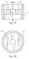
- FIG. 1is a cross section of a microwave downstream plasma asher.
- FIG. 2is a cross section of an orifice installed in a passageway between a plasma-generating region and a processing chamber.
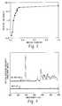
- FIG. 3is a graphical illustration depicting relative ion density at the wafer surface as a function of orifice diameter for an O 2 /(H 2 /N 2 )/CF 4 plasma.
- FIG. 4is a graphical illustration of the optical emission intensity for different pressure conditions as a function of wavelength.
- FIG. 5is a graph depicting a fourier transform infrared analysis (FTIR) of absorbance as a function of wavelength for different operating conditions.
- FTIRFourier transform infrared analysis
- the plasma ashing processcan be practiced on semiconductor substrates including, but not limited to, substrates having low k dielectric surfaces without damaging the low k material.
- increasing the pressure within a plasma-generating regionreduces the plasma ion density delivered to the substrate surface.
- a narrow orifice or orificesare preferably installed in an opening between the plasma-generating region and a substrate-processing chamber.
- the plasma-generating region pressurecreates a pressure differential greater than about 2 torr between the region and the processing chamber.
- Plasma asher devices particularly suitable for practicing the present inventionare downstream plasma ashers, such as for example, those microwave plasma ashers available under the trade name Fusion GEMINI ES® and commercially available from Axcelis Technologies, Inc. in Rockville, Md. Portions of the microwave plasma asher are described in U.S. Pat. Nos. 5,571,439, 5,498,308, 6,082,374, 5,980,638, 5,961,851, 6,057,645, 6,225,745 and 4,341,592, and PCT International Application No.
- WO/97/37055all of which are incorporated herein by reference in their entireties.
- Other examples of plasma generating and discharge devicesthat may be utilized according to the present invention include ashers employing radio frequency (RF) energy to generate the plasma.
- RFradio frequency
- a single or multi-component gas mixtureflows into a plasma-generating region, wherein the gas is exposed to an energy source to generate a plasma.
- the plasmais then discharged from the plasma-generating region through an opening or openings into the processing chamber.
- the pressure within the processing chamberis preferably reduced to optimize residence time for highest reaction rate on the substrate.
- a pressure differentialexists between the plasma-generating region and processing chamber as a function of the gas flow into the plasma-generating region, e.g., plasma tube, the opening between the region and chamber, and the chamber.
- the pressure differentialis about 1 torr, wherein the pressure within the plasma-generating region is greater than the pressure within the process chamber. This relationship can be described mathematically as shown in equation (1).
- Ptrepresents the pressure within the plasma tube
- Fis the gas flow
- Cis the conductance of the opening between the plasma tube and the process chamber
- Pcis the pressure within the process chamber
- the present inventionis directed to increasing the pressure within the plasma-generating region to reduce the ion density content of the plasma generated.
- the pressure within the plasma -generating regionpreferably ranges from about 2 torr to about atmospheric pressure.
- the atmospheric pressure limitmay vary depending on the gas composition and the ability to strike and sustain a plasma.
- the increased pressure within the plasma -generating regioncreates a pressure differential greater than 2 torr between the region and the substrate processing chamber.
- the illustrated plasma asher device 10generally includes a processing chamber 12 and a plasma generating system 14 connected to and in communication with the processing chamber 12 by passageway 16 .
- the processing chamber 12encloses a semiconductor substrate 18 , i.e., wafer, with photoresist and/or posts etch residues thereon to be ashed.
- the wafer 18is supported by a chuck or pins 20 and is preferably heated to accelerate the reaction of the photoresist and/or post etch residues with the plasma.
- One or more baffle platesmay be present above the wafer to promote even distribution of the plasma.
- the pressure within the process chamber 12is reduced.
- the pressure within the chamber 12is maintained between about 1 torr to about 7 torr. More preferably, the pressure is maintained from about 1 torr to about 3 torr.
- the plasma generating system 14provides plasma to an interior of the processing chamber 12 .
- a gas box(not shown) controls the flow of gases into the plasma generating system 14 .
- the gasesare exposed to an excitable energy source.
- microwave energycan be generated by magnetron 24 to ionize the gases and form plasma in a plasma tube 22 .
- the passageway 16 as shown in this exampleis hereinafter referred to as the “no orifice” configuration. Operation of the plasma asher normally results in an operating pressure within the plasma tube 22 of about 1 torr greater than the operating pressure within the processing chamber 12 .
- an orifice 30is installed in passageway 16 between the plasma-generating region 14 and the processing chamber 12 .
- the orifice 30is adapted to narrow the opening of passageway 16 , thereby increasing the pressure within the plasma tube 22 .
- the orifice 30is preferably fabricated from a thermally stable and non-reactive material.
- the orifice 30is fabricated from quartz or aluminum oxide. The orifice 30 decreases the conductance between the plasma tube and the processing chamber and as such, pressure within the tube 22 is increased in proportion to the gas flow rate into the plasma tube.
- the orifice 30is a variable orifice, wherein an operator may externally control the pressure within plasma tube 22 by adjusting the size of the variable orifice opening.
- the variable orificemay be comprised of an iris employing rigid shutter elements of the design utilized in cameras.
- the orifice, variable orifice or fixed diameter orificecan be adapted to any shape, size or configuration to increase the operating pressure within the plasma tube 22 .
- the orificeis configured in the passageway 16 to generate a pressure differential of at least 2 torr between the process chamber 12 and the plasma-generating region 14 , wherein the pressure within the plasma-generating region is greater than the pressure within the chamber.
- the pressure generated within the plasma tube 22preferably ranges from about 2 torr to about atmospheric pressure.
- the atmospheric pressure limitmay vary depending on the gas composition and the ability to strike and sustain a plasma. While not wanting to be bound by theory, it is believed that by increasing the pressure within the plasma-generating region 14 , e.g., the plasma tube 22 , the ion density is reduced as a function of the reduction in the gas mean free path. The reduction in gas mean free path is believed to increase the likelihood of an ion colliding with a gas molecule or a surface undergoing charge exchange, thereby reducing ion density.
- Photoresistsare generally organic photosensitive films used for transfer of images to an underlying substrate.
- the present inventionis generally applicable to ashing those photoresists and etch residues thereof used in g-line, i-line, DUV, 193 nm, and 157 nm applications or the like.
- Thisincludes, but is not limited to, novolaks, polyvinylphenols, acrylates, acetals, polyimides, ketals, cyclic olefins or the like.
- Other photoresist formulations suitable for use in the present inventionwill be apparent to those skilled in the art in view of this disclosure.
- the photoresistmay be positive acting or negative acting depending on the photoresist chemistries and developers chosen.
- Advanced semiconductor fabricationutilizes insulating layers that typically include the use of low k materials that have dielectric constants less than about 3.0.
- the process employing a reduced ion density plasmacan be utilized without deleteriously damaging or modifying the properties of the low k surface.
- Important low k film propertiesinclude thickness and uniformity, dielectric constant, refractive index, adhesion, chemical resistance, thermal stability, pore size and distribution, coefficient of thermal expansion, glass transition temperature, film stress and copper diffusion coefficient.
- Low k dielectricscan be generally classified as one of three types: organic, porous and doped oxides.
- Organic low k dielectric materialsinclude polyimides, benzocyclobutene, parylenes and fluorocarbons.
- SILK®spin-on aromatic hydrocarbons referred to by the trademark SILK® and commercially available from Dow Chemical.
- SILK®contains no fluorine or silicon and has a reported dielectric constant of 2.6 to 2.8.
- porous low k dielectric materialsinclude nanoglass and aerogels.
- doped oxide low k dielectric materialsinclude hydrogen-doped oxides, e.g., hydrogen silsesquioxanes (HSQ), fluorine-doped oxides, e.g., fluorinated silicate glass (FSG) and carbon-doped oxides such as those available under the trademark CORAL®.
- HSQhydrogen silsesquioxanes
- FSGfluorine-doped oxides
- CORAL®carbon-doped oxides
- a spin-on HSQis commercially available from Dow Corning under the trademark FOx®.
- FOx®is reported to have a dielectric constant of 2.6 to 3.0.
- Hybrid carbon containing dielectricsare commercially available under the trademark HOSP®.
- Other examplesinclude xerogels and methyl silsesquioxanes (MSQ).
- MSQmethyl silsesquioxanes
- FIG. 3graphically illustrates the relative ion plasma density at the wafer surface as a function of the diameter of the orifice 30 .
- Decreasing the orifice diameter to less than about 0.4 inchesincreased the backpressure within the plasma tube 22 to an amount effective to significantly reduce the plasma ion density at the wafer surface.
- plasmawas generated from a mixture of oxygen gas, forming gas and a trickle amount of CF 4 . It is expected that other gas chemistries will produce similar results in response to decreasing the orifice diameter. Accordingly, the process is applicable to oxygen free, oxygen containing, fluorine plasmas and the like, such as those gas chemistries disclosed in pending U.S. patent application Ser. Nos. 09/368,553 and 09/434,617, to Han et al., incorporated herein by reference in their entireties.
- FIG. 4there is shown a graphical representation of the optical emission intensity for reactive species as a function of wavelength generated in oxygen free plasma.
- the oxygen free plasmais generated from a gas mixture containing a fluorine compound and a forming gas.
- Forming gasis a gas mixture that consists essentially of hydrogen and nitrogen gases.
- the use of forming gas in the gas mixtureis known by those skilled in the art to generate characteristic CN emission signals.
- the optical emission intensitywas monitored from plasma generated in a plasma asher configured with an orifice 70 installed in passageway 16 and in a plasma asher configured without an orifice, i.e., a “no orifice” configuration.
- the plasma asher configured with an orifice 30resulted in a pressure differential between the plasma tube 22 and the process chamber 12 of about 6 torr, which produced weak emission signals at 695 nm, 71 nm and 790 nm.
- the spectrumshows a sharp emission line at 387 nm and several smaller emission signal peaks in the 500 to 800 nm wavelength range.
- the datashows a redistribution of ions and radicals generated within the reduced ion density plasma.
- FIG. 5graphically illustrates a Fourier Transform Infrared Analysis (FTIR) of a low k surface before and after exposure to oxygen free plasma.
- FTIRFourier Transform Infrared Analysis
Landscapes
- Engineering & Computer Science (AREA)
- Chemical & Material Sciences (AREA)
- Physics & Mathematics (AREA)
- General Chemical & Material Sciences (AREA)
- Analytical Chemistry (AREA)
- Chemical Kinetics & Catalysis (AREA)
- Plasma & Fusion (AREA)
- Condensed Matter Physics & Semiconductors (AREA)
- General Physics & Mathematics (AREA)
- Manufacturing & Machinery (AREA)
- Computer Hardware Design (AREA)
- Microelectronics & Electronic Packaging (AREA)
- Power Engineering (AREA)
- Drying Of Semiconductors (AREA)
- Exposure Of Semiconductors, Excluding Electron Or Ion Beam Exposure (AREA)
Abstract
Description
Claims (4)
Priority Applications (4)
| Application Number | Priority Date | Filing Date | Title |
|---|---|---|---|
| US09/911,682US6548416B2 (en) | 2001-07-24 | 2001-07-24 | Plasma ashing process |
| PCT/US2002/023344WO2003010799A2 (en) | 2001-07-24 | 2002-07-22 | Plasma ashing process |
| AU2002332421AAU2002332421A1 (en) | 2001-07-24 | 2002-07-22 | Plasma ashing process |
| TW091116337ATW557477B (en) | 2001-07-24 | 2002-07-23 | Plasma ashing process |
Applications Claiming Priority (1)
| Application Number | Priority Date | Filing Date | Title |
|---|---|---|---|
| US09/911,682US6548416B2 (en) | 2001-07-24 | 2001-07-24 | Plasma ashing process |
Publications (2)
| Publication Number | Publication Date |
|---|---|
| US20030022511A1 US20030022511A1 (en) | 2003-01-30 |
| US6548416B2true US6548416B2 (en) | 2003-04-15 |
Family
ID=25430687
Family Applications (1)
| Application Number | Title | Priority Date | Filing Date |
|---|---|---|---|
| US09/911,682Expired - LifetimeUS6548416B2 (en) | 2001-07-24 | 2001-07-24 | Plasma ashing process |
Country Status (4)
| Country | Link |
|---|---|
| US (1) | US6548416B2 (en) |
| AU (1) | AU2002332421A1 (en) |
| TW (1) | TW557477B (en) |
| WO (1) | WO2003010799A2 (en) |
Cited By (59)
| Publication number | Priority date | Publication date | Assignee | Title |
|---|---|---|---|---|
| US20030052086A1 (en)* | 2001-09-20 | 2003-03-20 | Michinobu Mizumura | Etching method of organic insulating film |
| US20040235299A1 (en)* | 2003-05-22 | 2004-11-25 | Axcelis Technologies, Inc. | Plasma ashing apparatus and endpoint detection process |
| US20040238123A1 (en)* | 2003-05-22 | 2004-12-02 | Axcelis Technologies, Inc. | Plasma apparatus, gas distribution assembly for a plasma apparatus and processes therewith |
| US20050279380A1 (en)* | 2004-06-17 | 2005-12-22 | Uvtech Systems, Inc. | Method for surface cleaning |
| US20060130147A1 (en)* | 2004-12-15 | 2006-06-15 | Matthew Von-Maszewski | Method and system for detecting and stopping illegitimate communication attempts on the internet |
| US20070272270A1 (en)* | 2004-12-27 | 2007-11-29 | Kun-Yuan Liao | Single-wafer cleaning procedure |
| US20070281496A1 (en)* | 2006-05-30 | 2007-12-06 | Applied Materials, Inc. | Chemical vapor deposition of high quality flow-like silicon dioxide using a silicon containing precursor and atomic oxygen |
| US20070281448A1 (en)* | 2006-05-30 | 2007-12-06 | Applied Materials, Inc. | Novel deposition-plasma cure cycle process to enhance film quality of silicon dioxide |
| US20070277734A1 (en)* | 2006-05-30 | 2007-12-06 | Applied Materials, Inc. | Process chamber for dielectric gapfill |
| US20070281495A1 (en)* | 2006-05-30 | 2007-12-06 | Applied Materials, Inc. | Formation of high quality dielectric films of silicon dioxide for sti: usage of different siloxane-based precursors for harp ii - remote plasma enhanced deposition processes |
| US20070298585A1 (en)* | 2006-06-22 | 2007-12-27 | Applied Materials, Inc. | Dielectric deposition and etch back processes for bottom up gapfill |
| US20080026597A1 (en)* | 2006-05-30 | 2008-01-31 | Applied Materials, Inc. | Method for depositing and curing low-k films for gapfill and conformal film applications |
| WO2007140425A3 (en)* | 2006-05-30 | 2008-02-14 | Applied Materials Inc | Process chamber for dielectric gapfill |
| US20090061647A1 (en)* | 2007-08-27 | 2009-03-05 | Applied Materials, Inc. | Curing methods for silicon dioxide thin films deposited from alkoxysilane precursor with harp ii process |
| US20090104789A1 (en)* | 2007-10-22 | 2009-04-23 | Applied Materials, Inc. | Method and system for improving dielectric film quality for void free gap fill |
| US20090104791A1 (en)* | 2007-10-22 | 2009-04-23 | Applied Materials, Inc. A Delaware Corporation | Methods for Forming a Silicon Oxide Layer Over a Substrate |
| US20090104755A1 (en)* | 2007-10-22 | 2009-04-23 | Applied Materials, Inc. | High quality silicon oxide films by remote plasma cvd from disilane precursors |
| US20090104790A1 (en)* | 2007-10-22 | 2009-04-23 | Applied Materials, Inc. | Methods for Forming a Dielectric Layer Within Trenches |
| US20090120464A1 (en)* | 2007-11-08 | 2009-05-14 | Applied Materials, Inc. | Multi-port pumping system for substrate processing chambers |
| US20090120584A1 (en)* | 2007-11-08 | 2009-05-14 | Applied Materials, Inc. | Counter-balanced substrate support |
| US20090120368A1 (en)* | 2007-11-08 | 2009-05-14 | Applied Materials, Inc. | Rotating temperature controlled substrate pedestal for film uniformity |
| US20090277587A1 (en)* | 2008-05-09 | 2009-11-12 | Applied Materials, Inc. | Flowable dielectric equipment and processes |
| US20090280650A1 (en)* | 2008-05-09 | 2009-11-12 | Applied Materials, Inc. | Flowable dielectric equipment and processes |
| US20100081293A1 (en)* | 2008-10-01 | 2010-04-01 | Applied Materials, Inc. | Methods for forming silicon nitride based film or silicon carbon based film |
| US20110034035A1 (en)* | 2009-08-06 | 2011-02-10 | Applied Materials, Inc. | Stress management for tensile films |
| US20110034039A1 (en)* | 2009-08-06 | 2011-02-10 | Applied Materials, Inc. | Formation of silicon oxide using non-carbon flowable cvd processes |
| US20110045676A1 (en)* | 2009-08-18 | 2011-02-24 | Applied Materials, Inc. | Remote plasma source seasoning |
| US20110111137A1 (en)* | 2009-11-12 | 2011-05-12 | Applied Materials, Inc. | Curing non-carbon flowable cvd films |
| CN101326629B (en)* | 2006-05-30 | 2011-05-25 | 应用材料股份有限公司 | Process chamber for filling dielectric gap |
| US20110129616A1 (en)* | 2009-12-02 | 2011-06-02 | Applied Materials, Inc. | Oxygen-doping for non-carbon radical-component cvd films |
| US20110136347A1 (en)* | 2009-10-21 | 2011-06-09 | Applied Materials, Inc. | Point-of-use silylamine generation |
| US20110165347A1 (en)* | 2010-01-05 | 2011-07-07 | Applied Materials, Inc. | Dielectric film formation using inert gas excitation |
| US7994019B1 (en) | 2010-04-01 | 2011-08-09 | Applied Materials, Inc. | Silicon-ozone CVD with reduced pattern loading using incubation period deposition |
| US20110217851A1 (en)* | 2010-03-05 | 2011-09-08 | Applied Materials, Inc. | Conformal layers by radical-component cvd |
| US8153348B2 (en) | 2008-02-20 | 2012-04-10 | Applied Materials, Inc. | Process sequence for formation of patterned hard mask film (RFP) without need for photoresist or dry etch |
| US8236708B2 (en) | 2010-03-09 | 2012-08-07 | Applied Materials, Inc. | Reduced pattern loading using bis(diethylamino)silane (C8H22N2Si) as silicon precursor |
| US8304351B2 (en) | 2010-01-07 | 2012-11-06 | Applied Materials, Inc. | In-situ ozone cure for radical-component CVD |
| US8318584B2 (en) | 2010-07-30 | 2012-11-27 | Applied Materials, Inc. | Oxide-rich liner layer for flowable CVD gapfill |
| US8445078B2 (en) | 2011-04-20 | 2013-05-21 | Applied Materials, Inc. | Low temperature silicon oxide conversion |
| US8450191B2 (en) | 2011-01-24 | 2013-05-28 | Applied Materials, Inc. | Polysilicon films by HDP-CVD |
| US8466073B2 (en) | 2011-06-03 | 2013-06-18 | Applied Materials, Inc. | Capping layer for reduced outgassing |
| US8476142B2 (en) | 2010-04-12 | 2013-07-02 | Applied Materials, Inc. | Preferential dielectric gapfill |
| US20130210202A1 (en)* | 2012-02-14 | 2013-08-15 | Samsung Display Co., Ltd. | Method of planarizing substrate and method of manufacturing thin film transistor using the same |
| US8524004B2 (en) | 2010-06-16 | 2013-09-03 | Applied Materials, Inc. | Loadlock batch ozone cure |
| US8551891B2 (en) | 2011-10-04 | 2013-10-08 | Applied Materials, Inc. | Remote plasma burn-in |
| US8617989B2 (en) | 2011-09-26 | 2013-12-31 | Applied Materials, Inc. | Liner property improvement |
| US8629067B2 (en) | 2009-12-30 | 2014-01-14 | Applied Materials, Inc. | Dielectric film growth with radicals produced using flexible nitrogen/hydrogen ratio |
| US8647992B2 (en) | 2010-01-06 | 2014-02-11 | Applied Materials, Inc. | Flowable dielectric using oxide liner |
| US8664127B2 (en) | 2010-10-15 | 2014-03-04 | Applied Materials, Inc. | Two silicon-containing precursors for gapfill enhancing dielectric liner |
| US8716154B2 (en) | 2011-03-04 | 2014-05-06 | Applied Materials, Inc. | Reduced pattern loading using silicon oxide multi-layers |
| US8889566B2 (en) | 2012-09-11 | 2014-11-18 | Applied Materials, Inc. | Low cost flowable dielectric films |
| US9018108B2 (en) | 2013-01-25 | 2015-04-28 | Applied Materials, Inc. | Low shrinkage dielectric films |
| US9129778B2 (en) | 2011-03-18 | 2015-09-08 | Lam Research Corporation | Fluid distribution members and/or assemblies |
| US9144147B2 (en) | 2011-01-18 | 2015-09-22 | Applied Materials, Inc. | Semiconductor processing system and methods using capacitively coupled plasma |
| US9285168B2 (en) | 2010-10-05 | 2016-03-15 | Applied Materials, Inc. | Module for ozone cure and post-cure moisture treatment |
| US9404178B2 (en) | 2011-07-15 | 2016-08-02 | Applied Materials, Inc. | Surface treatment and deposition for reduced outgassing |
| US9412581B2 (en) | 2014-07-16 | 2016-08-09 | Applied Materials, Inc. | Low-K dielectric gapfill by flowable deposition |
| US10283321B2 (en) | 2011-01-18 | 2019-05-07 | Applied Materials, Inc. | Semiconductor processing system and methods using capacitively coupled plasma |
| US12009228B2 (en) | 2015-02-03 | 2024-06-11 | Applied Materials, Inc. | Low temperature chuck for plasma processing systems |
Families Citing this family (5)
| Publication number | Priority date | Publication date | Assignee | Title |
|---|---|---|---|---|
| US6620741B1 (en)* | 2002-06-10 | 2003-09-16 | Intel Corporation | Method for controlling etch bias of carbon doped oxide films |
| US20060137711A1 (en)* | 2004-12-27 | 2006-06-29 | Kun-Yuan Liao | Single-wafer cleaning procedure |
| DE102005062813B4 (en)* | 2005-12-27 | 2009-11-26 | Vega Grieshaber Kg | Level measuring system with safety shutdown at high temperatures |
| JP2007225363A (en)* | 2006-02-22 | 2007-09-06 | Hitachi Ltd | Magnetic sample inspection equipment |
| CN108666222B (en)* | 2017-04-01 | 2021-06-25 | 中芯国际集成电路制造(上海)有限公司 | Semiconductor structure and method of making the same |
Citations (13)
| Publication number | Priority date | Publication date | Assignee | Title |
|---|---|---|---|---|
| US4341592A (en) | 1975-08-04 | 1982-07-27 | Texas Instruments Incorporated | Method for removing photoresist layer from substrate by ozone treatment |
| US5498308A (en) | 1994-02-25 | 1996-03-12 | Fusion Systems Corp. | Plasma asher with microwave trap |
| US5571439A (en) | 1995-04-27 | 1996-11-05 | Fusion Systems Corporation | Magnetron variable power supply with moding prevention |
| WO1997037055A1 (en) | 1996-04-02 | 1997-10-09 | Fusion Systems Corporation | Plasma device and method utilizing azimuthally and axially uniform electric field |
| US5811022A (en)* | 1994-11-15 | 1998-09-22 | Mattson Technology, Inc. | Inductive plasma reactor |
| US5980638A (en) | 1997-01-30 | 1999-11-09 | Fusion Systems Corporation | Double window exhaust arrangement for wafer plasma processor |
| US6057645A (en) | 1997-12-31 | 2000-05-02 | Eaton Corporation | Plasma discharge device with dynamic tuning by a movable microwave trap |
| US6080529A (en)* | 1997-12-12 | 2000-06-27 | Applied Materials, Inc. | Method of etching patterned layers useful as masking during subsequent etching or for damascene structures |
| US6082374A (en) | 1996-09-24 | 2000-07-04 | Huffman; Maria | Fluorine assisted stripping and residue removal in sapphire downstream plasma asher |
| US6211092B1 (en)* | 1998-07-09 | 2001-04-03 | Applied Materials, Inc. | Counterbore dielectric plasma etch process particularly useful for dual damascene |
| US6225745B1 (en) | 1999-12-17 | 2001-05-01 | Axcelis Technologies, Inc. | Dual plasma source for plasma process chamber |
| US6230651B1 (en)* | 1998-12-30 | 2001-05-15 | Lam Research Corporation | Gas injection system for plasma processing |
| US6331380B1 (en)* | 1997-12-12 | 2001-12-18 | Applied Materials, Inc. | Method of pattern etching a low K dielectric layer |
Family Cites Families (5)
| Publication number | Priority date | Publication date | Assignee | Title |
|---|---|---|---|---|
| WO1999026277A1 (en)* | 1997-11-17 | 1999-05-27 | Mattson Technology, Inc. | Systems and methods for plasma enhanced processing of semiconductor wafers |
| US6203657B1 (en)* | 1998-03-31 | 2001-03-20 | Lam Research Corporation | Inductively coupled plasma downstream strip module |
| JP2000026975A (en)* | 1998-07-09 | 2000-01-25 | Komatsu Ltd | Surface treatment equipment |
| US6492186B1 (en)* | 1999-08-05 | 2002-12-10 | Eaton Corporation | Method for detecting an endpoint for an oxygen free plasma process |
| DE10060002B4 (en)* | 1999-12-07 | 2016-01-28 | Komatsu Ltd. | Device for surface treatment |
- 2001
- 2001-07-24USUS09/911,682patent/US6548416B2/ennot_activeExpired - Lifetime
- 2002
- 2002-07-22AUAU2002332421Apatent/AU2002332421A1/ennot_activeAbandoned
- 2002-07-22WOPCT/US2002/023344patent/WO2003010799A2/ennot_activeApplication Discontinuation
- 2002-07-23TWTW091116337Apatent/TW557477B/enactive
Patent Citations (16)
| Publication number | Priority date | Publication date | Assignee | Title |
|---|---|---|---|---|
| US4341592A (en) | 1975-08-04 | 1982-07-27 | Texas Instruments Incorporated | Method for removing photoresist layer from substrate by ozone treatment |
| US5498308A (en) | 1994-02-25 | 1996-03-12 | Fusion Systems Corp. | Plasma asher with microwave trap |
| US5811022A (en)* | 1994-11-15 | 1998-09-22 | Mattson Technology, Inc. | Inductive plasma reactor |
| US5571439A (en) | 1995-04-27 | 1996-11-05 | Fusion Systems Corporation | Magnetron variable power supply with moding prevention |
| WO1997037055A1 (en) | 1996-04-02 | 1997-10-09 | Fusion Systems Corporation | Plasma device and method utilizing azimuthally and axially uniform electric field |
| US5961851A (en) | 1996-04-02 | 1999-10-05 | Fusion Systems Corporation | Microwave plasma discharge device |
| US6082374A (en) | 1996-09-24 | 2000-07-04 | Huffman; Maria | Fluorine assisted stripping and residue removal in sapphire downstream plasma asher |
| US5980638A (en) | 1997-01-30 | 1999-11-09 | Fusion Systems Corporation | Double window exhaust arrangement for wafer plasma processor |
| US6080529A (en)* | 1997-12-12 | 2000-06-27 | Applied Materials, Inc. | Method of etching patterned layers useful as masking during subsequent etching or for damascene structures |
| US6331380B1 (en)* | 1997-12-12 | 2001-12-18 | Applied Materials, Inc. | Method of pattern etching a low K dielectric layer |
| US6458516B1 (en)* | 1997-12-12 | 2002-10-01 | Applied Materials Inc. | Method of etching dielectric layers using a removable hardmask |
| US6057645A (en) | 1997-12-31 | 2000-05-02 | Eaton Corporation | Plasma discharge device with dynamic tuning by a movable microwave trap |
| US6211092B1 (en)* | 1998-07-09 | 2001-04-03 | Applied Materials, Inc. | Counterbore dielectric plasma etch process particularly useful for dual damascene |
| US6399511B2 (en)* | 1998-07-09 | 2002-06-04 | Applied Materials, Inc. | Plasma etch process in a single inter-level dielectric etch |
| US6230651B1 (en)* | 1998-12-30 | 2001-05-15 | Lam Research Corporation | Gas injection system for plasma processing |
| US6225745B1 (en) | 1999-12-17 | 2001-05-01 | Axcelis Technologies, Inc. | Dual plasma source for plasma process chamber |
Cited By (93)
| Publication number | Priority date | Publication date | Assignee | Title |
|---|---|---|---|---|
| US7014787B2 (en) | 2001-09-20 | 2006-03-21 | Hitachi, Ltd. | Etching method of organic insulating film |
| US6793833B2 (en)* | 2001-09-20 | 2004-09-21 | Hitachi, Ltd. | Etching method of organic insulating film |
| US20040182514A1 (en)* | 2001-09-20 | 2004-09-23 | Michinobu Mizumura | Etching method of organic insulating film |
| US20030052086A1 (en)* | 2001-09-20 | 2003-03-20 | Michinobu Mizumura | Etching method of organic insulating film |
| US7396481B2 (en) | 2001-09-20 | 2008-07-08 | Hitachi, Ltd. | Etching method of organic insulating film |
| KR100749839B1 (en)* | 2001-09-20 | 2007-08-16 | 가부시끼가이샤 히다치 세이사꾸쇼 | Etching method of organic insulating film |
| US20060065624A1 (en)* | 2001-09-20 | 2006-03-30 | Michinobu Mizumura | Etching method of organic insulating film |
| US20040238123A1 (en)* | 2003-05-22 | 2004-12-02 | Axcelis Technologies, Inc. | Plasma apparatus, gas distribution assembly for a plasma apparatus and processes therewith |
| US20040235299A1 (en)* | 2003-05-22 | 2004-11-25 | Axcelis Technologies, Inc. | Plasma ashing apparatus and endpoint detection process |
| US8268181B2 (en) | 2003-05-22 | 2012-09-18 | Axcelis Technologies, Inc. | Plasma ashing apparatus and endpoint detection process |
| US8580076B2 (en) | 2003-05-22 | 2013-11-12 | Lam Research Corporation | Plasma apparatus, gas distribution assembly for a plasma apparatus and processes therewith |
| US20100055807A1 (en)* | 2003-05-22 | 2010-03-04 | Axcelis Technologies, Inc. | Plasma ashing apparatus and endpoint detection process |
| US20050279453A1 (en)* | 2004-06-17 | 2005-12-22 | Uvtech Systems, Inc. | System and methods for surface cleaning |
| US20060231204A1 (en)* | 2004-06-17 | 2006-10-19 | Uvtech Systems, Inc. | Portable system for semiconductor manufacturing |
| US20050279380A1 (en)* | 2004-06-17 | 2005-12-22 | Uvtech Systems, Inc. | Method for surface cleaning |
| US7514015B2 (en) | 2004-06-17 | 2009-04-07 | Uvtech Systems | Method for surface cleaning |
| US20060130147A1 (en)* | 2004-12-15 | 2006-06-15 | Matthew Von-Maszewski | Method and system for detecting and stopping illegitimate communication attempts on the internet |
| US20070272270A1 (en)* | 2004-12-27 | 2007-11-29 | Kun-Yuan Liao | Single-wafer cleaning procedure |
| US7825038B2 (en) | 2006-05-30 | 2010-11-02 | Applied Materials, Inc. | Chemical vapor deposition of high quality flow-like silicon dioxide using a silicon containing precursor and atomic oxygen |
| US20070281496A1 (en)* | 2006-05-30 | 2007-12-06 | Applied Materials, Inc. | Chemical vapor deposition of high quality flow-like silicon dioxide using a silicon containing precursor and atomic oxygen |
| US20080026597A1 (en)* | 2006-05-30 | 2008-01-31 | Applied Materials, Inc. | Method for depositing and curing low-k films for gapfill and conformal film applications |
| US20090031953A1 (en)* | 2006-05-30 | 2009-02-05 | Applied Materials, Inc. | Chemical vapor deposition of high quality flow-like silicon dioxide using a silicon containing precursor and atomic oxygen |
| US7498273B2 (en) | 2006-05-30 | 2009-03-03 | Applied Materials, Inc. | Formation of high quality dielectric films of silicon dioxide for STI: usage of different siloxane-based precursors for harp II—remote plasma enhanced deposition processes |
| US7790634B2 (en) | 2006-05-30 | 2010-09-07 | Applied Materials, Inc | Method for depositing and curing low-k films for gapfill and conformal film applications |
| US20070277734A1 (en)* | 2006-05-30 | 2007-12-06 | Applied Materials, Inc. | Process chamber for dielectric gapfill |
| US20070281448A1 (en)* | 2006-05-30 | 2007-12-06 | Applied Materials, Inc. | Novel deposition-plasma cure cycle process to enhance film quality of silicon dioxide |
| CN101326629B (en)* | 2006-05-30 | 2011-05-25 | 应用材料股份有限公司 | Process chamber for filling dielectric gap |
| WO2007140425A3 (en)* | 2006-05-30 | 2008-02-14 | Applied Materials Inc | Process chamber for dielectric gapfill |
| US20070281495A1 (en)* | 2006-05-30 | 2007-12-06 | Applied Materials, Inc. | Formation of high quality dielectric films of silicon dioxide for sti: usage of different siloxane-based precursors for harp ii - remote plasma enhanced deposition processes |
| US7902080B2 (en) | 2006-05-30 | 2011-03-08 | Applied Materials, Inc. | Deposition-plasma cure cycle process to enhance film quality of silicon dioxide |
| US8232176B2 (en) | 2006-06-22 | 2012-07-31 | Applied Materials, Inc. | Dielectric deposition and etch back processes for bottom up gapfill |
| US20070298585A1 (en)* | 2006-06-22 | 2007-12-27 | Applied Materials, Inc. | Dielectric deposition and etch back processes for bottom up gapfill |
| US20090061647A1 (en)* | 2007-08-27 | 2009-03-05 | Applied Materials, Inc. | Curing methods for silicon dioxide thin films deposited from alkoxysilane precursor with harp ii process |
| US7745352B2 (en) | 2007-08-27 | 2010-06-29 | Applied Materials, Inc. | Curing methods for silicon dioxide thin films deposited from alkoxysilane precursor with harp II process |
| US20090104755A1 (en)* | 2007-10-22 | 2009-04-23 | Applied Materials, Inc. | High quality silicon oxide films by remote plasma cvd from disilane precursors |
| US8242031B2 (en) | 2007-10-22 | 2012-08-14 | Applied Materials, Inc. | High quality silicon oxide films by remote plasma CVD from disilane precursors |
| US20090104789A1 (en)* | 2007-10-22 | 2009-04-23 | Applied Materials, Inc. | Method and system for improving dielectric film quality for void free gap fill |
| US20090104791A1 (en)* | 2007-10-22 | 2009-04-23 | Applied Materials, Inc. A Delaware Corporation | Methods for Forming a Silicon Oxide Layer Over a Substrate |
| US7541297B2 (en) | 2007-10-22 | 2009-06-02 | Applied Materials, Inc. | Method and system for improving dielectric film quality for void free gap fill |
| US7803722B2 (en) | 2007-10-22 | 2010-09-28 | Applied Materials, Inc | Methods for forming a dielectric layer within trenches |
| US7943531B2 (en) | 2007-10-22 | 2011-05-17 | Applied Materials, Inc. | Methods for forming a silicon oxide layer over a substrate |
| US7867923B2 (en) | 2007-10-22 | 2011-01-11 | Applied Materials, Inc. | High quality silicon oxide films by remote plasma CVD from disilane precursors |
| US20090104790A1 (en)* | 2007-10-22 | 2009-04-23 | Applied Materials, Inc. | Methods for Forming a Dielectric Layer Within Trenches |
| US20090120584A1 (en)* | 2007-11-08 | 2009-05-14 | Applied Materials, Inc. | Counter-balanced substrate support |
| US20090120464A1 (en)* | 2007-11-08 | 2009-05-14 | Applied Materials, Inc. | Multi-port pumping system for substrate processing chambers |
| US20090120368A1 (en)* | 2007-11-08 | 2009-05-14 | Applied Materials, Inc. | Rotating temperature controlled substrate pedestal for film uniformity |
| US7964040B2 (en) | 2007-11-08 | 2011-06-21 | Applied Materials, Inc. | Multi-port pumping system for substrate processing chambers |
| US8153348B2 (en) | 2008-02-20 | 2012-04-10 | Applied Materials, Inc. | Process sequence for formation of patterned hard mask film (RFP) without need for photoresist or dry etch |
| US8357435B2 (en) | 2008-05-09 | 2013-01-22 | Applied Materials, Inc. | Flowable dielectric equipment and processes |
| US20090280650A1 (en)* | 2008-05-09 | 2009-11-12 | Applied Materials, Inc. | Flowable dielectric equipment and processes |
| US20090277587A1 (en)* | 2008-05-09 | 2009-11-12 | Applied Materials, Inc. | Flowable dielectric equipment and processes |
| US20100081293A1 (en)* | 2008-10-01 | 2010-04-01 | Applied Materials, Inc. | Methods for forming silicon nitride based film or silicon carbon based film |
| US7935643B2 (en) | 2009-08-06 | 2011-05-03 | Applied Materials, Inc. | Stress management for tensile films |
| US20110034035A1 (en)* | 2009-08-06 | 2011-02-10 | Applied Materials, Inc. | Stress management for tensile films |
| US8741788B2 (en) | 2009-08-06 | 2014-06-03 | Applied Materials, Inc. | Formation of silicon oxide using non-carbon flowable CVD processes |
| US20110034039A1 (en)* | 2009-08-06 | 2011-02-10 | Applied Materials, Inc. | Formation of silicon oxide using non-carbon flowable cvd processes |
| US20110045676A1 (en)* | 2009-08-18 | 2011-02-24 | Applied Materials, Inc. | Remote plasma source seasoning |
| US7989365B2 (en) | 2009-08-18 | 2011-08-02 | Applied Materials, Inc. | Remote plasma source seasoning |
| US20110136347A1 (en)* | 2009-10-21 | 2011-06-09 | Applied Materials, Inc. | Point-of-use silylamine generation |
| US8449942B2 (en) | 2009-11-12 | 2013-05-28 | Applied Materials, Inc. | Methods of curing non-carbon flowable CVD films |
| US20110111137A1 (en)* | 2009-11-12 | 2011-05-12 | Applied Materials, Inc. | Curing non-carbon flowable cvd films |
| US20110129616A1 (en)* | 2009-12-02 | 2011-06-02 | Applied Materials, Inc. | Oxygen-doping for non-carbon radical-component cvd films |
| US8980382B2 (en) | 2009-12-02 | 2015-03-17 | Applied Materials, Inc. | Oxygen-doping for non-carbon radical-component CVD films |
| US8629067B2 (en) | 2009-12-30 | 2014-01-14 | Applied Materials, Inc. | Dielectric film growth with radicals produced using flexible nitrogen/hydrogen ratio |
| US20110165347A1 (en)* | 2010-01-05 | 2011-07-07 | Applied Materials, Inc. | Dielectric film formation using inert gas excitation |
| US8329262B2 (en) | 2010-01-05 | 2012-12-11 | Applied Materials, Inc. | Dielectric film formation using inert gas excitation |
| US8647992B2 (en) | 2010-01-06 | 2014-02-11 | Applied Materials, Inc. | Flowable dielectric using oxide liner |
| US8304351B2 (en) | 2010-01-07 | 2012-11-06 | Applied Materials, Inc. | In-situ ozone cure for radical-component CVD |
| US8563445B2 (en) | 2010-03-05 | 2013-10-22 | Applied Materials, Inc. | Conformal layers by radical-component CVD |
| US20110217851A1 (en)* | 2010-03-05 | 2011-09-08 | Applied Materials, Inc. | Conformal layers by radical-component cvd |
| US8236708B2 (en) | 2010-03-09 | 2012-08-07 | Applied Materials, Inc. | Reduced pattern loading using bis(diethylamino)silane (C8H22N2Si) as silicon precursor |
| US7994019B1 (en) | 2010-04-01 | 2011-08-09 | Applied Materials, Inc. | Silicon-ozone CVD with reduced pattern loading using incubation period deposition |
| US8476142B2 (en) | 2010-04-12 | 2013-07-02 | Applied Materials, Inc. | Preferential dielectric gapfill |
| US8524004B2 (en) | 2010-06-16 | 2013-09-03 | Applied Materials, Inc. | Loadlock batch ozone cure |
| US8318584B2 (en) | 2010-07-30 | 2012-11-27 | Applied Materials, Inc. | Oxide-rich liner layer for flowable CVD gapfill |
| US9285168B2 (en) | 2010-10-05 | 2016-03-15 | Applied Materials, Inc. | Module for ozone cure and post-cure moisture treatment |
| US8664127B2 (en) | 2010-10-15 | 2014-03-04 | Applied Materials, Inc. | Two silicon-containing precursors for gapfill enhancing dielectric liner |
| US9144147B2 (en) | 2011-01-18 | 2015-09-22 | Applied Materials, Inc. | Semiconductor processing system and methods using capacitively coupled plasma |
| US10283321B2 (en) | 2011-01-18 | 2019-05-07 | Applied Materials, Inc. | Semiconductor processing system and methods using capacitively coupled plasma |
| US8450191B2 (en) | 2011-01-24 | 2013-05-28 | Applied Materials, Inc. | Polysilicon films by HDP-CVD |
| US8716154B2 (en) | 2011-03-04 | 2014-05-06 | Applied Materials, Inc. | Reduced pattern loading using silicon oxide multi-layers |
| US9129778B2 (en) | 2011-03-18 | 2015-09-08 | Lam Research Corporation | Fluid distribution members and/or assemblies |
| US8445078B2 (en) | 2011-04-20 | 2013-05-21 | Applied Materials, Inc. | Low temperature silicon oxide conversion |
| US8466073B2 (en) | 2011-06-03 | 2013-06-18 | Applied Materials, Inc. | Capping layer for reduced outgassing |
| US9404178B2 (en) | 2011-07-15 | 2016-08-02 | Applied Materials, Inc. | Surface treatment and deposition for reduced outgassing |
| US8617989B2 (en) | 2011-09-26 | 2013-12-31 | Applied Materials, Inc. | Liner property improvement |
| US8551891B2 (en) | 2011-10-04 | 2013-10-08 | Applied Materials, Inc. | Remote plasma burn-in |
| US9093535B2 (en)* | 2012-02-14 | 2015-07-28 | Samsung Display Co., Ltd. | Method of planarizing substrate and method of manufacturing thin film transistor using the same |
| US20130210202A1 (en)* | 2012-02-14 | 2013-08-15 | Samsung Display Co., Ltd. | Method of planarizing substrate and method of manufacturing thin film transistor using the same |
| US8889566B2 (en) | 2012-09-11 | 2014-11-18 | Applied Materials, Inc. | Low cost flowable dielectric films |
| US9018108B2 (en) | 2013-01-25 | 2015-04-28 | Applied Materials, Inc. | Low shrinkage dielectric films |
| US9412581B2 (en) | 2014-07-16 | 2016-08-09 | Applied Materials, Inc. | Low-K dielectric gapfill by flowable deposition |
| US12009228B2 (en) | 2015-02-03 | 2024-06-11 | Applied Materials, Inc. | Low temperature chuck for plasma processing systems |
Also Published As
| Publication number | Publication date |
|---|---|
| WO2003010799A3 (en) | 2003-10-02 |
| AU2002332421A1 (en) | 2003-02-17 |
| WO2003010799A2 (en) | 2003-02-06 |
| US20030022511A1 (en) | 2003-01-30 |
| TW557477B (en) | 2003-10-11 |
Similar Documents
| Publication | Publication Date | Title |
|---|---|---|
| US6548416B2 (en) | Plasma ashing process | |
| WO2002093634A1 (en) | Plasma ashing process | |
| US6207583B1 (en) | Photoresist ashing process for organic and inorganic polymer dielectric materials | |
| US7399712B1 (en) | Method for etching organic hardmasks | |
| US6834656B2 (en) | Plasma process for removing polymer and residues from substrates | |
| US6281135B1 (en) | Oxygen free plasma stripping process | |
| US8664124B2 (en) | Method for etching organic hardmasks | |
| US6951823B2 (en) | Plasma ashing process | |
| US8716143B1 (en) | Plasma based photoresist removal system for cleaning post ash residue | |
| US20020151156A1 (en) | Process for removal of photoresist after post ion implantation | |
| SG193093A1 (en) | Method for etching organic hardmasks | |
| JP2010219550A (en) | Method of plasma etching of organic antireflection film | |
| WO2008073379A1 (en) | Method and apparatus for ashing a substrate using carbon dioxide | |
| US20120024314A1 (en) | Plasma mediated ashing processes | |
| US11654461B2 (en) | Plasma ashing method using residue gas analyzer | |
| US20050106875A1 (en) | Plasma ashing method | |
| US6743712B2 (en) | Method of making a semiconductor device by forming a masking layer with a tapered etch profile | |
| JP4359847B2 (en) | Drying process for low-k dielectric films | |
| JPH05275326A (en) | Resist ashing method |
Legal Events
| Date | Code | Title | Description |
|---|---|---|---|
| AS | Assignment | Owner name:AXCELIS TECHNOLOGIES, INC., MASSACHUSETTS Free format text:ASSIGNMENT OF ASSIGNORS INTEREST;ASSIGNORS:HAN, QUINGYUAN;BERRY, IVAN;SAKTHIVEL, PALANI;AND OTHERS;REEL/FRAME:012018/0180 Effective date:20010707 | |
| STCF | Information on status: patent grant | Free format text:PATENTED CASE | |
| FPAY | Fee payment | Year of fee payment:4 | |
| AS | Assignment | Owner name:SILICON VALLEY BANK, CALIFORNIA Free format text:SECURITY AGREEMENT;ASSIGNOR:AXCELIS TECHNOLOGIES, INC.;REEL/FRAME:020986/0143 Effective date:20080423 Owner name:SILICON VALLEY BANK,CALIFORNIA Free format text:SECURITY AGREEMENT;ASSIGNOR:AXCELIS TECHNOLOGIES, INC.;REEL/FRAME:020986/0143 Effective date:20080423 | |
| FPAY | Fee payment | Year of fee payment:8 | |
| AS | Assignment | Owner name:LAM RESEARCH CORPORATION, CALIFORNIA Free format text:ASSIGNMENT OF ASSIGNORS INTEREST;ASSIGNOR:AXCELIS TECHNOLOGIES, INC.;REEL/FRAME:029529/0757 Effective date:20121203 | |
| AS | Assignment | Owner name:AXCELIS TECHNOLOGIES, INC., MASSACHUSETTS Free format text:TERMINATION OF SECURITY AGREEMENT;ASSIGNOR:SILICON VALLEY BANK;REEL/FRAME:030302/0719 Effective date:20130411 | |
| FPAY | Fee payment | Year of fee payment:12 |