US6547454B2 - Method to align optical components to a substrate and other optical components - Google Patents
Method to align optical components to a substrate and other optical componentsDownload PDFInfo
- Publication number
- US6547454B2 US6547454B2US09/920,917US92091701AUS6547454B2US 6547454 B2US6547454 B2US 6547454B2US 92091701 AUS92091701 AUS 92091701AUS 6547454 B2US6547454 B2US 6547454B2
- Authority
- US
- United States
- Prior art keywords
- array
- optical
- optical devices
- aligning
- substrate
- Prior art date
- Legal status (The legal status is an assumption and is not a legal conclusion. Google has not performed a legal analysis and makes no representation as to the accuracy of the status listed.)
- Expired - Lifetime
Links
Images


Classifications
- G—PHYSICS
- G02—OPTICS
- G02B—OPTICAL ELEMENTS, SYSTEMS OR APPARATUS
- G02B6/00—Light guides; Structural details of arrangements comprising light guides and other optical elements, e.g. couplings
- G02B6/24—Coupling light guides
- G02B6/42—Coupling light guides with opto-electronic elements
- G02B6/4201—Packages, e.g. shape, construction, internal or external details
- G02B6/4219—Mechanical fixtures for holding or positioning the elements relative to each other in the couplings; Alignment methods for the elements, e.g. measuring or observing methods especially used therefor
- G02B6/4228—Passive alignment, i.e. without a detection of the degree of coupling or the position of the elements
- G02B6/423—Passive alignment, i.e. without a detection of the degree of coupling or the position of the elements using guiding surfaces for the alignment
- G—PHYSICS
- G02—OPTICS
- G02B—OPTICAL ELEMENTS, SYSTEMS OR APPARATUS
- G02B6/00—Light guides; Structural details of arrangements comprising light guides and other optical elements, e.g. couplings
- G02B6/24—Coupling light guides
- G02B6/42—Coupling light guides with opto-electronic elements
- G02B6/4201—Packages, e.g. shape, construction, internal or external details
- G02B6/4249—Packages, e.g. shape, construction, internal or external details comprising arrays of active devices and fibres
- G—PHYSICS
- G02—OPTICS
- G02B—OPTICAL ELEMENTS, SYSTEMS OR APPARATUS
- G02B6/00—Light guides; Structural details of arrangements comprising light guides and other optical elements, e.g. couplings
- G02B6/24—Coupling light guides
- G02B6/42—Coupling light guides with opto-electronic elements
- G02B6/4201—Packages, e.g. shape, construction, internal or external details
- G02B6/4204—Packages, e.g. shape, construction, internal or external details the coupling comprising intermediate optical elements, e.g. lenses, holograms
- G—PHYSICS
- G02—OPTICS
- G02B—OPTICAL ELEMENTS, SYSTEMS OR APPARATUS
- G02B6/00—Light guides; Structural details of arrangements comprising light guides and other optical elements, e.g. couplings
- G02B6/24—Coupling light guides
- G02B6/42—Coupling light guides with opto-electronic elements
- G02B6/4201—Packages, e.g. shape, construction, internal or external details
- G02B6/4219—Mechanical fixtures for holding or positioning the elements relative to each other in the couplings; Alignment methods for the elements, e.g. measuring or observing methods especially used therefor
- G02B6/422—Active alignment, i.e. moving the elements in response to the detected degree of coupling or position of the elements
- G02B6/4221—Active alignment, i.e. moving the elements in response to the detected degree of coupling or position of the elements involving a visual detection of the position of the elements, e.g. by using a microscope or a camera
- G02B6/4224—Active alignment, i.e. moving the elements in response to the detected degree of coupling or position of the elements involving a visual detection of the position of the elements, e.g. by using a microscope or a camera using visual alignment markings, e.g. index methods
- G—PHYSICS
- G02—OPTICS
- G02B—OPTICAL ELEMENTS, SYSTEMS OR APPARATUS
- G02B6/00—Light guides; Structural details of arrangements comprising light guides and other optical elements, e.g. couplings
- G02B6/24—Coupling light guides
- G02B6/42—Coupling light guides with opto-electronic elements
- G02B6/4292—Coupling light guides with opto-electronic elements the light guide being disconnectable from the opto-electronic element, e.g. mutually self aligning arrangements
Definitions
- Active alignmentuses the features of optical components to align optical fibers to an optoelectronic device.
- a devicesuch as a photodetector is used in alignment.
- the photodetectoris positioned at one end of the optical fiber, detecting the light from the surface emitting laser at the other end of the optical fiber.
- the optical fiber's position, relative to the surface emitting laseris adjusted until light hitting the photodetector reaches a maximum.
- the photodetectorsenses a maximum amount of light, the fiber is bonded in a permanent position.
- Increased manufacturing demandshave caused a need for replacement of this type of alignment, as it can be time consuming and costly.
- Electronic packaging assemblersoften use pick-and-place methodology to position electronic components for subsequent assembly. Components are picked from a component holder and placed on a substrate no more than 25 microns from an absolute reference position. This alignment tolerance is 5 times greater than that required for low-loss optical interconnects.
- a method and apparatusare provided for aligning an array of optical devices with optical processing equipment.
- the methodincludes the steps of providing a transparent substrate with a plurality of optical transmission paths passing directly through the substrate, providing a plurality of alignment guides on the optical array, providing a complementary plurality of respective alignment guides on the transparent substrate and guiding the optical devices of the array into alignment with the substrate using respective pairs of the alignment guides on the optical array and transparent substrate.
- FIG. 1is a perspective view of a waveguide system and a transparent substrate with corresponding guide pins under an illustrated embodiment of the invention
- FIG. 2is a top view of an optical array of FIG. 1 showing optical ports, electrical features and registration targets;
- FIG. 3is a top view of the optical array of FIG. 1 showing a plurality of alignment structures, as well as optical ports, electrical features and registration targets;
- FIG. 4is a cross-sectional view of an optical array and substrate of FIG. 1 with a plurality of alignment features placed on a substrate also containing a plurality of alignment features;
- FIG. 5is a cross-sectional view of an optical array, substrate and optical fiber of FIG. 1 under an alternate embodiment
- FIG. 6is a side cut-away view of an alignment feature of the optical array of FIG. 4;
- FIG. 7is a top view of an optical via that may be used with the system of FIG. 1;
- FIG. 8is a transparent substrate of FIG. 1 containing a layer of a dielectric material
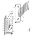
- FIG. 9is an perspective view of a optical system of FIG. 1 under an alternate embodiment wherein the array and substrate are disposed within a sealed can, further connected to a plurality of optical fibers;
- FIG. 10is a top view of an array of optical systems of FIG. 1 disposed on a single, common transparent substrate.
- FIG. 1shows an optical coupler and converter assembly 31 in a context of use and generally in accordance with an illustrated embodiment of the invention.
- the optically transparent substrate 5may be attached to a guide pin holder 27 .
- Both the substrate 5 and guide pin holder 27may be attached to a common printed circuit board (PCB) 28 .
- Transmission paths 25 of the optical array 8(FIG. 2) pass through the optically transparent substrate 5 .
- An external waveguide coupler 26 containing optical fibers 12may be aligned to the optically clear substrate 5 and the optical array 8 .
- the optically transparent substrate 5may be provided with guide pin apertures 21 .
- Guide pin apertures 21may be laser drilled to relatively close tolerances for insertion of the guide pins 22 .
- the external waveguide coupler 26may contains guide pin apertures 24 for receiving guide pins 22 and for aligning the optical fibers 12 to the transparent substrate 5 .
- the guide pin apertures 24 and/or guide pins 22form alignment references for coupling the converter assembly 31 to other optical devices.
- FIG. 1shows guide pins held in place by an accompanying pin holder 27 .
- the pins 22are placed through the optically transparent substrate 5 , and the external waveguide system 26 is aligned to the optical array by operation of the substrate 5 which functions as an alignment substrate that aligns the transmission paths of the optical array 8 with the transmission paths of the fibers 12 .
- the optical assembly 31is shown in the context of converting between an electrical signal on the PCB 28 and an optical signal on the fibers 12 , it should be understood that the converter assembly 31 may be used in any of a number of other applications.
- the assembly 31could be coupled electrically to a communication cable and optically coupled to another optical array on a circuit board using the guide pins 22 for alignment to form an electro-optical isolator.
- FIG. 2shows an optical array 8 containing optical ports 1 (e.g., VCSEL lasers, DFB lasers, photodetectors, etc.) with transmission paths 25 extending normal to the top surface (i.e., out of the page). Thus, the direction of light is normal to the surface of interest.
- the optical array 8may be fabricated using conventional techniques.
- the assembly process of the optical array 8could use registration targets 4 to generally locate the position of the optical array 8 on the corresponding substrate 5 (as described in more detail below).
- the electrical traces 2 , electrical pads 3 , or optical ports 1could also be used as registration targets.
- the scope of the registration targetsis not limited to one or the other, but could include a combination of registration targets.
- electrical traces 2 and optical ports 1could both be used as registration targets 4 in determining the location of the optical array 8 on the array substrate 5 .
- other alignment structures and featurescan also be placed on the surface to further guide the array 8 into a precise alignment with the transparent substrate 5 .
- the distances from the registration targets to the outer boundaries of the optical device 8may be programmed into the pick and place machinery. Thus, the delivered location of the optical array 8 by the pick and place machinery is known.
- a series of alignment devices 6 , 7may be fabricated on mating surfaces of the array 8 and substrate 5 .
- the alignment devicesmay be fabricated on the same side of the array 8 as the ports 1 . In some cases (described below) the alignment devices may be fabricated directly over the ports 1 .
- the registration and alignment features 6 , 7 on the optical array 8are not limited to any type of material, or any particular location on the surface of the optical array.
- the registration featuresare not limited to any number either. For instance, there could be ‘m’ optical ports 1 , ‘n’ electrical pads 3 , and ‘o’ electrical traces 2 , and some combination used as registration features.
- FIG. 4shows a layer 29 of polyimid may be disposed over the mating surfaces of the array 8 and substrate 5 .
- the layer 29 of polyimidmay be any commercially available photoreactive material (e.g., 20-100 microns thick) provided with an associated etching agent.
- a maskmay be placed over the polyimid layer on the array 8 .
- the maskmay transmit (or block) light in areas defining the alignment devices 6 , 7 .
- the mask and layermay then be exposed and the excess material etched away to leave the devices 6 , 7 , shown in FIG. 3 .
- the devicesmay be round, square or any other shape.
- a maskmay be placed over the polyimid layer 29 disposed on the substrate 5 .
- the mask on the substrate 5may be aligned to the holes 21 .
- the polyimid layer 29may be exposed and excess material etched away.
- the alignment devices 6 , 7may be provided as complementary post and receptacle type devices (FIG. 4 ).
- Posts 6 , 7may be fabricated on the array 8 and complementary receptacles 9 may be fabricated on the substrate 5 .
- any combination of posts 6 , 7 and receptacles 9may be placed on the array 8 or substrate, the only limitation being that any corresponding locations on the array 8 and substrate 5 would include a complementary pair of alignment devices 6 , 7 and 9 .
- the registration featuresi.e., alignment devices
- the alignment devices 7are optically transparent, they can be placed over the active optical regions of the ports 1 , as shown in FIG. 3 .
- the alignment devices 7When placed over the optically active regions, the alignment devices 7 have been found to function as a lens, directing light along a predictable path through the substrate 5 into the fibers 12 .
- these alignment structures 6 , 7may have tapered sides of different sizes and profiles that may be used to guide and align the optical-component to the mating substrate 5 .
- Alignment features 6are not limited to the optical array 8 though.
- complementary alignment features 6 , 7 , 9can be placed on the substrate 5 or on the metal traces 11 .
- the metal traces 11may be disposed on the substrate 5 and used to connect the pads 3 to external connections (e.g., on a supporting printed circuit board).
- a combination of alignment features 6 , 7 , 9 on both the substrate and optical array surfacecan be used in guiding and aligning the components to their proper location.
- FIG. 4illustrates the relationship between the alignment features 6 , 7 of the optical array 8 and those corresponding features 9 of the substrate 5 .
- the structure of the alignment features 6 , 7 , 9functions to guide the optical component 8 into its correct position on the substrate 5 .
- the substrate 5could have built-up sections or removed areas 9 , such as guide pin apertures 21 , (see FIG. 1 ), depending on the desired features for the application.
- the substrate 5could also have on its surface a layer of a polyimid 29 or similar material. This material might be easier in manufacturing to a desired shape or form.
- FIG. 5illustrates what a substrate 5 might look like with a polyimid layer 29 between the optical array 8 and the substrate 5 and with conductive traces partially disposed over the layer 29 .
- Alignment features 6 , 7 on the substrate 5 or polyimidare not limited to one side. They could be located on the surface closest to the optical fiber 12 or on the surface closest to the optical array 8 .
- the initial physical placement of the optical components 8can be done using standard pick-and-place equipment.
- Optical alignmentoccurs as the alignment features 6 , 7 , 9 engage and lock into a final position. Tapered edges 18 , 19 of the alignment features allow a smooth initial placement, and automatic movement into the optical alignment.
- the tapered alignment features ( 18 , 19 ) of both surfacescan be of different sizes in order to complete the alignment process.
- the tolerances 16 of the pick and place machinemay be comparable in scope to the operable range of the alignment feature 6 , as shown in FIG. 6 . Otherwise, the initial alignment of the features may not be close enough to render the tapered sides functional. Thus, the range of self-alignment provided by the alignment features 6 would be expected to be larger than the pick and place machinery tolerance 16 .
- the tapered surfaces 18 , 19may be shaped using any of a number of different methods. Under a first method, the natural process of etching may be used to control the rate of taper. Since an etchant would be expected to etch at a constant rate, it would be expected that a top of a hole 9 may have a larger diameter than a bottom of the hole.
- the mask used to create the receptaclemay have feathered edges, thereby increasing an etching rate around a periphery of an entry location of the hole.
- varying degrees of tapermay be achieved.
- the same process used for the receptacles 9may be applied to the posts 6 , 7 .
- a feathering of the maskmay be used to achieve any desired amount of taper.
- the diameter of the tip of the post 6 , 7may be approximately 70 microns.
- the diameter at the bottom of the receptaclemay also be 70 microns.
- the taper of the post 6 , 7may be 45 degrees.
- the taper of the receptaclemay be 45-70 degrees.
- the array 8may be placed at least 70 microns to either side of the center of the receptacle 9 and still operatively engage the receptacle 9 . Alignment would be achieved in this example because gravity would cause the tapered post 6 , 7 to slide down the tapered receptacle 9 until the post 6 , 7 reaches the bottom of the receptacle 9 . When the post reaches the bottom of the receptacle 9 , substantially complete alignment would be achieved.
- taper of the post 6 , 7functions to further shape and direct optical transmission.
- the tapered post 6 , 7may form a frustrum-shaped lens directing light along an optical transmission path passing through the substrate 5 .
- optical arrays 8may be held in place by a mass rapid bonding process. Bonding could include adhesives, solder, stud bumps, or a similar material.
- the alignment materialis transparent such as a polyimid
- the materialcan be modified to form an optical-wavefront transforming structure, as shown in FIG. 5 .
- the alignment deviceis a lens and lens receptacle 9 .
- Such structuresmay include, but are not limited to negative or positive lens, Fresnel lens, or optical guide, allowing more efficient coupling of the light between the active optical component 1 and a light guiding device such as an optical fiber 12 .
- An optical-wavefront transforming or confining structurehere called an optical via (or waveguide) 15 , can also be made in the optical transparent substrate 5 .
- FIG. 7light is guided through the area encompassed by the holes 17 , normal to the surface of the page.
- the figureillustrates how a system of confining light might look.
- the apertures 17 in the substrate 5may be filled with a polyimid, or similar substance having an index of refraction lower than that of the substrate's 5 . With a lower index of refraction in the apertures 17 , light will be reflected away from the apertures 17 .
- the apertures 17would then act as a light confining structure by deflecting light towards the center of the circular structure.
- These apertures 17are not limited to a certain type of filling, but could be left unfilled (i.e., filled with air).
- the index of refraction of the substrate 5could be changed to direct light as desired.
- Material diffusion, compression, or ultraviolet exposureare examples of methods of creating an index step in refraction to change a boundary region from guiding to non-guiding regions.
- Antireflection coatings and structurescan also be used and structured in the package to minimize the coupling losses between the active optical components 8 and passive optical waveguide coupler 26 . They may be disposed on the surface of the substrate 5 nearest to the optical fiber 12 .
- solder bumps 10may be used to electrically connect the package traces 2 to the optical components. These traces can go to other electro-optic components (not shown).
- Alignment of optical fibers 12can be determined by alignment apertures 21 through the substrates or by structures built upon the substrate, as shown in FIG. 6 . These features, in turn, may be defined using photolithographic registration targets 4 on the substrate 5 and provide the alignment that is required between the active optical-component ports 1 and the optical fiber 12 .
- the assembly shown in FIG. 8can be placed in a housing 23 and sealed, as shown in FIG. 9 .
- Guide pins 22 mounted in the housing 23 or guide structures fabricated on the transparent substrate 5will guide the waveguide connector assembly 26 to the active optical ports 1 .
- FIG. 10illustrates how optical components may be placed on a large transparent substrate 30 .
- the substrate 30may then be placed on a test bed that has electrical connections (bed of electrical probes or pads) to electrically activate these devices.
- the optical characteristics of these devicescan be accessed through the transparent substrate 30 , which is on the opposite side of the structure from the electrical interconnects.
- large arrays of optical assemblies 31can be simultaneously burned-in and tested before connection to other devices.
- the common substrate 30is partitioned (cut into assemblies 31 ) and the further packaging can be completed.
Landscapes
- Physics & Mathematics (AREA)
- General Physics & Mathematics (AREA)
- Optics & Photonics (AREA)
- Optical Couplings Of Light Guides (AREA)
Abstract
Description
Claims (33)
Priority Applications (7)
| Application Number | Priority Date | Filing Date | Title |
|---|---|---|---|
| US09/920,917US6547454B2 (en) | 2000-09-21 | 2001-08-02 | Method to align optical components to a substrate and other optical components |
| CA002422986ACA2422986A1 (en) | 2000-09-21 | 2001-08-20 | Method to align optical components to a substrate and other optical components |
| PCT/US2001/025818WO2002025341A1 (en) | 2000-09-21 | 2001-08-20 | Method to align optical components to a substrate and other optical components |
| JP2002529283AJP2004525391A (en) | 2000-09-21 | 2001-08-20 | Method for aligning an optical component with a substrate and other optical components |
| EP01968017AEP1328837A1 (en) | 2000-09-21 | 2001-08-20 | Method to align optical components to a substrate and other optical components |
| AU2001288296AAU2001288296A1 (en) | 2000-09-21 | 2001-08-20 | Method to align optical components to a substrate and other optical components |
| US10/368,707US6793409B2 (en) | 2000-09-21 | 2003-02-19 | Method to align optical components to a substrate and other optical components |
Applications Claiming Priority (2)
| Application Number | Priority Date | Filing Date | Title |
|---|---|---|---|
| US23412600P | 2000-09-21 | 2000-09-21 | |
| US09/920,917US6547454B2 (en) | 2000-09-21 | 2001-08-02 | Method to align optical components to a substrate and other optical components |
Related Child Applications (1)
| Application Number | Title | Priority Date | Filing Date |
|---|---|---|---|
| US10/368,707DivisionUS6793409B2 (en) | 2000-09-21 | 2003-02-19 | Method to align optical components to a substrate and other optical components |
Publications (2)
| Publication Number | Publication Date |
|---|---|
| US20020034363A1 US20020034363A1 (en) | 2002-03-21 |
| US6547454B2true US6547454B2 (en) | 2003-04-15 |
Family
ID=26927593
Family Applications (2)
| Application Number | Title | Priority Date | Filing Date |
|---|---|---|---|
| US09/920,917Expired - LifetimeUS6547454B2 (en) | 2000-09-21 | 2001-08-02 | Method to align optical components to a substrate and other optical components |
| US10/368,707Expired - Fee RelatedUS6793409B2 (en) | 2000-09-21 | 2003-02-19 | Method to align optical components to a substrate and other optical components |
Family Applications After (1)
| Application Number | Title | Priority Date | Filing Date |
|---|---|---|---|
| US10/368,707Expired - Fee RelatedUS6793409B2 (en) | 2000-09-21 | 2003-02-19 | Method to align optical components to a substrate and other optical components |
Country Status (6)
| Country | Link |
|---|---|
| US (2) | US6547454B2 (en) |
| EP (1) | EP1328837A1 (en) |
| JP (1) | JP2004525391A (en) |
| AU (1) | AU2001288296A1 (en) |
| CA (1) | CA2422986A1 (en) |
| WO (1) | WO2002025341A1 (en) |
Cited By (7)
| Publication number | Priority date | Publication date | Assignee | Title |
|---|---|---|---|---|
| US20030031431A1 (en)* | 2001-08-07 | 2003-02-13 | Ronald Kunkel | Assembly for aligning an optical array with optical fibers |
| US6600853B2 (en)* | 2000-09-21 | 2003-07-29 | Corona Optical Systems, Inc. | Electro-optic interconnect circuit board |
| US6724961B2 (en)* | 2002-02-14 | 2004-04-20 | Corona Optical Systems, Inc. | Method to assemble optical components to a substrate |
| US20040212802A1 (en)* | 2001-02-20 | 2004-10-28 | Case Steven K. | Optical device with alignment compensation |
| US20050135726A1 (en)* | 2003-12-19 | 2005-06-23 | Industrial Technology Research Institute | Array optical subassembly for array optical active component |
| US20080239295A1 (en)* | 2007-03-28 | 2008-10-02 | Verizon Services Organization Inc. | Optical power monitoring with robotically moved macro-bending |
| US20170181604A1 (en)* | 2014-03-17 | 2017-06-29 | Intuitive Surgical Operations, Inc. | Multi-stage instrument connector |
Families Citing this family (15)
| Publication number | Priority date | Publication date | Assignee | Title |
|---|---|---|---|---|
| US7086134B2 (en)* | 2000-08-07 | 2006-08-08 | Shipley Company, L.L.C. | Alignment apparatus and method for aligning stacked devices |
| US6759687B1 (en)* | 2000-10-13 | 2004-07-06 | Agilent Technologies, Inc. | Aligning an optical device system with an optical lens system |
| US6450701B1 (en)* | 2001-05-14 | 2002-09-17 | Schott Optovance, Inc. | Transforming optical fiber interconnect array |
| US6633700B2 (en)* | 2001-07-31 | 2003-10-14 | Corning Incorporated | Double lens array for optical cross-connects |
| US7165895B2 (en)* | 2002-09-16 | 2007-01-23 | Emcore Corporation | Method of guiding an optical signal |
| TWI242938B (en)* | 2004-02-20 | 2005-11-01 | Ind Tech Res Inst | Parallel optical subassembly module structure |
| JP4238187B2 (en) | 2004-07-21 | 2009-03-11 | ヒロセ電機株式会社 | Photoelectric composite connector and board using the same |
| US7308167B2 (en)* | 2004-09-01 | 2007-12-11 | Agilent Technologies, Inc. | Optical assembly with optoelectronic device alignment |
| US7861031B2 (en)* | 2007-03-01 | 2010-12-28 | Hewlett-Packard Development Company, L.P. | Access control management |
| TW201441699A (en)* | 2013-04-23 | 2014-11-01 | Hon Hai Prec Ind Co Ltd | Optical communication module |
| WO2017039681A1 (en) | 2015-09-04 | 2017-03-09 | Ccs Technology, Inc. | Fiber coupling device for coupling of at last one optical fiber |
| CN109900390B (en)* | 2019-04-02 | 2021-02-23 | 珠海格力电器股份有限公司 | Rapid and accurate thermal bulb fault detection method and air conditioning unit |
| US11035752B1 (en)* | 2020-02-10 | 2021-06-15 | Psiquantum, Corp. | Active alignment of optical die to optical substrates |
| CN113514982A (en)* | 2021-04-12 | 2021-10-19 | 惠州市华星光电技术有限公司 | Quantum dot lens and backlight module |
| US20230375336A1 (en)* | 2022-05-19 | 2023-11-23 | Quantinuum Llc | High precision photonic alignment device |
Citations (21)
| Publication number | Priority date | Publication date | Assignee | Title |
|---|---|---|---|---|
| US4730198A (en) | 1984-11-26 | 1988-03-08 | American Telephone And Telegraph Company, At&T Bell Laboratories | Aligning arrays of optoelectronic devices to arrays of optical fibers |
| US4779946A (en) | 1986-02-14 | 1988-10-25 | American Telephone And Telegraph Company, At&T Bell Laboratories | Microminiature optical assembly |
| US5091991A (en) | 1991-02-25 | 1992-02-25 | Amp Incorporated | Optical fiber connector with alignment feature |
| US5281301A (en) | 1991-05-24 | 1994-01-25 | At&T Laboratories | Alignment and assembly method |
| US5357593A (en) | 1993-10-12 | 1994-10-18 | Alliedsignal Inc. | Method of attaching optical fibers to opto-electronic integrated circuits on silicon substrates |
| US5432878A (en) | 1994-03-03 | 1995-07-11 | Cts Corporation | Silicon carrier for testing and alignment of optoelectronic devices and method of assembling same |
| US5539848A (en) | 1995-05-31 | 1996-07-23 | Motorola | Optical waveguide module and method of making |
| US5574814A (en) | 1995-01-31 | 1996-11-12 | Microelectronics And Computer Technology Corporation | Parallel optical transceiver link |
| US5590232A (en) | 1995-02-16 | 1996-12-31 | Motorola, Inc. | Optical package and method of making |
| US5703973A (en) | 1996-03-29 | 1997-12-30 | Lucent Technologies Inc. | Optical integrated circuit having passively aligned fibers and method using same |
| US5768456A (en) | 1996-11-22 | 1998-06-16 | Motorola, Inc. | Optoelectronic package including photonic device mounted in flexible substrate |
| US5815616A (en) | 1997-01-02 | 1998-09-29 | Lucent Technologies Inc. | Optical packaging assembly for reflective devices |
| US5857049A (en) | 1997-05-05 | 1999-01-05 | Lucent Technologies, Inc., | Precision alignment of optoelectronic devices |
| US5898806A (en) | 1991-11-07 | 1999-04-27 | Nec Corporation | Optical interconnection circuit structure |
| US5909524A (en) | 1996-05-20 | 1999-06-01 | Fujitsu Limited | Optical coupling structure and a fabrication process thereof |
| US5940558A (en) | 1997-01-02 | 1999-08-17 | Lucent Technologies, Inc. | Optical packaging assembly for transmissive devices |
| JPH11307869A (en)* | 1998-04-22 | 1999-11-05 | Furukawa Electric Co Ltd:The | Array optical element module |
| US6034808A (en) | 1998-02-04 | 2000-03-07 | Mitel Semiconductor Ab | Multiple function optical module having electromagnetic shielding |
| US6095697A (en) | 1998-03-31 | 2000-08-01 | Honeywell International Inc. | Chip-to-interface alignment |
| US6112002A (en) | 1996-11-29 | 2000-08-29 | Fujitsu Limited | Optical coupler optically coupling a light beam of a semiconductor laser source with a single mode optical waveguide or fiber |
| US6118917A (en) | 1997-07-31 | 2000-09-12 | Samsung Electronics Co., Ltd. | Optical fiber passive alignment apparatus using alignment platform |
Family Cites Families (5)
| Publication number | Priority date | Publication date | Assignee | Title |
|---|---|---|---|---|
| US4741595A (en)* | 1984-07-13 | 1988-05-03 | Hitachi, Ltd. | Optical transmission device |
| US5802236A (en)* | 1997-02-14 | 1998-09-01 | Lucent Technologies Inc. | Article comprising a micro-structured optical fiber, and method of making such fiber |
| JPH10111750A (en) | 1996-10-03 | 1998-04-28 | Toyota Motor Corp | Wiring model generation device and generation method |
| JP3715425B2 (en)* | 1998-03-06 | 2005-11-09 | ブラザー工業株式会社 | Manufacturing method of substrate with optical waveguide |
| US6097870A (en)* | 1999-05-17 | 2000-08-01 | Lucent Technologies Inc. | Article utilizing optical waveguides with anomalous dispersion at vis-nir wavelenghts |
- 2001
- 2001-08-02USUS09/920,917patent/US6547454B2/ennot_activeExpired - Lifetime
- 2001-08-20CACA002422986Apatent/CA2422986A1/ennot_activeAbandoned
- 2001-08-20AUAU2001288296Apatent/AU2001288296A1/ennot_activeAbandoned
- 2001-08-20JPJP2002529283Apatent/JP2004525391A/enactivePending
- 2001-08-20WOPCT/US2001/025818patent/WO2002025341A1/ennot_activeApplication Discontinuation
- 2001-08-20EPEP01968017Apatent/EP1328837A1/ennot_activeWithdrawn
- 2003
- 2003-02-19USUS10/368,707patent/US6793409B2/ennot_activeExpired - Fee Related
Patent Citations (21)
| Publication number | Priority date | Publication date | Assignee | Title |
|---|---|---|---|---|
| US4730198A (en) | 1984-11-26 | 1988-03-08 | American Telephone And Telegraph Company, At&T Bell Laboratories | Aligning arrays of optoelectronic devices to arrays of optical fibers |
| US4779946A (en) | 1986-02-14 | 1988-10-25 | American Telephone And Telegraph Company, At&T Bell Laboratories | Microminiature optical assembly |
| US5091991A (en) | 1991-02-25 | 1992-02-25 | Amp Incorporated | Optical fiber connector with alignment feature |
| US5281301A (en) | 1991-05-24 | 1994-01-25 | At&T Laboratories | Alignment and assembly method |
| US5898806A (en) | 1991-11-07 | 1999-04-27 | Nec Corporation | Optical interconnection circuit structure |
| US5357593A (en) | 1993-10-12 | 1994-10-18 | Alliedsignal Inc. | Method of attaching optical fibers to opto-electronic integrated circuits on silicon substrates |
| US5432878A (en) | 1994-03-03 | 1995-07-11 | Cts Corporation | Silicon carrier for testing and alignment of optoelectronic devices and method of assembling same |
| US5574814A (en) | 1995-01-31 | 1996-11-12 | Microelectronics And Computer Technology Corporation | Parallel optical transceiver link |
| US5590232A (en) | 1995-02-16 | 1996-12-31 | Motorola, Inc. | Optical package and method of making |
| US5539848A (en) | 1995-05-31 | 1996-07-23 | Motorola | Optical waveguide module and method of making |
| US5703973A (en) | 1996-03-29 | 1997-12-30 | Lucent Technologies Inc. | Optical integrated circuit having passively aligned fibers and method using same |
| US5909524A (en) | 1996-05-20 | 1999-06-01 | Fujitsu Limited | Optical coupling structure and a fabrication process thereof |
| US5768456A (en) | 1996-11-22 | 1998-06-16 | Motorola, Inc. | Optoelectronic package including photonic device mounted in flexible substrate |
| US6112002A (en) | 1996-11-29 | 2000-08-29 | Fujitsu Limited | Optical coupler optically coupling a light beam of a semiconductor laser source with a single mode optical waveguide or fiber |
| US5815616A (en) | 1997-01-02 | 1998-09-29 | Lucent Technologies Inc. | Optical packaging assembly for reflective devices |
| US5940558A (en) | 1997-01-02 | 1999-08-17 | Lucent Technologies, Inc. | Optical packaging assembly for transmissive devices |
| US5857049A (en) | 1997-05-05 | 1999-01-05 | Lucent Technologies, Inc., | Precision alignment of optoelectronic devices |
| US6118917A (en) | 1997-07-31 | 2000-09-12 | Samsung Electronics Co., Ltd. | Optical fiber passive alignment apparatus using alignment platform |
| US6034808A (en) | 1998-02-04 | 2000-03-07 | Mitel Semiconductor Ab | Multiple function optical module having electromagnetic shielding |
| US6095697A (en) | 1998-03-31 | 2000-08-01 | Honeywell International Inc. | Chip-to-interface alignment |
| JPH11307869A (en)* | 1998-04-22 | 1999-11-05 | Furukawa Electric Co Ltd:The | Array optical element module |
Cited By (15)
| Publication number | Priority date | Publication date | Assignee | Title |
|---|---|---|---|---|
| US6600853B2 (en)* | 2000-09-21 | 2003-07-29 | Corona Optical Systems, Inc. | Electro-optic interconnect circuit board |
| US7369334B2 (en) | 2001-02-20 | 2008-05-06 | Cyberoptics Corporation | Optical device with alignment compensation |
| US20040212802A1 (en)* | 2001-02-20 | 2004-10-28 | Case Steven K. | Optical device with alignment compensation |
| US20030031431A1 (en)* | 2001-08-07 | 2003-02-13 | Ronald Kunkel | Assembly for aligning an optical array with optical fibers |
| US6860650B2 (en)* | 2001-08-07 | 2005-03-01 | Corona Optical Systems, Inc. | Assembly for aligning an optical array with optical fibers |
| US6724961B2 (en)* | 2002-02-14 | 2004-04-20 | Corona Optical Systems, Inc. | Method to assemble optical components to a substrate |
| US7440646B2 (en) | 2003-12-19 | 2008-10-21 | Industrial Technology Research Institute | Array optical subassembly for array optical active component |
| US20050135726A1 (en)* | 2003-12-19 | 2005-06-23 | Industrial Technology Research Institute | Array optical subassembly for array optical active component |
| US20080239295A1 (en)* | 2007-03-28 | 2008-10-02 | Verizon Services Organization Inc. | Optical power monitoring with robotically moved macro-bending |
| US7574082B2 (en)* | 2007-03-28 | 2009-08-11 | Verizon Services Organization Inc. | Optical power monitoring with robotically moved macro-bending |
| US20090244524A1 (en)* | 2007-03-28 | 2009-10-01 | Verizon Services Organization Inc. | Optical power monitoring with robotically moved macro-bending |
| US8014640B2 (en)* | 2007-03-28 | 2011-09-06 | Verizon Patent And Licensing Inc. | Optical power monitoring with robotically moved macro-bending |
| US20170181604A1 (en)* | 2014-03-17 | 2017-06-29 | Intuitive Surgical Operations, Inc. | Multi-stage instrument connector |
| US10631713B2 (en)* | 2014-03-17 | 2020-04-28 | Intuitive Surgical Operations, Inc. | Multi-stage instrument connector |
| US11382493B2 (en)* | 2014-03-17 | 2022-07-12 | Intuitive Surgical Operations, Inc. | Multi-stage instrument connector |
Also Published As
| Publication number | Publication date |
|---|---|
| US20020034363A1 (en) | 2002-03-21 |
| JP2004525391A (en) | 2004-08-19 |
| WO2002025341A1 (en) | 2002-03-28 |
| EP1328837A1 (en) | 2003-07-23 |
| CA2422986A1 (en) | 2002-03-28 |
| AU2001288296A1 (en) | 2002-04-02 |
| US6793409B2 (en) | 2004-09-21 |
| US20030147600A1 (en) | 2003-08-07 |
Similar Documents
| Publication | Publication Date | Title |
|---|---|---|
| US6547454B2 (en) | Method to align optical components to a substrate and other optical components | |
| US10684419B2 (en) | Waveguide connector elements and optical assemblies incorporating the same | |
| US20230418004A1 (en) | Multi-fiber interface apparatus for photonic integrated circuit | |
| US11852870B2 (en) | Optical fiber photonic integrated chip connector interfaces, photonic integrated chip assemblies, and methods of fabricating the same | |
| US6241399B1 (en) | Ferrule assembly and optical module | |
| EP0982610B1 (en) | Optical subassembly for use in fiber optic data transmission and reception | |
| US6599029B2 (en) | Ferrule assembly and receptacle type optical transmission module | |
| US20250237822A1 (en) | Detachable Connector for Co-Packaged Optics | |
| US9170387B2 (en) | Optical component assemblies | |
| US20060251360A1 (en) | Flip-chip mountable optical connector for chip-to-chip optical interconnectability | |
| EP1410085A2 (en) | Module mounted aligning optical connector | |
| EP3345029A1 (en) | Fiber coupling device for coupling of at last one optical fiber | |
| Karppinen et al. | Parallel optical interconnect between ceramic BGA packages on FR4 board using embedded waveguides and passive optical alignments | |
| US6868207B2 (en) | Method to diffract and attenuate an optical signal | |
| JP2015079061A (en) | Optical module, electronic instrument using the same, and assembly method of optical module | |
| US7165895B2 (en) | Method of guiding an optical signal | |
| US6764227B2 (en) | Interconnecting optical components with passive alignment | |
| KR20010076771A (en) | Silicon optical bench and plastic molded receptacle for reception it and optical subassembly constructed them | |
| Karppinen et al. | Parallel optical interconnect between surface-mounted devices on FR4 printed wiring board using embedded waveguides and passive optical alignments | |
| Jones et al. | Hybrid integration using silicon optical motherboards |
Legal Events
| Date | Code | Title | Description |
|---|---|---|---|
| AS | Assignment | Owner name:CORONA OPTICAL SYSTEMS, INC., ILLINOIS Free format text:ASSIGNMENT OF ASSIGNORS INTEREST;ASSIGNORS:WICKMAN, RANDY;GREENE, JOHN;O'CONNOR, GARY;AND OTHERS;REEL/FRAME:012061/0192;SIGNING DATES FROM 20010718 TO 20010727 | |
| STCF | Information on status: patent grant | Free format text:PATENTED CASE | |
| FEPP | Fee payment procedure | Free format text:PAT HOLDER NO LONGER CLAIMS SMALL ENTITY STATUS, ENTITY STATUS SET TO UNDISCOUNTED (ORIGINAL EVENT CODE: STOL); ENTITY STATUS OF PATENT OWNER: LARGE ENTITY | |
| FPAY | Fee payment | Year of fee payment:4 | |
| AS | Assignment | Owner name:EMCORE CORPORATION, NEW JERSEY Free format text:ASSIGNMENT OF ASSIGNORS INTEREST;ASSIGNOR:CORONA OPTICAL SYSTEMS, INC.;REEL/FRAME:019287/0396 Effective date:20040629 | |
| AS | Assignment | Owner name:BANK OF AMERICA, N.A., ILLINOIS Free format text:SECURITY AGREEMENT;ASSIGNOR:EMCORE CORPORATION;REEL/FRAME:021824/0019 Effective date:20080926 Owner name:BANK OF AMERICA, N.A.,ILLINOIS Free format text:SECURITY AGREEMENT;ASSIGNOR:EMCORE CORPORATION;REEL/FRAME:021824/0019 Effective date:20080926 | |
| FPAY | Fee payment | Year of fee payment:8 | |
| AS | Assignment | Owner name:WELLS FARGO BANK, NATIONAL ASSOCIATION, ARIZONA Free format text:SECURITY AGREEMENT;ASSIGNORS:EMCORE CORPORATION;EMCORE SOLAR POWER, INC.;REEL/FRAME:026304/0142 Effective date:20101111 | |
| AS | Assignment | Owner name:EMCORE CORPORATION, NEW MEXICO Free format text:RELEASE BY SECURED PARTY;ASSIGNOR:BANK OF AMERICA, N.A.;REEL/FRAME:027050/0880 Effective date:20110831 Owner name:EMCORE SOLAR POWER, INC., NEW MEXICO Free format text:RELEASE BY SECURED PARTY;ASSIGNOR:BANK OF AMERICA, N.A.;REEL/FRAME:027050/0880 Effective date:20110831 | |
| AS | Assignment | Owner name:EMCORE SOLAR POWER, INC., NEW MEXICO Free format text:PARTIAL RELEASE OF SECURITY INTEREST;ASSIGNOR:WELLS FARGO BANK, NATIONAL ASSOCIATION;REEL/FRAME:028192/0189 Effective date:20120507 Owner name:EMCORE CORPORATION, NEW MEXICO Free format text:PARTIAL RELEASE OF SECURITY INTEREST;ASSIGNOR:WELLS FARGO BANK, NATIONAL ASSOCIATION;REEL/FRAME:028192/0189 Effective date:20120507 | |
| FEPP | Fee payment procedure | Free format text:PAYOR NUMBER ASSIGNED (ORIGINAL EVENT CODE: ASPN); ENTITY STATUS OF PATENT OWNER: LARGE ENTITY | |
| AS | Assignment | Owner name:SUMITOMO ELECTRIC DEVICE INNOVATIONS, U.S.A., INC. Free format text:ASSIGNMENT OF ASSIGNORS INTEREST;ASSIGNOR:EMCORE CORPORATION;REEL/FRAME:030006/0126 Effective date:20130225 | |
| FPAY | Fee payment | Year of fee payment:12 |