US6546517B1 - Semiconductor memory - Google Patents
Semiconductor memoryDownload PDFInfo
- Publication number
- US6546517B1 US6546517B1US09/488,676US48867600AUS6546517B1US 6546517 B1US6546517 B1US 6546517B1US 48867600 AUS48867600 AUS 48867600AUS 6546517 B1US6546517 B1US 6546517B1
- Authority
- US
- United States
- Prior art keywords
- ram
- program codes
- semiconductor memory
- storage region
- program
- Prior art date
- Legal status (The legal status is an assumption and is not a legal conclusion. Google has not performed a legal analysis and makes no representation as to the accuracy of the status listed.)
- Expired - Lifetime
Links
Images


Classifications
- G—PHYSICS
- G11—INFORMATION STORAGE
- G11C—STATIC STORES
- G11C16/00—Erasable programmable read-only memories
- G11C16/02—Erasable programmable read-only memories electrically programmable
- G11C16/06—Auxiliary circuits, e.g. for writing into memory
- G11C16/10—Programming or data input circuits
- G11C16/102—External programming circuits, e.g. EPROM programmers; In-circuit programming or reprogramming; EPROM emulators
- G11C16/105—Circuits or methods for updating contents of nonvolatile memory, especially with 'security' features to ensure reliable replacement, i.e. preventing that old data is lost before new data is reliably written
- G—PHYSICS
- G06—COMPUTING OR CALCULATING; COUNTING
- G06F—ELECTRIC DIGITAL DATA PROCESSING
- G06F11/00—Error detection; Error correction; Monitoring
- G06F11/07—Responding to the occurrence of a fault, e.g. fault tolerance
- G06F11/08—Error detection or correction by redundancy in data representation, e.g. by using checking codes
- G06F11/10—Adding special bits or symbols to the coded information, e.g. parity check, casting out 9's or 11's
- G—PHYSICS
- G06—COMPUTING OR CALCULATING; COUNTING
- G06F—ELECTRIC DIGITAL DATA PROCESSING
- G06F8/00—Arrangements for software engineering
- G06F8/60—Software deployment
- G06F8/61—Installation
- G—PHYSICS
- G11—INFORMATION STORAGE
- G11C—STATIC STORES
- G11C16/00—Erasable programmable read-only memories
- G11C16/02—Erasable programmable read-only memories electrically programmable
- G11C16/06—Auxiliary circuits, e.g. for writing into memory
- G11C16/10—Programming or data input circuits
- G11C16/102—External programming circuits, e.g. EPROM programmers; In-circuit programming or reprogramming; EPROM emulators
Definitions
- the present inventionrelates to a semiconductor memory and, more particularly, to a semiconductor disk device and a flash ATA (AT attachment) card which employ, for example, flash memories.
- a semiconductor disk deviceand a flash ATA (AT attachment) card which employ, for example, flash memories.
- flash ATAAT attachment
- a semiconductor disk device, a flash ATA card and the likehave been proposed as external memories for computers, and comprise bulk flash memories for storing data therein and a controller for controlling the bulk flash memories.
- the controllerincludes a CPU (central processing unit) and a firmware memory for storing programs known as firmware.
- firmwarecentral processing unit
- the use of a ROM (read-only memory) as the firmware memoryis disadvantageous in that firmware is not readily modified since every modification and every version update of the firmware require the ROM to be remade.
- a technique which uses a RAM (random access memory) as the firmware memoryhas hence been proposed such that firmware previously stored in part of flash memories is loaded to the RAM at power-on and a program loaded to the RAM is executed.
- FIG. 4conceptually illustrates a relationship between a RAM map and a flash memory map when the above described technique is employed.
- the firmware stored in the flash memories as illustrated in the flash memory mapis loaded to the RAM as illustrated in the RAM map when power is turned on.
- Such a methodis advantageous in that modification and version update of the firmware are readily carried out by rewriting the firmware to be stored in the flash memories.
- a semiconductor memorycomprises: a nonvolatile semiconductor storage section having a plurality of rewritable, individually accessible blocks for individually storing therein a plurality of program codes each corresponding to one process, respectively; a RAM including a first storage region for mutually exclusively storing the plurality of program codes therein; and an error correcting section connected between the RAM and the nonvolatile semiconductor storage section and for transferring one of the plurality of program codes to the RAM while performing error correction upon the one of the plurality of program codes.
- the RAMfurther includes a second storage region for storing therein a starting address of each of the plurality of blocks.
- each of the plurality of program codesis associated with a command provided from an outside of the semiconductor memory.
- the semiconductor memory according to the first aspect of the present inventionis designed such that the modification of firmware or the addition of a function of the firmware require only the modification of the nonvolatile semiconductor storage section, eliminating the need to remake the ROM. Additionally, the semiconductor memory of the first aspect is high in expandability since the increase in the size of a program provided by the modification of the firmware or the addition of a function of the firmware does not require the increase in the capacity of the first storage region of the RAM, and is low in costs because of the provision of a greater number of functions with a smaller RAM capacity. Furthermore, the error correction is performed on the program being transferred from the nonvolatile semiconductor storage section to the RAM, to preclude a program in which an uncorrectable error occurs from being loaded to the RAM.
- the starting addresses of the respective blocksare stored in the second storage region before the program codes are loaded. This eliminates the need to access the nonvolatile semiconductor storage section each time one of the program codes is stored in the first storage region, achieving rapid operation.
- the semiconductor memory according to the third aspect of the present inventioncan easily add a function without remaking the ROM and increasing the size of the RAM capacity if there is a need to support a new command because of a review of specifications or the addition of an option.
- FIG. 1is a block diagram of a semiconductor memory according to a preferred embodiment of the present invention.
- FIG. 2conceptually illustrates a relationship between a RAM map and a flash memory map according to the preferred embodiment of the present invention
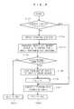
- FIG. 3is a flowchart showing the operation of the preferred embodiment of the present invention.
- FIG. 4conceptually illustrates a background art relationship between the RAM map and the flash memory map.
- FIG. 1is a block diagram of a flash ATA card 100 illustrated as a semiconductor memory according to a preferred embodiment of the present invention.
- the flash ATA card 100is connected to an external device through an ATA bus 51 , and comprises a host interface 7 connected to the ATA bus 51 .
- a commandis inputted from an external host computer through the ATA bus 51 and the host interface 7 to a host bus 52 , and data is outputted from the ATA bus 51 to the external host computer.
- the flash ATA card 100further comprises a buffer RAM 5 connected to the host interface 7 through the host bus 52 , a flash memory group 4 connected to the buffer RAM 5 through a flash bus 53 , and a controller 8 connected to the buffer RAM 5 through a CPU bus 54 .
- the flash memory group 4is constructed to be accessible on a block-by-block (sector-by-sector) basis to meet a bulk data storage application.
- the flash memory group 4comprises a plurality of flash memories 41 , 42 , . . . , 4 m.
- the flash memory group 4may consist of a single flash memory if it is accessible on a block-by-block basis.
- the controller 8comprises a CPU 1 , a RAM 2 and a ROM 3 which are connected to each other through the CPU bus 54 .
- FIG. 2conceptually illustrates a relationship between a RAM map and a flash memory map in the flash ATA card 100 .
- Firmware stored in the flash memories as illustrated in the flash memory maphas a plurality of program codes corresponding respectively to first to N-th processing routines, e.g., differing from each other, and each of the program codes is stored in a single block.
- locations in which the program codes are storedare represented in FIG. 2 by their corresponding processing routines, respectively.
- the RAM 2includes a first storage region 91 serving as a dynamic load area to which a program code stored in each of the blocks of the flash memory group 4 is exclusively loaded. Such program code transfer from the flash memory group 4 to the RAM 2 is executed, e.g., by the CPU 1 based on a program previously stored in the ROM 3 .
- the present inventionis adapted to mutually exclusively load the plurality of program codes each corresponding to the respective one processing routine to the first storage region 91 , requiring a smaller size of the RAM 2 than the size of the background art RAM shown in FIG. 4 .
- the firmwaremay be, of course, subjected to modification and version update. In this case, the required size of the RAM 2 is not increased. If a program code corresponding to a new additional processing routine is greater than the program code stored in each of the blocks of the flash memory group 4 , the additional processing routine may be divided into parts which in turn are stored in blocks, respectively, of the flash memory group 4 , whereby there is no need to change the size of the RAM 2 .
- the RAM 2may further include a second storage region 92 , in which case starting addresses of the blocks which store the program codes corresponding to the first to N-th processing routines, respectively, are also stored in the form of a table in the flash memory group 4 .
- This tableis loaded to the second storage region 92 of the RAM 2 .
- Such table loadingis required to be carried out only once, for example, at power-on, to save the time for reading a starting address from the flash memory group 4 each time a program code is loaded, thereby achieving rapid operation.
- Such table transfer from the flash memory group 4 to the RAM 2is also executed, e.g., by the CPU 1 based on a program previously stored in the ROM 3 .
- an ECC (error checking and correcting) circuit 6is connected to the flash bus 53 to store a program code called from the flash memory group 4 once in the buffer RAM 5 while performing the error correction on the program code. If there is no uncorrectable error in the program code, the program code is transferred from the buffer RAM 5 to the RAM 2 . This precludes the program code in which an uncorrectable error occurs from being loaded to the RAM 2 . Such an operation is also executed, e.g., by the CPU 1 based on a program previously stored in the ROM 3 .
- the capacity of the buffer RAM 5is required to be as small as one program code having the largest size. Further, the buffer RAM 5 is accessible from the CPU 1 and the external host computer, and the CPU 1 and the external host computer can analyze the program code in which an uncorrectable error occurs.
- the ROM 3 and the RAM 2may, of course, store therein program codes and data other than those described above.
- FIG. 3is a flowchart showing the operation of the flash ATA card 100 loading firmware to the RAM 2 .
- Step S 101whether or not the program code corresponding to the k-th processing routine is stored in the first storage region 91 serving as the dynamic load area is checked. More specifically, whether or not there is a match between the number of the processing routine corresponding to the already loaded program code and the number k of the processing routine to be executed is checked.
- Step S 107the CPU 1 executes the program code stored in the first storage region 91 . More specifically, the CPU 1 causes an address jump to the first storage region 91 to execute the program code. Then, the flow proceeds to Step S 202 to return to a main routine for transition to other processing. At this time, information indicating, in the main routine to which the return is made, that the program code is normally stored is also transmitted (as indicated by “OK” in Step S 202 of FIG. 3 ).
- Step S 101If it is judged in Step S 101 that the program code corresponding to the k-th processing routine is not stored in the first storage region 91 , it is necessary to store a new program code in the first storage region 91 . Then, in Step S 102 , the table stored in the second storage region 92 is referred to, and the starting address of the block in which the program code corresponding to the k-th processing routine is stored is obtained from the table.
- Step S 103the program code corresponding to the k-th processing routine is obtained from the block starting at the obtained starting address, and is transferred to the buffer RAM 5 while being subjected to ECC processing (error correction).
- ECC processingerror correction
- Step S 105the program code stored in the buffer RAM 5 is copied to the first storage region 91 .
- Step S 107the CPU 1 executes the program code stored in the first storage region 91 . Then, the flow proceeds to Step S 202 to return to the main routine for transition to other processing.
- Steps S 201 and S 202The return is made in Steps S 201 and S 202 to an address pointer which has called a routine having the flowchart of FIG. 3 .
- the processing routines corresponding to the program codes individually stored in the flash memory group 4may be associated with, for example, ATA command numbers, respectively.
- the processing routines corresponding to the program codes stored in the flash memory group 4are to be individually executed in accordance with the ATA commands from the host computer. This facilitates the addition of a function without remaking the ROM and increasing the size of the RAM capacity if there arises a need for support of a new ATA command because of the necessity of a future review of specifications or the addition of an option.
- the present inventionis suitably applied when the controller 8 is a single chip controller, in which case remaking the ROM and increasing the size of the RAM capacity require an extensive process involving a mask change and are not readily carried out.
- the present inventionnot only contribute to the ATA card but also may be similarly applied to other information processing devices comprising a RAM and flash memories, producing similar effects.
- a semiconductor disk devicemay be used as a flash memory so as to store bulk data.
Landscapes
- Engineering & Computer Science (AREA)
- Theoretical Computer Science (AREA)
- General Engineering & Computer Science (AREA)
- Physics & Mathematics (AREA)
- General Physics & Mathematics (AREA)
- Software Systems (AREA)
- Quality & Reliability (AREA)
- Computer Security & Cryptography (AREA)
- Techniques For Improving Reliability Of Storages (AREA)
- Stored Programmes (AREA)
Abstract
Description
Claims (15)
Applications Claiming Priority (2)
| Application Number | Priority Date | Filing Date | Title |
|---|---|---|---|
| JP11201617AJP2001027953A (en) | 1999-07-15 | 1999-07-15 | Semiconductor storage device |
| JP11-201617 | 1999-07-15 |
Publications (1)
| Publication Number | Publication Date |
|---|---|
| US6546517B1true US6546517B1 (en) | 2003-04-08 |
Family
ID=16444037
Family Applications (1)
| Application Number | Title | Priority Date | Filing Date |
|---|---|---|---|
| US09/488,676Expired - LifetimeUS6546517B1 (en) | 1999-07-15 | 2000-01-21 | Semiconductor memory |
Country Status (2)
| Country | Link |
|---|---|
| US (1) | US6546517B1 (en) |
| JP (1) | JP2001027953A (en) |
Cited By (17)
| Publication number | Priority date | Publication date | Assignee | Title |
|---|---|---|---|---|
| US20010052068A1 (en)* | 2000-01-13 | 2001-12-13 | Kei Kubota | Method of transferring program to internal memory from external memory and microcomputer using the same |
| US20020032891A1 (en)* | 2000-09-12 | 2002-03-14 | Hitachi, Ltd. | Data processing system and data processing method |
| US20030056065A1 (en)* | 2001-09-15 | 2003-03-20 | Thilo Jahn | Method and device for memory monitoring, in particular for RAM monitoring |
| US20030172295A1 (en)* | 2002-03-01 | 2003-09-11 | Onspec Electronics, Inc. | Device and system for allowing secure identification of an individual when accessing information and a method of use |
| US20050172207A1 (en)* | 2004-01-30 | 2005-08-04 | Radke William H. | Error detection and correction scheme for a memory device |
| US20060091658A1 (en)* | 2004-10-12 | 2006-05-04 | Robert Bosch Gmbh | Apparatus and method of compensating a seat offset for a load applied to the seat |
| US20060120191A1 (en)* | 2004-12-06 | 2006-06-08 | Mediatek Incorporation | Systems and methods for optical drive operation |
| US20070162626A1 (en)* | 2005-11-02 | 2007-07-12 | Iyer Sree M | System and method for enhancing external storage |
| US20080046637A1 (en)* | 2004-01-28 | 2008-02-21 | Yoshito Katano | Semiconductor Device and Processing Method for Starting the Same |
| US20080114994A1 (en)* | 2006-11-14 | 2008-05-15 | Sree Mambakkam Iyer | Method and system to provide security implementation for storage devices |
| US20080181406A1 (en)* | 2007-01-30 | 2008-07-31 | Technology Properties Limited | System and Method of Storage Device Data Encryption and Data Access Via a Hardware Key |
| US20080184035A1 (en)* | 2007-01-30 | 2008-07-31 | Technology Properties Limited | System and Method of Storage Device Data Encryption and Data Access |
| US20080288703A1 (en)* | 2007-05-18 | 2008-11-20 | Technology Properties Limited | Method and Apparatus of Providing Power to an External Attachment Device via a Computing Device |
| US20080288782A1 (en)* | 2007-05-18 | 2008-11-20 | Technology Properties Limited | Method and Apparatus of Providing Security to an External Attachment Device |
| US20090046858A1 (en)* | 2007-03-21 | 2009-02-19 | Technology Properties Limited | System and Method of Data Encryption and Data Access of a Set of Storage Devices via a Hardware Key |
| US20120198143A1 (en)* | 2009-10-08 | 2012-08-02 | International Business Machines Corporation | Memory Package Utilizing At Least Two Types of Memories |
| US20220382563A1 (en)* | 2021-05-31 | 2022-12-01 | Autochips Inc. | Program startup method, electronic system, and non-transitory storage medium |
Families Citing this family (5)
| Publication number | Priority date | Publication date | Assignee | Title |
|---|---|---|---|---|
| KR100482998B1 (en)* | 2002-08-30 | 2005-04-15 | 주식회사 하이닉스반도체 | Device for controlling of non-volatile ferroelectric memory |
| JP4308551B2 (en)* | 2003-03-06 | 2009-08-05 | 株式会社ルネサステクノロジ | Memory card and host device |
| GB2404748B (en)* | 2003-08-01 | 2006-10-04 | Symbian Ltd | Computing device and method |
| US7594135B2 (en)* | 2003-12-31 | 2009-09-22 | Sandisk Corporation | Flash memory system startup operation |
| JP2007334915A (en)* | 2007-08-27 | 2007-12-27 | Renesas Technology Corp | Memory card |
Citations (12)
| Publication number | Priority date | Publication date | Assignee | Title |
|---|---|---|---|---|
| US4484303A (en)* | 1979-06-19 | 1984-11-20 | Gould Inc. | Programmable controller |
| JPH01121933A (en) | 1987-11-06 | 1989-05-15 | Mitsubishi Electric Corp | microcontroller |
| US5511164A (en)* | 1995-03-01 | 1996-04-23 | Unisys Corporation | Method and apparatus for determining the source and nature of an error within a computer system |
| US5606660A (en)* | 1994-10-21 | 1997-02-25 | Lexar Microsystems, Inc. | Method and apparatus for combining controller firmware storage and controller logic in a mass storage system |
| US5659801A (en)* | 1994-12-07 | 1997-08-19 | Emc Corporation | Method and apparatus for replacing resident peripheral device control microcode by download via an application program |
| US5680537A (en)* | 1995-03-01 | 1997-10-21 | Unisys Corporation | Method and apparatus for isolating an error within a computer system that transfers data via an interface device |
| US5680645A (en)* | 1992-11-18 | 1997-10-21 | Canon Kabushiki Kaisha | System for executing first and second independently executable programs until each program relinquishes control or encounters real time interrupts |
| JPH10269075A (en)* | 1997-03-24 | 1998-10-09 | Sony Corp | Method of updating operation control information and data processing device using the same |
| US5826075A (en)* | 1991-10-16 | 1998-10-20 | International Business Machines Corporation | Automated programmable fireware store for a personal computer system |
| US5835933A (en)* | 1993-02-19 | 1998-11-10 | Intel Corporation | Method and apparatus for updating flash memory resident firmware through a standard disk drive interface |
| US5878256A (en)* | 1991-10-16 | 1999-03-02 | International Business Machine Corp. | Method and apparatus for providing updated firmware in a data processing system |
| US6253281B1 (en)* | 1997-06-21 | 2001-06-26 | U.S. Philips Corporation | Method for updating firmware of a computer peripheral device |
- 1999
- 1999-07-15JPJP11201617Apatent/JP2001027953A/enactivePending
- 2000
- 2000-01-21USUS09/488,676patent/US6546517B1/ennot_activeExpired - Lifetime
Patent Citations (12)
| Publication number | Priority date | Publication date | Assignee | Title |
|---|---|---|---|---|
| US4484303A (en)* | 1979-06-19 | 1984-11-20 | Gould Inc. | Programmable controller |
| JPH01121933A (en) | 1987-11-06 | 1989-05-15 | Mitsubishi Electric Corp | microcontroller |
| US5826075A (en)* | 1991-10-16 | 1998-10-20 | International Business Machines Corporation | Automated programmable fireware store for a personal computer system |
| US5878256A (en)* | 1991-10-16 | 1999-03-02 | International Business Machine Corp. | Method and apparatus for providing updated firmware in a data processing system |
| US5680645A (en)* | 1992-11-18 | 1997-10-21 | Canon Kabushiki Kaisha | System for executing first and second independently executable programs until each program relinquishes control or encounters real time interrupts |
| US5835933A (en)* | 1993-02-19 | 1998-11-10 | Intel Corporation | Method and apparatus for updating flash memory resident firmware through a standard disk drive interface |
| US5606660A (en)* | 1994-10-21 | 1997-02-25 | Lexar Microsystems, Inc. | Method and apparatus for combining controller firmware storage and controller logic in a mass storage system |
| US5659801A (en)* | 1994-12-07 | 1997-08-19 | Emc Corporation | Method and apparatus for replacing resident peripheral device control microcode by download via an application program |
| US5511164A (en)* | 1995-03-01 | 1996-04-23 | Unisys Corporation | Method and apparatus for determining the source and nature of an error within a computer system |
| US5680537A (en)* | 1995-03-01 | 1997-10-21 | Unisys Corporation | Method and apparatus for isolating an error within a computer system that transfers data via an interface device |
| JPH10269075A (en)* | 1997-03-24 | 1998-10-09 | Sony Corp | Method of updating operation control information and data processing device using the same |
| US6253281B1 (en)* | 1997-06-21 | 2001-06-26 | U.S. Philips Corporation | Method for updating firmware of a computer peripheral device |
Cited By (29)
| Publication number | Priority date | Publication date | Assignee | Title |
|---|---|---|---|---|
| US6766448B2 (en)* | 2000-01-13 | 2004-07-20 | Nec Corporation | Microcomputer for transferring program data to an internal memory from an external memory connected via a bus and a method therefor |
| US20010052068A1 (en)* | 2000-01-13 | 2001-12-13 | Kei Kubota | Method of transferring program to internal memory from external memory and microcomputer using the same |
| US20050281113A1 (en)* | 2000-09-12 | 2005-12-22 | Renesas Technology Corp. | Data processing system and data processing method |
| US20020032891A1 (en)* | 2000-09-12 | 2002-03-14 | Hitachi, Ltd. | Data processing system and data processing method |
| US6941505B2 (en)* | 2000-09-12 | 2005-09-06 | Hitachi, Ltd. | Data processing system and data processing method |
| US20030056065A1 (en)* | 2001-09-15 | 2003-03-20 | Thilo Jahn | Method and device for memory monitoring, in particular for RAM monitoring |
| US20030172295A1 (en)* | 2002-03-01 | 2003-09-11 | Onspec Electronics, Inc. | Device and system for allowing secure identification of an individual when accessing information and a method of use |
| EP1710696A4 (en)* | 2004-01-28 | 2012-07-04 | Sony Corp | SEMICONDUCTOR DEVICE AND METHOD OF ACTIVATION THEREOF |
| US20080046637A1 (en)* | 2004-01-28 | 2008-02-21 | Yoshito Katano | Semiconductor Device and Processing Method for Starting the Same |
| US8135991B2 (en) | 2004-01-28 | 2012-03-13 | Sony Corporation | Semiconductor device and processing method for starting the same |
| US7389465B2 (en)* | 2004-01-30 | 2008-06-17 | Micron Technology, Inc. | Error detection and correction scheme for a memory device |
| US20050172207A1 (en)* | 2004-01-30 | 2005-08-04 | Radke William H. | Error detection and correction scheme for a memory device |
| US20060091658A1 (en)* | 2004-10-12 | 2006-05-04 | Robert Bosch Gmbh | Apparatus and method of compensating a seat offset for a load applied to the seat |
| US7676339B2 (en)* | 2004-10-12 | 2010-03-09 | Robert Bosch Gmbh | Apparatus and method of compensating a seat offset for a load applied to the seat |
| US20060120191A1 (en)* | 2004-12-06 | 2006-06-08 | Mediatek Incorporation | Systems and methods for optical drive operation |
| US20070162626A1 (en)* | 2005-11-02 | 2007-07-12 | Iyer Sree M | System and method for enhancing external storage |
| US20090077284A1 (en)* | 2006-06-30 | 2009-03-19 | Mcm Portfolio Llc | System and Method for Enhancing External Storage |
| US7876894B2 (en) | 2006-11-14 | 2011-01-25 | Mcm Portfolio Llc | Method and system to provide security implementation for storage devices |
| US20080114994A1 (en)* | 2006-11-14 | 2008-05-15 | Sree Mambakkam Iyer | Method and system to provide security implementation for storage devices |
| US20080184035A1 (en)* | 2007-01-30 | 2008-07-31 | Technology Properties Limited | System and Method of Storage Device Data Encryption and Data Access |
| US20080181406A1 (en)* | 2007-01-30 | 2008-07-31 | Technology Properties Limited | System and Method of Storage Device Data Encryption and Data Access Via a Hardware Key |
| US20090046858A1 (en)* | 2007-03-21 | 2009-02-19 | Technology Properties Limited | System and Method of Data Encryption and Data Access of a Set of Storage Devices via a Hardware Key |
| US20080288782A1 (en)* | 2007-05-18 | 2008-11-20 | Technology Properties Limited | Method and Apparatus of Providing Security to an External Attachment Device |
| US20080288703A1 (en)* | 2007-05-18 | 2008-11-20 | Technology Properties Limited | Method and Apparatus of Providing Power to an External Attachment Device via a Computing Device |
| US20120198143A1 (en)* | 2009-10-08 | 2012-08-02 | International Business Machines Corporation | Memory Package Utilizing At Least Two Types of Memories |
| US8850115B2 (en)* | 2009-10-08 | 2014-09-30 | International Business Machines Corporation | Memory package utilizing at least two types of memories |
| US20220382563A1 (en)* | 2021-05-31 | 2022-12-01 | Autochips Inc. | Program startup method, electronic system, and non-transitory storage medium |
| CN115480835A (en)* | 2021-05-31 | 2022-12-16 | 合肥杰发科技有限公司 | Program starting method and device, storage medium |
| US12159147B2 (en)* | 2021-05-31 | 2024-12-03 | Autochips Inc. | Program startup method, electronic system, and non-transitory storage medium |
Also Published As
| Publication number | Publication date |
|---|---|
| JP2001027953A (en) | 2001-01-30 |
Similar Documents
| Publication | Publication Date | Title |
|---|---|---|
| US6546517B1 (en) | Semiconductor memory | |
| US7543137B2 (en) | Information processing device and information processing method | |
| US7925928B2 (en) | Information processing apparatus for performing a system boot by using programs stored in a non-volatile storage device | |
| JP4534498B2 (en) | Semiconductor device and its startup processing method | |
| US9785382B2 (en) | Method and apparatus for read retry sequence for boot ROM | |
| US6895469B2 (en) | Disk array apparatus and parity processing method therein | |
| US20060075395A1 (en) | Flash card system | |
| US6883060B1 (en) | Microcomputer provided with flash memory and method of storing program into flash memory | |
| JP2001503181A (en) | Method and apparatus for correcting multi-level cell memory using error location designation code | |
| EP3783490B1 (en) | Operating method of memory controller and storage device | |
| US20100169546A1 (en) | Flash memory access circuit | |
| US20120017071A1 (en) | Apparatus and Method Thereof for Reliable Booting from NAND Flash Memory | |
| US20090070523A1 (en) | Flash memory device storing data with multi-bit and single-bit forms and programming method thereof | |
| US7886211B2 (en) | Memory controller | |
| US8214714B2 (en) | Nonvolatile storage device, controller of nonvolatile memory, and nonvolatile storage system | |
| US7596036B2 (en) | Memory control circuit, microcomputer, and data rewriting method | |
| US20050207232A1 (en) | Access method for a NAND flash memory chip, and corresponding NAND flash memory chip | |
| US7036005B2 (en) | Method and apparatus for modifying the contents of revision identification register | |
| US5146458A (en) | Data transfer checking system | |
| US7490232B2 (en) | Disk device using disk to rewrite firmware and firmware determination method | |
| JP2954666B2 (en) | Memory check method | |
| JPS63278162A (en) | Error correction device in information processor | |
| JPH03211619A (en) | Data processor | |
| JPH0226252B2 (en) | ||
| JPH0313617B2 (en) |
Legal Events
| Date | Code | Title | Description |
|---|---|---|---|
| AS | Assignment | Owner name:MITSUBISHI DENKI KABUSHIKI KAISHA, JAPAN Free format text:ASSIGNMENT OF ASSIGNORS INTEREST;ASSIGNOR:YOSHIMURA, YOSHIMASA;REEL/FRAME:013752/0643 Effective date:19991220 | |
| STCF | Information on status: patent grant | Free format text:PATENTED CASE | |
| FEPP | Fee payment procedure | Free format text:PAYOR NUMBER ASSIGNED (ORIGINAL EVENT CODE: ASPN); ENTITY STATUS OF PATENT OWNER: LARGE ENTITY Free format text:PAYER NUMBER DE-ASSIGNED (ORIGINAL EVENT CODE: RMPN); ENTITY STATUS OF PATENT OWNER: LARGE ENTITY | |
| FPAY | Fee payment | Year of fee payment:4 | |
| FPAY | Fee payment | Year of fee payment:8 | |
| AS | Assignment | Owner name:RENESAS ELECTRONICS CORPORATION, JAPAN Free format text:ASSIGNMENT OF ASSIGNORS INTEREST;ASSIGNOR:MITSUBISHI DENKI KABUSHIKI KAISHA;REEL/FRAME:025980/0219 Effective date:20110307 | |
| FPAY | Fee payment | Year of fee payment:12 | |
| AS | Assignment | Owner name:RENESAS ELECTRONICS CORPORATION, JAPAN Free format text:CHANGE OF ADDRESS;ASSIGNOR:RENESAS ELECTRONICS CORPORATION;REEL/FRAME:044928/0001 Effective date:20150806 |