US6546173B2 - Optical module - Google Patents
Optical moduleDownload PDFInfo
- Publication number
- US6546173B2 US6546173B2US09/789,125US78912501AUS6546173B2US 6546173 B2US6546173 B2US 6546173B2US 78912501 AUS78912501 AUS 78912501AUS 6546173 B2US6546173 B2US 6546173B2
- Authority
- US
- United States
- Prior art keywords
- optical
- mount
- optical module
- bond
- optical component
- Prior art date
- Legal status (The legal status is an assumption and is not a legal conclusion. Google has not performed a legal analysis and makes no representation as to the accuracy of the status listed.)
- Expired - Lifetime
Links
- 230000003287optical effectEffects0.000titleclaimsabstractdescription292
- 229910000679solderInorganic materials0.000claimsdescription35
- 239000000758substrateSubstances0.000claimsdescription25
- 238000010438heat treatmentMethods0.000claimsdescription17
- 239000004020conductorSubstances0.000claimsdescription10
- 239000000853adhesiveSubstances0.000claimsdescription8
- 230000001070adhesive effectEffects0.000claimsdescription8
- 229910052710siliconInorganic materials0.000claimsdescription7
- 239000010703siliconSubstances0.000claimsdescription7
- 230000005855radiationEffects0.000claimsdescription3
- 239000004065semiconductorSubstances0.000claimsdescription3
- 239000000919ceramicSubstances0.000claimsdescription2
- 239000000463materialSubstances0.000description74
- 238000000034methodMethods0.000description36
- 239000000835fiberSubstances0.000description10
- 230000008878couplingEffects0.000description8
- 238000010168coupling processMethods0.000description8
- 238000005859coupling reactionMethods0.000description8
- 238000004519manufacturing processMethods0.000description8
- 239000013307optical fiberSubstances0.000description8
- 238000013461designMethods0.000description7
- PXHVJJICTQNCMI-UHFFFAOYSA-NNickelChemical compound[Ni]PXHVJJICTQNCMI-UHFFFAOYSA-N0.000description5
- VYPSYNLAJGMNEJ-UHFFFAOYSA-NSilicium dioxideChemical compoundO=[Si]=OVYPSYNLAJGMNEJ-UHFFFAOYSA-N0.000description4
- 238000005253claddingMethods0.000description4
- 238000002955isolationMethods0.000description4
- XUIMIQQOPSSXEZ-UHFFFAOYSA-NSiliconChemical compound[Si]XUIMIQQOPSSXEZ-UHFFFAOYSA-N0.000description3
- PCHJSUWPFVWCPO-UHFFFAOYSA-NgoldChemical compound[Au]PCHJSUWPFVWCPO-UHFFFAOYSA-N0.000description3
- 239000010931goldSubstances0.000description3
- 229910052737goldInorganic materials0.000description3
- 229910021421monocrystalline siliconInorganic materials0.000description3
- RTAQQCXQSZGOHL-UHFFFAOYSA-NTitaniumChemical compound[Ti]RTAQQCXQSZGOHL-UHFFFAOYSA-N0.000description2
- 229910052782aluminiumInorganic materials0.000description2
- XAGFODPZIPBFFR-UHFFFAOYSA-NaluminiumChemical compound[Al]XAGFODPZIPBFFR-UHFFFAOYSA-N0.000description2
- 230000015572biosynthetic processEffects0.000description2
- 229910052681coesiteInorganic materials0.000description2
- 229910052906cristobaliteInorganic materials0.000description2
- 239000013078crystalSubstances0.000description2
- 230000000694effectsEffects0.000description2
- 238000005530etchingMethods0.000description2
- 238000003754machiningMethods0.000description2
- 229910052751metalInorganic materials0.000description2
- 239000002184metalSubstances0.000description2
- 229910052759nickelInorganic materials0.000description2
- 238000004806packaging method and processMethods0.000description2
- 239000003870refractory metalSubstances0.000description2
- 239000000377silicon dioxideSubstances0.000description2
- 229910052682stishoviteInorganic materials0.000description2
- 239000000126substanceSubstances0.000description2
- 239000010409thin filmSubstances0.000description2
- 239000010936titaniumSubstances0.000description2
- 229910052719titaniumInorganic materials0.000description2
- 238000012546transferMethods0.000description2
- 229910052905tridymiteInorganic materials0.000description2
- VYZAMTAEIAYCRO-UHFFFAOYSA-NChromiumChemical compound[Cr]VYZAMTAEIAYCRO-UHFFFAOYSA-N0.000description1
- 229910052581Si3N4Inorganic materials0.000description1
- 229910000831SteelInorganic materials0.000description1
- 238000003848UV Light-CuringMethods0.000description1
- 239000000654additiveSubstances0.000description1
- 230000000996additive effectEffects0.000description1
- 229910045601alloyInorganic materials0.000description1
- 239000000956alloySubstances0.000description1
- WYTGDNHDOZPMIW-RCBQFDQVSA-NalstonineNatural productsC1=CC2=C3C=CC=CC3=NC2=C2N1C[C@H]1[C@H](C)OC=C(C(=O)OC)[C@H]1C2WYTGDNHDOZPMIW-RCBQFDQVSA-N0.000description1
- 238000005219brazingMethods0.000description1
- 239000003990capacitorSubstances0.000description1
- 230000001413cellular effectEffects0.000description1
- 229910052804chromiumInorganic materials0.000description1
- 239000011651chromiumSubstances0.000description1
- 238000004891communicationMethods0.000description1
- 238000001723curingMethods0.000description1
- 238000013500data storageMethods0.000description1
- 238000010586diagramMethods0.000description1
- 238000005516engineering processMethods0.000description1
- 230000008020evaporationEffects0.000description1
- 238000001704evaporationMethods0.000description1
- 239000010408filmSubstances0.000description1
- 239000000499gelSubstances0.000description1
- 238000010348incorporationMethods0.000description1
- 238000007689inspectionMethods0.000description1
- 239000012212insulatorSubstances0.000description1
- 239000007788liquidSubstances0.000description1
- 239000011344liquid materialSubstances0.000description1
- 230000000873masking effectEffects0.000description1
- 230000013011matingEffects0.000description1
- 239000000289melt materialSubstances0.000description1
- 229910001092metal group alloyInorganic materials0.000description1
- 238000001465metallisationMethods0.000description1
- 238000005272metallurgyMethods0.000description1
- 229910001120nichromeInorganic materials0.000description1
- 230000000704physical effectEffects0.000description1
- 238000007747platingMethods0.000description1
- 238000004801process automationMethods0.000description1
- 238000012545processingMethods0.000description1
- 238000003303reheatingMethods0.000description1
- HQVNEWCFYHHQES-UHFFFAOYSA-Nsilicon nitrideChemical compoundN12[Si]34N5[Si]62N3[Si]51N64HQVNEWCFYHHQES-UHFFFAOYSA-N0.000description1
- 239000007787solidSubstances0.000description1
- 230000003595spectral effectEffects0.000description1
- 238000004544sputter depositionMethods0.000description1
- 239000010959steelSubstances0.000description1
- 229910052715tantalumInorganic materials0.000description1
- GUVRBAGPIYLISA-UHFFFAOYSA-Ntantalum atomChemical compound[Ta]GUVRBAGPIYLISA-UHFFFAOYSA-N0.000description1
- 230000008646thermal stressEffects0.000description1
- 230000007704transitionEffects0.000description1
- 238000003466weldingMethods0.000description1
Images


Classifications
- G—PHYSICS
- G02—OPTICS
- G02B—OPTICAL ELEMENTS, SYSTEMS OR APPARATUS
- G02B6/00—Light guides; Structural details of arrangements comprising light guides and other optical elements, e.g. couplings
- G02B6/24—Coupling light guides
- G02B6/42—Coupling light guides with opto-electronic elements
- G02B6/4201—Packages, e.g. shape, construction, internal or external details
- G02B6/4219—Mechanical fixtures for holding or positioning the elements relative to each other in the couplings; Alignment methods for the elements, e.g. measuring or observing methods especially used therefor
- G02B6/4236—Fixing or mounting methods of the aligned elements
- G—PHYSICS
- G02—OPTICS
- G02B—OPTICAL ELEMENTS, SYSTEMS OR APPARATUS
- G02B6/00—Light guides; Structural details of arrangements comprising light guides and other optical elements, e.g. couplings
- G02B6/24—Coupling light guides
- G02B6/255—Splicing of light guides, e.g. by fusion or bonding
- G02B6/2553—Splicing machines, e.g. optical fibre fusion splicer
- G—PHYSICS
- G02—OPTICS
- G02B—OPTICAL ELEMENTS, SYSTEMS OR APPARATUS
- G02B6/00—Light guides; Structural details of arrangements comprising light guides and other optical elements, e.g. couplings
- G02B6/24—Coupling light guides
- G02B6/255—Splicing of light guides, e.g. by fusion or bonding
- G02B6/2555—Alignment or adjustment devices for aligning prior to splicing
- G—PHYSICS
- G02—OPTICS
- G02B—OPTICAL ELEMENTS, SYSTEMS OR APPARATUS
- G02B6/00—Light guides; Structural details of arrangements comprising light guides and other optical elements, e.g. couplings
- G02B6/24—Coupling light guides
- G02B6/36—Mechanical coupling means
- G02B6/3628—Mechanical coupling means for mounting fibres to supporting carriers
- G02B6/3632—Mechanical coupling means for mounting fibres to supporting carriers characterised by the cross-sectional shape of the mechanical coupling means
- G02B6/3636—Mechanical coupling means for mounting fibres to supporting carriers characterised by the cross-sectional shape of the mechanical coupling means the mechanical coupling means being grooves
- G—PHYSICS
- G02—OPTICS
- G02B—OPTICAL ELEMENTS, SYSTEMS OR APPARATUS
- G02B6/00—Light guides; Structural details of arrangements comprising light guides and other optical elements, e.g. couplings
- G02B6/24—Coupling light guides
- G02B6/36—Mechanical coupling means
- G02B6/38—Mechanical coupling means having fibre to fibre mating means
- G02B6/3807—Dismountable connectors, i.e. comprising plugs
- G02B6/3873—Connectors using guide surfaces for aligning ferrule ends, e.g. tubes, sleeves, V-grooves, rods, pins, balls
- G—PHYSICS
- G02—OPTICS
- G02B—OPTICAL ELEMENTS, SYSTEMS OR APPARATUS
- G02B6/00—Light guides; Structural details of arrangements comprising light guides and other optical elements, e.g. couplings
- G02B6/24—Coupling light guides
- G02B6/42—Coupling light guides with opto-electronic elements
- G02B6/4201—Packages, e.g. shape, construction, internal or external details
- G02B6/4219—Mechanical fixtures for holding or positioning the elements relative to each other in the couplings; Alignment methods for the elements, e.g. measuring or observing methods especially used therefor
- G02B6/422—Active alignment, i.e. moving the elements in response to the detected degree of coupling or position of the elements
- G02B6/4221—Active alignment, i.e. moving the elements in response to the detected degree of coupling or position of the elements involving a visual detection of the position of the elements, e.g. by using a microscope or a camera
- G02B6/4224—Active alignment, i.e. moving the elements in response to the detected degree of coupling or position of the elements involving a visual detection of the position of the elements, e.g. by using a microscope or a camera using visual alignment markings, e.g. index methods
- G—PHYSICS
- G02—OPTICS
- G02B—OPTICAL ELEMENTS, SYSTEMS OR APPARATUS
- G02B6/00—Light guides; Structural details of arrangements comprising light guides and other optical elements, e.g. couplings
- G02B6/24—Coupling light guides
- G02B6/42—Coupling light guides with opto-electronic elements
- G02B6/4201—Packages, e.g. shape, construction, internal or external details
- G02B6/4219—Mechanical fixtures for holding or positioning the elements relative to each other in the couplings; Alignment methods for the elements, e.g. measuring or observing methods especially used therefor
- G02B6/422—Active alignment, i.e. moving the elements in response to the detected degree of coupling or position of the elements
- G02B6/4225—Active alignment, i.e. moving the elements in response to the detected degree of coupling or position of the elements by a direct measurement of the degree of coupling, e.g. the amount of light power coupled to the fibre or the opto-electronic element
- G—PHYSICS
- G02—OPTICS
- G02B—OPTICAL ELEMENTS, SYSTEMS OR APPARATUS
- G02B6/00—Light guides; Structural details of arrangements comprising light guides and other optical elements, e.g. couplings
- G02B6/24—Coupling light guides
- G02B6/42—Coupling light guides with opto-electronic elements
- G02B6/4201—Packages, e.g. shape, construction, internal or external details
- G02B6/4219—Mechanical fixtures for holding or positioning the elements relative to each other in the couplings; Alignment methods for the elements, e.g. measuring or observing methods especially used therefor
- G02B6/422—Active alignment, i.e. moving the elements in response to the detected degree of coupling or position of the elements
- G02B6/4226—Positioning means for moving the elements into alignment, e.g. alignment screws, deformation of the mount
- G—PHYSICS
- G02—OPTICS
- G02B—OPTICAL ELEMENTS, SYSTEMS OR APPARATUS
- G02B6/00—Light guides; Structural details of arrangements comprising light guides and other optical elements, e.g. couplings
- G02B6/24—Coupling light guides
- G02B6/42—Coupling light guides with opto-electronic elements
- G02B6/4201—Packages, e.g. shape, construction, internal or external details
- G02B6/4219—Mechanical fixtures for holding or positioning the elements relative to each other in the couplings; Alignment methods for the elements, e.g. measuring or observing methods especially used therefor
- G02B6/422—Active alignment, i.e. moving the elements in response to the detected degree of coupling or position of the elements
- G02B6/4227—Active alignment methods, e.g. procedures and algorithms
- G—PHYSICS
- G02—OPTICS
- G02B—OPTICAL ELEMENTS, SYSTEMS OR APPARATUS
- G02B6/00—Light guides; Structural details of arrangements comprising light guides and other optical elements, e.g. couplings
- G02B6/24—Coupling light guides
- G02B6/42—Coupling light guides with opto-electronic elements
- G02B6/4201—Packages, e.g. shape, construction, internal or external details
- G02B6/4219—Mechanical fixtures for holding or positioning the elements relative to each other in the couplings; Alignment methods for the elements, e.g. measuring or observing methods especially used therefor
- G02B6/4228—Passive alignment, i.e. without a detection of the degree of coupling or the position of the elements
- G02B6/423—Passive alignment, i.e. without a detection of the degree of coupling or the position of the elements using guiding surfaces for the alignment
- G02B6/4231—Passive alignment, i.e. without a detection of the degree of coupling or the position of the elements using guiding surfaces for the alignment with intermediate elements, e.g. rods and balls, between the elements
- G—PHYSICS
- G02—OPTICS
- G02B—OPTICAL ELEMENTS, SYSTEMS OR APPARATUS
- G02B6/00—Light guides; Structural details of arrangements comprising light guides and other optical elements, e.g. couplings
- G02B6/24—Coupling light guides
- G02B6/42—Coupling light guides with opto-electronic elements
- G02B6/4201—Packages, e.g. shape, construction, internal or external details
- G02B6/4219—Mechanical fixtures for holding or positioning the elements relative to each other in the couplings; Alignment methods for the elements, e.g. measuring or observing methods especially used therefor
- G02B6/4228—Passive alignment, i.e. without a detection of the degree of coupling or the position of the elements
- G02B6/4232—Passive alignment, i.e. without a detection of the degree of coupling or the position of the elements using the surface tension of fluid solder to align the elements, e.g. solder bump techniques
- G—PHYSICS
- G02—OPTICS
- G02B—OPTICAL ELEMENTS, SYSTEMS OR APPARATUS
- G02B6/00—Light guides; Structural details of arrangements comprising light guides and other optical elements, e.g. couplings
- G02B6/24—Coupling light guides
- G02B6/255—Splicing of light guides, e.g. by fusion or bonding
- G—PHYSICS
- G02—OPTICS
- G02B—OPTICAL ELEMENTS, SYSTEMS OR APPARATUS
- G02B6/00—Light guides; Structural details of arrangements comprising light guides and other optical elements, e.g. couplings
- G02B6/24—Coupling light guides
- G02B6/26—Optical coupling means
- G02B6/32—Optical coupling means having lens focusing means positioned between opposed fibre ends
- G—PHYSICS
- G02—OPTICS
- G02B—OPTICAL ELEMENTS, SYSTEMS OR APPARATUS
- G02B6/00—Light guides; Structural details of arrangements comprising light guides and other optical elements, e.g. couplings
- G02B6/24—Coupling light guides
- G02B6/36—Mechanical coupling means
- G02B6/3628—Mechanical coupling means for mounting fibres to supporting carriers
- G02B6/3648—Supporting carriers of a microbench type, i.e. with micromachined additional mechanical structures
- G02B6/3652—Supporting carriers of a microbench type, i.e. with micromachined additional mechanical structures the additional structures being prepositioning mounting areas, allowing only movement in one dimension, e.g. grooves, trenches or vias in the microbench surface, i.e. self aligning supporting carriers
- G—PHYSICS
- G02—OPTICS
- G02B—OPTICAL ELEMENTS, SYSTEMS OR APPARATUS
- G02B6/00—Light guides; Structural details of arrangements comprising light guides and other optical elements, e.g. couplings
- G02B6/24—Coupling light guides
- G02B6/36—Mechanical coupling means
- G02B6/3628—Mechanical coupling means for mounting fibres to supporting carriers
- G02B6/3684—Mechanical coupling means for mounting fibres to supporting carriers characterised by the manufacturing process of surface profiling of the supporting carrier
- G02B6/3692—Mechanical coupling means for mounting fibres to supporting carriers characterised by the manufacturing process of surface profiling of the supporting carrier with surface micromachining involving etching, e.g. wet or dry etching steps
- G—PHYSICS
- G02—OPTICS
- G02B—OPTICAL ELEMENTS, SYSTEMS OR APPARATUS
- G02B6/00—Light guides; Structural details of arrangements comprising light guides and other optical elements, e.g. couplings
- G02B6/24—Coupling light guides
- G02B6/42—Coupling light guides with opto-electronic elements
- G02B6/4201—Packages, e.g. shape, construction, internal or external details
- G02B6/4204—Packages, e.g. shape, construction, internal or external details the coupling comprising intermediate optical elements, e.g. lenses, holograms
- G02B6/4207—Packages, e.g. shape, construction, internal or external details the coupling comprising intermediate optical elements, e.g. lenses, holograms with optical elements reducing the sensitivity to optical feedback
- G—PHYSICS
- G02—OPTICS
- G02B—OPTICAL ELEMENTS, SYSTEMS OR APPARATUS
- G02B6/00—Light guides; Structural details of arrangements comprising light guides and other optical elements, e.g. couplings
- G02B6/24—Coupling light guides
- G02B6/42—Coupling light guides with opto-electronic elements
- G02B6/4201—Packages, e.g. shape, construction, internal or external details
- G02B6/4219—Mechanical fixtures for holding or positioning the elements relative to each other in the couplings; Alignment methods for the elements, e.g. measuring or observing methods especially used therefor
- G02B6/4236—Fixing or mounting methods of the aligned elements
- G02B6/4238—Soldering
- G—PHYSICS
- G02—OPTICS
- G02B—OPTICAL ELEMENTS, SYSTEMS OR APPARATUS
- G02B6/00—Light guides; Structural details of arrangements comprising light guides and other optical elements, e.g. couplings
- G02B6/24—Coupling light guides
- G02B6/42—Coupling light guides with opto-electronic elements
- G02B6/4201—Packages, e.g. shape, construction, internal or external details
- G02B6/4219—Mechanical fixtures for holding or positioning the elements relative to each other in the couplings; Alignment methods for the elements, e.g. measuring or observing methods especially used therefor
- G02B6/4236—Fixing or mounting methods of the aligned elements
- G02B6/4239—Adhesive bonding; Encapsulation with polymer material
- Y—GENERAL TAGGING OF NEW TECHNOLOGICAL DEVELOPMENTS; GENERAL TAGGING OF CROSS-SECTIONAL TECHNOLOGIES SPANNING OVER SEVERAL SECTIONS OF THE IPC; TECHNICAL SUBJECTS COVERED BY FORMER USPC CROSS-REFERENCE ART COLLECTIONS [XRACs] AND DIGESTS
- Y10—TECHNICAL SUBJECTS COVERED BY FORMER USPC
- Y10T—TECHNICAL SUBJECTS COVERED BY FORMER US CLASSIFICATION
- Y10T29/00—Metal working
- Y10T29/49—Method of mechanical manufacture
- Y10T29/49002—Electrical device making
- Y10T29/49004—Electrical device making including measuring or testing of device or component part
- Y—GENERAL TAGGING OF NEW TECHNOLOGICAL DEVELOPMENTS; GENERAL TAGGING OF CROSS-SECTIONAL TECHNOLOGIES SPANNING OVER SEVERAL SECTIONS OF THE IPC; TECHNICAL SUBJECTS COVERED BY FORMER USPC CROSS-REFERENCE ART COLLECTIONS [XRACs] AND DIGESTS
- Y10—TECHNICAL SUBJECTS COVERED BY FORMER USPC
- Y10T—TECHNICAL SUBJECTS COVERED BY FORMER US CLASSIFICATION
- Y10T29/00—Metal working
- Y10T29/49—Method of mechanical manufacture
- Y10T29/49002—Electrical device making
- Y10T29/49117—Conductor or circuit manufacturing
- Y10T29/49124—On flat or curved insulated base, e.g., printed circuit, etc.
- Y10T29/4913—Assembling to base an electrical component, e.g., capacitor, etc.
- Y10T29/49131—Assembling to base an electrical component, e.g., capacitor, etc. by utilizing optical sighting device
- Y—GENERAL TAGGING OF NEW TECHNOLOGICAL DEVELOPMENTS; GENERAL TAGGING OF CROSS-SECTIONAL TECHNOLOGIES SPANNING OVER SEVERAL SECTIONS OF THE IPC; TECHNICAL SUBJECTS COVERED BY FORMER USPC CROSS-REFERENCE ART COLLECTIONS [XRACs] AND DIGESTS
- Y10—TECHNICAL SUBJECTS COVERED BY FORMER USPC
- Y10T—TECHNICAL SUBJECTS COVERED BY FORMER US CLASSIFICATION
- Y10T29/00—Metal working
- Y10T29/49—Method of mechanical manufacture
- Y10T29/49002—Electrical device making
- Y10T29/49117—Conductor or circuit manufacturing
- Y10T29/49124—On flat or curved insulated base, e.g., printed circuit, etc.
- Y10T29/4913—Assembling to base an electrical component, e.g., capacitor, etc.
- Y10T29/49144—Assembling to base an electrical component, e.g., capacitor, etc. by metal fusion
Definitions
- the present inventionrelates to optical components used in fabricating optical devices. More specifically, the present invention relates to an optical module which carries an optical, optical-electrical or optical mechanic component.
- optical devicesare being increasingly used in various industries and technologies in order to provide high speed data transfer such as in fiber optic communication equipment. In many applications there is a transition or an incorporation of optical devices where previously only electrical devices were employed.
- An optical devicetypically consists of a number of components which must be precisely assembled and aligned for the device to operate and function efficiently. Example components include fibers, waveguides, lasers, modulators, detectors, gratings, optical amplifiers, lenses, mirrors, prisms, windows, etc.
- optical devicessuch as those used in fiber optic telecommunications, data storage and retrieval, optical inspection, etc. have had little commonality in packaging and assembly methods. This limits the applicability of automation equipment for automating the manufacture of these devices since there is such a disparity in the device designs. To affect high volume automated manufacturing of such devices, parts of each individual manufacturing line have to be custom-designed.
- Typical single mode optical fibers used in telecommunications for the 1.3 ⁇ m to 1.6 ⁇ m wavelength bandhave an effective core diameter of about 9 microns and an outside cladding dimension of 125 microns.
- the typical tolerance for the concentricity of the core to the outside diameter of the claddingis 1 micron. If the outside claddings of the two fibers were perfectly aligned and there is no angular misalignment or longitudinal spacing, the cores may still be transversely misaligned by as much as 2 microns. This misalignment would give a theoretical coupling loss of about 14 percent or 0.65 dB. This loss is unacceptable in many applications. Techniques using active alignment, such as that shown in U.S. Pat. No.
- an optical module for use in an optical deviceincludes an optical component and a relative reference mount configured to couple to a fixed reference mount. Bonding material fixedly couples the optical component relative to the relative reference mount. This fixes the position and orientation of the optical component relative to registration features of the relative reference mount.
- FIG. 1is a perspective view of an optical device in accordance with one example embodiment of the present invention.
- FIG. 2Ais a exploded perspective view of an optical module shown in FIG. 1 .
- FIG. 2Bis a bottom plan view of a component mount.
- FIG. 3is a front plan view of an optical module of FIG. 1 .
- FIG. 4is a bottom plan view of the optical module of FIG. 1 .
- FIG. 5is a top plan view of a fixed reference mount shown in FIG. 1 .
- FIG. 6is a cross-sectional view of the optical module of FIG. 4 taken along the line labeled 6 — 6 .
- FIG. 7Ais a cross-sectional view of registration features used to register the relative reference mount with a fixed reference mount shown in FIG. 1 .
- FIG. 7Bis an exploded cross-sectional view of the registration features.
- FIG. 8Ais a perspective view showing bonding material used with the present invention.
- FIG. 8Bis a side cross-sectional view showing the bonding material of FIG. 8 A.
- FIG. 8Cis an enlarged view of the bonding material.
- FIG. 8Dis an enlarged view of the bonding material which illustrates deformation of the material after heating.
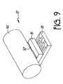
- FIG. 9is a perspective view showing an optical module of the present invention which includes a Gradient Index (GRIN) lens.
- GRINGradient Index
- FIG. 10is a front plan view of the optical module of FIG. 9 .
- the present inventionincludes various aspects that reduce or eliminate many of the problems associated with the prior art.
- the present inventionoffers an optical component which is prealigned in a standardized optical module.
- the optical modulecan be aligned with sub-micron precision with respect to registration features. Registration features on the module can be aligned with matching features on a substrate. This is similar to mounting an electrical component in or on a printed circuit board.
- Optical devicescan be easily fabricated by mounting prealigned optical modules in the optical “circuit board”. The prealignment of the optical component can compensate for variations between components to thereby essentially eliminate the effects of component variability.
- the prealigned optical modulesare well suited for automated fabrication of devices.
- the modulescan be fabricated in silicon using techniques which are well known in the art of silicon processing.
- any appropriate materialcan be used. Preferable materials are those which are used with existing electrical or optical components. Further, the invention can be used with active devices such as lasers, modulators, detectors, etc. Electrical conductors can be fabricated on the various layers for coupling to active optical components. Electrical circuitry including analog and digital circuitry, can also be fabricated directly on the modules or on the fixed reference mount.
- the present inventionprovides an optical module in which an optical component is mounted to an optical component mount.
- the optical component mountis fixed to a relative reference mount such as a base mounting plate at a desired position and orientation.
- the relative reference mountis coupled to a fixed reference mount such as a substrate such that the optical component is maintained at a desired position and orientation relative to the fixed reference mount.
- the optical componentcan be pre-aligned to a desired spacial reference and orientation by adjusting the optical component mount relative to the reference mount prior to fixing their relative positions. This can be used to provide general component pre-alignment as well as compensate for the variations which can arise between optical components.
- the following descriptionsets forth a number of specific examples, however, in various aspects, the present invention is not limited to the specific configurations, components or techniques set forth herein.
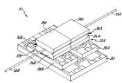
- FIG. 1is a perspective view of an optical device 10 .
- Optical device 10is shown as a simple optical fiber to optical fiber coupler for purposes of illustrating the present invention. However, the invention is applicable to more complex or other optical devices and other types of optical components.
- the optical device 10is fabricated from two optical modules 12 A and 12 B which include respective optical components 14 A and 14 B illustrated in this specific example as optical fibers.
- the fibersare mounted to respective optical component mounts 16 A and 16 B which are positioned and oriented to achieve a desired position and orientation of optical components 14 A and 14 B relative to base mounting plates 18 A and 18 B, respectively.
- base mounting plates 18 A and 18 Bcomprise substantially planar mating plates.
- Base mounting plates 18 A, 18 Bare one example of a relative reference mount.
- the relative reference mountcan have any shape or configuration.
- Base mounting plates 18 A and 18 Bmount to a reference substrate 20 such that the optical components 14 A and 14 B are in substantial alignment.
- Substrate 20is one example of a fixed reference mount and any appropriate fixed reference mount with appropriate shape and configuration can be used.
- optical component modules of the present inventioncan be pre-assembled and pre-aligned to an appropriate reference such that a final optical device is fabricated by simply mounting the assembled optical modules on the reference substrate.
- reference substrate 20is illustrated as a planar substrate which can be thought of as an optical “circuit board” which receives optical modules to form an optical, opto-electrical or opto-mechanical device.
- FIG. 2Ais an exploded perspective view of optical module 12 .
- optical component mount or holder 16comprises upper component mount or holder 24 and lower component mount or holder 26 .
- FIG. 2Aillustrates one example mounting technique coupling optical component mount 16 to base mounting plate 18 .
- a bonding material 30is carried on a top surface of base mount plate 18 .
- Material 30preferably has at least two states. In one state, material 30 does not interfere or contact mount 16 . Then, the optical component mount 16 can be positioned with up to six degrees of freedom relative to the base mounting plate 18 . In another state, the material couples mounts 16 and 18 and thereby fixes the relative position therebetween.
- material 30comprises a heat or chemically responsive (or activated) material such as solder or other bonding material.
- the soldercan comprise any type of solder including plated solder, solder. preforms, solder balls, solder paste, solder bumps, etc. including those types of solders used in flip chip electronic packages.
- other materialssuch as adhesives which dry, chemically react, or are activated by other means or other attachment techniques can be used.
- the attachment techniqueallows some relative movement between the optical component mount 16 and the base mounting plate 18 prior to fixedly attaching the two.
- heating elementssee FIG. 8B for more detail
- heating elementsare provided which are activated through the application of electrical energy through contact pads 34 . This can be by electrically contacting pads 34 and applying a current therethrough. However, other heating techniques can be used. Of course, other techniques to change the state of bonding material can be used such as application of a curing component such as radiation or a chemical. Any appropriate adhesives including brazing, welding, bonding or other technique can be used.
- the bondcan be activated using a technique including exposure to air, heat, chemicals, heat radiation (including light and UW), etc.
- FIG. 2Bis a bottom plan view of optical component mount 16 and lower mount 26 and shows bonding pads 40 which are arranged to mate with material 30 shown in FIG. 2 A.
- Pads 40can comprise, for example, a metal deposited on lower mount 26 .
- FIG. 3is a front plan view of optical module 12 showing optical component mount 16 adjacent base mounting plate 18 .
- material 30is not initially in contact with optical component mount 16 .
- material 30can be activated to fill or fix the gap 32 between mount 16 and mount 18 .
- other types of material 30can be used in which there is actual contact between mounts 16 and 18 or material 30 fills gap 32 prior to bonding.
- prior to fixedly adhering mount 16 to mount 18either component can be manipulated through up to six degrees of freedom as illustrated by the axes labeled X and Y in FIG. 3 along with another Z axis which is not shown and is perpendicular to a plane of the Figure, and rotation about the three axes.
- FIG. 3also illustrates example registration features 50 .
- each registration feature 50is a protrusion which is configured to mate with reference substrate 20 as discussed below.
- FIG. 3also shows a component registration feature 60 formed in lower component mount 26 and a component registration feature 62 in upper component mount 24 .
- component registration features 60 and 62comprise V-grooves which are configured to receive an optical component such as optical component 14 .
- the optical element 14can be coupled to the optical component mount using, for example, an adhesive or solder.
- Optical component 14is preferably fixed to component mount 16 to maintain alignment relative to registration features 50 of relative reference mount 18 .
- FIG. 4is a bottom plan view of optical module 12 which shows base mounting plate 18 and a portion of lower optical component mount 26 of optical component mount 16 . Pads 54 on base mounting plate 18 can bond with bonding material 72 .
- the bottom plan view of FIG. 4illustrates an interface surface 64 of optical component mount 16 .
- Interface surface 64is an input, output or input/output face for the optical component 14 shown in FIG. 3 .
- the interface surfaces of adjacent optical modulesare in abutting contact.
- a refractive index optical matching materialfills any gap between adjacent interface faces to provide improved coupling and reduce reflections.
- the optical matching materialmay be in a solid, gel or liquid form.
- interface surface 64is a plane which forms an angle relative to a plane perpendicular to the direction of propagation of optical fiber 14 .
- thiscan be eight degrees.
- An angled surface 64 of the optical component 14can be preferable because it reduces the amount of reflected light which is coupled back into an optical fiber. If two modules are in close proximity or in abutting contact, the adjacent optical component mount would have a complimentary angle.
- interface surface 64can be shaped or formed using an appropriate process such as a lapping process, chemically machining, machining, etc., or an additive process, to achieve the desired configuration.
- the surface 64can be lapped to achieve the desired angle or surface finish. Such techniques can also be used to ensure that a face of the optical component is flush with the interface surface 64 . However, in some embodiments, it may be desirable to have the optical component 14 either recessed or protruding from interface surface 64 .
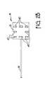
- FIG. 5is a top plan view of reference substrate 20 configured to receive optical modules 12 A and 12 B shown in FIG. 1 .
- Registration features 70 A and 70 Bare provided to receive registration features 50 on respective optical modules 12 A and 12 B.
- features 70are precisely defined depressions configured to register the protrusions of registration features 50 shown in FIGS. 3 or 4 .
- FIG. 7AThis example embodiment is shown in FIG. 7A in more detail.
- the dashed outlinesindicate the placement of base mounting plates 18 A and 18 B.
- This configurationprovides an example of a kinematic-type registration or alignment technique.
- One example kinematic techniqueis described in U.S. Pat. No. 5,748,827, entitled “TWO-STAGE KINEMATIC MOUNT”.
- a heat activated material 72such as solder is provided which can be heated to fixedly adhere the optical modules to the reference substrate.
- contact pads 74electrically couple to heaters which are used to heat material 72 .
- Material 72is preferably aligned with pads 54 shown in FIG. 4 .
- pads 54can be of a material to which material 72 will strongly adhere.
- pads 54can comprise a metal to which solder will adhere.
- Pads used to promote adhesioncan have multiple layers. For example, one layer to bond with the bonding material and another layer bond with the mount, such as mounts 16 , 18 or substrate 20 .
- FIG. 6is a cross-sectional view showing optical module 12 mounted taken along the line labeled 6 — 6 in FIG. 4 and including substrate 20 .
- This viewshows the assembled configuration in which the optical module 12 is coupled to the reference substrate 20 and component holder 16 is coupled to base mounting plate 18 .
- FIG. 7Ais an enlarged cross-sectional and FIG. 7B is an enlarged exploded view showing groove registration feature 70 and protruding registration feature 50 .
- the relative spacing between plate 18 and substrate 20can be controlled by adjusting the angle or widths of the walls of v-groove 70 or of protrusion 50 . If fabricated in properly oriented, single crystal silicon, the angle is typically fixed by the crystal structure of the material and the width can be adjusted to control the spacing. The coupling between plate 18 and substrate 20 actually occurs at line contact points 76 .
- FIG. 8Ais a perspective view showing bonding material 30 in greater detail and FIG. 8B is a cross-sectional view showing bonding material 30 between lower component mount 26 and mounting plate 18 .
- Bonding material 30is carried on heating elements 80 which are electrically coupled to conductors 82 .
- Heating elements 80can comprise a resistive elements such as a refractory metal or alloy such as tantalum, chromium or nichrome and be configured to melt material 30 when sufficient electrical current is supplied through conductors 82 .
- FIG. 8Billustrates the configuration near heating element 80 .
- FIG. 8Bis a diagram of thin film layers and is not to scale and shows features, such as contacts 34 which are remote from the heater element 80 and near the edge of mounting plate 18 .
- Element 80is shown electrically coupled to contacts 34 through electrical conductors 82 .
- An electrical insulating layer 87can optionally be positioned between element 80 and material 30 to increase the amount of electrical current flowing through element 80 .
- Additional layer or layers 85can be deposited on insulator 87 to promote adhesion or provide other characteristics or qualities as desired.
- Thermal (and/or electrical) isolation layers 89can also be applied to reduce the transfer of thermal energy to the surrounding components.
- heating element 80is designed to operate in a thermally adiabatic regime. As current flows through the heating element 80 and it begins to warm, the thermal energy flows into the bonding material 30 .
- the structurepreferably is configured to reduce heat flow into the surrounding areas. This reduces the energy required to activate the bonding material, reduces the heating and setting times and reduces the thermal stress applied to the surrounding material.
- Element 80can have any appropriate shape including straight, bifilar, serpentine, etc. Solder provides a bonding material which can be quickly attached (in less than 100 mSec) and allows “reworking” the bond by reheating the solder.
- the various materialscan be selected as desired for the appropriate physical properties. SiO 2 provides good thermal and electrical isolation and is easily processed. Of course, other materials including other oxides or organic films can be used.
- the electrical isolation layer 87is preferably relatively thin and provides high thermal conductivity. Silicon nitride is one example material.
- the conductors 82can be any conductive material however, preferable materials include those which are easily deposited such as thick refractory metals, gold or aluminum.
- the material or materials for pads 54can be any appropriate material which adheres to the bonding material 30 . Examples include, titanium, gold, nickel, etc. The thickness of the various layers should also be selected to reduce the thermal load on the heating element. Pad 54 is shown with layers 54 A and 54 B.
- Layers 54 Acan be of a material suitable for bonding to thermal isolation layer 89 .
- Niif layer 89 is SiO 2 .
- Layer 54 Bis configured to bond with bonding material 30 and may be, for example, gold, nickel, titanium, or other materials.
- material 30comprises a solder formed with a large surface area region 84 and a tapered region 86 .
- surface tensioncauses the liquid material from tapered region 86 to flow toward large surface area region 84 and cause large surface area region 84 to expand in an upward direction as illustrated in FIG. 8 D.
- This configurationis advantageous because it allows the orientation of component mount 16 to be adjusted as desired (through the six degrees of freedom as discussed with respect to FIG. 3) without any interference from the bonding material 30 . Bonding material only contacts the two surfaces when heat is applied and the material fills the gap between the two components.
- plate 18can be securely registered within feature 70 prior to application of the bonding material 72 or actuation of heating elements.
- solder flow techniqueis described in U.S. Pat. No. 5,892,179, entitled “SOLDER BUMPS AND STRUCTURES FOR INTEGRATED REDISTRIBUTION ROUTING CONDUCTORS”, issued Apr. 6, 1999 which is incorporated herein by reference.
- the bonding techniquecan advantageously use the surface tension developed in the bonding material.
- the solder or adhesivecan be electrically conductive to provide electrical contacts to the optical device between the various layers, or to adjacent electronic circuitry.
- Thermally conductive materialscan be used to help dissipate heat.
- two bonding materialsare used, which can be the same or different and can be applied simultaneously or sequentially. For example, after the solder discussed herein is applied, a second bonding material can fill the gap to provide additional stability. However, shrinkage or other shape changes of the bonding material should be addressed to maintain alignment.
- roughness or texturing the surfaces using any appropriate techniquecan be used to promote adhesion of the bonding material.
- Component 14can be any type of optical opto-electrical or opto-mechanical element including active or passive elements.
- optical element 14is shown as an optical fiber.
- an optical element 90is shown which comprises a GRIN lens.
- FIG. 9is a perspective view showing lens 90 held in component mount 16 which coupled to base mounting plate 18 .
- FIG. 10is a front plan view. Lens 90 is registered with a registration groove 60 . Additional support bonding material 92 is provided to secure lens 90 to component mount 16 . This can be an adhesive, solder or other bonding material.
- the various componentscan be fabricated using any appropriate technique or material.
- the depressions or grooves for various registration featuresare formed by anisotropically etching oriented single-crystal silicon.
- Protrusionscan be formed in an analogous, complimentary manner.
- the configurationshould preferably eliminate or substantially reduce movement in any of the six degrees of freedom. This is required to achieve sub-micron spacial reproducibility between components.
- a [ 100 ] orientation of single crystal siliconallows the formation of such features which can be orientated at 90 degrees to one another.
- Any appropriate etching or formation techniquecan be used.
- One common anisotropic etch techniqueuses KOH and masking to define the desired features.
- any appropriate sputtering, plating, evaporation or other fabrication techniquecan be used.
- optical moduleswhich can reduce or eliminate the effects of component variability.
- thisis achieved by adjusting the component mount (holder) relative to a registration feature on the base mounting plate.
- the bonding materialfixes the spacial orientation between the component and registration feature.
- Precise registration featuresare provided on the base mounting plate 18 such that it can be inserted into an optical “circuit board” to fabricate devices which comprise multiple optical component modules.
- the optical modulesare well suited for automated assembly of optical devices because they are in standardized packages, prealigned and can be easily mounted on a reference substrate.
- Optical modulescan be manually placed into the optical “circuit board” or the process can be automated.
- the particular optical modulesare preferably standardized to facilitate such automation.
- this configurationallows assembly of devices in a “top downward” fashion in which optical modules are moved downward into an optical “circuit board” which facilitates process automation. Further, because different modules are fabricated using similar materials, variations due to thermal expansion will affect all modules in a similar way such that the alignment between adjacent modules on the optical “circuit board” is maintained.
- solder bondcan be used advantageously to provide an electrical connection to electrical components on the module.
- the soldercan be heated in any order or combination including simultaneously.
- the position and sequence of the heating of the soldercan be configured to reduce or compensate for deformation in the components including thermal deformation.
- Soldercan also be used advantageously because the solder can be reheated allowing the component to be repositioned, removed, replaced, and/or repaired.
- the present inventionprovides an optical module in which optical variations due to component variability are eliminated or significantly reduced. This provides uniformity across multiple optical modules which is particularly desirable for automated assembly.
- the inventioncan be viewed as providing three stages of alignment between the optical component and the optical component mount. A first stage of alignment is provided between the component mount (holder) and the optical component, for example using a V-groove registration feature as shown or other technique. A second stage of alignment is between the optical component mount and registration features of the relative reference mount. This also eliminates or reduces alignment variations due to component variability. A final alignment occurs between the optical module and the reference substrate.
- the optical elementhas an optical characteristic which varies in space relative to at least one dimension.
- the optical componentis aligned with reference features on the relative reference mount by fixing the position of the component mount relative to the registration features of the relative reference mount to thereby align the optical characteristic.
- the first stage of alignmentis eliminated and the optical element is directly aligned with the registration features of the relative reference mount and no mount/holder is used.
- the optical componentcan be any type of active or passive optical, opto-electrical or opto-mechanical component and not limited to the specific examples set forth herein.
- the optical componentcan be aligned and its orientation fixed using any suitable or desirable means.
- the relative reference mount and other componentsare formed from a single crystal material such as silicon.
- these componentscan be fabricated from any electrical material including semiconductors or ceramics.
- Other materialsinclude machinable materials such as steel, aluminum, metal alloys, etc. depending on requirements of a particular implementation.
- An assembled optical modulecan be used to fabricate an optical device using a “pick and place” machine or any suitable or desirable means.
- the chamfers or bevels on the edges of the component mountcan facilitate mechanical gripping of the mount.
- the various components of the inventioncan be fabricated using any desired technique. Solders are known in the art and any appropriate solder can be selected to obtain the desired characteristics.
- the optical componentcan be coupled directly to the relative reference mount without a separate component mount.
- “light”is not necessarily visible light.
- the optical componentcan be any active or passive optical, opto-electrical or opto-mechanical element.
- the optical modulescan be prealigned using any appropriate technique for example, the techniques set forth in U.S. Pat. application Ser. No. 09/789,317, filed Feb. 20, 2001 and entitled “OPTICAL ALIGNMENT SYSTEM”. In an example alternative, the alignment is performed insitu, after the optical module or relative reference mount has been mounted to the optical “circuit board”.
Landscapes
- Physics & Mathematics (AREA)
- General Physics & Mathematics (AREA)
- Optics & Photonics (AREA)
- Engineering & Computer Science (AREA)
- Plasma & Fusion (AREA)
- Optical Couplings Of Light Guides (AREA)
Abstract
Description
Claims (64)
Priority Applications (20)
| Application Number | Priority Date | Filing Date | Title |
|---|---|---|---|
| US09/789,125US6546173B2 (en) | 2001-02-20 | 2001-02-20 | Optical module |
| US09/920,366US6956999B2 (en) | 2001-02-20 | 2001-08-01 | Optical device |
| CN 02805258CN1220086C (en) | 2001-02-20 | 2002-02-20 | Optical module |
| AU2002306580AAU2002306580A1 (en) | 2001-02-20 | 2002-02-20 | Optical circuit pick and place machine |
| PCT/US2002/005498WO2002067034A2 (en) | 2001-02-20 | 2002-02-20 | Optical circuit pick and place machine |
| GB0319380AGB2387923B (en) | 2001-02-20 | 2002-02-20 | Optical device |
| PCT/US2002/005497WO2002067033A2 (en) | 2001-02-20 | 2002-02-20 | Optical module |
| PCT/US2002/005412WO2002075415A2 (en) | 2001-02-20 | 2002-02-20 | Optical device |
| GB0319381AGB2390174B (en) | 2001-02-20 | 2002-02-20 | Opticle module |
| AU2002306579AAU2002306579A1 (en) | 2001-02-20 | 2002-02-20 | Optical module |
| AU2002240468AAU2002240468A1 (en) | 2001-02-20 | 2002-02-20 | Optical device |
| CN 02805259CN1259585C (en) | 2001-02-20 | 2002-02-20 | Optical device |
| PCT/US2002/005268WO2002067032A2 (en) | 2001-02-20 | 2002-02-20 | Optical alignment system |
| AU2002252056AAU2002252056A1 (en) | 2001-02-20 | 2002-02-20 | Optical alignment system |
| US10/099,920US20020181897A1 (en) | 2001-02-20 | 2002-03-15 | Optical module with electrical signal routing |
| US10/099,907US20020154870A1 (en) | 2001-02-20 | 2002-03-15 | Optical module with heat dissipation |
| US10/098,743US20020168147A1 (en) | 2001-02-20 | 2002-03-15 | Optical circuit pick and place machine |
| US10/352,798US7010855B2 (en) | 2001-02-20 | 2003-01-28 | Optical module |
| US10/420,349US20040212802A1 (en) | 2001-02-20 | 2003-04-22 | Optical device with alignment compensation |
| US11/181,530US7369334B2 (en) | 2001-02-20 | 2005-07-14 | Optical device with alignment compensation |
Applications Claiming Priority (1)
| Application Number | Priority Date | Filing Date | Title |
|---|---|---|---|
| US09/789,125US6546173B2 (en) | 2001-02-20 | 2001-02-20 | Optical module |
Related Parent Applications (1)
| Application Number | Title | Priority Date | Filing Date |
|---|---|---|---|
| US09/789,185Continuation-In-PartUS6443631B1 (en) | 2001-02-20 | 2001-02-20 | Optical module with solder bond |
Related Child Applications (6)
| Application Number | Title | Priority Date | Filing Date |
|---|---|---|---|
| US09/789,124Continuation-In-PartUS6546172B2 (en) | 2001-02-20 | 2001-02-20 | Optical device |
| US09/920,366Continuation-In-PartUS6956999B2 (en) | 2001-02-20 | 2001-08-01 | Optical device |
| US10/099,920Continuation-In-PartUS20020181897A1 (en) | 2001-02-20 | 2002-03-15 | Optical module with electrical signal routing |
| US10/099,907Continuation-In-PartUS20020154870A1 (en) | 2001-02-20 | 2002-03-15 | Optical module with heat dissipation |
| US10/098,743Continuation-In-PartUS20020168147A1 (en) | 2001-02-20 | 2002-03-15 | Optical circuit pick and place machine |
| US10/352,798DivisionUS7010855B2 (en) | 2001-02-20 | 2003-01-28 | Optical module |
Publications (2)
| Publication Number | Publication Date |
|---|---|
| US20020114586A1 US20020114586A1 (en) | 2002-08-22 |
| US6546173B2true US6546173B2 (en) | 2003-04-08 |
Family
ID=25146662
Family Applications (2)
| Application Number | Title | Priority Date | Filing Date |
|---|---|---|---|
| US09/789,125Expired - LifetimeUS6546173B2 (en) | 2001-02-20 | 2001-02-20 | Optical module |
| US10/352,798Expired - Fee RelatedUS7010855B2 (en) | 2001-02-20 | 2003-01-28 | Optical module |
Family Applications After (1)
| Application Number | Title | Priority Date | Filing Date |
|---|---|---|---|
| US10/352,798Expired - Fee RelatedUS7010855B2 (en) | 2001-02-20 | 2003-01-28 | Optical module |
Country Status (1)
| Country | Link |
|---|---|
| US (2) | US6546173B2 (en) |
Cited By (12)
| Publication number | Priority date | Publication date | Assignee | Title |
|---|---|---|---|---|
| US20020084565A1 (en)* | 2000-08-07 | 2002-07-04 | Dautartas Mindaugas F. | Alignment apparatus and method for aligning stacked devices |
| US20030077051A1 (en)* | 2001-10-22 | 2003-04-24 | Agilent Technologies, Inc. | Method for alignment of optical components |
| US20030122263A1 (en)* | 2001-12-27 | 2003-07-03 | Jun Su | Flip-chip opto-electronic circuit |
| US20030219210A1 (en)* | 2001-02-20 | 2003-11-27 | Case Steven K. | Optical module |
| US20040001674A1 (en)* | 2001-02-20 | 2004-01-01 | Case Steven K. | Optical device |
| US20040018660A1 (en)* | 2002-07-27 | 2004-01-29 | Kim Su Hyeon | Method of fabricating multilayered UBM for flip chip interconnections by electroplating |
| US20040212802A1 (en)* | 2001-02-20 | 2004-10-28 | Case Steven K. | Optical device with alignment compensation |
| US20050201689A1 (en)* | 2004-03-11 | 2005-09-15 | Moti Margalit | Method of coupling fiber to waveguide |
| US20050201668A1 (en)* | 2004-03-11 | 2005-09-15 | Avi Neta | Method of connecting an optical element at a slope |
| US20050201667A1 (en)* | 2004-03-11 | 2005-09-15 | Avi Neta | Method of connecting an optical element to a PLC |
| US20080018000A1 (en)* | 2005-10-03 | 2008-01-24 | Krishnamoorthy Ashok V | Method and apparatus for precisely aligning integrated circuit chips |
| US20150155674A1 (en)* | 2010-07-21 | 2015-06-04 | Japan Aviation Electronics Industry, Limited | Connector, method of manufacturing the connector and apparatus for manufacturing the connector |
Families Citing this family (3)
| Publication number | Priority date | Publication date | Assignee | Title |
|---|---|---|---|---|
| US9635794B2 (en)* | 2012-02-20 | 2017-04-25 | Trw Automotive U.S. Llc | Method and apparatus for attachment of integrated circuits |
| KR102067595B1 (en)* | 2015-07-23 | 2020-01-17 | 피니사 코포레이숀 | Parts alignment |
| EP3977188A1 (en)* | 2019-05-29 | 2022-04-06 | Alcon Inc. | Optical component mounting system |
Citations (94)
| Publication number | Priority date | Publication date | Assignee | Title |
|---|---|---|---|---|
| JPS5412286A (en) | 1977-06-28 | 1979-01-29 | Toshiba Corp | Semiconductor device |
| US4250520A (en) | 1979-03-14 | 1981-02-10 | Rca Corporation | Flip chip mounted diode |
| US4457467A (en) | 1981-09-25 | 1984-07-03 | Siemens Aktiengesellschaft | Method for positioning and fixing optical components relative to one another |
| US4708429A (en) | 1985-09-26 | 1987-11-24 | Rca Corporation | Optical fiber assembly and optically coupled device package including same |
| JPS62276890A (en) | 1986-05-26 | 1987-12-01 | Hitachi Ltd | Electronic component |
| US4720163A (en) | 1985-06-28 | 1988-01-19 | Northern Telecom Limited | Laser-fiber positioner |
| JPS6312187A (en) | 1986-07-03 | 1988-01-19 | Matsushita Electric Ind Co Ltd | semiconductor laser equipment |
| US4730198A (en) | 1984-11-26 | 1988-03-08 | American Telephone And Telegraph Company, At&T Bell Laboratories | Aligning arrays of optoelectronic devices to arrays of optical fibers |
| JPS6365411A (en) | 1986-09-08 | 1988-03-24 | Matsushita Electric Ind Co Ltd | Lens fixing method |
| US4750799A (en) | 1984-08-10 | 1988-06-14 | Nippon Telegraph And Telephone Corporation | Hybrid optical integrated circuit |
| US4752816A (en) | 1983-04-05 | 1988-06-21 | Plessey Overseas Limited | Electronic component |
| JPS63193113A (en) | 1987-02-06 | 1988-08-10 | Oki Electric Ind Co Ltd | Semiconductor laser optical fiber coupling device |
| JPS63228113A (en) | 1987-02-25 | 1988-09-22 | シーメンス、アクチエンゲゼルシヤフト | Optical coupling device and its manufacturing method |
| US4790618A (en) | 1985-11-01 | 1988-12-13 | Nec Corporation | Semiconductor laser module |
| US4798439A (en) | 1985-03-29 | 1989-01-17 | British Telecommunications, Plc | Optical component mounting |
| US4817849A (en) | 1986-09-09 | 1989-04-04 | Matsushita Electric Industrial Co., Ltd. | Method for bonding semiconductor laser element and apparatus therefor |
| US4845052A (en) | 1986-02-07 | 1989-07-04 | Harris Corporation | Method of packaging a non-contact I/O signal transmission integrated circuit |
| US4854667A (en) | 1987-10-30 | 1989-08-08 | Japan Aviation Electronics Industry Limited | Optical fiber alignment and fixing method and apparatus therefor |
| JPH01302214A (en) | 1988-05-30 | 1989-12-06 | Sumitomo Electric Ind Ltd | chip carrier |
| US4892377A (en) | 1987-08-19 | 1990-01-09 | Plessey Overseas Limited | Alignment of fibre arrays |
| US4909590A (en) | 1987-01-09 | 1990-03-20 | The Furukawa Electric Co., Ltd. | Method and apparatus for switching optical connector |
| US4954458A (en) | 1982-06-03 | 1990-09-04 | Texas Instruments Incorporated | Method of forming a three dimensional integrated circuit structure |
| US4989934A (en) | 1987-11-13 | 1991-02-05 | Kopin Corporation | Monolithic integrated transceiver of III-V devices on silicon |
| US5093879A (en) | 1990-06-22 | 1992-03-03 | International Business Machines Corporation | Electro-optical connectors |
| US5113404A (en) | 1990-07-05 | 1992-05-12 | At&T Bell Laboratories | Silicon-based optical subassembly |
| US5123074A (en) | 1988-02-26 | 1992-06-16 | Fujitsu Limited | Substrate for mounting optical components and electric circuit components thereon and method for making same |
| US5170455A (en) | 1991-10-30 | 1992-12-08 | At&T Bell Laboratories | Optical connective device |
| US5177807A (en) | 1990-10-19 | 1993-01-05 | Thomson Hybrides | Device for the alignment of an optical fiber and an optoelectronic component |
| US5210811A (en) | 1990-10-19 | 1993-05-11 | Thomson Hybrides | Method for the alignment of the optical axes of an optical fiber and of an optoelectronic component, and device obtained by this method |
| US5216729A (en) | 1991-11-18 | 1993-06-01 | Harmonic Lightwaves, Inc. | Active alignment system for laser to fiber coupling |
| US5215489A (en) | 1991-04-09 | 1993-06-01 | Mitsubishi Denki Kabushiki Kaisha | Method of making an optical semiconductor element module |
| US5247597A (en) | 1992-03-25 | 1993-09-21 | International Business Machines Corporation | Optical fiber alignment |
| US5249733A (en) | 1992-07-16 | 1993-10-05 | At&T Bell Laboratories | Solder self-alignment methods |
| US5283446A (en) | 1991-08-30 | 1994-02-01 | Nec Corporation | Compact optical semiconductor module capable of being readily assembled with a high precision |
| JPH0634852A (en) | 1992-07-15 | 1994-02-10 | Nec Corp | Simple optical coupling method for semiconductor laser and its device |
| US5322463A (en) | 1993-04-02 | 1994-06-21 | At&T Bell Laboratories | Process and apparatus for assembling a laser |
| US5371822A (en) | 1992-06-09 | 1994-12-06 | Digital Equipment Corporation | Method of packaging and assembling opto-electronic integrated circuits |
| US5383118A (en) | 1992-09-23 | 1995-01-17 | At&T Corp. | Device alignment methods |
| US5450508A (en) | 1994-12-08 | 1995-09-12 | International Business Machines Corporation | Apparatus and method for optical fiber alignment using adaptive feedback control loop |
| US5499312A (en) | 1993-11-09 | 1996-03-12 | Hewlett-Packard Company | Passive alignment and packaging of optoelectronic components to optical waveguides using flip-chip bonding technology |
| US5535296A (en) | 1994-09-28 | 1996-07-09 | Optobahn Corporation | Integrated optoelectronic coupling and connector |
| US5550088A (en) | 1993-06-02 | 1996-08-27 | Lucent Technologies Inc. | Fabrication process for a self-aligned optical subassembly |
| US5555333A (en) | 1993-07-12 | 1996-09-10 | Ricoh Company, Ltd. | Optical module and a fabrication process thereof |
| US5559914A (en) | 1993-10-19 | 1996-09-24 | Matsushita Electric Industrial Co., Ltd. | Components for optical circuits and method of manufacturing the same |
| US5570184A (en) | 1994-12-07 | 1996-10-29 | Lucent Technologies Inc. | Method and apparatus for locating the position of lasing gaps for precise alignment and placement of optoelectric components |
| US5568892A (en) | 1994-06-16 | 1996-10-29 | Lucent Technologies Inc. | Alignment and bonding techniques |
| US5574561A (en) | 1994-12-22 | 1996-11-12 | The Whitaker Corporation | Kinematic mounting of optical and optoelectronic elements on silicon waferboard |
| US5603870A (en) | 1993-02-22 | 1997-02-18 | Lucent Technologies Inc. | Optical fiber connector techniques |
| US5625733A (en) | 1995-02-09 | 1997-04-29 | Lucent Technologies Inc. | Arrangement for interconnecting an optical fiber to an optical component |
| US5644668A (en) | 1991-12-06 | 1997-07-01 | E-Systems, Inc. | High speed electro-optical signal translator |
| US5647044A (en) | 1995-12-22 | 1997-07-08 | Lucent Technologies Inc. | Fiber waveguide package with improved alignment means |
| US5659641A (en) | 1995-12-22 | 1997-08-19 | Corning, Inc. | Optical circuit on printed circuit board |
| US5671315A (en) | 1994-03-09 | 1997-09-23 | Fujitsu Limited | Optical parts fixing apparatus and method of manufacturing the same |
| US5677973A (en) | 1994-07-01 | 1997-10-14 | Hitachi Cable Co., Ltd. | Method of aligning optical fiber to optical fiber or optical fiber to optical element at junction and optical fiber array |
| US5721797A (en) | 1996-05-28 | 1998-02-24 | Lucent Technologies Inc. | Apparatus and method for mounting a laser to a substrate and aligning the laser with an optical conduit |
| US5737467A (en) | 1994-12-13 | 1998-04-07 | Hitachi, Ltd. | Resin molded optical assembly |
| US5745624A (en) | 1996-08-23 | 1998-04-28 | The Boeing Company | Automatic alignment and locking method and apparatus for fiber optic module manufacturing |
| DE19644758A1 (en) | 1996-10-29 | 1998-04-30 | Sel Alcatel Ag | Centering arrangement for positioning micro-structured bodies |
| US5748827A (en) | 1996-10-23 | 1998-05-05 | University Of Washington | Two-stage kinematic mount |
| US5748822A (en) | 1995-07-10 | 1998-05-05 | Fujitsu Limited | Optical module for connecting optical element and optical fiber |
| EP0840154A1 (en) | 1996-11-05 | 1998-05-06 | Nec Corporation | Structure for mounting an optical device |
| US5778120A (en) | 1995-05-12 | 1998-07-07 | Matsushita Electric Industrial Co., Ltd. | Optical module and method for manufacturing the optical modules |
| US5833202A (en) | 1994-11-15 | 1998-11-10 | Leica Ag | Mechanical fastening system for modular micro-optical elements |
| US5854867A (en) | 1996-10-29 | 1998-12-29 | Electronics And Telecommunications Research Institute | Optical module having lenses aligned on lens-positioning V-groove and fabrication method thereof |
| US5883988A (en) | 1996-05-13 | 1999-03-16 | Fujitsu Limited | Optical module including a photoreception device |
| US5892179A (en) | 1995-04-05 | 1999-04-06 | Mcnc | Solder bumps and structures for integrated redistribution routing conductors |
| US5894657A (en) | 1994-12-08 | 1999-04-20 | Matsushita Electric Industrial Co., Ltd. | Mounting apparatus for electronic component |
| US5898806A (en) | 1991-11-07 | 1999-04-27 | Nec Corporation | Optical interconnection circuit structure |
| US5907649A (en) | 1994-09-26 | 1999-05-25 | Siemens Aktiengesellschaft | Coupling arrangement for optically coupling together an OEIC module and optical fibers |
| US5916458A (en) | 1995-08-31 | 1999-06-29 | Fujitsu Limited | Production of optical module assembly |
| US5966486A (en) | 1996-08-29 | 1999-10-12 | The Whitaker Corporation | Tilted notched for passive optical alignment |
| US5970200A (en) | 1997-03-21 | 1999-10-19 | Kabushiki Kaisha Toshiba | Apparatus having optical components and a manufacturing method thereof |
| US5985086A (en) | 1996-02-08 | 1999-11-16 | Northern Telecom Limited | Securing an optical fibre in a V-groove |
| FR2779536A1 (en) | 1998-06-09 | 1999-12-10 | Commissariat Energie Atomique | ASSEMBLY FOR CONNECTING OPTICAL FIBERS WITH OPTICAL OR OPTOELECTRONIC COMPONENTS AND METHOD FOR MANUFACTURING THE ASSEMBLY |
| US6010251A (en) | 1996-03-25 | 2000-01-04 | Mitsubishi Denki Kabushiki Kaisha | Laser diode modules converging parts, and optical coupling methods |
| EP0977061A2 (en) | 1998-07-28 | 2000-02-02 | Japan Aviation Electronics Industry, Limited | Optical waveguide device and method of producing the same |
| US6027254A (en) | 1993-08-09 | 2000-02-22 | Nippon Telegraph And Telephone Corporation | Opto-electronic hybrid integration platform, optical sub-module, opto-electronic hybrid integration circuit, and process for fabricating platform |
| US6027253A (en) | 1995-08-24 | 2000-02-22 | Ngk Insulators, Ltd. | Optical fiber array |
| US6074103A (en) | 1996-10-15 | 2000-06-13 | Sdl, Inc. | Aligning an optical fiber with electroluminescent semiconductor diodes and other optical components |
| US6106161A (en) | 1998-09-15 | 2000-08-22 | Lucent Technologies, Inc. | Optical sub-assembly package mount |
| US6112001A (en) | 1997-07-30 | 2000-08-29 | Kyocera Corporation | Optical coupler and a method of producing it |
| US6115515A (en) | 1907-09-19 | 2000-09-05 | Nec Corporation | Optical device mounting board |
| US6118917A (en) | 1997-07-31 | 2000-09-12 | Samsung Electronics Co., Ltd. | Optical fiber passive alignment apparatus using alignment platform |
| US6130448A (en) | 1998-08-21 | 2000-10-10 | Gentex Corporation | Optical sensor package and method of making same |
| US6132106A (en) | 1997-11-25 | 2000-10-17 | Nec Corporation | Optical coupling module |
| US6148511A (en) | 1998-03-12 | 2000-11-21 | Juki Corporation | Electronic component mounting machine and method therefor |
| US6151173A (en) | 1996-12-13 | 2000-11-21 | Commissariat A L'energie Atomique | Assembly of optical components optically aligned and method for making this assembly |
| US6157050A (en) | 1997-09-25 | 2000-12-05 | Sumitomo Electric Industries, Ltd. | Optical module and lead frame for optical module |
| US6155515A (en) | 1996-06-13 | 2000-12-05 | Doerfel; G. Walter | Core-insertion device for a winding machine |
| US6160936A (en) | 1997-01-19 | 2000-12-12 | Samsung Electronics Co., Ltd. | Apparatus and method for combining optical waveguide and optical fiber |
| US6164837A (en) | 1998-12-30 | 2000-12-26 | Mcdonnell Douglas Corporation | Integrated microelectromechanical alignment and locking apparatus and method for fiber optic module manufacturing |
| US6222579B1 (en) | 1999-05-14 | 2001-04-24 | Presstek, Inc. | Alignment of laser imaging assembly |
| US20010010743A1 (en) | 2000-02-02 | 2001-08-02 | Ian Cayrefourcq | Passive alignment using slanted wall pedestal |
| US6327407B1 (en) | 1997-11-07 | 2001-12-04 | Matsushita Electric Industrial Co., Ltd. | Semiconductor light-receiving device, method of manufacturing the same, bidirectional optical semiconductor device, and optical transmission system |
Family Cites Families (43)
| Publication number | Priority date | Publication date | Assignee | Title |
|---|---|---|---|---|
| US894872A (en)* | 1907-06-18 | 1908-08-04 | Sherman Armstrong | Meat-tenderer. |
| DE2159327C3 (en) | 1971-11-30 | 1975-03-20 | Licentia Patent-Verwaltungs-Gmbh, 6000 Frankfurt | Device for adjusting two optical components |
| DE2358785C2 (en) | 1973-11-26 | 1983-04-21 | Licentia Patent-Verwaltungs-Gmbh, 6000 Frankfurt | Adjustable coupling device for optical components |
| JPS5412286Y2 (en) | 1975-06-16 | 1979-05-30 | ||
| JPS58165388U (en) | 1982-04-28 | 1983-11-04 | 日本ソイル工業株式会社 | Pipe positioning structure |
| JPS60257943A (en) | 1984-06-04 | 1985-12-19 | Agency Of Ind Science & Technol | Formation of hardly workable high-strength material |
| US4741796A (en) | 1985-05-29 | 1988-05-03 | Siemens Aktiengesellschaft | Method for positioning and bonding a solid body to a support base |
| EP0222072B1 (en) | 1985-10-11 | 1993-12-15 | Hitachi, Ltd. | Method of loading surface mounted device and an apparatus therefor |
| US4752109A (en) | 1986-09-02 | 1988-06-21 | Amp Incorporated | Optoelectronics package for a semiconductor laser |
| FR2605418B1 (en) | 1986-10-17 | 1990-04-20 | Thomson Semiconducteurs | MODULE FOR COUPLING BETWEEN A SEMICONDUCTOR DEVICE AND AN OPTICAL FIBER, AND METHOD FOR ALIGNING THE SEMICONDUCTOR DEVICE AND THE FIBER |
| US4745681A (en) | 1987-04-22 | 1988-05-24 | International Business Machines Corporation | Controlled pin insertion using airflow sensing and active feedback |
| JPS63193113U (en) | 1987-05-30 | 1988-12-13 | ||
| JPH0634852Y2 (en) | 1987-11-06 | 1994-09-14 | 誠一 北林 | The head of the acupressure container |
| US4856865A (en) | 1988-01-19 | 1989-08-15 | Minnesota Mining And Manufacturing Company | Tunable splice for fiber optics |
| DE3904172A1 (en) | 1989-02-11 | 1990-08-16 | Wabco Westinghouse Fahrzeug | VALVE LAMPS |
| US5093984A (en) | 1990-05-18 | 1992-03-10 | Aehr Test Systems | Printed circuit board loader/unloader |
| US5023881A (en) | 1990-06-19 | 1991-06-11 | At&T Bell Laboratories | Photonics module and alignment method |
| US5251266A (en) | 1990-08-27 | 1993-10-05 | Sierra Research And Technology, Inc. | System for placement and mounting of fine pitch integrated circuit devices using a split mirror assembly |
| US5235407A (en) | 1990-08-27 | 1993-08-10 | Sierra Research And Technology, Inc. | System for placement and mounting of fine pitch integrated circuit devices |
| WO1993007659A1 (en) | 1991-10-09 | 1993-04-15 | Ifax Corporation | Direct integrated circuit interconnection system |
| ES2136063T3 (en)* | 1991-11-25 | 1999-11-16 | Corning Inc | METHOD TO MANUFACTURE AND SUBMIT INTEGRATED OPTICAL COMPONENTS TO TEST. |
| US5195707A (en) | 1992-05-12 | 1993-03-23 | Ignatuk Wayne R | Optic positioning device |
| US5337398A (en) | 1992-11-30 | 1994-08-09 | At&T Bell Laboratories | Single in-line optical package |
| JPH06174943A (en) | 1992-12-04 | 1994-06-24 | Toshiba Corp | Mounting for optical fiber |
| JPH06201921A (en) | 1992-12-28 | 1994-07-22 | Hitachi Cable Ltd | Optical parts and its fixing method |
| JPH06331840A (en) | 1993-05-26 | 1994-12-02 | Hitachi Cable Ltd | Optical module |
| US5416872A (en) | 1993-07-06 | 1995-05-16 | At&T Corp. | Arrangement for interconnecting an optical fiber an optoelectronic component |
| JPH07333472A (en) | 1994-06-06 | 1995-12-22 | Canon Inc | Optical component height adjustment fixing method, fixing member, and optical module incorporating optical device and optical fiber |
| US5535511A (en) | 1994-11-16 | 1996-07-16 | United Technologies Automotive, Inc. | Method of assembling a wire harness |
| US5790737A (en) | 1995-11-21 | 1998-08-04 | Mitsubishi Denki Kabushiki Kaisha | Optical semiconductor device |
| US5872880A (en) | 1996-08-12 | 1999-02-16 | Ronald S. Maynard | Hybrid-optical multi-axis beam steering apparatus |
| JP3914602B2 (en) | 1997-01-06 | 2007-05-16 | 松下電器産業株式会社 | Nozzle replacement method in electronic component mounting apparatus |
| US6396854B1 (en) | 1997-12-15 | 2002-05-28 | Mitsubishi Denki Kabushiki Kaisha | Encased semiconductor laser device in contact with a fluid and method of producing the laser device |
| US5977567A (en) | 1998-01-06 | 1999-11-02 | Lightlogic, Inc. | Optoelectronic assembly and method of making the same |
| JP3353718B2 (en) | 1998-09-14 | 2002-12-03 | 日本電気株式会社 | Optical communication module |
| US6186674B1 (en) | 1998-09-15 | 2001-02-13 | Lucent Technologies, Inc. | Optical sub-assembly package mount |
| US6392778B1 (en) | 1999-03-17 | 2002-05-21 | Koninklijke Philips Electronics N.V. | Opto-electronic element |
| US6366720B1 (en) | 1999-07-09 | 2002-04-02 | Chiaro Networks Ltd. | Integrated optics beam deflector assemblies utilizing side mounting blocks for precise alignment |
| US6470120B2 (en) | 1999-12-13 | 2002-10-22 | New Focus, Inc. | Method and apparatus for aligning fiber optics with optical elements |
| US6467972B2 (en) | 2000-02-29 | 2002-10-22 | Kyocera Corporation | Optical interconnection module |
| US6709169B2 (en) | 2000-09-28 | 2004-03-23 | Powernetix, Inc. | Thermally and mechanically stable low-cost high thermal conductivity structure for single-mode fiber coupling to laser diode |
| US6546173B2 (en) | 2001-02-20 | 2003-04-08 | Avanti Optics Corporation | Optical module |
| US6546172B2 (en) | 2001-02-20 | 2003-04-08 | Avanti Optics Corporation | Optical device |
- 2001
- 2001-02-20USUS09/789,125patent/US6546173B2/ennot_activeExpired - Lifetime
- 2003
- 2003-01-28USUS10/352,798patent/US7010855B2/ennot_activeExpired - Fee Related
Patent Citations (99)
| Publication number | Priority date | Publication date | Assignee | Title |
|---|---|---|---|---|
| US6115515A (en) | 1907-09-19 | 2000-09-05 | Nec Corporation | Optical device mounting board |
| JPS5412286A (en) | 1977-06-28 | 1979-01-29 | Toshiba Corp | Semiconductor device |
| US4250520A (en) | 1979-03-14 | 1981-02-10 | Rca Corporation | Flip chip mounted diode |
| US4457467A (en) | 1981-09-25 | 1984-07-03 | Siemens Aktiengesellschaft | Method for positioning and fixing optical components relative to one another |
| US4954458A (en) | 1982-06-03 | 1990-09-04 | Texas Instruments Incorporated | Method of forming a three dimensional integrated circuit structure |
| US4752816A (en) | 1983-04-05 | 1988-06-21 | Plessey Overseas Limited | Electronic component |
| US4750799A (en) | 1984-08-10 | 1988-06-14 | Nippon Telegraph And Telephone Corporation | Hybrid optical integrated circuit |
| US4730198A (en) | 1984-11-26 | 1988-03-08 | American Telephone And Telegraph Company, At&T Bell Laboratories | Aligning arrays of optoelectronic devices to arrays of optical fibers |
| US4798439A (en) | 1985-03-29 | 1989-01-17 | British Telecommunications, Plc | Optical component mounting |
| US4720163A (en) | 1985-06-28 | 1988-01-19 | Northern Telecom Limited | Laser-fiber positioner |
| US4708429A (en) | 1985-09-26 | 1987-11-24 | Rca Corporation | Optical fiber assembly and optically coupled device package including same |
| US4790618A (en) | 1985-11-01 | 1988-12-13 | Nec Corporation | Semiconductor laser module |
| US4845052A (en) | 1986-02-07 | 1989-07-04 | Harris Corporation | Method of packaging a non-contact I/O signal transmission integrated circuit |
| JPS62276890A (en) | 1986-05-26 | 1987-12-01 | Hitachi Ltd | Electronic component |
| JPS6312187A (en) | 1986-07-03 | 1988-01-19 | Matsushita Electric Ind Co Ltd | semiconductor laser equipment |
| JPS6365411A (en) | 1986-09-08 | 1988-03-24 | Matsushita Electric Ind Co Ltd | Lens fixing method |
| US4817849A (en) | 1986-09-09 | 1989-04-04 | Matsushita Electric Industrial Co., Ltd. | Method for bonding semiconductor laser element and apparatus therefor |
| US4909590A (en) | 1987-01-09 | 1990-03-20 | The Furukawa Electric Co., Ltd. | Method and apparatus for switching optical connector |
| JPS63193113A (en) | 1987-02-06 | 1988-08-10 | Oki Electric Ind Co Ltd | Semiconductor laser optical fiber coupling device |
| JPS63228113A (en) | 1987-02-25 | 1988-09-22 | シーメンス、アクチエンゲゼルシヤフト | Optical coupling device and its manufacturing method |
| US4892377A (en) | 1987-08-19 | 1990-01-09 | Plessey Overseas Limited | Alignment of fibre arrays |
| US4854667A (en) | 1987-10-30 | 1989-08-08 | Japan Aviation Electronics Industry Limited | Optical fiber alignment and fixing method and apparatus therefor |
| US4989934A (en) | 1987-11-13 | 1991-02-05 | Kopin Corporation | Monolithic integrated transceiver of III-V devices on silicon |
| US5123074A (en) | 1988-02-26 | 1992-06-16 | Fujitsu Limited | Substrate for mounting optical components and electric circuit components thereon and method for making same |
| JPH01302214A (en) | 1988-05-30 | 1989-12-06 | Sumitomo Electric Ind Ltd | chip carrier |
| US5093879A (en) | 1990-06-22 | 1992-03-03 | International Business Machines Corporation | Electro-optical connectors |
| US5113404A (en) | 1990-07-05 | 1992-05-12 | At&T Bell Laboratories | Silicon-based optical subassembly |
| US5177807A (en) | 1990-10-19 | 1993-01-05 | Thomson Hybrides | Device for the alignment of an optical fiber and an optoelectronic component |
| US5210811A (en) | 1990-10-19 | 1993-05-11 | Thomson Hybrides | Method for the alignment of the optical axes of an optical fiber and of an optoelectronic component, and device obtained by this method |
| US5215489A (en) | 1991-04-09 | 1993-06-01 | Mitsubishi Denki Kabushiki Kaisha | Method of making an optical semiconductor element module |
| US5283446A (en) | 1991-08-30 | 1994-02-01 | Nec Corporation | Compact optical semiconductor module capable of being readily assembled with a high precision |
| US5478778A (en) | 1991-08-30 | 1995-12-26 | Nec Corporation | Method of manufacturing a compact optical semiconductor module capable of being readily assembled with a high precision |
| US5170455A (en) | 1991-10-30 | 1992-12-08 | At&T Bell Laboratories | Optical connective device |
| US5898806A (en) | 1991-11-07 | 1999-04-27 | Nec Corporation | Optical interconnection circuit structure |
| US5216729A (en) | 1991-11-18 | 1993-06-01 | Harmonic Lightwaves, Inc. | Active alignment system for laser to fiber coupling |
| US5644668A (en) | 1991-12-06 | 1997-07-01 | E-Systems, Inc. | High speed electro-optical signal translator |
| US5247597A (en) | 1992-03-25 | 1993-09-21 | International Business Machines Corporation | Optical fiber alignment |
| US5371822A (en) | 1992-06-09 | 1994-12-06 | Digital Equipment Corporation | Method of packaging and assembling opto-electronic integrated circuits |
| JPH0634852A (en) | 1992-07-15 | 1994-02-10 | Nec Corp | Simple optical coupling method for semiconductor laser and its device |
| US5249733A (en) | 1992-07-16 | 1993-10-05 | At&T Bell Laboratories | Solder self-alignment methods |
| US5383118A (en) | 1992-09-23 | 1995-01-17 | At&T Corp. | Device alignment methods |
| US5603870A (en) | 1993-02-22 | 1997-02-18 | Lucent Technologies Inc. | Optical fiber connector techniques |
| US5322463A (en) | 1993-04-02 | 1994-06-21 | At&T Bell Laboratories | Process and apparatus for assembling a laser |
| US5550088A (en) | 1993-06-02 | 1996-08-27 | Lucent Technologies Inc. | Fabrication process for a self-aligned optical subassembly |
| US5555333A (en) | 1993-07-12 | 1996-09-10 | Ricoh Company, Ltd. | Optical module and a fabrication process thereof |
| US6027254A (en) | 1993-08-09 | 2000-02-22 | Nippon Telegraph And Telephone Corporation | Opto-electronic hybrid integration platform, optical sub-module, opto-electronic hybrid integration circuit, and process for fabricating platform |
| US5559914A (en) | 1993-10-19 | 1996-09-24 | Matsushita Electric Industrial Co., Ltd. | Components for optical circuits and method of manufacturing the same |
| US5499312A (en) | 1993-11-09 | 1996-03-12 | Hewlett-Packard Company | Passive alignment and packaging of optoelectronic components to optical waveguides using flip-chip bonding technology |
| US5671315A (en) | 1994-03-09 | 1997-09-23 | Fujitsu Limited | Optical parts fixing apparatus and method of manufacturing the same |
| US5568892A (en) | 1994-06-16 | 1996-10-29 | Lucent Technologies Inc. | Alignment and bonding techniques |
| US5700987A (en) | 1994-06-16 | 1997-12-23 | Lucent Technologies Inc. | Alignment and bonding techniques |
| US5677973A (en) | 1994-07-01 | 1997-10-14 | Hitachi Cable Co., Ltd. | Method of aligning optical fiber to optical fiber or optical fiber to optical element at junction and optical fiber array |
| US5907649A (en) | 1994-09-26 | 1999-05-25 | Siemens Aktiengesellschaft | Coupling arrangement for optically coupling together an OEIC module and optical fibers |
| US5687267A (en) | 1994-09-28 | 1997-11-11 | Optobahn Corporation | Integrated optoelectronic coupling and connector |
| US5535296A (en) | 1994-09-28 | 1996-07-09 | Optobahn Corporation | Integrated optoelectronic coupling and connector |
| US5833202A (en) | 1994-11-15 | 1998-11-10 | Leica Ag | Mechanical fastening system for modular micro-optical elements |
| US5570184A (en) | 1994-12-07 | 1996-10-29 | Lucent Technologies Inc. | Method and apparatus for locating the position of lasing gaps for precise alignment and placement of optoelectric components |
| US5450508A (en) | 1994-12-08 | 1995-09-12 | International Business Machines Corporation | Apparatus and method for optical fiber alignment using adaptive feedback control loop |
| US5894657A (en) | 1994-12-08 | 1999-04-20 | Matsushita Electric Industrial Co., Ltd. | Mounting apparatus for electronic component |
| US5737467A (en) | 1994-12-13 | 1998-04-07 | Hitachi, Ltd. | Resin molded optical assembly |
| US5574561A (en) | 1994-12-22 | 1996-11-12 | The Whitaker Corporation | Kinematic mounting of optical and optoelectronic elements on silicon waferboard |
| US5625733A (en) | 1995-02-09 | 1997-04-29 | Lucent Technologies Inc. | Arrangement for interconnecting an optical fiber to an optical component |
| US5892179A (en) | 1995-04-05 | 1999-04-06 | Mcnc | Solder bumps and structures for integrated redistribution routing conductors |
| US5778120A (en) | 1995-05-12 | 1998-07-07 | Matsushita Electric Industrial Co., Ltd. | Optical module and method for manufacturing the optical modules |
| US5859943A (en) | 1995-05-12 | 1999-01-12 | Matsushita Electric Industrial Co., Ltd. | Optical module and method for manufacturing the optical |
| US5748822A (en) | 1995-07-10 | 1998-05-05 | Fujitsu Limited | Optical module for connecting optical element and optical fiber |
| US6027253A (en) | 1995-08-24 | 2000-02-22 | Ngk Insulators, Ltd. | Optical fiber array |
| US5916458A (en) | 1995-08-31 | 1999-06-29 | Fujitsu Limited | Production of optical module assembly |
| US5647044A (en) | 1995-12-22 | 1997-07-08 | Lucent Technologies Inc. | Fiber waveguide package with improved alignment means |
| US5659641A (en) | 1995-12-22 | 1997-08-19 | Corning, Inc. | Optical circuit on printed circuit board |
| US5985086A (en) | 1996-02-08 | 1999-11-16 | Northern Telecom Limited | Securing an optical fibre in a V-groove |
| US6010251A (en) | 1996-03-25 | 2000-01-04 | Mitsubishi Denki Kabushiki Kaisha | Laser diode modules converging parts, and optical coupling methods |
| US5883988A (en) | 1996-05-13 | 1999-03-16 | Fujitsu Limited | Optical module including a photoreception device |
| US5721797A (en) | 1996-05-28 | 1998-02-24 | Lucent Technologies Inc. | Apparatus and method for mounting a laser to a substrate and aligning the laser with an optical conduit |
| US6155515A (en) | 1996-06-13 | 2000-12-05 | Doerfel; G. Walter | Core-insertion device for a winding machine |
| US5745624A (en) | 1996-08-23 | 1998-04-28 | The Boeing Company | Automatic alignment and locking method and apparatus for fiber optic module manufacturing |
| US5966486A (en) | 1996-08-29 | 1999-10-12 | The Whitaker Corporation | Tilted notched for passive optical alignment |
| US6074103A (en) | 1996-10-15 | 2000-06-13 | Sdl, Inc. | Aligning an optical fiber with electroluminescent semiconductor diodes and other optical components |
| US5748827A (en) | 1996-10-23 | 1998-05-05 | University Of Washington | Two-stage kinematic mount |
| US5854867A (en) | 1996-10-29 | 1998-12-29 | Electronics And Telecommunications Research Institute | Optical module having lenses aligned on lens-positioning V-groove and fabrication method thereof |
| DE19644758A1 (en) | 1996-10-29 | 1998-04-30 | Sel Alcatel Ag | Centering arrangement for positioning micro-structured bodies |
| EP0840154A1 (en) | 1996-11-05 | 1998-05-06 | Nec Corporation | Structure for mounting an optical device |
| US6058234A (en) | 1996-11-05 | 2000-05-02 | Nec Corporation | Structure for mounting an optical device |
| US6151173A (en) | 1996-12-13 | 2000-11-21 | Commissariat A L'energie Atomique | Assembly of optical components optically aligned and method for making this assembly |
| US6160936A (en) | 1997-01-19 | 2000-12-12 | Samsung Electronics Co., Ltd. | Apparatus and method for combining optical waveguide and optical fiber |
| US5970200A (en) | 1997-03-21 | 1999-10-19 | Kabushiki Kaisha Toshiba | Apparatus having optical components and a manufacturing method thereof |
| US6112001A (en) | 1997-07-30 | 2000-08-29 | Kyocera Corporation | Optical coupler and a method of producing it |
| US6118917A (en) | 1997-07-31 | 2000-09-12 | Samsung Electronics Co., Ltd. | Optical fiber passive alignment apparatus using alignment platform |
| US6157050A (en) | 1997-09-25 | 2000-12-05 | Sumitomo Electric Industries, Ltd. | Optical module and lead frame for optical module |
| US6327407B1 (en) | 1997-11-07 | 2001-12-04 | Matsushita Electric Industrial Co., Ltd. | Semiconductor light-receiving device, method of manufacturing the same, bidirectional optical semiconductor device, and optical transmission system |
| US6132106A (en) | 1997-11-25 | 2000-10-17 | Nec Corporation | Optical coupling module |
| US6148511A (en) | 1998-03-12 | 2000-11-21 | Juki Corporation | Electronic component mounting machine and method therefor |
| FR2779536A1 (en) | 1998-06-09 | 1999-12-10 | Commissariat Energie Atomique | ASSEMBLY FOR CONNECTING OPTICAL FIBERS WITH OPTICAL OR OPTOELECTRONIC COMPONENTS AND METHOD FOR MANUFACTURING THE ASSEMBLY |
| EP0977061A2 (en) | 1998-07-28 | 2000-02-02 | Japan Aviation Electronics Industry, Limited | Optical waveguide device and method of producing the same |
| US6130448A (en) | 1998-08-21 | 2000-10-10 | Gentex Corporation | Optical sensor package and method of making same |
| US6106161A (en) | 1998-09-15 | 2000-08-22 | Lucent Technologies, Inc. | Optical sub-assembly package mount |
| US6164837A (en) | 1998-12-30 | 2000-12-26 | Mcdonnell Douglas Corporation | Integrated microelectromechanical alignment and locking apparatus and method for fiber optic module manufacturing |
| US6222579B1 (en) | 1999-05-14 | 2001-04-24 | Presstek, Inc. | Alignment of laser imaging assembly |
| US20010010743A1 (en) | 2000-02-02 | 2001-08-02 | Ian Cayrefourcq | Passive alignment using slanted wall pedestal |
Non-Patent Citations (6)
| Title |
|---|
| "An Innovative Flexible and Accurate Packaging Technique Suited to Fabricate Low Cost Micro Optoelectronic Modules", by M. Scussat et al., Electronic Components and Technology Conference, 2000, pp. 26-32. |
| "Micro-Mechanical Alignment Structures (patent pending)", from Web Site of Axsun Technologies, 2 pages, downloaded Feb. 15, 2001. |
| Article from Web Site entitled "Automated Optoelectronic Packaging", 2 pages, downloaded Feb. 5, 2001. |
| Article from Web Site entitled "The Photonics Program and the Engineering Research Division at LLNL are Automating the Packaging of Optoelectronic Devices to Lower Costs", 3 pages, downloaded Oct. 19, 2000. |
| Article from Web Site entitled Micro Assembly Automation, 3 pages., downloaded Feb. 5, 2001. |
| U.S. patent application Ser. No. 09/894,872, filed Jun. 27, 2001, entitled "Automated Opto-Electronic Assembly Machine and Method". |
Cited By (23)
| Publication number | Priority date | Publication date | Assignee | Title |
|---|---|---|---|---|
| US20020084565A1 (en)* | 2000-08-07 | 2002-07-04 | Dautartas Mindaugas F. | Alignment apparatus and method for aligning stacked devices |
| US20060272149A1 (en)* | 2000-08-07 | 2006-12-07 | Shipley Company, L.L.C. | Alignment apparatus and method for aligning stacked devices |
| US7290321B2 (en) | 2000-08-07 | 2007-11-06 | Shipley Company, L.L.C. | Alignment apparatus and method for aligning stacked devices |
| US7086134B2 (en)* | 2000-08-07 | 2006-08-08 | Shipley Company, L.L.C. | Alignment apparatus and method for aligning stacked devices |
| US7369334B2 (en) | 2001-02-20 | 2008-05-06 | Cyberoptics Corporation | Optical device with alignment compensation |
| US20040001674A1 (en)* | 2001-02-20 | 2004-01-01 | Case Steven K. | Optical device |
| US20040212802A1 (en)* | 2001-02-20 | 2004-10-28 | Case Steven K. | Optical device with alignment compensation |
| US20030219210A1 (en)* | 2001-02-20 | 2003-11-27 | Case Steven K. | Optical module |
| US7010855B2 (en) | 2001-02-20 | 2006-03-14 | Cyberoptics Corporation | Optical module |
| US6739763B2 (en)* | 2001-10-22 | 2004-05-25 | Agilent Technologies, Inc. | Method for alignment of optical components |
| US20030077051A1 (en)* | 2001-10-22 | 2003-04-24 | Agilent Technologies, Inc. | Method for alignment of optical components |
| US6787919B2 (en)* | 2001-12-27 | 2004-09-07 | Intel Corporation | Flip-chip opto-electronic circuit |
| US20030122263A1 (en)* | 2001-12-27 | 2003-07-03 | Jun Su | Flip-chip opto-electronic circuit |
| US20040018660A1 (en)* | 2002-07-27 | 2004-01-29 | Kim Su Hyeon | Method of fabricating multilayered UBM for flip chip interconnections by electroplating |
| US7146080B2 (en) | 2004-03-11 | 2006-12-05 | Lambda Crossing, Ltd. | Method of connecting an optical element to a PLC |
| US20050201667A1 (en)* | 2004-03-11 | 2005-09-15 | Avi Neta | Method of connecting an optical element to a PLC |
| US7224870B2 (en) | 2004-03-11 | 2007-05-29 | Lambda Crossing | Method of coupling fiber to waveguide |
| US20050201668A1 (en)* | 2004-03-11 | 2005-09-15 | Avi Neta | Method of connecting an optical element at a slope |
| US20050201689A1 (en)* | 2004-03-11 | 2005-09-15 | Moti Margalit | Method of coupling fiber to waveguide |
| US20080018000A1 (en)* | 2005-10-03 | 2008-01-24 | Krishnamoorthy Ashok V | Method and apparatus for precisely aligning integrated circuit chips |
| US7619312B2 (en)* | 2005-10-03 | 2009-11-17 | Sun Microsystems, Inc. | Method and apparatus for precisely aligning integrated circuit chips |
| US20150155674A1 (en)* | 2010-07-21 | 2015-06-04 | Japan Aviation Electronics Industry, Limited | Connector, method of manufacturing the connector and apparatus for manufacturing the connector |
| US9252551B2 (en)* | 2010-07-21 | 2016-02-02 | Japan Aviation Electronics Industry, Limited | Apparatus for manufacturing a connector |
Also Published As
| Publication number | Publication date |
|---|---|
| US20030219210A1 (en) | 2003-11-27 |
| US20020114586A1 (en) | 2002-08-22 |
| US7010855B2 (en) | 2006-03-14 |
Similar Documents
| Publication | Publication Date | Title |
|---|---|---|
| US7369334B2 (en) | Optical device with alignment compensation | |
| US6546172B2 (en) | Optical device | |
| US6546173B2 (en) | Optical module | |
| US6443631B1 (en) | Optical module with solder bond | |
| EP0611142B1 (en) | A process for optically joining an optical fiber array to an opponent member | |
| US5574811A (en) | Method and apparatus for providing optical coupling between optical components | |
| EP0358592B1 (en) | Metallic bond for mounting of optical fibers to integrated optical chips | |
| JP3150662B2 (en) | Optical fiber array module with metal deposition | |
| JPH01140104A (en) | Matching of fiber array | |
| JPH0829638A (en) | Optical waveguide / optical fiber connection structure, optical waveguide / optical fiber connection method, optical waveguide substrate used for optical waveguide / optical fiber connection, method of manufacturing the same, and optical fiber with optical fiber substrate used for optical waveguide / optical fiber connection fiber | |
| KR100442609B1 (en) | Structure of flip chip bonding and method for bonding | |
| US6907178B2 (en) | Optoelectronic assembly with embedded optical and electrical components | |
| WO1998044369A1 (en) | Sealed fiber array and method for manufacturing a sealed fiber array | |
| US5297218A (en) | Optical semiconductor laser and optical waveguide alignment device | |
| WO2002075415A2 (en) | Optical device | |
| US20030235388A1 (en) | Method for fabricating fiber blocks using solder as bonding material | |
| US20020181897A1 (en) | Optical module with electrical signal routing | |
| US20020154870A1 (en) | Optical module with heat dissipation | |
| TW200304557A (en) | Ceramic waferboard | |
| US6956999B2 (en) | Optical device | |
| JP3447364B2 (en) | Optical circuit component and method of manufacturing the same | |
| JPH06118275A (en) | Optical connecting component and its manufacture | |
| JP2001272570A (en) | Optical fiber array | |
| Schmidt et al. | Laser-fiber coupling by means of a silicon micro-optical bench and a self-aligned soldering process | |
| JP3590223B2 (en) | Fabrication method of optical module |
Legal Events
| Date | Code | Title | Description |
|---|---|---|---|
| AS | Assignment | Owner name:AVANTI OPTICS CORPORATION, MINNESOTA Free format text:ASSIGNMENT OF ASSIGNORS INTEREST;ASSIGNORS:CASE, STEVEN K.;MOWRY, GREGORY S.;SKUNES, TIMOTHY A.;REEL/FRAME:011886/0014 Effective date:20010523 | |
| AS | Assignment | Owner name:CYBEROPTICS CORPORATION, MINNESOTA Free format text:SECURITY INTEREST;ASSIGNOR:AVANTI OPTICS CORPORATION;REEL/FRAME:012924/0132 Effective date:20020501 | |
| STCF | Information on status: patent grant | Free format text:PATENTED CASE | |
| AS | Assignment | Owner name:CYBEROPTICS CORPORATION, MINNESOTA Free format text:SETTLEMENT AGREEMENT;ASSIGNOR:AVANTI OPTICS CORPORATION;REEL/FRAME:013982/0973 Effective date:20030214 | |
| FEPP | Fee payment procedure | Free format text:PAT HOLDER CLAIMS SMALL ENTITY STATUS, ENTITY STATUS SET TO SMALL (ORIGINAL EVENT CODE: LTOS); ENTITY STATUS OF PATENT OWNER: LARGE ENTITY | |
| FPAY | Fee payment | Year of fee payment:4 | |
| REMI | Maintenance fee reminder mailed | ||
| FPAY | Fee payment | Year of fee payment:8 | |
| SULP | Surcharge for late payment | Year of fee payment:7 | |
| AS | Assignment | Owner name:PEAKS ISLAND LLC, DELAWARE Free format text:ASSIGNMENT OF ASSIGNORS INTEREST;ASSIGNOR:CYBEROPTICS CORPORATION;REEL/FRAME:027139/0405 Effective date:20110322 | |
| FEPP | Fee payment procedure | Free format text:PAYOR NUMBER ASSIGNED (ORIGINAL EVENT CODE: ASPN); ENTITY STATUS OF PATENT OWNER: LARGE ENTITY Free format text:PAYER NUMBER DE-ASSIGNED (ORIGINAL EVENT CODE: RMPN); ENTITY STATUS OF PATENT OWNER: LARGE ENTITY Free format text:PAT HOLDER NO LONGER CLAIMS SMALL ENTITY STATUS, ENTITY STATUS SET TO UNDISCOUNTED (ORIGINAL EVENT CODE: STOL); ENTITY STATUS OF PATENT OWNER: LARGE ENTITY | |
| AS | Assignment | Owner name:RPX CORPORATION, CALIFORNIA Free format text:ASSIGNMENT OF ASSIGNORS INTEREST;ASSIGNOR:PEAKS ISLAND LLC;REEL/FRAME:028146/0045 Effective date:20120420 | |
| FPAY | Fee payment | Year of fee payment:12 | |
| AS | Assignment | Owner name:JEFFERIES FINANCE LLC, NEW YORK Free format text:SECURITY INTEREST;ASSIGNOR:RPX CORPORATION;REEL/FRAME:046486/0433 Effective date:20180619 | |
| AS | Assignment | Owner name:BARINGS FINANCE LLC, AS COLLATERAL AGENT, NORTH CAROLINA Free format text:PATENT SECURITY AGREEMENT;ASSIGNORS:RPX CLEARINGHOUSE LLC;RPX CORPORATION;REEL/FRAME:054198/0029 Effective date:20201023 Owner name:BARINGS FINANCE LLC, AS COLLATERAL AGENT, NORTH CAROLINA Free format text:PATENT SECURITY AGREEMENT;ASSIGNORS:RPX CLEARINGHOUSE LLC;RPX CORPORATION;REEL/FRAME:054244/0566 Effective date:20200823 | |
| AS | Assignment | Owner name:RPX CORPORATION, CALIFORNIA Free format text:RELEASE BY SECURED PARTY;ASSIGNOR:JEFFERIES FINANCE LLC;REEL/FRAME:054486/0422 Effective date:20201023 |