US6545345B1 - Mounting for a package containing a chip - Google Patents
Mounting for a package containing a chipDownload PDFInfo
- Publication number
- US6545345B1 US6545345B1US09/813,485US81348501AUS6545345B1US 6545345 B1US6545345 B1US 6545345B1US 81348501 AUS81348501 AUS 81348501AUS 6545345 B1US6545345 B1US 6545345B1
- Authority
- US
- United States
- Prior art keywords
- package
- mounting
- leads
- substrate
- aperture
- Prior art date
- Legal status (The legal status is an assumption and is not a legal conclusion. Google has not performed a legal analysis and makes no representation as to the accuracy of the status listed.)
- Expired - Lifetime
Links
- 239000000758substrateSubstances0.000claimsabstractdescription72
- 239000008393encapsulating agentSubstances0.000claimsabstractdescription31
- 239000000463materialSubstances0.000claimsdescription33
- 229910052751metalInorganic materials0.000claimsdescription27
- 239000002184metalSubstances0.000claimsdescription27
- 230000002093peripheral effectEffects0.000abstractdescription10
- 239000004065semiconductorSubstances0.000abstractdescription10
- 238000000034methodMethods0.000abstractdescription3
- 229910000679solderInorganic materials0.000description7
- 239000000853adhesiveSubstances0.000description6
- 230000001070adhesive effectEffects0.000description6
- 239000004020conductorSubstances0.000description3
- 125000006850spacer groupChemical group0.000description3
- RYGMFSIKBFXOCR-UHFFFAOYSA-NCopperChemical compound[Cu]RYGMFSIKBFXOCR-UHFFFAOYSA-N0.000description2
- 239000004593EpoxySubstances0.000description2
- 239000000919ceramicSubstances0.000description2
- 229910052802copperInorganic materials0.000description2
- 239000010949copperSubstances0.000description2
- 239000003365glass fiberSubstances0.000description2
- PCHJSUWPFVWCPO-UHFFFAOYSA-NgoldChemical compound[Au]PCHJSUWPFVWCPO-UHFFFAOYSA-N0.000description2
- 229910052737goldInorganic materials0.000description2
- 239000010931goldSubstances0.000description2
- 239000010410layerSubstances0.000description2
- 230000003287optical effectEffects0.000description2
- 229910000881Cu alloyInorganic materials0.000description1
- 241000272168LaridaeSpecies0.000description1
- 229910000831SteelInorganic materials0.000description1
- 239000002313adhesive filmSubstances0.000description1
- 229910045601alloyInorganic materials0.000description1
- 239000000956alloySubstances0.000description1
- 229910052782aluminiumInorganic materials0.000description1
- XAGFODPZIPBFFR-UHFFFAOYSA-NaluminiumChemical compound[Al]XAGFODPZIPBFFR-UHFFFAOYSA-N0.000description1
- 239000003990capacitorSubstances0.000description1
- 239000012792core layerSubstances0.000description1
- 210000005069earsAnatomy0.000description1
- 239000003822epoxy resinSubstances0.000description1
- 238000005530etchingMethods0.000description1
- 230000006870functionEffects0.000description1
- 238000003780insertionMethods0.000description1
- 230000037431insertionEffects0.000description1
- 230000000873masking effectEffects0.000description1
- 239000011095metalized laminateSubstances0.000description1
- 238000000465mouldingMethods0.000description1
- 229920000647polyepoxidePolymers0.000description1
- 229920001721polyimidePolymers0.000description1
- 238000004080punchingMethods0.000description1
- 230000009467reductionEffects0.000description1
- 229920005989resinPolymers0.000description1
- 239000011347resinSubstances0.000description1
- 229910052710siliconInorganic materials0.000description1
- 239000010703siliconSubstances0.000description1
- 239000010959steelSubstances0.000description1
Images


Classifications
- H—ELECTRICITY
- H05—ELECTRIC TECHNIQUES NOT OTHERWISE PROVIDED FOR
- H05K—PRINTED CIRCUITS; CASINGS OR CONSTRUCTIONAL DETAILS OF ELECTRIC APPARATUS; MANUFACTURE OF ASSEMBLAGES OF ELECTRICAL COMPONENTS
- H05K1/00—Printed circuits
- H05K1/18—Printed circuits structurally associated with non-printed electric components
- H05K1/182—Printed circuits structurally associated with non-printed electric components associated with components mounted in the printed circuit board, e.g. insert mounted components [IMC]
- H—ELECTRICITY
- H01—ELECTRIC ELEMENTS
- H01L—SEMICONDUCTOR DEVICES NOT COVERED BY CLASS H10
- H01L23/00—Details of semiconductor or other solid state devices
- H01L23/52—Arrangements for conducting electric current within the device in operation from one component to another, i.e. interconnections, e.g. wires, lead frames
- H01L23/538—Arrangements for conducting electric current within the device in operation from one component to another, i.e. interconnections, e.g. wires, lead frames the interconnection structure between a plurality of semiconductor chips being formed on, or in, insulating substrates
- H01L23/5389—Arrangements for conducting electric current within the device in operation from one component to another, i.e. interconnections, e.g. wires, lead frames the interconnection structure between a plurality of semiconductor chips being formed on, or in, insulating substrates the chips being integrally enclosed by the interconnect and support structures
- H—ELECTRICITY
- H01—ELECTRIC ELEMENTS
- H01L—SEMICONDUCTOR DEVICES NOT COVERED BY CLASS H10
- H01L2224/00—Indexing scheme for arrangements for connecting or disconnecting semiconductor or solid-state bodies and methods related thereto as covered by H01L24/00
- H01L2224/01—Means for bonding being attached to, or being formed on, the surface to be connected, e.g. chip-to-package, die-attach, "first-level" interconnects; Manufacturing methods related thereto
- H01L2224/26—Layer connectors, e.g. plate connectors, solder or adhesive layers; Manufacturing methods related thereto
- H01L2224/31—Structure, shape, material or disposition of the layer connectors after the connecting process
- H01L2224/32—Structure, shape, material or disposition of the layer connectors after the connecting process of an individual layer connector
- H01L2224/321—Disposition
- H01L2224/32135—Disposition the layer connector connecting between different semiconductor or solid-state bodies, i.e. chip-to-chip
- H01L2224/32145—Disposition the layer connector connecting between different semiconductor or solid-state bodies, i.e. chip-to-chip the bodies being stacked
- H—ELECTRICITY
- H01—ELECTRIC ELEMENTS
- H01L—SEMICONDUCTOR DEVICES NOT COVERED BY CLASS H10
- H01L2224/00—Indexing scheme for arrangements for connecting or disconnecting semiconductor or solid-state bodies and methods related thereto as covered by H01L24/00
- H01L2224/01—Means for bonding being attached to, or being formed on, the surface to be connected, e.g. chip-to-package, die-attach, "first-level" interconnects; Manufacturing methods related thereto
- H01L2224/42—Wire connectors; Manufacturing methods related thereto
- H01L2224/44—Structure, shape, material or disposition of the wire connectors prior to the connecting process
- H01L2224/45—Structure, shape, material or disposition of the wire connectors prior to the connecting process of an individual wire connector
- H01L2224/45001—Core members of the connector
- H01L2224/45099—Material
- H01L2224/451—Material with a principal constituent of the material being a metal or a metalloid, e.g. boron (B), silicon (Si), germanium (Ge), arsenic (As), antimony (Sb), tellurium (Te) and polonium (Po), and alloys thereof
- H01L2224/45117—Material with a principal constituent of the material being a metal or a metalloid, e.g. boron (B), silicon (Si), germanium (Ge), arsenic (As), antimony (Sb), tellurium (Te) and polonium (Po), and alloys thereof the principal constituent melting at a temperature of greater than or equal to 400°C and less than 950°C
- H01L2224/45124—Aluminium (Al) as principal constituent
- H—ELECTRICITY
- H01—ELECTRIC ELEMENTS
- H01L—SEMICONDUCTOR DEVICES NOT COVERED BY CLASS H10
- H01L2224/00—Indexing scheme for arrangements for connecting or disconnecting semiconductor or solid-state bodies and methods related thereto as covered by H01L24/00
- H01L2224/01—Means for bonding being attached to, or being formed on, the surface to be connected, e.g. chip-to-package, die-attach, "first-level" interconnects; Manufacturing methods related thereto
- H01L2224/42—Wire connectors; Manufacturing methods related thereto
- H01L2224/44—Structure, shape, material or disposition of the wire connectors prior to the connecting process
- H01L2224/45—Structure, shape, material or disposition of the wire connectors prior to the connecting process of an individual wire connector
- H01L2224/45001—Core members of the connector
- H01L2224/45099—Material
- H01L2224/451—Material with a principal constituent of the material being a metal or a metalloid, e.g. boron (B), silicon (Si), germanium (Ge), arsenic (As), antimony (Sb), tellurium (Te) and polonium (Po), and alloys thereof
- H01L2224/45138—Material with a principal constituent of the material being a metal or a metalloid, e.g. boron (B), silicon (Si), germanium (Ge), arsenic (As), antimony (Sb), tellurium (Te) and polonium (Po), and alloys thereof the principal constituent melting at a temperature of greater than or equal to 950°C and less than 1550°C
- H01L2224/45144—Gold (Au) as principal constituent
- H—ELECTRICITY
- H01—ELECTRIC ELEMENTS
- H01L—SEMICONDUCTOR DEVICES NOT COVERED BY CLASS H10
- H01L2224/00—Indexing scheme for arrangements for connecting or disconnecting semiconductor or solid-state bodies and methods related thereto as covered by H01L24/00
- H01L2224/01—Means for bonding being attached to, or being formed on, the surface to be connected, e.g. chip-to-package, die-attach, "first-level" interconnects; Manufacturing methods related thereto
- H01L2224/42—Wire connectors; Manufacturing methods related thereto
- H01L2224/47—Structure, shape, material or disposition of the wire connectors after the connecting process
- H01L2224/48—Structure, shape, material or disposition of the wire connectors after the connecting process of an individual wire connector
- H01L2224/4805—Shape
- H01L2224/4809—Loop shape
- H01L2224/48091—Arched
- H—ELECTRICITY
- H01—ELECTRIC ELEMENTS
- H01L—SEMICONDUCTOR DEVICES NOT COVERED BY CLASS H10
- H01L2224/00—Indexing scheme for arrangements for connecting or disconnecting semiconductor or solid-state bodies and methods related thereto as covered by H01L24/00
- H01L2224/01—Means for bonding being attached to, or being formed on, the surface to be connected, e.g. chip-to-package, die-attach, "first-level" interconnects; Manufacturing methods related thereto
- H01L2224/42—Wire connectors; Manufacturing methods related thereto
- H01L2224/47—Structure, shape, material or disposition of the wire connectors after the connecting process
- H01L2224/48—Structure, shape, material or disposition of the wire connectors after the connecting process of an individual wire connector
- H01L2224/4805—Shape
- H01L2224/4809—Loop shape
- H01L2224/48095—Kinked
- H—ELECTRICITY
- H01—ELECTRIC ELEMENTS
- H01L—SEMICONDUCTOR DEVICES NOT COVERED BY CLASS H10
- H01L2224/00—Indexing scheme for arrangements for connecting or disconnecting semiconductor or solid-state bodies and methods related thereto as covered by H01L24/00
- H01L2224/73—Means for bonding being of different types provided for in two or more of groups H01L2224/10, H01L2224/18, H01L2224/26, H01L2224/34, H01L2224/42, H01L2224/50, H01L2224/63, H01L2224/71
- H01L2224/732—Location after the connecting process
- H01L2224/73251—Location after the connecting process on different surfaces
- H01L2224/73265—Layer and wire connectors
- H—ELECTRICITY
- H01—ELECTRIC ELEMENTS
- H01L—SEMICONDUCTOR DEVICES NOT COVERED BY CLASS H10
- H01L24/00—Arrangements for connecting or disconnecting semiconductor or solid-state bodies; Methods or apparatus related thereto
- H01L24/01—Means for bonding being attached to, or being formed on, the surface to be connected, e.g. chip-to-package, die-attach, "first-level" interconnects; Manufacturing methods related thereto
- H01L24/42—Wire connectors; Manufacturing methods related thereto
- H01L24/44—Structure, shape, material or disposition of the wire connectors prior to the connecting process
- H01L24/45—Structure, shape, material or disposition of the wire connectors prior to the connecting process of an individual wire connector
- H—ELECTRICITY
- H01—ELECTRIC ELEMENTS
- H01L—SEMICONDUCTOR DEVICES NOT COVERED BY CLASS H10
- H01L24/00—Arrangements for connecting or disconnecting semiconductor or solid-state bodies; Methods or apparatus related thereto
- H01L24/01—Means for bonding being attached to, or being formed on, the surface to be connected, e.g. chip-to-package, die-attach, "first-level" interconnects; Manufacturing methods related thereto
- H01L24/42—Wire connectors; Manufacturing methods related thereto
- H01L24/47—Structure, shape, material or disposition of the wire connectors after the connecting process
- H01L24/48—Structure, shape, material or disposition of the wire connectors after the connecting process of an individual wire connector
- H—ELECTRICITY
- H01—ELECTRIC ELEMENTS
- H01L—SEMICONDUCTOR DEVICES NOT COVERED BY CLASS H10
- H01L2924/00—Indexing scheme for arrangements or methods for connecting or disconnecting semiconductor or solid-state bodies as covered by H01L24/00
- H01L2924/01—Chemical elements
- H01L2924/01079—Gold [Au]
- H—ELECTRICITY
- H01—ELECTRIC ELEMENTS
- H01L—SEMICONDUCTOR DEVICES NOT COVERED BY CLASS H10
- H01L2924/00—Indexing scheme for arrangements or methods for connecting or disconnecting semiconductor or solid-state bodies as covered by H01L24/00
- H01L2924/10—Details of semiconductor or other solid state devices to be connected
- H01L2924/11—Device type
- H01L2924/14—Integrated circuits
- H—ELECTRICITY
- H01—ELECTRIC ELEMENTS
- H01L—SEMICONDUCTOR DEVICES NOT COVERED BY CLASS H10
- H01L2924/00—Indexing scheme for arrangements or methods for connecting or disconnecting semiconductor or solid-state bodies as covered by H01L24/00
- H01L2924/15—Details of package parts other than the semiconductor or other solid state devices to be connected
- H01L2924/181—Encapsulation
- H—ELECTRICITY
- H01—ELECTRIC ELEMENTS
- H01L—SEMICONDUCTOR DEVICES NOT COVERED BY CLASS H10
- H01L2924/00—Indexing scheme for arrangements or methods for connecting or disconnecting semiconductor or solid-state bodies as covered by H01L24/00
- H01L2924/19—Details of hybrid assemblies other than the semiconductor or other solid state devices to be connected
- H01L2924/1901—Structure
- H01L2924/1904—Component type
- H01L2924/19041—Component type being a capacitor
Definitions
- the present inventionrelates to a mounting for a package containing a semiconductor chip.
- a typical package for a semiconductor chipincludes an internal leadframe, which functions as a substrate for the package.
- the leadframeincludes a central metal die pad and a plurality of leads.
- a body of a hardened, insulative encapsulant materialcovers the die, die pad, and an inner portion of each of the leads.
- the encapsulant materialis provided both above and below the die pad and leads.
- the semiconductor chipis mounted on the die pad and is electrically connected to the leads.
- the chipincludes a plurality of bond pads, each of which is electrically connected by a conductor (e.g., a bond wire) to an encapsulated inner portion of one of the leads.
- a conductore.g., a bond wire
- An outer portion of each leadextends outward from the body of encapsulant material, and serves as an input/output terminal for the package.
- the outer portion of the leadsmay be bent into various configurations, such as a J lead configuration or a gull wing configuration.
- the outer lead portionsare soldered to metal traces of a mounting surface of the motherboard.
- the outer lead portionsspace the body of encapsulant material (and accordingly the chip, die pad, bond wires, and inner leads) a vertical distance above the mounting surface. Accordingly, the package has a relatively large height above the mounting surface, which is undesirable in some applications.
- a mounting for a package containing a semiconductor chipis disclosed, along with methods of making such a mounting.
- the mountingincludes a substrate having a mounting surface with conductive traces thereon, and an aperture extending through the substrate.
- the packageincludes a base, such as a leadframe or a metallized laminate sheet, with input/output terminals for electrically connecting the package to the traces of the mounting surface.
- At least one chipis provided on a first side of the base of the package.
- the chipis electrically connected through the package (i.e., directly or indirectly) to the input/output terminals of the package.
- a capwhich may be a molded encapsulant material, is provided on the first side of the base over the chip.
- the packageis mounted on the substrate so that the cap extends into the aperture of the substrate.
- a circumferential portion of the first side of the base outside of the capis juxtaposed with the mounting surface so as to support the package and allow the input/output terminals of the package to be electrically connected to juxtaposed traces of the mounting surface of the substrate. Because the cap is within the aperture, a height of the package over the mounting surface is much less than in a conventional mounting, yielding distinct advantages in applications where the height of the package over the mounting surface is critical.
- a mounting for a stack of packagesis disclosed, wherein a second package is mounted on a first package that is mounted on the substrate.
- two packagesmay be mounted on opposite sides of the substrate, with the cap of each package in the aperture and facing the cap of the other package.
- embodiments for electrically connecting the package to the traces of the substrate using clips on the substrate, or channels in the substrateare disclosed. Such embodiments can allow for a snap-in, solderless electrical connection of the package to the substrate.
- FIG. 1is a cross-sectional side view of a mounting for a package.
- FIG. 2is a cross-sectional side view of an alternative mounting for a package, wherein the mounting surface includes clips to fasten the package to the substrate.
- FIG. 3is a cross-sectional side view of a mounting for an alternative package, wherein the package includes a semiconductor chip in a flip chip connection with leads of the package.
- FIG. 4is a cross-sectional side view of a mounting for an alternative package, wherein the die pad and leads of the package include a means for preventing the die pad and leads from being pulled vertically from the body of encapsulant material.
- FIG. 5is a cross-sectional side view of a mounting for an alternative package, wherein the package includes a pair of stacked, electrically interconnected chips.
- FIG. 6is a cross sectional side view of a mounting for an alternative package, wherein the package includes a central cavity for the chip and a lid over the chip.
- FIG. 7is a cross-sectional side view of a mounting for an alternative package, wherein the package is leadless chip carrier package.
- FIG. 8is a cross sectional side view of another alternative mounting for a package, wherein the mounting surface includes channels for insertion of the outer portion of the leads of the package therein.
- FIG. 9is a cross-sectional side view of another alternative mounting, wherein the mounting includes a stack of electrically interconnected packages.
- FIG. 10is a cross sectional side view of a mounting for two packages.
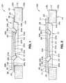
- FIG. 1illustrates a mounting 101 in accordance with one embodiment of the present invention.
- Mounting 101includes a semiconductor package 12 that is mounted on and electrically connected to an interconnective substrate 10 , which may be a motherboard or some other type of electronic chassis.
- Substrate 10includes a core layer 14 .
- layer 14may be a glass-fiber reinforced epoxy laminate sheet, a ceramic sheet, an insulated metal sheet, a film, or some other suitable material.
- Substrate 10includes a first surface 10 a and an opposite second surface 10 b .
- a rectangular aperture 10 cextends through substrate 10 between first surface 10 a and second surface 10 b .
- Conductive traces 20e.g., copper
- Traces 20carry electrical signals to and from package 12 .
- Semiconductor package 12includes a semiconductor chip 22 , a metal leadframe, and a body 24 of a hardened, insulative encapsulant material.
- the leadframeincludes a metal die pad 26 and horizontal metal leads 28 .
- Leads 28each include an inner lead portion 30 that is within body 24 , and an outer lead portion 32 that extends out of body 24 in the same horizontal plane as inner lead portion 30 and die pad 26 .
- the leadframemay be formed of copper, copper alloy, steel, Alloy 42 , or some other metal.
- Chip 22includes an active surface 22 a where integrated circuit devices are formed, and an opposite inactive surface 22 b .
- Active surface 22 aincludes a plurality of conductive bond pads 22 c along the edges of active surface 22 a .
- Bond pads 22 cmay be formed along two peripheral edges or all four peripheral edges of active surface 22 a .
- Inactive surface 22 b of chip 22may be polished to make chip 22 thinner, thereby reducing package height.
- Body 24has a planar first surface 24 a , an opposite planar second surface 24 b , and peripheral side surfaces 24 c .
- body 24may be formed by molding or pouring and then curing a resin material (e.g., epoxy resin). Where body 24 is molded, as in this example, side surfaces 24 c typically will be tapered to accommodate release from the mold.
- a resin materiale.g., epoxy resin
- Die pad 26has a planar first surface 26 a , an opposite second surface 26 b , and peripheral side surfaces 26 c .
- Inactive surface 22 b of chip 22is adhesively attached to first surface 26 a .
- Second surface 26 b of die pad 26is exposed in the plane of second surface 24 b of body 24 .
- First surface 26 a and side surfaces 26 c of die pad 26are covered by the encapsulant material of body 24 .
- die pad 26may be set up into body 24 , i.e., out of the horizontal plane of leads 28 and second surface 24 b of body 24 , so that second surface 26 b of die pad 26 is covered by the encapsulant material of body 24 .
- package 12has a reduced height, compared to the first conventional package mentioned above, because die pad 26 and leads 28 are provided at second surface 24 b of package body 24 .
- Package 12is electrically connected to traces 20 of second surface 10 b of substrate 10 so that electrical signals may be passed between substrate 10 and chip 22 of package 12 .
- each bond pad 22 c of chip 22is electrically connected by a conductor, e.g., a metal wire 34 made of gold or aluminum, to a first surface 28 a of an inner lead portion 30 of a lead 28 .
- Low loop bond wires or TAB bondsmay be used to help reduce package height.
- the first surface 28 a of each outer lead portion 30is electrically connected by a conductor, such as metal solder 36 , to metal traces 20 of substrate 10 .
- these electrical connectionsmay vary.
- a conductive adhesive materialsuch as a metal-filled epoxy, may be used instead of solder 36 to electrically connect outer leads 32 to metal traces 20 .
- Package 12is mounted on substrate 10 in a manner that significantly lessens a height of package 12 above second surface 10 b of substrate 10 , on which package 10 is mounted.
- package 12is mounted so that most of body 24 of package 12 is within aperture 10 c of substrate 10 .
- First surface 24 a of body 24 and a majority portion of side surfaces 24 c of body 24are within aperture 10 c .
- Only die pad 26 , leads 28 , and second surface 24 b of body 24are above second surface 10 b of substrate 10 , thereby accomplishing a very low mounting height.
- the height of package 10 of mounting 101 above second surface 10 b of substrateis about equal to the height (i.e., thickness) of die pad 26 and leads 28 .
- height savingsare realized by providing body 24 of package 10 within aperture 10 c , providing die pad 26 and leads 28 at second surface 24 b of body 24 rather than in the middle of body 24 , and, if desired, by thinning chip 22 and by using low-loop height bond wires 34 .
- FIG. 2depicts a mounting 102 in accordance with another embodiment of the present invention.
- Mounting 102is nearly the same as mounting 101 of FIG. 1, and thus does not need to be discussed in redundant detail.
- clips 11are provided on second surface 10 b of substrate 10 adjacent to aperture 10 c .
- Clips 11each include an electrically conductive portion that is electrically connected to one of the traces 20 of second surface 10 b .
- each clip 11may be metal, and may be soldered to one of the traces 20 .
- Outer leads 32 of package 12each snap into a respective one of the clips 11 , thereby electrically connecting package 12 to substrate 10 without a soldered or otherwise adhesive connection.
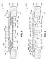
- FIG. 3depicts a mounting 103 in accordance with another embodiment of the present invention.
- the difference between mounting 103 of FIG. 3 and mounting 101 of FIG. 1is in the configuration of package 12 .
- inner lead portion 30 of each lead 28 of package 12 of FIG. 3is made longer, and the area of die pad 26 is reduced so as to fit within a boundary defined by bond pads 22 c .
- chip 22is mounted in a flip chip style on first surface 26 a of die pad 26 and first surface 28 a of the inner lead portions 30 .
- An insulative adhesiveis used to attach first surface 22 a of chip 22 to first surface 26 a of die pad 26 .
- FIG. 4depicts a mounting 104 in accordance with another embodiment of the present invention. Again, the difference between mounting 104 of FIG. 4 and mounting 101 of FIG. 1 is in the configuration of package 12 .
- Die pad 26 and leads 28 of package 12 of FIG. 4include a means for preventing die pad 26 and leads 28 from being pulled vertically from body 24 .
- this vertical locking featureincludes an undercut region 26 d at the periphery of die pad 26 that extends fully around, or extends at least along two opposing edges of, die pad 26 .
- this vertical locking featureincludes an undercut region 28 d in second surface 28 b of inner lead portion 30 .
- Encapsulant material of body 24fills in under undercut region 26 d of die pad 26 and undercut region 28 d of inner lead portion 30 .
- the underfilled encapsulant materialsupports die pad 26 and leads 28 in body 24 .
- Undercut regions 26 d and 28 dmay be formed by masking and then etching about half way through the thickness of die pad 26 and leads 28 in the regions shown.
- the readeris referred to U.S. patent application Ser. No. 09/176,614, which is incorporated herein by reference in its entirety.
- die pad 26 and leads 28may have a stamped or coined circumferential lip at first surface 26 a of die pad 26 and first surface 28 a of lead 28 .
- the lipcircumscribes die pad 26 , and extends along the side surfaces and inner end surface 28 c of each lead 28 .
- the lipultimately is underfilled by encapsulant material of body 24 , thereby vertically locking die pad 26 and leads 28 to body 24 .
- side surfaces 26 c of die pad 26 and the side surfaces and inner end surface 28 c of leads 28may include a central peak that extends into the encapsulant material or a central depression that is filled by the encapsulant material.
- U.S. Pat. No. 6,143,981which is incorporated herein by reference in its entirety.
- FIG. 7depicts a mounting 107 in accordance with another embodiment of the present invention. Again, the difference between mounting 107 of FIG. 7 and mounting 101 of FIG. 1 is in the configuration of the package.
- package 50includes a substrate 52 that includes a layer of insulative material 54 (e.g., a polyimide film, a glass-fiber reinforced laminate sheet, or ceramic) upon which metal circuit patterns 56 are formed.
- a body 24 of an insulative encapsulant materialis provided over a central region of a first surface 52 a of substrate 52 .
- a peripheral region of first surface 52 a around body 24is free of the encapsulant material.
- Body 24 of package 50is positioned in aperture 10 c of mounting substrate 10 , just as in FIG. 1 .
- the peripheral region of first surface 52 a of substrate 52is supported on first surface 10 a of substrate 10 around aperture 10 c .
- Outer end 56 b of each of the circuit patterns 56is connected by solder 36 or the like to one of the traces 20 on first surface 10 a of substrate 10 , thereby forming an electrical connection between package 50 and substrate 10 .
- package 50 of mounting 107has a very low height above second surface 10 b of substrate 10 .
- the height of package 50 of mounting 107is approximately equal to the thickness of substrate 52 of package 50 , since body 54 is in aperture 10 c.
- package 50may include further metal input/output terminals 58 on second surface 52 b of substrate 50 .
- Input/output terminals 58are electrically connected by vias 60 through substrate 50 to circuit patterns 56 on first surface 52 a . Accordingly, another package could be stacked on second surface 52 b if desired, and electrically connected to package 50 (and hence to substrate 10 ) through terminals 58 .
- FIG. 8depicts a mounting 108 in accordance with another embodiment of the present invention.
- the difference between mounting 108 of FIG. 8 and mounting 101 of FIG. 1is in the connection of package 12 to substrate 10 .
- substrate 10 of FIG. 8includes a plurality of metal-lined channels 10 d in second surface 10 b around aperture 10 c .
- the metal lining of each channel 10 dis electrically connected to a trace 20 of first surface 10 a .
- Channels 10 dare formed so that outer leads 32 of package 10 can be fitted or snapped therein, thereby forming a solderless electrical connection between package 12 and substrate 10 .
- soldermay be applied over leads 32 to make a more secure electrical connection to the metal lining of the respective channels 10 d . Accordingly, with body 24 in aperture 10 c and each outer lead 32 in a channel 10 d , second surface 24 b of body 24 of package 10 may be flush with or nearly flush with second surface 10 b of substrate 10 , depending on the depth of the channels 10 b.
- FIG. 9depicts a mounting 109 in accordance with another embodiment of the present invention.
- a second package 12is stacked on the package 12 of FIG. 1 that is mounted on substrate 10 .
- second surface 24 b of body 24 of the upper package 12is juxtaposed with and supported on the second surface 24 of body 24 of the lower package 12 .
- the exposed second surface 28 b of each lead 28 of the upper package 12is juxtaposed with and electrically connected by solder 36 or the like to the exposed second surface 28 b of one of the leads 28 of the lower package 12 , thereby electrically connecting the stacked packages 12 .
- the height of the stack of packages 12 above mounting surface 10 b of substrate 10is less than the sum of the heights of the two packages 12 unstacked. Further reductions in height may be obtained, for example, by using channels 10 d in substrate 10 , as shown in FIG. 8 .
- Mounting 109may be made by mounting a first package 12 on substrate 10 , as in FIG. 1, and then mounting a second package 12 on the first package 12 .
- the two packages 12can be electrically connected in a stack prior to electrically connecting the stack to substrate 10 .
- the two packagesmay include identical memory chips, with one package arranged to be the mirror image of the other so that the chips therein may be electrically connected in parallel.
Landscapes
- Engineering & Computer Science (AREA)
- Microelectronics & Electronic Packaging (AREA)
- Physics & Mathematics (AREA)
- Condensed Matter Physics & Semiconductors (AREA)
- General Physics & Mathematics (AREA)
- Computer Hardware Design (AREA)
- Power Engineering (AREA)
- Lead Frames For Integrated Circuits (AREA)
Abstract
Description
Claims (14)
Priority Applications (3)
| Application Number | Priority Date | Filing Date | Title |
|---|---|---|---|
| US09/813,485US6545345B1 (en) | 2001-03-20 | 2001-03-20 | Mounting for a package containing a chip |
| US10/340,256US6777789B1 (en) | 2001-03-20 | 2003-01-10 | Mounting for a package containing a chip |
| US10/688,138US6967395B1 (en) | 2001-03-20 | 2003-10-17 | Mounting for a package containing a chip |
Applications Claiming Priority (1)
| Application Number | Priority Date | Filing Date | Title |
|---|---|---|---|
| US09/813,485US6545345B1 (en) | 2001-03-20 | 2001-03-20 | Mounting for a package containing a chip |
Related Child Applications (1)
| Application Number | Title | Priority Date | Filing Date |
|---|---|---|---|
| US10/340,256ContinuationUS6777789B1 (en) | 2001-03-20 | 2003-01-10 | Mounting for a package containing a chip |
Publications (1)
| Publication Number | Publication Date |
|---|---|
| US6545345B1true US6545345B1 (en) | 2003-04-08 |
Family
ID=25212515
Family Applications (2)
| Application Number | Title | Priority Date | Filing Date |
|---|---|---|---|
| US09/813,485Expired - LifetimeUS6545345B1 (en) | 2001-03-20 | 2001-03-20 | Mounting for a package containing a chip |
| US10/340,256Expired - Fee RelatedUS6777789B1 (en) | 2001-03-20 | 2003-01-10 | Mounting for a package containing a chip |
Family Applications After (1)
| Application Number | Title | Priority Date | Filing Date |
|---|---|---|---|
| US10/340,256Expired - Fee RelatedUS6777789B1 (en) | 2001-03-20 | 2003-01-10 | Mounting for a package containing a chip |
Country Status (1)
| Country | Link |
|---|---|
| US (2) | US6545345B1 (en) |
Cited By (107)
| Publication number | Priority date | Publication date | Assignee | Title |
|---|---|---|---|---|
| US20030030152A1 (en)* | 2001-06-06 | 2003-02-13 | Corisis David J. | Thermally enhanced high density semiconductor package |
| US20040065905A1 (en)* | 2001-03-27 | 2004-04-08 | Jong Sik Paek | Semiconductor package and method for manufacturing the same |
| US6777789B1 (en)* | 2001-03-20 | 2004-08-17 | Amkor Technology, Inc. | Mounting for a package containing a chip |
| US6844615B1 (en) | 2003-03-13 | 2005-01-18 | Amkor Technology, Inc. | Leadframe package for semiconductor devices |
| US20050012207A1 (en)* | 2003-07-16 | 2005-01-20 | Jackson Hsieh | Substrate structure for an integrated circuit package and method for manufacturing the same |
| US6893900B1 (en) | 1998-06-24 | 2005-05-17 | Amkor Technology, Inc. | Method of making an integrated circuit package |
| US20050151229A1 (en)* | 2004-01-14 | 2005-07-14 | Denso Corporation | Electronic device having wiring substrate and lead frame |
| US6953988B2 (en) | 2000-03-25 | 2005-10-11 | Amkor Technology, Inc. | Semiconductor package |
| US6965157B1 (en) | 1999-11-09 | 2005-11-15 | Amkor Technology, Inc. | Semiconductor package with exposed die pad and body-locking leadframe |
| US6967395B1 (en) | 2001-03-20 | 2005-11-22 | Amkor Technology, Inc. | Mounting for a package containing a chip |
| US20050287703A1 (en)* | 2004-06-28 | 2005-12-29 | Semiconductor Components Industries, Llc. | Multi-chip semiconductor connector assembly method |
| US20060012002A1 (en)* | 2002-02-06 | 2006-01-19 | Remi Brechignac | Device for mounting a semiconductor package on a support plate via a base |
| US6995459B2 (en) | 2002-09-09 | 2006-02-07 | Amkor Technology, Inc. | Semiconductor package with increased number of input and output pins |
| US6998702B1 (en) | 2001-09-19 | 2006-02-14 | Amkor Technology, Inc. | Front edge chamfer feature for fully-molded memory cards |
| US7001799B1 (en) | 2003-03-13 | 2006-02-21 | Amkor Technology, Inc. | Method of making a leadframe for semiconductor devices |
| US7005326B1 (en) | 1998-06-24 | 2006-02-28 | Amkor Technology, Inc. | Method of making an integrated circuit package |
| US7030474B1 (en) | 1998-06-24 | 2006-04-18 | Amkor Technology, Inc. | Plastic integrated circuit package and method and leadframe for making the package |
| US7045883B1 (en) | 2001-04-04 | 2006-05-16 | Amkor Technology, Inc. | Thermally enhanced chip scale lead on chip semiconductor package and method of making same |
| US7045882B2 (en) | 2000-12-29 | 2006-05-16 | Amkor Technology, Inc. | Semiconductor package including flip chip |
| US7057280B2 (en) | 1998-11-20 | 2006-06-06 | Amkor Technology, Inc. | Leadframe having lead locks to secure leads to encapsulant |
| US7057268B1 (en) | 2004-01-27 | 2006-06-06 | Amkor Technology, Inc. | Cavity case with clip/plug for use on multi-media card |
| US7064009B1 (en) | 2001-04-04 | 2006-06-20 | Amkor Technology, Inc. | Thermally enhanced chip scale lead on chip semiconductor package and method of making same |
| US7067908B2 (en) | 1999-10-15 | 2006-06-27 | Amkor Technology, Inc. | Semiconductor package having improved adhesiveness and ground bonding |
| US7071541B1 (en) | 1998-06-24 | 2006-07-04 | Amkor Technology, Inc. | Plastic integrated circuit package and method and leadframe for making the package |
| US7091594B1 (en) | 2004-01-28 | 2006-08-15 | Amkor Technology, Inc. | Leadframe type semiconductor package having reduced inductance and its manufacturing method |
| US7102216B1 (en)* | 2001-08-17 | 2006-09-05 | Amkor Technology, Inc. | Semiconductor package and leadframe with horizontal leads spaced in the vertical direction and method of making |
| US20060208363A1 (en)* | 2005-03-16 | 2006-09-21 | Shiu Hei M | Three-dimensional package and method of forming same |
| US7112474B1 (en) | 1998-06-24 | 2006-09-26 | Amkor Technology, Inc. | Method of making an integrated circuit package |
| US7115445B2 (en) | 1999-10-15 | 2006-10-03 | Amkor Technology, Inc. | Semiconductor package having reduced thickness |
| US7138707B1 (en) | 2003-10-21 | 2006-11-21 | Amkor Technology, Inc. | Semiconductor package including leads and conductive posts for providing increased functionality |
| US7144517B1 (en) | 2003-11-07 | 2006-12-05 | Amkor Technology, Inc. | Manufacturing method for leadframe and for semiconductor package using the leadframe |
| US7160798B2 (en) | 2005-02-24 | 2007-01-09 | Freescale Semiconductor, Inc. | Method of making reinforced semiconductor package |
| US7170150B2 (en) | 2001-03-27 | 2007-01-30 | Amkor Technology, Inc. | Lead frame for semiconductor package |
| US7190062B1 (en) | 2004-06-15 | 2007-03-13 | Amkor Technology, Inc. | Embedded leadframe semiconductor package |
| US7192807B1 (en) | 2002-11-08 | 2007-03-20 | Amkor Technology, Inc. | Wafer level package and fabrication method |
| US7202554B1 (en) | 2004-08-19 | 2007-04-10 | Amkor Technology, Inc. | Semiconductor package and its manufacturing method |
| US7211879B1 (en) | 2003-11-12 | 2007-05-01 | Amkor Technology, Inc. | Semiconductor package with chamfered corners and method of manufacturing the same |
| US7217991B1 (en) | 2004-10-22 | 2007-05-15 | Amkor Technology, Inc. | Fan-in leadframe semiconductor package |
| US7253503B1 (en) | 1999-11-05 | 2007-08-07 | Amkor Technology, Inc. | Integrated circuit device packages and substrates for making the packages |
| US7332375B1 (en) | 1998-06-24 | 2008-02-19 | Amkor Technology, Inc. | Method of making an integrated circuit package |
| US7361533B1 (en) | 2002-11-08 | 2008-04-22 | Amkor Technology, Inc. | Stacked embedded leadframe |
| US7381588B1 (en)* | 2002-12-20 | 2008-06-03 | Asat Ltd. | Shielded integrated circuit package |
| US7411289B1 (en)* | 2004-06-14 | 2008-08-12 | Asat Ltd. | Integrated circuit package with partially exposed contact pads and process for fabricating the same |
| US7507603B1 (en) | 2005-12-02 | 2009-03-24 | Amkor Technology, Inc. | Etch singulated semiconductor package |
| US7531383B2 (en) | 2006-10-31 | 2009-05-12 | Freescale Semiconductor, Inc. | Array quad flat no-lead package and method of forming same |
| US7572681B1 (en) | 2005-12-08 | 2009-08-11 | Amkor Technology, Inc. | Embedded electronic component package |
| US7598598B1 (en) | 2003-02-05 | 2009-10-06 | Amkor Technology, Inc. | Offset etched corner leads for semiconductor package |
| US7687899B1 (en) | 2007-08-07 | 2010-03-30 | Amkor Technology, Inc. | Dual laminate package structure with embedded elements |
| US7687893B2 (en) | 2006-12-27 | 2010-03-30 | Amkor Technology, Inc. | Semiconductor package having leadframe with exposed anchor pads |
| US7723210B2 (en) | 2002-11-08 | 2010-05-25 | Amkor Technology, Inc. | Direct-write wafer level chip scale package |
| US7723852B1 (en) | 2008-01-21 | 2010-05-25 | Amkor Technology, Inc. | Stacked semiconductor package and method of making same |
| US20100177490A1 (en)* | 2009-01-14 | 2010-07-15 | Micron Technology, Inc. | Computer modules with small thicknesses and associated methods of manufacturing |
| US7768135B1 (en) | 2008-04-17 | 2010-08-03 | Amkor Technology, Inc. | Semiconductor package with fast power-up cycle and method of making same |
| US7777351B1 (en) | 2007-10-01 | 2010-08-17 | Amkor Technology, Inc. | Thin stacked interposer package |
| US7808084B1 (en) | 2008-05-06 | 2010-10-05 | Amkor Technology, Inc. | Semiconductor package with half-etched locking features |
| US7829990B1 (en) | 2007-01-18 | 2010-11-09 | Amkor Technology, Inc. | Stackable semiconductor package including laminate interposer |
| US7847392B1 (en) | 2008-09-30 | 2010-12-07 | Amkor Technology, Inc. | Semiconductor device including leadframe with increased I/O |
| US7847386B1 (en) | 2007-11-05 | 2010-12-07 | Amkor Technology, Inc. | Reduced size stacked semiconductor package and method of making the same |
| US7875963B1 (en) | 2008-11-21 | 2011-01-25 | Amkor Technology, Inc. | Semiconductor device including leadframe having power bars and increased I/O |
| US7902660B1 (en) | 2006-05-24 | 2011-03-08 | Amkor Technology, Inc. | Substrate for semiconductor device and manufacturing method thereof |
| US7956453B1 (en) | 2008-01-16 | 2011-06-07 | Amkor Technology, Inc. | Semiconductor package with patterning layer and method of making same |
| US7960818B1 (en) | 2009-03-04 | 2011-06-14 | Amkor Technology, Inc. | Conformal shield on punch QFN semiconductor package |
| US7968998B1 (en) | 2006-06-21 | 2011-06-28 | Amkor Technology, Inc. | Side leaded, bottom exposed pad and bottom exposed lead fusion quad flat semiconductor package |
| US7977774B2 (en) | 2007-07-10 | 2011-07-12 | Amkor Technology, Inc. | Fusion quad flat semiconductor package |
| US7982298B1 (en) | 2008-12-03 | 2011-07-19 | Amkor Technology, Inc. | Package in package semiconductor device |
| US7982297B1 (en) | 2007-03-06 | 2011-07-19 | Amkor Technology, Inc. | Stackable semiconductor package having partially exposed semiconductor die and method of fabricating the same |
| US7989933B1 (en) | 2008-10-06 | 2011-08-02 | Amkor Technology, Inc. | Increased I/O leadframe and semiconductor device including same |
| US8008758B1 (en) | 2008-10-27 | 2011-08-30 | Amkor Technology, Inc. | Semiconductor device with increased I/O leadframe |
| US8026589B1 (en) | 2009-02-23 | 2011-09-27 | Amkor Technology, Inc. | Reduced profile stackable semiconductor package |
| US8058715B1 (en) | 2009-01-09 | 2011-11-15 | Amkor Technology, Inc. | Package in package device for RF transceiver module |
| US8067821B1 (en) | 2008-04-10 | 2011-11-29 | Amkor Technology, Inc. | Flat semiconductor package with half package molding |
| US8072050B1 (en) | 2008-11-18 | 2011-12-06 | Amkor Technology, Inc. | Semiconductor device with increased I/O leadframe including passive device |
| US8089145B1 (en) | 2008-11-17 | 2012-01-03 | Amkor Technology, Inc. | Semiconductor device including increased capacity leadframe |
| US8089159B1 (en) | 2007-10-03 | 2012-01-03 | Amkor Technology, Inc. | Semiconductor package with increased I/O density and method of making the same |
| US8125064B1 (en) | 2008-07-28 | 2012-02-28 | Amkor Technology, Inc. | Increased I/O semiconductor package and method of making same |
| US8184453B1 (en) | 2008-07-31 | 2012-05-22 | Amkor Technology, Inc. | Increased capacity semiconductor package |
| US8294276B1 (en) | 2010-05-27 | 2012-10-23 | Amkor Technology, Inc. | Semiconductor device and fabricating method thereof |
| US8318287B1 (en) | 1998-06-24 | 2012-11-27 | Amkor Technology, Inc. | Integrated circuit package and method of making the same |
| US8324511B1 (en) | 2010-04-06 | 2012-12-04 | Amkor Technology, Inc. | Through via nub reveal method and structure |
| US8390130B1 (en) | 2011-01-06 | 2013-03-05 | Amkor Technology, Inc. | Through via recessed reveal structure and method |
| US8410585B2 (en) | 2000-04-27 | 2013-04-02 | Amkor Technology, Inc. | Leadframe and semiconductor package made using the leadframe |
| US8440554B1 (en) | 2010-08-02 | 2013-05-14 | Amkor Technology, Inc. | Through via connected backside embedded circuit features structure and method |
| US8487420B1 (en) | 2008-12-08 | 2013-07-16 | Amkor Technology, Inc. | Package in package semiconductor device with film over wire |
| US8487445B1 (en) | 2010-10-05 | 2013-07-16 | Amkor Technology, Inc. | Semiconductor device having through electrodes protruding from dielectric layer |
| US8552548B1 (en) | 2011-11-29 | 2013-10-08 | Amkor Technology, Inc. | Conductive pad on protruding through electrode semiconductor device |
| US8575742B1 (en) | 2009-04-06 | 2013-11-05 | Amkor Technology, Inc. | Semiconductor device with increased I/O leadframe including power bars |
| US8588017B2 (en) | 2010-10-20 | 2013-11-19 | Samsung Electronics Co., Ltd. | Memory circuits, systems, and modules for performing DRAM refresh operations and methods of operating the same |
| US8648450B1 (en) | 2011-01-27 | 2014-02-11 | Amkor Technology, Inc. | Semiconductor device including leadframe with a combination of leads and lands |
| US8674485B1 (en) | 2010-12-08 | 2014-03-18 | Amkor Technology, Inc. | Semiconductor device including leadframe with downsets |
| US8680656B1 (en) | 2009-01-05 | 2014-03-25 | Amkor Technology, Inc. | Leadframe structure for concentrated photovoltaic receiver package |
| US8791501B1 (en) | 2010-12-03 | 2014-07-29 | Amkor Technology, Inc. | Integrated passive device structure and method |
| US8796561B1 (en) | 2009-10-05 | 2014-08-05 | Amkor Technology, Inc. | Fan out build up substrate stackable package and method |
| US8937381B1 (en) | 2009-12-03 | 2015-01-20 | Amkor Technology, Inc. | Thin stackable package and method |
| US9048298B1 (en) | 2012-03-29 | 2015-06-02 | Amkor Technology, Inc. | Backside warpage control structure and fabrication method |
| US9129943B1 (en) | 2012-03-29 | 2015-09-08 | Amkor Technology, Inc. | Embedded component package and fabrication method |
| US9184118B2 (en) | 2013-05-02 | 2015-11-10 | Amkor Technology Inc. | Micro lead frame structure having reinforcing portions and method |
| US9184148B2 (en) | 2013-10-24 | 2015-11-10 | Amkor Technology, Inc. | Semiconductor package and method therefor |
| US9631481B1 (en) | 2011-01-27 | 2017-04-25 | Amkor Technology, Inc. | Semiconductor device including leadframe with a combination of leads and lands and method |
| US9673122B2 (en) | 2014-05-02 | 2017-06-06 | Amkor Technology, Inc. | Micro lead frame structure having reinforcing portions and method |
| US9691734B1 (en) | 2009-12-07 | 2017-06-27 | Amkor Technology, Inc. | Method of forming a plurality of electronic component packages |
| US9704725B1 (en) | 2012-03-06 | 2017-07-11 | Amkor Technology, Inc. | Semiconductor device with leadframe configured to facilitate reduced burr formation |
| US20180166413A1 (en)* | 2016-12-09 | 2018-06-14 | Fraunhofer-Gesellschaft Zur Foerderung Der Angewandten Forschung E.V. | Electrically conductive bond between at least two electrical components at a carrier mounted with electronic and/or electrical devices, said bond being formed by a bond wire |
| US10373895B2 (en)* | 2016-12-12 | 2019-08-06 | Infineon Technologies Austria Ag | Semiconductor device having die pads with exposed surfaces |
| US10811341B2 (en) | 2009-01-05 | 2020-10-20 | Amkor Technology Singapore Holding Pte Ltd. | Semiconductor device with through-mold via |
| US20220084915A1 (en)* | 2020-09-16 | 2022-03-17 | Infineon Technologies Austria Ag | Semiconductor Package, Semiconductor Module and Methods for Manufacturing a Semiconductor Package and a Semiconductor Module |
| US20240128240A1 (en)* | 2019-08-02 | 2024-04-18 | Semiconductor Components Industries, Llc | Low stress asymmetric dual side module |
| US20240203846A1 (en)* | 2019-08-02 | 2024-06-20 | Semiconductor Components Industries, Llc | Low stress asymmetric dual side module |
Families Citing this family (16)
| Publication number | Priority date | Publication date | Assignee | Title |
|---|---|---|---|---|
| US7132311B2 (en)* | 2002-07-26 | 2006-11-07 | Intel Corporation | Encapsulation of a stack of semiconductor dice |
| JP4372508B2 (en)* | 2003-10-06 | 2009-11-25 | ローム株式会社 | Lead frame manufacturing method, semiconductor device manufacturing method using the same, semiconductor device, and portable device and electronic device including the same |
| US20070108635A1 (en)* | 2005-04-28 | 2007-05-17 | Stats Chippac Ltd. | Integrated circuit package system |
| US20070132075A1 (en)* | 2005-12-12 | 2007-06-14 | Mutsumi Masumoto | Structure and method for thin single or multichip semiconductor QFN packages |
| US7777354B2 (en)* | 2007-06-05 | 2010-08-17 | Stats Chippac Ltd. | Integrated circuit package system with leaded package |
| US8115285B2 (en)* | 2008-03-14 | 2012-02-14 | Advanced Semiconductor Engineering, Inc. | Advanced quad flat no lead chip package having a protective layer to enhance surface mounting and manufacturing methods thereof |
| US7875965B2 (en)* | 2008-03-18 | 2011-01-25 | Mediatek Inc. | Semiconductor chip package |
| US20100044850A1 (en)* | 2008-08-21 | 2010-02-25 | Advanced Semiconductor Engineering, Inc. | Advanced quad flat non-leaded package structure and manufacturing method thereof |
| JP5242644B2 (en)* | 2010-08-31 | 2013-07-24 | 株式会社東芝 | Semiconductor memory device |
| US20120139095A1 (en)* | 2010-12-03 | 2012-06-07 | Manusharow Mathew J | Low-profile microelectronic package, method of manufacturing same, and electronic assembly containing same |
| US9209121B2 (en)* | 2013-02-01 | 2015-12-08 | Analog Devices, Inc. | Double-sided package |
| US9731959B2 (en) | 2014-09-25 | 2017-08-15 | Analog Devices, Inc. | Integrated device packages having a MEMS die sealed in a cavity by a processor die and method of manufacturing the same |
| US9533878B2 (en) | 2014-12-11 | 2017-01-03 | Analog Devices, Inc. | Low stress compact device packages |
| US11302611B2 (en)* | 2018-11-28 | 2022-04-12 | Texas Instruments Incorporated | Semiconductor package with top circuit and an IC with a gap over the IC |
| US11296005B2 (en) | 2019-09-24 | 2022-04-05 | Analog Devices, Inc. | Integrated device package including thermally conductive element and method of manufacturing same |
| US12315776B2 (en) | 2021-11-08 | 2025-05-27 | Analog Devices, Inc. | Integrated device package with an integrated heat sink |
Citations (3)
| Publication number | Priority date | Publication date | Assignee | Title |
|---|---|---|---|---|
| US5894108A (en)* | 1997-02-11 | 1999-04-13 | National Semiconductor Corporation | Plastic package with exposed die |
| US6326244B1 (en)* | 1998-09-03 | 2001-12-04 | Micron Technology, Inc. | Method of making a cavity ball grid array apparatus |
| US6380048B1 (en)* | 2001-08-02 | 2002-04-30 | St Assembly Test Services Pte Ltd | Die paddle enhancement for exposed pad in semiconductor packaging |
Family Cites Families (220)
| Publication number | Priority date | Publication date | Assignee | Title |
|---|---|---|---|---|
| US2596993A (en) | 1949-01-13 | 1952-05-20 | United Shoe Machinery Corp | Method and mold for covering of eyelets by plastic injection |
| US3734660A (en) | 1970-01-09 | 1973-05-22 | Tuthill Pump Co | Apparatus for fabricating a bearing device |
| US4189342A (en) | 1971-10-07 | 1980-02-19 | U.S. Philips Corporation | Semiconductor device comprising projecting contact layers |
| US3838984A (en) | 1973-04-16 | 1974-10-01 | Sperry Rand Corp | Flexible carrier and interconnect for uncased ic chips |
| US4054238A (en) | 1976-03-23 | 1977-10-18 | Western Electric Company, Inc. | Method, apparatus and lead frame for assembling leads with terminals on a substrate |
| JPS5479563A (en) | 1977-12-07 | 1979-06-25 | Kyushu Nippon Electric | Lead frame for semiconductor |
| US4332537A (en) | 1978-07-17 | 1982-06-01 | Dusan Slepcevic | Encapsulation mold with removable cavity plates |
| JPS5521128A (en) | 1978-08-02 | 1980-02-15 | Hitachi Ltd | Lead frame used for semiconductor device and its assembling |
| US4289922A (en) | 1979-09-04 | 1981-09-15 | Plessey Incorporated | Integrated circuit package and lead frame |
| US4417266A (en) | 1981-08-14 | 1983-11-22 | Amp Incorporated | Power and ground plane structure for chip carrier |
| US4451224A (en) | 1982-03-25 | 1984-05-29 | General Electric Company | Mold device for making plastic articles from resin |
| FR2524707B1 (en) | 1982-04-01 | 1985-05-31 | Cit Alcatel | METHOD OF ENCAPSULATION OF SEMICONDUCTOR COMPONENTS, AND ENCAPSULATED COMPONENTS OBTAINED |
| US4737839A (en) | 1984-03-19 | 1988-04-12 | Trilogy Computer Development Partners, Ltd. | Semiconductor chip mounting system |
| JPH0612796B2 (en) | 1984-06-04 | 1994-02-16 | 株式会社日立製作所 | Semiconductor device |
| US4862246A (en) | 1984-09-26 | 1989-08-29 | Hitachi, Ltd. | Semiconductor device lead frame with etched through holes |
| US4862245A (en) | 1985-04-18 | 1989-08-29 | International Business Machines Corporation | Package semiconductor chip |
| US4756080A (en) | 1986-01-27 | 1988-07-12 | American Microsystems, Inc. | Metal foil semiconductor interconnection method |
| US4812896A (en) | 1986-11-13 | 1989-03-14 | Olin Corporation | Metal electronic package sealed with thermoplastic having a grafted metal deactivator and antioxidant |
| US5087961A (en) | 1987-01-28 | 1992-02-11 | Lsi Logic Corporation | Semiconductor device package |
| KR960006710B1 (en) | 1987-02-25 | 1996-05-22 | 가부시기가이샤 히다찌세이사꾸쇼 | Surface mount plastic package semiconductor integrated circuit and the manufacturing method thereof and well asmount struct |
| US5059379A (en) | 1987-07-20 | 1991-10-22 | Mitsubishi Denki Kabushiki Kaisha | Method of resin sealing semiconductor devices |
| US4942454A (en) | 1987-08-05 | 1990-07-17 | Mitsubishi Denki Kabushiki Kaisha | Resin sealed semiconductor device |
| US4987475A (en) | 1988-02-29 | 1991-01-22 | Digital Equipment Corporation | Alignment of leads for ceramic integrated circuit packages |
| US4907067A (en) | 1988-05-11 | 1990-03-06 | Texas Instruments Incorporated | Thermally efficient power device package |
| US5096852A (en) | 1988-06-02 | 1992-03-17 | Burr-Brown Corporation | Method of making plastic encapsulated multichip hybrid integrated circuits |
| US4935803A (en) | 1988-09-09 | 1990-06-19 | Motorola, Inc. | Self-centering electrode for power devices |
| DE68922812T2 (en) | 1988-09-29 | 1995-12-07 | Tomoegawa Paper Mfg Co Ltd | Adhesive tapes. |
| US5277972B1 (en) | 1988-09-29 | 1996-11-05 | Tomoegawa Paper Co Ltd | Adhesive tapes |
| US5266834A (en) | 1989-03-13 | 1993-11-30 | Hitachi Ltd. | Semiconductor device and an electronic device with the semiconductor devices mounted thereon |
| US5070039A (en) | 1989-04-13 | 1991-12-03 | Texas Instruments Incorporated | Method of making an integrated circuit using a pre-served dam bar to reduce mold flash and to facilitate flash removal |
| JPH02306639A (en) | 1989-05-22 | 1990-12-20 | Toshiba Corp | Resin encapsulating method for semiconductor device |
| EP0405755B1 (en) | 1989-05-31 | 1995-11-29 | Fujitsu Limited | Pin grid array packaging structure |
| JPH0671062B2 (en) | 1989-08-30 | 1994-09-07 | 株式会社東芝 | Resin-sealed semiconductor device |
| US5200362A (en) | 1989-09-06 | 1993-04-06 | Motorola, Inc. | Method of attaching conductive traces to an encapsulated semiconductor die using a removable transfer film |
| US5041902A (en) | 1989-12-14 | 1991-08-20 | Motorola, Inc. | Molded electronic package with compression structures |
| CA2047486C (en) | 1990-07-21 | 2002-03-05 | Shigeru Katayama | Semiconductor device and method for manufacturing the same |
| EP0509065A1 (en) | 1990-08-01 | 1992-10-21 | Staktek Corporation | Ultra high density integrated circuit packages, method and apparatus |
| US5029386A (en) | 1990-09-17 | 1991-07-09 | Hewlett-Packard Company | Hierarchical tape automated bonding method |
| US5335771A (en) | 1990-09-25 | 1994-08-09 | R. H. Murphy Company, Inc. | Spacer trays for stacking storage trays with integrated circuits |
| US5391439A (en) | 1990-09-27 | 1995-02-21 | Dai Nippon Printing Co., Ltd. | Leadframe adapted to support semiconductor elements |
| US5298685A (en) | 1990-10-30 | 1994-03-29 | International Business Machines Corporation | Interconnection method and structure for organic circuit boards |
| US5216278A (en) | 1990-12-04 | 1993-06-01 | Motorola, Inc. | Semiconductor device having a pad array carrier package |
| US5157480A (en) | 1991-02-06 | 1992-10-20 | Motorola, Inc. | Semiconductor device having dual electrical contact sites |
| US5172214A (en) | 1991-02-06 | 1992-12-15 | Motorola, Inc. | Leadless semiconductor device and method for making the same |
| US5281849A (en)* | 1991-05-07 | 1994-01-25 | Singh Deo Narendra N | Semiconductor package with segmented lead frame |
| US5172213A (en) | 1991-05-23 | 1992-12-15 | At&T Bell Laboratories | Molded circuit package having heat dissipating post |
| US5221642A (en) | 1991-08-15 | 1993-06-22 | Staktek Corporation | Lead-on-chip integrated circuit fabrication method |
| JP2658661B2 (en) | 1991-09-18 | 1997-09-30 | 日本電気株式会社 | Method for manufacturing multilayer printed wiring board |
| JP2518569B2 (en) | 1991-09-19 | 1996-07-24 | 三菱電機株式会社 | Semiconductor device |
| US5200809A (en) | 1991-09-27 | 1993-04-06 | Vlsi Technology, Inc. | Exposed die-attach heatsink package |
| US5332864A (en) | 1991-12-27 | 1994-07-26 | Vlsi Technology, Inc. | Integrated circuit package having an interposer |
| JPH06120374A (en) | 1992-03-31 | 1994-04-28 | Amkor Electron Inc | Semiconductor package structure, semicon- ductor packaging method and heat sink for semiconductor package |
| US5250841A (en) | 1992-04-06 | 1993-10-05 | Motorola, Inc. | Semiconductor device with test-only leads |
| US5539251A (en) | 1992-05-11 | 1996-07-23 | Micron Technology, Inc. | Tie bar over chip lead frame design |
| US5214845A (en) | 1992-05-11 | 1993-06-01 | Micron Technology, Inc. | Method for producing high speed integrated circuits |
| KR100260347B1 (en) | 1992-06-05 | 2000-07-01 | 나까니시 히로유끼 | 3D printed board, electronic circuit package and printed board manufacturing method using the same |
| US5278446A (en) | 1992-07-06 | 1994-01-11 | Motorola, Inc. | Reduced stress plastic package |
| JPH0637202A (en) | 1992-07-20 | 1994-02-10 | Mitsubishi Electric Corp | Microwave IC package |
| JPH0653394A (en) | 1992-07-28 | 1994-02-25 | Shinko Electric Ind Co Ltd | Plane support for multilayer lead frame |
| US5592025A (en) | 1992-08-06 | 1997-01-07 | Motorola, Inc. | Pad array semiconductor device |
| KR0128251Y1 (en) | 1992-08-21 | 1998-10-15 | 문정환 | Lead exposed type semiconductor device |
| US5608267A (en) | 1992-09-17 | 1997-03-04 | Olin Corporation | Molded plastic semiconductor package including heat spreader |
| US5859471A (en) | 1992-11-17 | 1999-01-12 | Shinko Electric Industries Co., Ltd. | Semiconductor device having tab tape lead frame with reinforced outer leads |
| US5409362A (en) | 1992-11-24 | 1995-04-25 | Neu Dynamics Corp. | Encapsulation molding equipment |
| US5406124A (en) | 1992-12-04 | 1995-04-11 | Mitsui Toatsu Chemicals, Inc. | Insulating adhesive tape, and lead frame and semiconductor device employing the tape |
| US5457340A (en) | 1992-12-07 | 1995-10-10 | Integrated Device Technology, Inc. | Leadframe with power and ground planes |
| KR960009089B1 (en) | 1993-03-04 | 1996-07-10 | 문정환 | Mold for package molding and plastic charge-coupled device and the manufacturing method using the mold |
| US5340771A (en) | 1993-03-18 | 1994-08-23 | Lsi Logic Corporation | Techniques for providing high I/O count connections to semiconductor dies |
| US5327008A (en) | 1993-03-22 | 1994-07-05 | Motorola Inc. | Semiconductor device having universal low-stress die support and method for making the same |
| US5291061A (en) | 1993-04-06 | 1994-03-01 | Micron Semiconductor, Inc. | Multi-chip stacked devices |
| US5474958A (en) | 1993-05-04 | 1995-12-12 | Motorola, Inc. | Method for making semiconductor device having no die supporting surface |
| KR0152901B1 (en) | 1993-06-23 | 1998-10-01 | 문정환 | Plastic package and method for manufacture thereof |
| JP2526787B2 (en) | 1993-07-01 | 1996-08-21 | 日本電気株式会社 | Lead frame for semiconductor device |
| JP2875139B2 (en) | 1993-07-15 | 1999-03-24 | 株式会社東芝 | Method for manufacturing semiconductor device |
| US5336931A (en) | 1993-09-03 | 1994-08-09 | Motorola, Inc. | Anchoring method for flow formed integrated circuit covers |
| US5641997A (en) | 1993-09-14 | 1997-06-24 | Kabushiki Kaisha Toshiba | Plastic-encapsulated semiconductor device |
| US5414299A (en) | 1993-09-24 | 1995-05-09 | Vlsi Technology, Inc. | Semi-conductor device interconnect package assembly for improved package performance |
| US5517056A (en) | 1993-09-30 | 1996-05-14 | Motorola, Inc. | Molded carrier ring leadframe having a particular resin injecting area design for gate removal and semiconductor device employing the same |
| US5545923A (en) | 1993-10-22 | 1996-08-13 | Lsi Logic Corporation | Semiconductor device assembly with minimized bond finger connections |
| JPH07142627A (en) | 1993-11-18 | 1995-06-02 | Fujitsu Ltd | Semiconductor device and manufacturing method thereof |
| US5521429A (en) | 1993-11-25 | 1996-05-28 | Sanyo Electric Co., Ltd. | Surface-mount flat package semiconductor device |
| US5673479A (en) | 1993-12-20 | 1997-10-07 | Lsi Logic Corporation | Method for mounting a microelectronic circuit peripherally-leaded package including integral support member with spacer |
| US5821457A (en) | 1994-03-11 | 1998-10-13 | The Panda Project | Semiconductor die carrier having a dielectric epoxy between adjacent leads |
| JP3247384B2 (en) | 1994-03-18 | 2002-01-15 | 日立化成工業株式会社 | Semiconductor package manufacturing method and semiconductor package |
| KR970010676B1 (en) | 1994-03-29 | 1997-06-30 | 엘지반도체 주식회사 | Semiconductor package and lead frame used therein |
| JPH07288309A (en) | 1994-04-19 | 1995-10-31 | Mitsubishi Electric Corp | Semiconductor device, manufacturing method thereof, and semiconductor module |
| US5701034A (en) | 1994-05-03 | 1997-12-23 | Amkor Electronics, Inc. | Packaged semiconductor die including heat sink with locking feature |
| US5544412A (en) | 1994-05-24 | 1996-08-13 | Motorola, Inc. | Method for coupling a power lead to a bond pad in an electronic module |
| US5429992A (en) | 1994-05-25 | 1995-07-04 | Texas Instruments Incorporated | Lead frame structure for IC devices with strengthened encapsulation adhesion |
| US5766972A (en) | 1994-06-02 | 1998-06-16 | Mitsubishi Denki Kabushiki Kaisha | Method of making resin encapsulated semiconductor device with bump electrodes |
| US5604376A (en) | 1994-06-30 | 1997-02-18 | Digital Equipment Corporation | Paddleless molded plastic semiconductor chip package |
| JPH0837252A (en) | 1994-07-22 | 1996-02-06 | Nec Corp | Semiconductor device |
| US5454905A (en) | 1994-08-09 | 1995-10-03 | National Semiconductor Corporation | Method for manufacturing fine pitch lead frame |
| KR0145768B1 (en) | 1994-08-16 | 1998-08-01 | 김광호 | Lead frame and manufacturing method of semiconductor package using same |
| JP2820645B2 (en) | 1994-08-30 | 1998-11-05 | アナム インダストリアル カンパニー インコーポレーティド | Semiconductor lead frame |
| US5508556A (en) | 1994-09-02 | 1996-04-16 | Motorola, Inc. | Leaded semiconductor device having accessible power supply pad terminals |
| US5543657A (en) | 1994-10-07 | 1996-08-06 | International Business Machines Corporation | Single layer leadframe design with groundplane capability |
| US5581122A (en) | 1994-10-25 | 1996-12-03 | Industrial Technology Research Institute | Packaging assembly with consolidated common voltage connections for integrated circuits |
| US5665996A (en) | 1994-12-30 | 1997-09-09 | Siliconix Incorporated | Vertical power mosfet having thick metal layer to reduce distributed resistance |
| US5767546A (en) | 1994-12-30 | 1998-06-16 | Siliconix Incorporated | Laternal power mosfet having metal strap layer to reduce distributed resistance |
| JPH08222681A (en) | 1995-02-14 | 1996-08-30 | Toshiba Corp | Resin-sealed semiconductor device |
| JPH08306853A (en) | 1995-05-09 | 1996-11-22 | Fujitsu Ltd | Semiconductor device, method of manufacturing the same, and method of manufacturing lead frame |
| US6323550B1 (en) | 1995-06-06 | 2001-11-27 | Analog Devices, Inc. | Package for sealing an integrated circuit die |
| KR100214463B1 (en) | 1995-12-06 | 1999-08-02 | 구본준 | Lead frame of clip type and method manufacture of the package |
| US5650663A (en) | 1995-07-03 | 1997-07-22 | Olin Corporation | Electronic package with improved thermal properties |
| US5745984A (en) | 1995-07-10 | 1998-05-05 | Martin Marietta Corporation | Method for making an electronic module |
| JP3170182B2 (en) | 1995-08-15 | 2001-05-28 | 株式会社東芝 | Resin-sealed semiconductor device and method of manufacturing the same |
| US6239384B1 (en) | 1995-09-18 | 2001-05-29 | Tessera, Inc. | Microelectric lead structures with plural conductors |
| JP3123638B2 (en) | 1995-09-25 | 2001-01-15 | 株式会社三井ハイテック | Semiconductor device |
| JPH0992776A (en) | 1995-09-28 | 1997-04-04 | Mitsubishi Electric Corp | Lead frame and semiconductor device |
| JP3292798B2 (en) | 1995-10-04 | 2002-06-17 | 三菱電機株式会社 | Semiconductor device |
| US5801440A (en) | 1995-10-10 | 1998-09-01 | Acc Microelectronics Corporation | Chip package board having utility rings |
| US5696666A (en) | 1995-10-11 | 1997-12-09 | Motorola, Inc. | Low profile exposed die chip carrier package |
| JP3176542B2 (en) | 1995-10-25 | 2001-06-18 | シャープ株式会社 | Semiconductor device and manufacturing method thereof |
| KR0163871B1 (en) | 1995-11-25 | 1998-12-01 | 김광호 | Solder Ball Array Package with Heat Sink Attached to Bottom |
| KR0167297B1 (en) | 1995-12-18 | 1998-12-15 | 문정환 | L.O.C package and its manufacturing method |
| US5689135A (en) | 1995-12-19 | 1997-11-18 | Micron Technology, Inc. | Multi-chip device and method of fabrication employing leads over and under processes |
| US5646831A (en) | 1995-12-28 | 1997-07-08 | Vlsi Technology, Inc. | Electrically enhanced power quad flat pack arrangement |
| KR0179803B1 (en) | 1995-12-29 | 1999-03-20 | 문정환 | Lead Exposure Semiconductor Package |
| KR0157929B1 (en) | 1995-12-30 | 1999-01-15 | 문정환 | Semiconductor package molding apparatus of multi-layer mold type |
| US5866939A (en) | 1996-01-21 | 1999-02-02 | Anam Semiconductor Inc. | Lead end grid array semiconductor package |
| US5760465A (en) | 1996-02-01 | 1998-06-02 | International Business Machines Corporation | Electronic package with strain relief means |
| US5977613A (en) | 1996-03-07 | 1999-11-02 | Matsushita Electronics Corporation | Electronic component, method for making the same, and lead frame and mold assembly for use therein |
| JPH09260575A (en) | 1996-03-22 | 1997-10-03 | Mitsubishi Electric Corp | Semiconductor device and lead frame |
| JPH09260538A (en) | 1996-03-27 | 1997-10-03 | Miyazaki Oki Electric Co Ltd | Resin sealed semiconductor device manufacturing method and its mounting structure |
| JPH09260568A (en) | 1996-03-27 | 1997-10-03 | Mitsubishi Electric Corp | Semiconductor device and manufacturing method thereof |
| US6169329B1 (en) | 1996-04-02 | 2001-01-02 | Micron Technology, Inc. | Semiconductor devices having interconnections using standardized bonding locations and methods of designing |
| US6001671A (en) | 1996-04-18 | 1999-12-14 | Tessera, Inc. | Methods for manufacturing a semiconductor package having a sacrificial layer |
| KR100186309B1 (en) | 1996-05-17 | 1999-03-20 | 문정환 | Stacked bottom lead package |
| US5917242A (en) | 1996-05-20 | 1999-06-29 | Micron Technology, Inc. | Combination of semiconductor interconnect |
| JP3469038B2 (en) | 1996-06-10 | 2003-11-25 | ローレルバンクマシン株式会社 | Bill validator |
| DE69735361T2 (en) | 1996-07-03 | 2006-10-19 | Seiko Epson Corp. | Resin-encapsulated semi-conductor arrangement and method of production therefor |
| KR0185512B1 (en) | 1996-08-19 | 1999-03-20 | 김광호 | Column lead type package and method of making the same |
| DE19635582C1 (en) | 1996-09-02 | 1998-02-19 | Siemens Ag | Power semiconductor component for bridge circuits with high or low side switches |
| US5776798A (en) | 1996-09-04 | 1998-07-07 | Motorola, Inc. | Semiconductor package and method thereof |
| US5902959A (en) | 1996-09-05 | 1999-05-11 | International Rectifier Corporation | Lead frame with waffled front and rear surfaces |
| KR100216991B1 (en) | 1996-09-11 | 1999-09-01 | 윤종용 | Leadframe having adhesive layer |
| US5736432A (en) | 1996-09-20 | 1998-04-07 | National Semiconductor Corporation | Lead frame with lead finger locking feature and method for making same |
| US5817540A (en) | 1996-09-20 | 1998-10-06 | Micron Technology, Inc. | Method of fabricating flip-chip on leads devices and resulting assemblies |
| EP0833382B1 (en) | 1996-09-30 | 2005-11-30 | STMicroelectronics S.r.l. | Plastic package for electronic devices |
| JP3012816B2 (en) | 1996-10-22 | 2000-02-28 | 松下電子工業株式会社 | Resin-sealed semiconductor device and method of manufacturing the same |
| US5814884C1 (en) | 1996-10-24 | 2002-01-29 | Int Rectifier Corp | Commonly housed diverse semiconductor die |
| US6072228A (en) | 1996-10-25 | 2000-06-06 | Micron Technology, Inc. | Multi-part lead frame with dissimilar materials and method of manufacturing |
| US5981314A (en) | 1996-10-31 | 1999-11-09 | Amkor Technology, Inc. | Near chip size integrated circuit package |
| JP2936062B2 (en) | 1996-11-11 | 1999-08-23 | 富士通株式会社 | Method for manufacturing semiconductor device |
| US5856911A (en) | 1996-11-12 | 1999-01-05 | National Semiconductor Corporation | Attachment assembly for integrated circuits |
| US5793083A (en) | 1996-11-25 | 1998-08-11 | Texas Instruments Incorporated | Method for designing shallow junction, salicided NMOS transistors with decreased electrostatic discharge sensitivity |
| US5814881A (en) | 1996-12-20 | 1998-09-29 | Lsi Logic Corporation | Stacked integrated chip package and method of making same |
| TW351008B (en) | 1996-12-24 | 1999-01-21 | Matsushita Electronics Corp | Lead holder, manufacturing method of lead holder, semiconductor and manufacturing method of semiconductor |
| KR20040045045A (en) | 1996-12-26 | 2004-05-31 | 가부시키가이샤 히타치세이사쿠쇼 | Semiconductor device |
| KR100242994B1 (en) | 1996-12-28 | 2000-02-01 | 김영환 | Bottom Lead Frame and Bottom Lead Semiconductor Package Using the Same |
| JP3538290B2 (en) | 1997-01-09 | 2004-06-14 | 株式会社ルネサステクノロジ | Wiring member and lead frame having the same |
| JP3034814B2 (en) | 1997-02-27 | 2000-04-17 | 沖電気工業株式会社 | Lead frame structure and method of manufacturing semiconductor device |
| KR100214561B1 (en) | 1997-03-14 | 1999-08-02 | 구본준 | Rip Lead Package |
| JP2953424B2 (en) | 1997-03-31 | 1999-09-27 | 日本電気株式会社 | Lead frame for face down bonding |
| US6201292B1 (en) | 1997-04-02 | 2001-03-13 | Dai Nippon Insatsu Kabushiki Kaisha | Resin-sealed semiconductor device, circuit member used therefor |
| KR100230515B1 (en) | 1997-04-04 | 1999-11-15 | 윤종용 | Method for producting lead frame with uneven surface |
| US5986885A (en)* | 1997-04-08 | 1999-11-16 | Integrated Device Technology, Inc. | Semiconductor package with internal heatsink and assembly method |
| JP3022393B2 (en) | 1997-04-21 | 2000-03-21 | 日本電気株式会社 | Semiconductor device, lead frame, and method of manufacturing semiconductor device |
| KR19990004211A (en) | 1997-06-27 | 1999-01-15 | 한효용 | Substrate with Gate Slot |
| KR100235308B1 (en) | 1997-06-30 | 1999-12-15 | 윤종용 | A semiconductor chip package having twice bent tie bar and small die pad |
| US6025640A (en) | 1997-07-16 | 2000-02-15 | Dai Nippon Insatsu Kabushiki Kaisha | Resin-sealed semiconductor device, circuit member for use therein and method of manufacturing resin-sealed semiconductor device |
| JP3359846B2 (en) | 1997-07-18 | 2002-12-24 | シャープ株式会社 | Semiconductor device |
| EP0895287A3 (en) | 1997-07-31 | 2006-04-05 | Matsushita Electric Industrial Co., Ltd. | Semiconductor device and lead frame for the same |
| US5889318A (en) | 1997-08-12 | 1999-03-30 | Micron Technology, Inc. | Lead frame including angle iron tie bar and method of making the same |
| US5977630A (en) | 1997-08-15 | 1999-11-02 | International Rectifier Corp. | Plural semiconductor die housed in common package with split heat sink |
| US5886398A (en) | 1997-09-26 | 1999-03-23 | Lsi Logic Corporation | Molded laminate package with integral mold gate |
| JP3644662B2 (en) | 1997-10-29 | 2005-05-11 | 株式会社ルネサステクノロジ | Semiconductor module |
| JP3481444B2 (en) | 1998-01-14 | 2003-12-22 | シャープ株式会社 | Semiconductor device and manufacturing method thereof |
| MY118338A (en) | 1998-01-26 | 2004-10-30 | Motorola Semiconductor Sdn Bhd | A leadframe, a method of manufacturing a leadframe and a method of packaging an electronic component utilising the leadframe. |
| JPH11233712A (en) | 1998-02-12 | 1999-08-27 | Hitachi Ltd | Semiconductor device, its manufacturing method and electric equipment using the same |
| JP3285815B2 (en) | 1998-03-12 | 2002-05-27 | 松下電器産業株式会社 | Lead frame, resin-encapsulated semiconductor device and method of manufacturing the same |
| US6130473A (en) | 1998-04-02 | 2000-10-10 | National Semiconductor Corporation | Lead frame chip scale package |
| US6034423A (en) | 1998-04-02 | 2000-03-07 | National Semiconductor Corporation | Lead frame design for increased chip pinout |
| KR100260997B1 (en) | 1998-04-08 | 2000-07-01 | 마이클 디. 오브라이언 | Semiconductor package |
| JP3420057B2 (en) | 1998-04-28 | 2003-06-23 | 株式会社東芝 | Resin-sealed semiconductor device |
| US5903050A (en) | 1998-04-30 | 1999-05-11 | Lsi Logic Corporation | Semiconductor package having capacitive extension spokes and method for making the same |
| JP2000049184A (en) | 1998-05-27 | 2000-02-18 | Hitachi Ltd | Semiconductor device and method of manufacturing the same |
| KR100277438B1 (en) | 1998-05-28 | 2001-02-01 | 윤종용 | Multi Chip Package |
| US6933594B2 (en) | 1998-06-10 | 2005-08-23 | Asat Ltd. | Leadless plastic chip carrier with etch back pad singulation |
| US6294100B1 (en) | 1998-06-10 | 2001-09-25 | Asat Ltd | Exposed die leadless plastic chip carrier |
| US6229200B1 (en) | 1998-06-10 | 2001-05-08 | Asat Limited | Saw-singulated leadless plastic chip carrier |
| US6143981A (en) | 1998-06-24 | 2000-11-07 | Amkor Technology, Inc. | Plastic integrated circuit package and method and leadframe for making the package |
| US6194777B1 (en) | 1998-06-27 | 2001-02-27 | Texas Instruments Incorporated | Leadframes with selective palladium plating |
| US6201186B1 (en) | 1998-06-29 | 2001-03-13 | Motorola, Inc. | Electronic component assembly and method of making the same |
| US6297548B1 (en) | 1998-06-30 | 2001-10-02 | Micron Technology, Inc. | Stackable ceramic FBGA for high thermal applications |
| KR100293815B1 (en) | 1998-06-30 | 2001-07-12 | 박종섭 | Stacked Package |
| JP2000022044A (en) | 1998-07-02 | 2000-01-21 | Mitsubishi Electric Corp | Semiconductor device and manufacturing method thereof |
| US5951305A (en) | 1998-07-09 | 1999-09-14 | Tessera, Inc. | Lidless socket and method of making same |
| US6281568B1 (en) | 1998-10-21 | 2001-08-28 | Amkor Technology, Inc. | Plastic integrated circuit device package and leadframe having partially undercut leads and die pad |
| US6040626A (en) | 1998-09-25 | 2000-03-21 | International Rectifier Corp. | Semiconductor package |
| US6373127B1 (en) | 1998-09-29 | 2002-04-16 | Texas Instruments Incorporated | Integrated capacitor on the back of a chip |
| KR100302593B1 (en) | 1998-10-24 | 2001-09-22 | 김영환 | Semiconductor package and fabricating method thereof |
| US6285075B1 (en) | 1998-11-02 | 2001-09-04 | Asat, Limited | Integrated circuit package with bonding planes on a ceramic ring using an adhesive assembly |
| US6211462B1 (en) | 1998-11-05 | 2001-04-03 | Texas Instruments Incorporated | Low inductance power package for integrated circuits |
| US6184465B1 (en) | 1998-11-12 | 2001-02-06 | Micron Technology, Inc. | Semiconductor package |
| US6448633B1 (en) | 1998-11-20 | 2002-09-10 | Amkor Technology, Inc. | Semiconductor package and method of making using leadframe having lead locks to secure leads to encapsulant |
| JP3512657B2 (en) | 1998-12-22 | 2004-03-31 | シャープ株式会社 | Semiconductor device |
| KR100379835B1 (en) | 1998-12-31 | 2003-06-19 | 앰코 테크놀로지 코리아 주식회사 | Semiconductor Package and Manufacturing Method |
| US6075700A (en) | 1999-02-02 | 2000-06-13 | Compaq Computer Corporation | Method and system for controlling radio frequency radiation in microelectronic packages using heat dissipation structures |
| US6208020B1 (en) | 1999-02-24 | 2001-03-27 | Matsushita Electronics Corporation | Leadframe for use in manufacturing a resin-molded semiconductor device |
| JP3398721B2 (en)* | 1999-05-20 | 2003-04-21 | アムコー テクノロジー コリア インコーポレーティド | Semiconductor package and manufacturing method thereof |
| TW409377B (en) | 1999-05-21 | 2000-10-21 | Siliconware Precision Industries Co Ltd | Small scale ball grid array package |
| US6256200B1 (en) | 1999-05-27 | 2001-07-03 | Allen K. Lam | Symmetrical package for semiconductor die |
| TW423133B (en) | 1999-09-14 | 2001-02-21 | Advanced Semiconductor Eng | Manufacturing method of semiconductor chip package |
| US6388336B1 (en) | 1999-09-15 | 2002-05-14 | Texas Instruments Incorporated | Multichip semiconductor assembly |
| JP2001127246A (en) | 1999-10-29 | 2001-05-11 | Fujitsu Ltd | Semiconductor device |
| US6198171B1 (en) | 1999-12-30 | 2001-03-06 | Siliconware Precision Industries Co., Ltd. | Thermally enhanced quad flat non-lead package of semiconductor |
| JP3420153B2 (en) | 2000-01-24 | 2003-06-23 | Necエレクトロニクス株式会社 | Semiconductor device and manufacturing method thereof |
| US6384472B1 (en) | 2000-03-24 | 2002-05-07 | Siliconware Precision Industries Co., Ltd | Leadless image sensor package structure and method for making the same |
| US6444499B1 (en) | 2000-03-30 | 2002-09-03 | Amkor Technology, Inc. | Method for fabricating a snapable multi-package array substrate, snapable multi-package array and snapable packaged electronic components |
| US6355502B1 (en) | 2000-04-25 | 2002-03-12 | National Science Council | Semiconductor package and method for making the same |
| JP2002033441A (en) | 2000-07-14 | 2002-01-31 | Mitsubishi Electric Corp | Semiconductor device |
| JP2002043503A (en) | 2000-07-25 | 2002-02-08 | Nec Kyushu Ltd | Semiconductor device |
| US6400004B1 (en) | 2000-08-17 | 2002-06-04 | Advanced Semiconductor Engineering, Inc. | Leadless semiconductor package |
| KR100359304B1 (en) | 2000-08-25 | 2002-10-31 | 삼성전자 주식회사 | Lead frame having a side ring pad and semiconductor chip package including the same |
| US6464121B2 (en) | 2000-12-21 | 2002-10-15 | Xerox Corporation | Specialized tool adapted for a process for manufacture and interconnection between adjoining printed wiring boards |
| US6545345B1 (en)* | 2001-03-20 | 2003-04-08 | Amkor Technology, Inc. | Mounting for a package containing a chip |
| KR100369393B1 (en) | 2001-03-27 | 2003-02-05 | 앰코 테크놀로지 코리아 주식회사 | Lead frame and semiconductor package using it and its manufacturing method |
| US6603196B2 (en) | 2001-03-28 | 2003-08-05 | Siliconware Precision Industries Co., Ltd. | Leadframe-based semiconductor package for multi-media card |
- 2001
- 2001-03-20USUS09/813,485patent/US6545345B1/ennot_activeExpired - Lifetime
- 2003
- 2003-01-10USUS10/340,256patent/US6777789B1/ennot_activeExpired - Fee Related
Patent Citations (3)
| Publication number | Priority date | Publication date | Assignee | Title |
|---|---|---|---|---|
| US5894108A (en)* | 1997-02-11 | 1999-04-13 | National Semiconductor Corporation | Plastic package with exposed die |
| US6326244B1 (en)* | 1998-09-03 | 2001-12-04 | Micron Technology, Inc. | Method of making a cavity ball grid array apparatus |
| US6380048B1 (en)* | 2001-08-02 | 2002-04-30 | St Assembly Test Services Pte Ltd | Die paddle enhancement for exposed pad in semiconductor packaging |
Cited By (196)
| Publication number | Priority date | Publication date | Assignee | Title |
|---|---|---|---|---|
| US7005326B1 (en) | 1998-06-24 | 2006-02-28 | Amkor Technology, Inc. | Method of making an integrated circuit package |
| US7071541B1 (en) | 1998-06-24 | 2006-07-04 | Amkor Technology, Inc. | Plastic integrated circuit package and method and leadframe for making the package |
| US7332375B1 (en) | 1998-06-24 | 2008-02-19 | Amkor Technology, Inc. | Method of making an integrated circuit package |
| US9224676B1 (en) | 1998-06-24 | 2015-12-29 | Amkor Technology, Inc. | Integrated circuit package and method of making the same |
| US8318287B1 (en) | 1998-06-24 | 2012-11-27 | Amkor Technology, Inc. | Integrated circuit package and method of making the same |
| US6893900B1 (en) | 1998-06-24 | 2005-05-17 | Amkor Technology, Inc. | Method of making an integrated circuit package |
| US8963301B1 (en) | 1998-06-24 | 2015-02-24 | Amkor Technology, Inc. | Integrated circuit package and method of making the same |
| US7030474B1 (en) | 1998-06-24 | 2006-04-18 | Amkor Technology, Inc. | Plastic integrated circuit package and method and leadframe for making the package |
| US7112474B1 (en) | 1998-06-24 | 2006-09-26 | Amkor Technology, Inc. | Method of making an integrated circuit package |
| US8853836B1 (en) | 1998-06-24 | 2014-10-07 | Amkor Technology, Inc. | Integrated circuit package and method of making the same |
| US7560804B1 (en) | 1998-06-24 | 2009-07-14 | Amkor Technology, Inc. | Integrated circuit package and method of making the same |
| US7057280B2 (en) | 1998-11-20 | 2006-06-06 | Amkor Technology, Inc. | Leadframe having lead locks to secure leads to encapsulant |
| US7564122B2 (en) | 1998-11-20 | 2009-07-21 | Amkor Technology, Inc. | Semiconductor package and method of making using leadframe having lead locks to secure leads to encapsulant |
| US7535085B2 (en) | 1999-10-15 | 2009-05-19 | Amkor Technology, Inc. | Semiconductor package having improved adhesiveness and ground bonding |
| US7115445B2 (en) | 1999-10-15 | 2006-10-03 | Amkor Technology, Inc. | Semiconductor package having reduced thickness |
| US7067908B2 (en) | 1999-10-15 | 2006-06-27 | Amkor Technology, Inc. | Semiconductor package having improved adhesiveness and ground bonding |
| US7321162B1 (en) | 1999-10-15 | 2008-01-22 | Amkor Technology, Inc. | Semiconductor package having reduced thickness |
| US7253503B1 (en) | 1999-11-05 | 2007-08-07 | Amkor Technology, Inc. | Integrated circuit device packages and substrates for making the packages |
| US6965157B1 (en) | 1999-11-09 | 2005-11-15 | Amkor Technology, Inc. | Semiconductor package with exposed die pad and body-locking leadframe |
| US6953988B2 (en) | 2000-03-25 | 2005-10-11 | Amkor Technology, Inc. | Semiconductor package |
| US9362210B2 (en) | 2000-04-27 | 2016-06-07 | Amkor Technology, Inc. | Leadframe and semiconductor package made using the leadframe |
| US8410585B2 (en) | 2000-04-27 | 2013-04-02 | Amkor Technology, Inc. | Leadframe and semiconductor package made using the leadframe |
| US7045882B2 (en) | 2000-12-29 | 2006-05-16 | Amkor Technology, Inc. | Semiconductor package including flip chip |
| US6967395B1 (en) | 2001-03-20 | 2005-11-22 | Amkor Technology, Inc. | Mounting for a package containing a chip |
| US6777789B1 (en)* | 2001-03-20 | 2004-08-17 | Amkor Technology, Inc. | Mounting for a package containing a chip |
| US7170150B2 (en) | 2001-03-27 | 2007-01-30 | Amkor Technology, Inc. | Lead frame for semiconductor package |
| US20040065905A1 (en)* | 2001-03-27 | 2004-04-08 | Jong Sik Paek | Semiconductor package and method for manufacturing the same |
| US8102037B2 (en) | 2001-03-27 | 2012-01-24 | Amkor Technology, Inc. | Leadframe for semiconductor package |
| US7521294B2 (en) | 2001-03-27 | 2009-04-21 | Amkor Technology, Inc. | Lead frame for semiconductor package |
| US7928542B2 (en) | 2001-03-27 | 2011-04-19 | Amkor Technology, Inc. | Lead frame for semiconductor package |
| US6846704B2 (en) | 2001-03-27 | 2005-01-25 | Amkor Technology, Inc. | Semiconductor package and method for manufacturing the same |
| US20090166842A1 (en)* | 2001-03-27 | 2009-07-02 | Hyung Ju Lee | Leadframe for semiconductor package |
| US7045883B1 (en) | 2001-04-04 | 2006-05-16 | Amkor Technology, Inc. | Thermally enhanced chip scale lead on chip semiconductor package and method of making same |
| US7064009B1 (en) | 2001-04-04 | 2006-06-20 | Amkor Technology, Inc. | Thermally enhanced chip scale lead on chip semiconductor package and method of making same |
| US7151013B2 (en)* | 2001-06-06 | 2006-12-19 | Micron Technology, Inc. | Semiconductor package having exposed heat dissipating surface and method of fabrication |
| US20030030152A1 (en)* | 2001-06-06 | 2003-02-13 | Corisis David J. | Thermally enhanced high density semiconductor package |
| US7102216B1 (en)* | 2001-08-17 | 2006-09-05 | Amkor Technology, Inc. | Semiconductor package and leadframe with horizontal leads spaced in the vertical direction and method of making |
| US7176062B1 (en) | 2001-09-19 | 2007-02-13 | Amkor Technology, Inc. | Lead-frame method and assembly for interconnecting circuits within a circuit module |
| US6998702B1 (en) | 2001-09-19 | 2006-02-14 | Amkor Technology, Inc. | Front edge chamfer feature for fully-molded memory cards |
| US20060012002A1 (en)* | 2002-02-06 | 2006-01-19 | Remi Brechignac | Device for mounting a semiconductor package on a support plate via a base |
| US6995459B2 (en) | 2002-09-09 | 2006-02-07 | Amkor Technology, Inc. | Semiconductor package with increased number of input and output pins |
| US7211471B1 (en) | 2002-09-09 | 2007-05-01 | Amkor Technology, Inc. | Exposed lead QFP package fabricated through the use of a partial saw process |
| US8952522B1 (en) | 2002-11-08 | 2015-02-10 | Amkor Technology, Inc. | Wafer level package and fabrication method |
| US8486764B1 (en) | 2002-11-08 | 2013-07-16 | Amkor Technology, Inc. | Wafer level package and fabrication method |
| US7247523B1 (en) | 2002-11-08 | 2007-07-24 | Amkor Technology, Inc. | Two-sided wafer escape package |
| US7714431B1 (en) | 2002-11-08 | 2010-05-11 | Amkor Technology, Inc. | Electronic component package comprising fan-out and fan-in traces |
| US8119455B1 (en) | 2002-11-08 | 2012-02-21 | Amkor Technology, Inc. | Wafer level package fabrication method |
| US8188584B1 (en) | 2002-11-08 | 2012-05-29 | Amkor Technology, Inc. | Direct-write wafer level chip scale package |
| US7692286B1 (en) | 2002-11-08 | 2010-04-06 | Amkor Technology, Inc. | Two-sided fan-out wafer escape package |
| US8298866B1 (en) | 2002-11-08 | 2012-10-30 | Amkor Technology, Inc. | Wafer level package and fabrication method |
| US7932595B1 (en) | 2002-11-08 | 2011-04-26 | Amkor Technology, Inc. | Electronic component package comprising fan-out traces |
| US7361533B1 (en) | 2002-11-08 | 2008-04-22 | Amkor Technology, Inc. | Stacked embedded leadframe |
| US9406645B1 (en) | 2002-11-08 | 2016-08-02 | Amkor Technology, Inc. | Wafer level package and fabrication method |
| US8710649B1 (en) | 2002-11-08 | 2014-04-29 | Amkor Technology, Inc. | Wafer level package and fabrication method |
| US7420272B1 (en) | 2002-11-08 | 2008-09-02 | Amkor Technology, Inc. | Two-sided wafer escape package |
| US9054117B1 (en) | 2002-11-08 | 2015-06-09 | Amkor Technology, Inc. | Wafer level package and fabrication method |
| US10665567B1 (en) | 2002-11-08 | 2020-05-26 | Amkor Technology, Inc. | Wafer level package and fabrication method |
| US7723210B2 (en) | 2002-11-08 | 2010-05-25 | Amkor Technology, Inc. | Direct-write wafer level chip scale package |
| US8691632B1 (en) | 2002-11-08 | 2014-04-08 | Amkor Technology, Inc. | Wafer level package and fabrication method |
| US7192807B1 (en) | 2002-11-08 | 2007-03-20 | Amkor Technology, Inc. | Wafer level package and fabrication method |
| US8501543B1 (en) | 2002-11-08 | 2013-08-06 | Amkor Technology, Inc. | Direct-write wafer level chip scale package |
| US9871015B1 (en) | 2002-11-08 | 2018-01-16 | Amkor Technology, Inc. | Wafer level package and fabrication method |
| US7381588B1 (en)* | 2002-12-20 | 2008-06-03 | Asat Ltd. | Shielded integrated circuit package |
| US7598598B1 (en) | 2003-02-05 | 2009-10-06 | Amkor Technology, Inc. | Offset etched corner leads for semiconductor package |
| US7001799B1 (en) | 2003-03-13 | 2006-02-21 | Amkor Technology, Inc. | Method of making a leadframe for semiconductor devices |
| US6844615B1 (en) | 2003-03-13 | 2005-01-18 | Amkor Technology, Inc. | Leadframe package for semiconductor devices |
| US20050012207A1 (en)* | 2003-07-16 | 2005-01-20 | Jackson Hsieh | Substrate structure for an integrated circuit package and method for manufacturing the same |
| US7138707B1 (en) | 2003-10-21 | 2006-11-21 | Amkor Technology, Inc. | Semiconductor package including leads and conductive posts for providing increased functionality |
| US7144517B1 (en) | 2003-11-07 | 2006-12-05 | Amkor Technology, Inc. | Manufacturing method for leadframe and for semiconductor package using the leadframe |
| US7214326B1 (en) | 2003-11-07 | 2007-05-08 | Amkor Technology, Inc. | Increased capacity leadframe and semiconductor package using the same |
| US7211879B1 (en) | 2003-11-12 | 2007-05-01 | Amkor Technology, Inc. | Semiconductor package with chamfered corners and method of manufacturing the same |
| US7612434B2 (en) | 2004-01-14 | 2009-11-03 | Denso Corporation | Electronic device having wiring substrate and lead frame |
| US7304370B2 (en)* | 2004-01-14 | 2007-12-04 | Denso Corporation | Electronic device having wiring substrate and lead frame |
| US20050151229A1 (en)* | 2004-01-14 | 2005-07-14 | Denso Corporation | Electronic device having wiring substrate and lead frame |
| US20080061410A1 (en)* | 2004-01-14 | 2008-03-13 | Denso Corporation | Electronic Device having wiring substrate and lead frame |
| US7057268B1 (en) | 2004-01-27 | 2006-06-06 | Amkor Technology, Inc. | Cavity case with clip/plug for use on multi-media card |
| US7091594B1 (en) | 2004-01-28 | 2006-08-15 | Amkor Technology, Inc. | Leadframe type semiconductor package having reduced inductance and its manufacturing method |
| US7411289B1 (en)* | 2004-06-14 | 2008-08-12 | Asat Ltd. | Integrated circuit package with partially exposed contact pads and process for fabricating the same |
| US7190062B1 (en) | 2004-06-15 | 2007-03-13 | Amkor Technology, Inc. | Embedded leadframe semiconductor package |
| US20050287703A1 (en)* | 2004-06-28 | 2005-12-29 | Semiconductor Components Industries, Llc. | Multi-chip semiconductor connector assembly method |
| US7202105B2 (en)* | 2004-06-28 | 2007-04-10 | Semiconductor Components Industries, L.L.C. | Multi-chip semiconductor connector assembly method |
| US7202554B1 (en) | 2004-08-19 | 2007-04-10 | Amkor Technology, Inc. | Semiconductor package and its manufacturing method |
| US7473584B1 (en) | 2004-10-22 | 2009-01-06 | Amkor Technology, Inc. | Method for fabricating a fan-in leadframe semiconductor package |
| US7217991B1 (en) | 2004-10-22 | 2007-05-15 | Amkor Technology, Inc. | Fan-in leadframe semiconductor package |
| US7160798B2 (en) | 2005-02-24 | 2007-01-09 | Freescale Semiconductor, Inc. | Method of making reinforced semiconductor package |
| CN100517690C (en)* | 2005-03-16 | 2009-07-22 | 飞思卡尔半导体公司 | Three-dimensional package |
| US20060208363A1 (en)* | 2005-03-16 | 2006-09-21 | Shiu Hei M | Three-dimensional package and method of forming same |
| US7262494B2 (en) | 2005-03-16 | 2007-08-28 | Freescale Semiconductor, Inc. | Three-dimensional package |
| US7507603B1 (en) | 2005-12-02 | 2009-03-24 | Amkor Technology, Inc. | Etch singulated semiconductor package |
| US7732899B1 (en) | 2005-12-02 | 2010-06-08 | Amkor Technology, Inc. | Etch singulated semiconductor package |
| US7572681B1 (en) | 2005-12-08 | 2009-08-11 | Amkor Technology, Inc. | Embedded electronic component package |
| US7977163B1 (en) | 2005-12-08 | 2011-07-12 | Amkor Technology, Inc. | Embedded electronic component package fabrication method |
| US7902660B1 (en) | 2006-05-24 | 2011-03-08 | Amkor Technology, Inc. | Substrate for semiconductor device and manufacturing method thereof |
| US8441110B1 (en) | 2006-06-21 | 2013-05-14 | Amkor Technology, Inc. | Side leaded, bottom exposed pad and bottom exposed lead fusion quad flat semiconductor package |
| US7968998B1 (en) | 2006-06-21 | 2011-06-28 | Amkor Technology, Inc. | Side leaded, bottom exposed pad and bottom exposed lead fusion quad flat semiconductor package |
| US7531383B2 (en) | 2006-10-31 | 2009-05-12 | Freescale Semiconductor, Inc. | Array quad flat no-lead package and method of forming same |
| US8089141B1 (en) | 2006-12-27 | 2012-01-03 | Amkor Technology, Inc. | Semiconductor package having leadframe with exposed anchor pads |
| US7687893B2 (en) | 2006-12-27 | 2010-03-30 | Amkor Technology, Inc. | Semiconductor package having leadframe with exposed anchor pads |
| US7829990B1 (en) | 2007-01-18 | 2010-11-09 | Amkor Technology, Inc. | Stackable semiconductor package including laminate interposer |
| US7982297B1 (en) | 2007-03-06 | 2011-07-19 | Amkor Technology, Inc. | Stackable semiconductor package having partially exposed semiconductor die and method of fabricating the same |
| US8304866B1 (en) | 2007-07-10 | 2012-11-06 | Amkor Technology, Inc. | Fusion quad flat semiconductor package |
| US7977774B2 (en) | 2007-07-10 | 2011-07-12 | Amkor Technology, Inc. | Fusion quad flat semiconductor package |
| US8283767B1 (en) | 2007-08-07 | 2012-10-09 | Amkor Technology, Inc. | Dual laminate package structure with embedded elements |
| US7687899B1 (en) | 2007-08-07 | 2010-03-30 | Amkor Technology, Inc. | Dual laminate package structure with embedded elements |
| US7872343B1 (en) | 2007-08-07 | 2011-01-18 | Amkor Technology, Inc. | Dual laminate package structure with embedded elements |
| US7777351B1 (en) | 2007-10-01 | 2010-08-17 | Amkor Technology, Inc. | Thin stacked interposer package |
| US8319338B1 (en) | 2007-10-01 | 2012-11-27 | Amkor Technology, Inc. | Thin stacked interposer package |
| US8227921B1 (en) | 2007-10-03 | 2012-07-24 | Amkor Technology, Inc. | Semiconductor package with increased I/O density and method of making same |
| US8089159B1 (en) | 2007-10-03 | 2012-01-03 | Amkor Technology, Inc. | Semiconductor package with increased I/O density and method of making the same |
| US7847386B1 (en) | 2007-11-05 | 2010-12-07 | Amkor Technology, Inc. | Reduced size stacked semiconductor package and method of making the same |
| US8729710B1 (en) | 2008-01-16 | 2014-05-20 | Amkor Technology, Inc. | Semiconductor package with patterning layer and method of making same |
| US7956453B1 (en) | 2008-01-16 | 2011-06-07 | Amkor Technology, Inc. | Semiconductor package with patterning layer and method of making same |
| US7906855B1 (en) | 2008-01-21 | 2011-03-15 | Amkor Technology, Inc. | Stacked semiconductor package and method of making same |
| US7723852B1 (en) | 2008-01-21 | 2010-05-25 | Amkor Technology, Inc. | Stacked semiconductor package and method of making same |
| US8067821B1 (en) | 2008-04-10 | 2011-11-29 | Amkor Technology, Inc. | Flat semiconductor package with half package molding |
| US7768135B1 (en) | 2008-04-17 | 2010-08-03 | Amkor Technology, Inc. | Semiconductor package with fast power-up cycle and method of making same |
| US8084868B1 (en) | 2008-04-17 | 2011-12-27 | Amkor Technology, Inc. | Semiconductor package with fast power-up cycle and method of making same |
| US7808084B1 (en) | 2008-05-06 | 2010-10-05 | Amkor Technology, Inc. | Semiconductor package with half-etched locking features |
| US8125064B1 (en) | 2008-07-28 | 2012-02-28 | Amkor Technology, Inc. | Increased I/O semiconductor package and method of making same |
| US8184453B1 (en) | 2008-07-31 | 2012-05-22 | Amkor Technology, Inc. | Increased capacity semiconductor package |
| US8299602B1 (en) | 2008-09-30 | 2012-10-30 | Amkor Technology, Inc. | Semiconductor device including leadframe with increased I/O |
| US7847392B1 (en) | 2008-09-30 | 2010-12-07 | Amkor Technology, Inc. | Semiconductor device including leadframe with increased I/O |
| US8432023B1 (en) | 2008-10-06 | 2013-04-30 | Amkor Technology, Inc. | Increased I/O leadframe and semiconductor device including same |
| US7989933B1 (en) | 2008-10-06 | 2011-08-02 | Amkor Technology, Inc. | Increased I/O leadframe and semiconductor device including same |
| US8008758B1 (en) | 2008-10-27 | 2011-08-30 | Amkor Technology, Inc. | Semiconductor device with increased I/O leadframe |
| US8823152B1 (en) | 2008-10-27 | 2014-09-02 | Amkor Technology, Inc. | Semiconductor device with increased I/O leadframe |
| US8089145B1 (en) | 2008-11-17 | 2012-01-03 | Amkor Technology, Inc. | Semiconductor device including increased capacity leadframe |
| US8072050B1 (en) | 2008-11-18 | 2011-12-06 | Amkor Technology, Inc. | Semiconductor device with increased I/O leadframe including passive device |
| US7875963B1 (en) | 2008-11-21 | 2011-01-25 | Amkor Technology, Inc. | Semiconductor device including leadframe having power bars and increased I/O |
| US8188579B1 (en) | 2008-11-21 | 2012-05-29 | Amkor Technology, Inc. | Semiconductor device including leadframe having power bars and increased I/O |
| US7982298B1 (en) | 2008-12-03 | 2011-07-19 | Amkor Technology, Inc. | Package in package semiconductor device |
| US8487420B1 (en) | 2008-12-08 | 2013-07-16 | Amkor Technology, Inc. | Package in package semiconductor device with film over wire |
| US8680656B1 (en) | 2009-01-05 | 2014-03-25 | Amkor Technology, Inc. | Leadframe structure for concentrated photovoltaic receiver package |
| US10811341B2 (en) | 2009-01-05 | 2020-10-20 | Amkor Technology Singapore Holding Pte Ltd. | Semiconductor device with through-mold via |
| US11869829B2 (en) | 2009-01-05 | 2024-01-09 | Amkor Technology Singapore Holding Pte. Ltd. | Semiconductor device with through-mold via |
| US8558365B1 (en) | 2009-01-09 | 2013-10-15 | Amkor Technology, Inc. | Package in package device for RF transceiver module |
| US8058715B1 (en) | 2009-01-09 | 2011-11-15 | Amkor Technology, Inc. | Package in package device for RF transceiver module |
| WO2010083001A1 (en)* | 2009-01-14 | 2010-07-22 | Micron Technology, Inc. | Computer modules with printed circuit board having an aperture in which a semiconductor die is inserted and associated methods of manufacturing |
| US8644030B2 (en)* | 2009-01-14 | 2014-02-04 | Micron Technology, Inc. | Computer modules with small thicknesses and associated methods of manufacturing |
| US10256214B2 (en) | 2009-01-14 | 2019-04-09 | Micron Technology, Inc. | Computer modules with small thicknesses and associated methods of manufacturing |
| US8959759B2 (en) | 2009-01-14 | 2015-02-24 | Micron Technology, Inc. | Method for assembling computer modules small in thickness |
| US9717157B2 (en) | 2009-01-14 | 2017-07-25 | Micron Technology, Inc. | Computer modules with small thicknesses and associated methods of manufacturing |
| US20100177490A1 (en)* | 2009-01-14 | 2010-07-15 | Micron Technology, Inc. | Computer modules with small thicknesses and associated methods of manufacturing |
| US10522515B2 (en) | 2009-01-14 | 2019-12-31 | Micron Technology, Inc. | Computer modules with small thicknesses and associated methods of manufacturing |
| US8026589B1 (en) | 2009-02-23 | 2011-09-27 | Amkor Technology, Inc. | Reduced profile stackable semiconductor package |
| US8729682B1 (en) | 2009-03-04 | 2014-05-20 | Amkor Technology, Inc. | Conformal shield on punch QFN semiconductor package |
| US7960818B1 (en) | 2009-03-04 | 2011-06-14 | Amkor Technology, Inc. | Conformal shield on punch QFN semiconductor package |
| US8575742B1 (en) | 2009-04-06 | 2013-11-05 | Amkor Technology, Inc. | Semiconductor device with increased I/O leadframe including power bars |
| US8796561B1 (en) | 2009-10-05 | 2014-08-05 | Amkor Technology, Inc. | Fan out build up substrate stackable package and method |
| US8937381B1 (en) | 2009-12-03 | 2015-01-20 | Amkor Technology, Inc. | Thin stackable package and method |
| US9691734B1 (en) | 2009-12-07 | 2017-06-27 | Amkor Technology, Inc. | Method of forming a plurality of electronic component packages |
| US10546833B2 (en) | 2009-12-07 | 2020-01-28 | Amkor Technology, Inc. | Method of forming a plurality of electronic component packages |
| US8324511B1 (en) | 2010-04-06 | 2012-12-04 | Amkor Technology, Inc. | Through via nub reveal method and structure |
| US9324614B1 (en) | 2010-04-06 | 2016-04-26 | Amkor Technology, Inc. | Through via nub reveal method and structure |
| US8294276B1 (en) | 2010-05-27 | 2012-10-23 | Amkor Technology, Inc. | Semiconductor device and fabricating method thereof |
| US9159672B1 (en) | 2010-08-02 | 2015-10-13 | Amkor Technology, Inc. | Through via connected backside embedded circuit features structure and method |
| US8440554B1 (en) | 2010-08-02 | 2013-05-14 | Amkor Technology, Inc. | Through via connected backside embedded circuit features structure and method |
| US8487445B1 (en) | 2010-10-05 | 2013-07-16 | Amkor Technology, Inc. | Semiconductor device having through electrodes protruding from dielectric layer |
| US8900995B1 (en) | 2010-10-05 | 2014-12-02 | Amkor Technology, Inc. | Semiconductor device and manufacturing method thereof |
| US8588017B2 (en) | 2010-10-20 | 2013-11-19 | Samsung Electronics Co., Ltd. | Memory circuits, systems, and modules for performing DRAM refresh operations and methods of operating the same |
| US8791501B1 (en) | 2010-12-03 | 2014-07-29 | Amkor Technology, Inc. | Integrated passive device structure and method |
| US8674485B1 (en) | 2010-12-08 | 2014-03-18 | Amkor Technology, Inc. | Semiconductor device including leadframe with downsets |
| US8390130B1 (en) | 2011-01-06 | 2013-03-05 | Amkor Technology, Inc. | Through via recessed reveal structure and method |
| US9082833B1 (en) | 2011-01-06 | 2015-07-14 | Amkor Technology, Inc. | Through via recessed reveal structure and method |
| US9978695B1 (en) | 2011-01-27 | 2018-05-22 | Amkor Technology, Inc. | Semiconductor device including leadframe with a combination of leads and lands and method |
| US8648450B1 (en) | 2011-01-27 | 2014-02-11 | Amkor Technology, Inc. | Semiconductor device including leadframe with a combination of leads and lands |
| US9631481B1 (en) | 2011-01-27 | 2017-04-25 | Amkor Technology, Inc. | Semiconductor device including leadframe with a combination of leads and lands and method |
| US9275939B1 (en) | 2011-01-27 | 2016-03-01 | Amkor Technology, Inc. | Semiconductor device including leadframe with a combination of leads and lands and method |
| US9508631B1 (en) | 2011-01-27 | 2016-11-29 | Amkor Technology, Inc. | Semiconductor device including leadframe with a combination of leads and lands and method |
| US10410967B1 (en) | 2011-11-29 | 2019-09-10 | Amkor Technology, Inc. | Electronic device comprising a conductive pad on a protruding-through electrode |
| US9947623B1 (en) | 2011-11-29 | 2018-04-17 | Amkor Technology, Inc. | Semiconductor device comprising a conductive pad on a protruding-through electrode |
| US8981572B1 (en) | 2011-11-29 | 2015-03-17 | Amkor Technology, Inc. | Conductive pad on protruding through electrode semiconductor device |
| US11043458B2 (en) | 2011-11-29 | 2021-06-22 | Amkor Technology Singapore Holding Pte. Ltd. | Method of manufacturing an electronic device comprising a conductive pad on a protruding-through electrode |
| US9431323B1 (en) | 2011-11-29 | 2016-08-30 | Amkor Technology, Inc. | Conductive pad on protruding through electrode |
| US8552548B1 (en) | 2011-11-29 | 2013-10-08 | Amkor Technology, Inc. | Conductive pad on protruding through electrode semiconductor device |
| US9704725B1 (en) | 2012-03-06 | 2017-07-11 | Amkor Technology, Inc. | Semiconductor device with leadframe configured to facilitate reduced burr formation |
| US10090228B1 (en) | 2012-03-06 | 2018-10-02 | Amkor Technology, Inc. | Semiconductor device with leadframe configured to facilitate reduced burr formation |
| US9048298B1 (en) | 2012-03-29 | 2015-06-02 | Amkor Technology, Inc. | Backside warpage control structure and fabrication method |
| US9129943B1 (en) | 2012-03-29 | 2015-09-08 | Amkor Technology, Inc. | Embedded component package and fabrication method |
| US10014240B1 (en) | 2012-03-29 | 2018-07-03 | Amkor Technology, Inc. | Embedded component package and fabrication method |
| US9184118B2 (en) | 2013-05-02 | 2015-11-10 | Amkor Technology Inc. | Micro lead frame structure having reinforcing portions and method |
| US9184148B2 (en) | 2013-10-24 | 2015-11-10 | Amkor Technology, Inc. | Semiconductor package and method therefor |
| US9543235B2 (en) | 2013-10-24 | 2017-01-10 | Amkor Technology, Inc. | Semiconductor package and method therefor |
| US9673122B2 (en) | 2014-05-02 | 2017-06-06 | Amkor Technology, Inc. | Micro lead frame structure having reinforcing portions and method |
| US20180166413A1 (en)* | 2016-12-09 | 2018-06-14 | Fraunhofer-Gesellschaft Zur Foerderung Der Angewandten Forschung E.V. | Electrically conductive bond between at least two electrical components at a carrier mounted with electronic and/or electrical devices, said bond being formed by a bond wire |
| US10373895B2 (en)* | 2016-12-12 | 2019-08-06 | Infineon Technologies Austria Ag | Semiconductor device having die pads with exposed surfaces |
| US12355009B2 (en)* | 2019-08-02 | 2025-07-08 | Semiconductor Components Industries, Llc | Low stress asymmetric dual side module |
| US20240128240A1 (en)* | 2019-08-02 | 2024-04-18 | Semiconductor Components Industries, Llc | Low stress asymmetric dual side module |
| US12362266B2 (en)* | 2019-08-02 | 2025-07-15 | Semiconductor Components Industries, Llc | Low stress asymmetric dual side module |
| US20240203846A1 (en)* | 2019-08-02 | 2024-06-20 | Semiconductor Components Industries, Llc | Low stress asymmetric dual side module |
| US20240203845A1 (en)* | 2019-08-02 | 2024-06-20 | Semiconductor Components Industries, Llc | Low stress asymmetric dual side module |
| US20240290758A1 (en)* | 2019-08-02 | 2024-08-29 | Semiconductor Components Industries, Llc | Low stress asymmetric dual side module |
| US12347755B2 (en)* | 2019-08-02 | 2025-07-01 | Semiconductor Components Industries, Llc | Low stress asymmetric dual side module |
| US12347812B2 (en)* | 2019-08-02 | 2025-07-01 | Semiconductor Components Industries, Llc | Low stress asymmetric dual side module |
| US20220084915A1 (en)* | 2020-09-16 | 2022-03-17 | Infineon Technologies Austria Ag | Semiconductor Package, Semiconductor Module and Methods for Manufacturing a Semiconductor Package and a Semiconductor Module |
| US11978692B2 (en)* | 2020-09-16 | 2024-05-07 | Infineon Technologies Austria Ag | Semiconductor package, semiconductor module and methods for manufacturing a semiconductor package and a semiconductor module |
Also Published As
| Publication number | Publication date |
|---|---|
| US6777789B1 (en) | 2004-08-17 |
Similar Documents
| Publication | Publication Date | Title |
|---|---|---|
| US6545345B1 (en) | Mounting for a package containing a chip | |
| US6967395B1 (en) | Mounting for a package containing a chip | |
| US6731015B2 (en) | Super low profile package with stacked dies | |
| US6759737B2 (en) | Semiconductor package including stacked chips with aligned input/output pads | |
| US5508556A (en) | Leaded semiconductor device having accessible power supply pad terminals | |
| US6673650B2 (en) | Multi chip semiconductor package and method of construction | |
| US7728414B2 (en) | Lead frame and resin-encapsulated semiconductor device | |
| US4974057A (en) | Semiconductor device package with circuit board and resin | |
| KR20040062764A (en) | Chip scale stack package | |
| US6876087B2 (en) | Chip scale package with heat dissipating part | |
| US6894904B2 (en) | Tab package | |
| US7173341B2 (en) | High performance thermally enhanced package and method of fabricating the same | |
| US6774479B2 (en) | Electronic device having a semiconductor chip on a semiconductor chip connection plate and a method for producing the electronic device | |
| US8659135B2 (en) | Semiconductor device stack and method for its production | |
| US6677662B1 (en) | Clamp and heat block assembly for wire bonding a semiconductor package assembly | |
| KR0157857B1 (en) | Semiconductor package | |
| US6650005B2 (en) | Micro BGA package | |
| US6879050B2 (en) | Packaged microelectronic devices and methods for packaging microelectronic devices | |
| US5982026A (en) | Inexpensive resin molded semiconductor device | |
| JPH10256473A (en) | Semiconductor device | |
| JP3495566B2 (en) | Semiconductor device | |
| JP3182374B2 (en) | Semiconductor device | |
| KR100788340B1 (en) | Semiconductor package | |
| KR100708050B1 (en) | Semiconductor Package | |
| KR200286322Y1 (en) | Semiconductor package |
Legal Events
| Date | Code | Title | Description |
|---|---|---|---|
| AS | Assignment | Owner name:AMKOR TECHNOLOGY, INC., ARIZONA Free format text:ASSIGNMENT OF ASSIGNORS INTEREST;ASSIGNORS:GLENN, THOMAS P.;WEBSTER, STEVEN;HOLLAWAY, ROY D.;REEL/FRAME:011640/0862;SIGNING DATES FROM 20010312 TO 20010315 | |
| STCF | Information on status: patent grant | Free format text:PATENTED CASE | |
| AS | Assignment | Owner name:CITICORP NORTH AMERICA, INC. AS ADMINISTRATIVE AGE Free format text:SECURITY AGREEMENT;ASSIGNORS:AMKOR TECHNOLOGY, INC.;GUARDIAN ASSETS, INC.;REEL/FRAME:014885/0691 Effective date:20040629 | |
| AS | Assignment | Owner name:CITICORP NORTH AMERICA, INC. AS "AGENT", NEW YORK Free format text:SECURITY AGREEMENT;ASSIGNORS:AMKOR TECHNOLOGY, INC.;GUARDIAN ASSETS, INC.;REEL/FRAME:015942/0521 Effective date:20041027 | |
| AS | Assignment | Owner name:AMKOR TECHNOLOGY, INC., ARIZONA Free format text:TERMINATION & RELEASE OF PATENT SECURITY AGREEMENT;ASSIGNOR:CITICORP NORTH AMERICA, INC.;REEL/FRAME:017388/0868 Effective date:20051128 Owner name:BANK OF AMERICA, N.A., TEXAS Free format text:SECURITY AGREEMENT;ASSIGNOR:AMKOR TECHNOLOGY, INC.;REEL/FRAME:017379/0630 Effective date:20051123 | |
| FPAY | Fee payment | Year of fee payment:4 | |
| FPAY | Fee payment | Year of fee payment:8 | |
| FPAY | Fee payment | Year of fee payment:12 | |
| AS | Assignment | Owner name:BANK OF AMERICA, N.A., AS AGENT, CALIFORNIA Free format text:SECURITY INTEREST;ASSIGNOR:AMKOR TECHNOLOGY, INC.;REEL/FRAME:046683/0139 Effective date:20180713 | |
| AS | Assignment | Owner name:AMKOR TECHNOLOGY SINGAPORE HOLDING PTE.LTD., SINGAPORE Free format text:ASSIGNMENT OF ASSIGNORS INTEREST;ASSIGNOR:AMKOR TECHNOLOGY, INC.;REEL/FRAME:054067/0135 Effective date:20191119 |