US6544815B2 - Panel stacking of BGA devices to form three-dimensional modules - Google Patents
Panel stacking of BGA devices to form three-dimensional modulesDownload PDFInfo
- Publication number
- US6544815B2 US6544815B2US09/922,977US92297701AUS6544815B2US 6544815 B2US6544815 B2US 6544815B2US 92297701 AUS92297701 AUS 92297701AUS 6544815 B2US6544815 B2US 6544815B2
- Authority
- US
- United States
- Prior art keywords
- base
- panel
- conductive pads
- pads
- disposed
- Prior art date
- Legal status (The legal status is an assumption and is not a legal conclusion. Google has not performed a legal analysis and makes no representation as to the accuracy of the status listed.)
- Expired - Lifetime
Links
Images


Classifications
- H—ELECTRICITY
- H05—ELECTRIC TECHNIQUES NOT OTHERWISE PROVIDED FOR
- H05K—PRINTED CIRCUITS; CASINGS OR CONSTRUCTIONAL DETAILS OF ELECTRIC APPARATUS; MANUFACTURE OF ASSEMBLAGES OF ELECTRICAL COMPONENTS
- H05K1/00—Printed circuits
- H05K1/02—Details
- H05K1/14—Structural association of two or more printed circuits
- H05K1/141—One or more single auxiliary printed circuits mounted on a main printed circuit, e.g. modules, adapters
- H—ELECTRICITY
- H01—ELECTRIC ELEMENTS
- H01L—SEMICONDUCTOR DEVICES NOT COVERED BY CLASS H10
- H01L25/00—Assemblies consisting of a plurality of semiconductor or other solid state devices
- H01L25/03—Assemblies consisting of a plurality of semiconductor or other solid state devices all the devices being of a type provided for in a single subclass of subclasses H10B, H10D, H10F, H10H, H10K or H10N, e.g. assemblies of rectifier diodes
- H01L25/04—Assemblies consisting of a plurality of semiconductor or other solid state devices all the devices being of a type provided for in a single subclass of subclasses H10B, H10D, H10F, H10H, H10K or H10N, e.g. assemblies of rectifier diodes the devices not having separate containers
- H01L25/065—Assemblies consisting of a plurality of semiconductor or other solid state devices all the devices being of a type provided for in a single subclass of subclasses H10B, H10D, H10F, H10H, H10K or H10N, e.g. assemblies of rectifier diodes the devices not having separate containers the devices being of a type provided for in group H10D89/00
- H01L25/0657—Stacked arrangements of devices
- H—ELECTRICITY
- H01—ELECTRIC ELEMENTS
- H01L—SEMICONDUCTOR DEVICES NOT COVERED BY CLASS H10
- H01L2224/00—Indexing scheme for arrangements for connecting or disconnecting semiconductor or solid-state bodies and methods related thereto as covered by H01L24/00
- H01L2224/01—Means for bonding being attached to, or being formed on, the surface to be connected, e.g. chip-to-package, die-attach, "first-level" interconnects; Manufacturing methods related thereto
- H01L2224/10—Bump connectors; Manufacturing methods related thereto
- H01L2224/15—Structure, shape, material or disposition of the bump connectors after the connecting process
- H01L2224/16—Structure, shape, material or disposition of the bump connectors after the connecting process of an individual bump connector
- H—ELECTRICITY
- H01—ELECTRIC ELEMENTS
- H01L—SEMICONDUCTOR DEVICES NOT COVERED BY CLASS H10
- H01L2225/00—Details relating to assemblies covered by the group H01L25/00 but not provided for in its subgroups
- H01L2225/03—All the devices being of a type provided for in the same main group of the same subclass of class H10, e.g. assemblies of rectifier diodes
- H01L2225/04—All the devices being of a type provided for in the same main group of the same subclass of class H10, e.g. assemblies of rectifier diodes the devices not having separate containers
- H01L2225/065—All the devices being of a type provided for in the same main group of the same subclass of class H10
- H01L2225/06503—Stacked arrangements of devices
- H01L2225/06517—Bump or bump-like direct electrical connections from device to substrate
- H—ELECTRICITY
- H01—ELECTRIC ELEMENTS
- H01L—SEMICONDUCTOR DEVICES NOT COVERED BY CLASS H10
- H01L2225/00—Details relating to assemblies covered by the group H01L25/00 but not provided for in its subgroups
- H01L2225/03—All the devices being of a type provided for in the same main group of the same subclass of class H10, e.g. assemblies of rectifier diodes
- H01L2225/04—All the devices being of a type provided for in the same main group of the same subclass of class H10, e.g. assemblies of rectifier diodes the devices not having separate containers
- H01L2225/065—All the devices being of a type provided for in the same main group of the same subclass of class H10
- H01L2225/06503—Stacked arrangements of devices
- H01L2225/0652—Bump or bump-like direct electrical connections from substrate to substrate
- H—ELECTRICITY
- H01—ELECTRIC ELEMENTS
- H01L—SEMICONDUCTOR DEVICES NOT COVERED BY CLASS H10
- H01L2225/00—Details relating to assemblies covered by the group H01L25/00 but not provided for in its subgroups
- H01L2225/03—All the devices being of a type provided for in the same main group of the same subclass of class H10, e.g. assemblies of rectifier diodes
- H01L2225/04—All the devices being of a type provided for in the same main group of the same subclass of class H10, e.g. assemblies of rectifier diodes the devices not having separate containers
- H01L2225/065—All the devices being of a type provided for in the same main group of the same subclass of class H10
- H01L2225/06503—Stacked arrangements of devices
- H01L2225/06541—Conductive via connections through the device, e.g. vertical interconnects, through silicon via [TSV]
- H—ELECTRICITY
- H01—ELECTRIC ELEMENTS
- H01L—SEMICONDUCTOR DEVICES NOT COVERED BY CLASS H10
- H01L2225/00—Details relating to assemblies covered by the group H01L25/00 but not provided for in its subgroups
- H01L2225/03—All the devices being of a type provided for in the same main group of the same subclass of class H10, e.g. assemblies of rectifier diodes
- H01L2225/04—All the devices being of a type provided for in the same main group of the same subclass of class H10, e.g. assemblies of rectifier diodes the devices not having separate containers
- H01L2225/065—All the devices being of a type provided for in the same main group of the same subclass of class H10
- H01L2225/06503—Stacked arrangements of devices
- H01L2225/06572—Auxiliary carrier between devices, the carrier having an electrical connection structure
- H—ELECTRICITY
- H01—ELECTRIC ELEMENTS
- H01L—SEMICONDUCTOR DEVICES NOT COVERED BY CLASS H10
- H01L2225/00—Details relating to assemblies covered by the group H01L25/00 but not provided for in its subgroups
- H01L2225/03—All the devices being of a type provided for in the same main group of the same subclass of class H10, e.g. assemblies of rectifier diodes
- H01L2225/04—All the devices being of a type provided for in the same main group of the same subclass of class H10, e.g. assemblies of rectifier diodes the devices not having separate containers
- H01L2225/065—All the devices being of a type provided for in the same main group of the same subclass of class H10
- H01L2225/06503—Stacked arrangements of devices
- H01L2225/06582—Housing for the assembly, e.g. chip scale package [CSP]
- H01L2225/06586—Housing with external bump or bump-like connectors
- H—ELECTRICITY
- H01—ELECTRIC ELEMENTS
- H01L—SEMICONDUCTOR DEVICES NOT COVERED BY CLASS H10
- H01L2924/00—Indexing scheme for arrangements or methods for connecting or disconnecting semiconductor or solid-state bodies as covered by H01L24/00
- H01L2924/01—Chemical elements
- H01L2924/01078—Platinum [Pt]
- H—ELECTRICITY
- H01—ELECTRIC ELEMENTS
- H01L—SEMICONDUCTOR DEVICES NOT COVERED BY CLASS H10
- H01L2924/00—Indexing scheme for arrangements or methods for connecting or disconnecting semiconductor or solid-state bodies as covered by H01L24/00
- H01L2924/01—Chemical elements
- H01L2924/01079—Gold [Au]
- H—ELECTRICITY
- H01—ELECTRIC ELEMENTS
- H01L—SEMICONDUCTOR DEVICES NOT COVERED BY CLASS H10
- H01L2924/00—Indexing scheme for arrangements or methods for connecting or disconnecting semiconductor or solid-state bodies as covered by H01L24/00
- H01L2924/01—Chemical elements
- H01L2924/01087—Francium [Fr]
- H—ELECTRICITY
- H05—ELECTRIC TECHNIQUES NOT OTHERWISE PROVIDED FOR
- H05K—PRINTED CIRCUITS; CASINGS OR CONSTRUCTIONAL DETAILS OF ELECTRIC APPARATUS; MANUFACTURE OF ASSEMBLAGES OF ELECTRICAL COMPONENTS
- H05K1/00—Printed circuits
- H05K1/02—Details
- H05K1/14—Structural association of two or more printed circuits
- H05K1/144—Stacked arrangements of planar printed circuit boards
- H—ELECTRICITY
- H05—ELECTRIC TECHNIQUES NOT OTHERWISE PROVIDED FOR
- H05K—PRINTED CIRCUITS; CASINGS OR CONSTRUCTIONAL DETAILS OF ELECTRIC APPARATUS; MANUFACTURE OF ASSEMBLAGES OF ELECTRICAL COMPONENTS
- H05K2201/00—Indexing scheme relating to printed circuits covered by H05K1/00
- H05K2201/10—Details of components or other objects attached to or integrated in a printed circuit board
- H05K2201/10227—Other objects, e.g. metallic pieces
- H05K2201/10378—Interposers
- H—ELECTRICITY
- H05—ELECTRIC TECHNIQUES NOT OTHERWISE PROVIDED FOR
- H05K—PRINTED CIRCUITS; CASINGS OR CONSTRUCTIONAL DETAILS OF ELECTRIC APPARATUS; MANUFACTURE OF ASSEMBLAGES OF ELECTRICAL COMPONENTS
- H05K2201/00—Indexing scheme relating to printed circuits covered by H05K1/00
- H05K2201/10—Details of components or other objects attached to or integrated in a printed circuit board
- H05K2201/10431—Details of mounted components
- H05K2201/10507—Involving several components
- H05K2201/10515—Stacked components
- H—ELECTRICITY
- H05—ELECTRIC TECHNIQUES NOT OTHERWISE PROVIDED FOR
- H05K—PRINTED CIRCUITS; CASINGS OR CONSTRUCTIONAL DETAILS OF ELECTRIC APPARATUS; MANUFACTURE OF ASSEMBLAGES OF ELECTRICAL COMPONENTS
- H05K2201/00—Indexing scheme relating to printed circuits covered by H05K1/00
- H05K2201/10—Details of components or other objects attached to or integrated in a printed circuit board
- H05K2201/10613—Details of electrical connections of non-printed components, e.g. special leads
- H05K2201/10621—Components characterised by their electrical contacts
- H05K2201/10674—Flip chip
- H—ELECTRICITY
- H05—ELECTRIC TECHNIQUES NOT OTHERWISE PROVIDED FOR
- H05K—PRINTED CIRCUITS; CASINGS OR CONSTRUCTIONAL DETAILS OF ELECTRIC APPARATUS; MANUFACTURE OF ASSEMBLAGES OF ELECTRICAL COMPONENTS
- H05K2201/00—Indexing scheme relating to printed circuits covered by H05K1/00
- H05K2201/20—Details of printed circuits not provided for in H05K2201/01 - H05K2201/10
- H05K2201/2018—Presence of a frame in a printed circuit or printed circuit assembly
- H—ELECTRICITY
- H05—ELECTRIC TECHNIQUES NOT OTHERWISE PROVIDED FOR
- H05K—PRINTED CIRCUITS; CASINGS OR CONSTRUCTIONAL DETAILS OF ELECTRIC APPARATUS; MANUFACTURE OF ASSEMBLAGES OF ELECTRICAL COMPONENTS
- H05K3/00—Apparatus or processes for manufacturing printed circuits
- H05K3/30—Assembling printed circuits with electric components, e.g. with resistor
- H05K3/32—Assembling printed circuits with electric components, e.g. with resistor electrically connecting electric components or wires to printed circuits
- H05K3/34—Assembling printed circuits with electric components, e.g. with resistor electrically connecting electric components or wires to printed circuits by soldering
- H05K3/341—Surface mounted components
- H05K3/3431—Leadless components
- H05K3/3436—Leadless components having an array of bottom contacts, e.g. pad grid array or ball grid array components
- H—ELECTRICITY
- H05—ELECTRIC TECHNIQUES NOT OTHERWISE PROVIDED FOR
- H05K—PRINTED CIRCUITS; CASINGS OR CONSTRUCTIONAL DETAILS OF ELECTRIC APPARATUS; MANUFACTURE OF ASSEMBLAGES OF ELECTRICAL COMPONENTS
- H05K3/00—Apparatus or processes for manufacturing printed circuits
- H05K3/36—Assembling printed circuits with other printed circuits
- H05K3/368—Assembling printed circuits with other printed circuits parallel to each other
Definitions
- the present inventionrelates generally to chip stacks, and more particularly to a chip stack having connections routed from the bottom to the perimeter thereof to allow multiple integrated circuit chips such as BGA devices to be quickly, easily and inexpensively vertically interconnected in a volumetrically efficient manner.
- Z-Stackingperhaps one of the most commonly used techniques to increase memory capacity is the stacking of memory devices into a vertical chip stack, sometimes referred to as 3D packaging or Z-Stacking.
- Z-Stackingfrom two (2) to as many as eight (8) memory devices or other integrated circuit (IC) chips are interconnected in a single component (i.e., chip stack) which is mountable to the “footprint” typically used for a single package device such as a packaged chip.
- TSOPthin small outline package
- LCCleadless chip carrier
- the various arrangements and techniques described in these issued patents and other currently pending patent applications of Applicanthave been found to provide chip stacks which are relatively easy and inexpensive to manufacture, and are well suited for use in a multitude of differing applications.
- the present inventionprovides yet a further alternative arrangement and technique for forming a volumetrically efficient chip stack.
- connectionsare routed from the bottom of the chip stack to the perimeter thereof so that interconnections can be made vertically which allows multiple integrated circuit chips such as BGA, CSP, fine pitch BGA, or flip chip devices to be stacked in a manner providing the potential for significant increases in the production rate of the chip stack and resultant reductions in the cost thereof.
- a chip stackcomprising at least two base layers (i.e., an upper base.layer and a lower base layer).
- Each of the base layersincludes a base substrate having a first conductive pattern disposed thereon.
- the chip stackfurther comprises at least one interconnect frame having a second conductive pattern disposed thereon.
- the interconnect frameis disposed between the upper and lower base layers, with the second conductive pattern being electrically connected to the first conductive pattern of each of the base layers.
- the chip stackcomprises at least two integrated circuit chips which are electrically connected to respective ones of the first conductive patterns.
- the integrated circuit chip electrically connected to the first conductive pattern of the lower base layeris at least partially circumvented by the interconnect frame and at least partially covered by the upper base layer.
- the chip stackfurther preferably comprises a transposer layer which includes a transposer substrate having a third conductive pattern disposed thereon.
- the first conductive pattern of the lower base layeris electrically connected to the third conductive pattern of the transposer layer.
- the base substrate of each of the base layersdefines opposed, generally planar top and bottom surfaces.
- the first conductive patternitself comprises first and second sets of base pads which are disposed on the top surface of the base substrate, with the base pads of the second set being electrically connected to respective ones of the base pads of the first set via conductive traces.
- the first conductive patternincludes a third set of base pads disposed on the bottom surface of the base substrate and electrically connected to respective ones of the base pads of the second set. More particularly, each of the base pads of the second set is preferably electrically connected to a respective one of the base pads of the third set via a base feed-through hole.
- the base feed-through holeis preferably plugged with a conductive material selected from the group consisting of nickel, gold, tin, silver epoxy, and combinations thereof.
- the integrated circuit chipsare disposed upon respective ones of the top surfaces of the base substrates and electrically connected to at least some of the base pads of respective ones of the first sets. Additionally, the base pads of the second set of the lower base layer are electrically connected to the second conductive pattern of the interconnect frame, as are the base pads of the third set of the upper base layer.
- the interconnect frame of the chip stackitself defines opposed, generally planar top and bottom surfaces, with the second conductive pattern comprising first and second sets of frame pads disposed on respective ones of the top and bottom surfaces.
- Each of the frame pads of the first setis electrically connected to a respective one of the frame pads of the second set via a frame feed-through hole which is also plugged with a conductive material preferably selected from the group consisting of nickel, gold, tin, silver epoxy, and combinations thereof.
- the interconnect frameis preferably disposed between the upper and lower base layers such that the frame pads of the second set are electrically connected to respective ones of the base pads of the second set of the lower base layer, with the frame pads of the first set being electrically connected to respective ones of the base pads of the third set of the upper base layer.
- the transposer substrate of the present chip stackalso defines opposed, generally planar top and bottom surfaces, with the third conductive pattern comprising first and second sets of transposer pads disposed on respective ones of the top and bottom surface of the transposer substrate.
- the transposer pads of the first setare electrically connected to respective ones of the transposer pads of the second set.
- the base pads of the third set of the lower base layerare electrically connected to respective ones of the transposer pads of the first set.
- the transposer pads of the first set, the frame pads of the first and second sets, and the base pads of the second and third setsare preferably arranged identical patterns.
- the transposer and base substrateseach preferably have a generally rectangular configuration defining opposed pairs of longitudinal and lateral peripheral edge segments.
- the interconnect frame itselfpreferably has a generally rectangular configuration defining opposed pairs of longitudinal and lateral side sections.
- the transposer pads of the first setextend along the longitudinal and lateral peripheral edge segments of the transposer substrate.
- the first and second sets of frame padsextend along the longitudinal and lateral side sections of the interconnect frame, with the second and third sets of base pads extending along the longitudinal and lateral peripheral edge segments of the base substrate.
- Each of the transposer pads of the second setpreferably has a generally spherical configuration, with each of the transposer pads of the first set and each of the frame pads of the first and second sets preferably having a generally semi-spherical configuration.
- Each of the integrated circuit chips of the present chip stackpreferably comprises a body having opposed, generally planar top and bottom surfaces, and a plurality of conductive contacts disposed on the bottom surface of the body.
- the conductive contacts of each of the integrated circuit chipsare electrically connected to respective ones of the base pads of the first set of a respective one of the first conductive patterns.
- the transposer pads of the second set, the base pads of the first set, and the conductive contactsare themselves preferably arranged in identical patterns.
- the chip stackfurther preferably comprises a layer of flux/underfill (also referred to as a “no flow-fluxing underfill”) disposed between the bottom surface of the body of each of the integrated circuit chips and respective ones of the top surfaces of the base substrates.
- Each layer of flux/underfillis preferably spread over the base pads of the first set of a respective one of the first conductive patterns.
- the body of each of the integrated circuit chips and the interconnect frameare preferably sized relative to each other such that the top surface of the body of the integrated circuit chip electrically connected to the lower base panel and at least partially circumvented by the interconnect frame does not protrude beyond the top surface thereof.
- the integrated circuit chipsare preferably selected from the group consisting of a BGA device, a fine pitch BGA device, a CSP device, and a flip chip device.
- the transposer and base substratesare each preferably fabricated from a polyamide or other suitable circuit board material which may be as thin as about 0.010 inches.
- a chip stack of the present inventionmay be assembled to include more than two base layers, more than one interconnect frame, and more than two integrated circuit chips.
- a multiplicity of additional interconnect frames, base layers, and integrated circuit chipsmay be included in the chip stack, with the second conductive pattern of each of the interconnect frames being electrically connected to the first conductive patterns of any adjacent pair of base layers, and each of the integrated circuit chips being electrically connected to the first conductive pattern of a respective one of the base layers.
- a method of assembling a chip stackcomprises the initial step of electrically connecting an integrated circuit chip to a first conductive pattern of a base layer. Thereafter, a second conductive pattern of an interconnect frame is electrically connected to the first conductive pattern such that the interconnect frame at least partially circumvents the integrated circuit chip. Another integrated circuit chip is then electrically connected to the first conductive pattern of another base layer. The first conductive pattern of one of the base layers is then electrically connected to the second conductive pattern of the interconnect frame such that one of the integrated circuit chips is disposed between the base layers.
- the methodmay further comprise the step of electrically connecting the first conductive pattern of one of the base layers to a third conductive pattern of a transposer layer.
- a layer of flux/underfillis preferably applied to (i.e., spread over) each of the base layers over portions of the first conductive patterns prior to the electrical connection of respective ones of the integrated circuit chips thereto. All of the electrical connections in the present assembly method are preferably accomplished via soldering.
- a method of assembling a chip stackwhich comprises the initial steps of providing a transposer panel, at least two base panels, and at least one frame panel which each have opposed surfaces and a plurality of conductive pads disposed on the opposed surfaces thereof.
- a plurality of integrated circuit chipsare also provided which each have opposed sides and include conductive contacts disposed on one of the sides thereof.
- integrated circuit chipsare placed upon each of the base panels such that the conductive contacts of each of the integrated circuit chips are disposed on at least some of the conductive pads of respective ones of the base panels.
- one of the base panelsis stacked upon the transposer panel such that at least some of the conductive pads of the base panel are disposed on at least some of the conductive pads of the transposer panel.
- the frame panelis then stacked upon the base panel such that at least some of the conductive pads of the frame panel are disposed on at least some of the conductive pads of the base panel.
- Another base panelis then stacked upon the frame panel such that at least some of the conductive pads of the base panel are disposed on at least some of the conductive of the frame panel.
- the assembly methodfurther comprises bonding the conductive contacts of the integrated circuit chips to at least some of the conductive pads of the base panel upon which the integrated circuit chips are positioned, bonding at least some of the conductive pads of one of the base panels to at least some of the conductive pads of the transposer panel, and bonding at least some of the conductive pads of the frame panel to at least some of the conductive pads of each of the base panels.
- the assembly methodmay further comprise the steps of stacking spacer sheets between one of the base panels and the transposer panel, and between the frame panel and each of the base panels.
- the spacer sheetseach have opposed surfaces and a plurality of openings disposed therein. When stacked between the base and transposer panels and between the frame and base panels, the openings of the spacer sheets are aligned with the conductive pads of such panels.
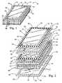
- FIG. 1is a top perspective view of a chip stack constructed in accordance with the present invention
- FIG. 2is an exploded view of the chip stack shown in FIG. 1;
- FIG. 3is an exploded view of the various components which are stacked upon each other in accordance with a preferred method of assembling the chip stack of the present invention
- FIG. 4is a partial cross-sectional view of the components shown in FIG. 3 as stacked upon each other prior to a solder reflow step of the present assembly method;
- FIG. 4 ais an enlargement of the encircled region 4 a shown in FIG. 4;
- FIG. 5is partial cross-sectional view similar to FIG. 4 illustrating the components shown in FIG. 3 as stacked upon each other subsequent to the completion of the solder reflow step of the present assembly method;
- FIG. 5 ais an enlargement of the encircled region 5 a shown in FIG. 5 .
- FIG. 1perspectively illustrates a chip stack 10 assembled in accordance with the present invention.
- the chip stack 10comprises at least two identically configured base layers 12 .
- Each of the base layers 12itself comprises a rectangularly configured base substrate 14 which defines a generally planar top surface 16 , a generally planar bottom surface 18 , an opposed pair of longitudinal peripheral edge segments 20 , and an opposed pair of lateral peripheral edge segments 22 .
- first conductive patternDisposed on the base substrate 14 of each base layer 12 is a first conductive pattern which itself preferably comprises a first set of base pads 24 and a second set of base pads 26 which are each disposed on the top surface 16 of the base substrate 14 .
- the base pads 24 of the first setare preferably arranged in a generally rectangular pattern or array in the central portion of the base substrate 14 , with the base pads 26 of the second set extending linearly along the longitudinal and lateral peripheral edge segments 20 , 22 of the base substrate 14 .
- the base pads 24 of the first setare electrically connected to respective ones of the base pads 26 of the second set via conductive traces 28 .
- the first conductive pattern of each base layer 12comprises a third set of base pads 30 which is disposed on the bottom surface 18 of the base substrate 14 .
- the base pads 30 of the third setare preferably arranged in an identical pattern to the base pads 26 of the second set, and extend linearly along the longitudinal and lateral peripheral edge segments 20 , 22 of the base substrate 14 such that each of the base pads 30 of the third set is aligned with and electrically connected to a respective one of the base pads 26 of the second set.
- each of the base pads 26 of the second setis electrically connected to a respective one of the base pads 30 of the third set via a base feed-through hole 32 .
- Each base feed-through hole 32is preferably plugged with a conductive material.
- the conductive materialis preferably selected from the group consisting of nickel, gold, tin, silver epoxy, and combinations thereof.
- the base pads 26 , 30 of the second and third sets, as well as the base pads 24 of the first set, eacheach preferably have a generally circular configuration. In this respect, each base feed-through hole 32 preferably extends axially between each corresponding, coaxially aligned pair of the base pads 26 , of the second and third sets.
- the base pads 26 , 30 of the second and third setsare preferably formed upon (i.e., surface plated to) the base substrate 14 subsequent to the plugging of the base feed-through holes 32 and are used to cover the opposed, open ends thereof. If the base feed-through holes 32 were left unplugged, solder coming into contact with the base pads 26 , 30 of the second and third sets would tend to wick into the base feed-through holes 32 upon the reflow of the solder (which will be discussed below), thus robbing the base pads 26 , 30 of solder needed to facilitate various electrical connections in the chip stack 10 .
- the chip stack 10 of the present inventioncomprises at least one rectangularly configured interconnect frame 34 .
- the interconnect frame 34defines a generally planar top surface 36 , a generally planar bottom surface 38 , an opposed pair of longitudinal side sections 40 , and an opposed pair of lateral side sections 42 .
- Disposed on the interconnect frame 34is a second conductive pattern which itself preferably comprises a first set of frame pads 44 disposed on the top surface 36 , and a second set of frame pads 46 disposed on the bottom surface 38 .
- the frame pads 44 , 46 of the first and second setsare preferably arranged in patterns which are identical to each other, and to the patterns of the second and third sets of base pads 26 , 30 of each of the base layers 12 .
- the frame pads 44 , 46 of the first and second setseach extend linearly along the longitudinal and lateral side sections 40 , 42 of the interconnect frame 34 , with each of the frame pads 44 of the first set being aligned with and electrically connected to a respective one of the frame pads 46 of the second set.
- the electrical connection of each of the frame pads 44 of the first set to a respective one of the frame pads 46 of the second setis preferably accomplished via a frame feed-through hole 48 which is also preferably plugged with a conductive material.
- the conductive materialis preferably selected from the same group used as the conductive material to plug the base feed-through holes 32 , i.e., nickel, gold, tin, silver epoxy, and combinations thereof.
- Each of the frame feed-through holes 48preferably extends axially between a corresponding, coaxially aligned pair of the frame pads 44 , 46 of the first and second sets, with the plugging of the frame feed-through holes 48 preferably occurring prior to the surface plating of the frame pads 44 , 46 of the first and second sets to respective ones of the top and bottom surfaces 36 , 38 of the interconnect frame 34 .
- the interconnect frame 34is preferably prepared for use in the chip stack 10 by forming generally semi-spherically shaped solder bumps 50 on each of the frame pads 44 , 46 of the first and second sets.
- These solder bumps 50are preferably formed by first stenciling solder paste onto the frame pads 44 , 46 of the first and second sets, and thereafter reflowing the solder paste to form the solder bumps 50 .
- the use of a six mil thick stencil with an aperture approximately the same size as each of the frame pads 44 , 46will facilitate the formation of a solder bump 50 approximately six mils high.
- the frame pads 44 , 46 of the first and second setsare formed (i.e., surface plated) subsequent to the frame feed-through holes 48 being plugged with the conductive material. If the frame feed-through holes 48 were left unplugged, each frame feed-through hole 48 could trap flux or air which would blow out the solder during the reflow cycle used to form the solder bumps 50 on each corresponding, coaxially aligned pair of frame pads 44 , 46 of the first and second sets.
- the interconnect frame 34is disposed between the base layers 12 , with the second conductive pattern of the interconnect frame 34 being electrically connected to the first conductive pattern of each of the base layers 12 .
- the frame pads 46 of the second setare electrically connected to respective ones of the base pads 26 of the second set of one of the base layers 12 (i.e., the base layer 12 immediately below the interconnect frame 34 in the chip stack 10 ), with the frame pads 44 of the first set being electrically connected to respective ones of the base pads of the third set of one of the base layers 12 (i.e., the base layer 12 immediately above the interconnect frame 34 in the chip stack 10 ).
- each coaxially aligned pair of frame pads 44 , 46 of the first and second setsis itself coaxially aligned with a coaxially aligned set of base pads 26 , 30 of the second and third sets of each of the adjacent base layers 12 .
- the electrical connection of the second conductive pattern of the interconnect frame 34 to the first conductive pattern of each of the adjacent base layers 12is preferably facilitated via a soldering process which will be described in more detail below.
- the chip stack 10 of the present inventionfurther preferably comprises a transposer layer 52 .
- the transposer layer 52itself comprises a rectangularly configured transposer substrate 54 which defines a generally planar top surface 56 , a generally planar bottom surface 58 , an opposed pair of longitudinal peripheral edge segments 60 , and an opposed pair of lateral peripheral edge segments 62 .
- Disposed on the transposer substrate 54is a third conductive pattern.
- the third conductive patterncomprises a first set of transposer pads 64 which are disposed on the top surface 56 of the transposer substrate 54 , and a second set of transposer pads 66 which are disposed on the bottom surface 58 thereof.
- the transposer pads 64 of the first setare electrically connected to respective ones of the transposer pads 66 of the second set via conductive traces.
- the transposer pads 64 of the first setare preferably arranged in a pattern which is identical to the patterns of the second and third sets of base pads 26 , 30 and the first and second sets of frame pads 44 , 46 .
- the transposer pads 64 of the first setextend linearly along the longitudinal and lateral peripheral edge segments 60 , 62 of the transposer substrate 54 .
- the transposer pads 66 of the second setare themselves preferably arranged in a generally rectangular pattern or array in the central portion of the bottom surface 58 of the transposer substrate 54 , with the pattern of the transposer pads 66 of the second set preferably being identical to the pattern of the base pads 24 of the first set of each of the base layers 12 .
- the transposer layer 52is prepared for use in the chip stack 10 by forming generally spherically shaped solder balls 68 on each of the transposer pads 66 of the second set.
- These solder balls 68are preferably formed by stencil printing solder paste onto each of the transposer pads 66 of the second set, and thereafter reflowing the solder paste to form the solder balls 68 .
- the aperture in the stencil used to form the solder balls 68is typically larger than each of the transposer pads 66 and thick enough to deposit sufficient solder to form the solder balls 68 . As seen in FIG.
- the transposer layer 52is also prepared for use in the chip stack 10 by forming generally semi-spherically shaped solder bumps 67 on each of the transposer pads 64 of the first set. These solder bumps 67 are preferably formed in the same manner previously described in relation to the formation of the solder bumps 50 on the frame pads 44 , 46 of the first and second sets.
- the first conductive pattern of one of the base layers 12is electrically connected to the third conductive pattern of the transposer layer 52 . More particularly, each of the base pads 30 of the third set of the lowermost base layer 12 is electrically connected to a respective one of the transposer pads 64 of the first set. Due to the base pads 30 of the third set and the transposer pads 64 of the first set being arranged in identical patterns, each of the base pads 30 of third set is coaxially alignable with a respective one of the transposer pads 64 of the first set, with the electrical connection therebetween preferably being facilitated via soldering as will be discussed in more detail below.
- the base pads 24 , 26 , 30 of the first, second and third sets, the conductive traces 28 , the frame pads 44 , 46 of the first and second sets, and the transposer pads 64 , 66 of the first and second setsare each preferably fabricated from very thin copper having a thickness in the range of from about five microns to about twenty-five microns through the use of conventional etching techniques.
- the use of thin copper for the various pads and traces 28allows for etching line widths and spacings down to a pitch of about 4 mils which substantially increases the routing density on each of the base layers 12 , as well as the transposer layer 52 .
- the base substrate 14 , the interconnect frame 34 , and the transposer substrate 54are each preferably fabricated from either FR-4, polyamide, or some other suitable material which can easily be routed. As indicated above, all of the base feed-through holes 32 and frame feed-through holes 48 are plugged with a conductive material prior to the surface plating procedure used to form the base pads 24 , 26 , 30 of the first, second and third sets, and the frame pads 44 , 46 of the first and second sets.
- the material used to form each base substrate 14 and/or the transposer substrate 54may be as thin as about 0.010 inches or may be a thicker multilayer structure.
- the chip stack 10 of the present inventionfurther comprises at least two identically configured integrated circuit chips 70 which are electrically connected to respective ones of the first conductive patterns of the base layers 12 .
- Each of the integrated circuit chips 70preferably comprises a rectangularly configured body 72 defining a generally planar top surface 74 , a generally planar bottom surface 76 , an opposed pair of longitudinal sides 78 , and an opposed pair of lateral sides 80 .
- Disposed on the bottom surface 76 of the body 72are a plurality of generally spherically shaped conductive contacts 82 which are preferably arranged in a pattern identical to the patterns of the base pads 24 of the first set and the transposer pads 66 of the second set.
- the conductive contacts 82 of each of the integrated circuit chips 70are electrically connected to respective ones of the base pads 24 of the first set of a respective one of the first conductive patterns of the base layers 12 . Due to the conductive contacts 82 and base pads 24 of each of the first sets being arranged in identical patterns, the conductive contacts 82 of each of the integrated circuit chips 70 are coaxially alignable with respective ones of the base pads 24 of the corresponding first set. In each of the integrated circuit chips 70 , solder is preferably pre-applied to each of the conductive contacts 82 thereof.
- each of the integrated circuit chips 70is preferably a BGA (ball grid array) device, though the same may alternatively comprise either a CSP device or a flip chip device.
- BGAball grid array
- a layer 84 of flux/underfillis preferably disposed between the bottom surface 76 of the body 72 of each of the integrated circuit chips 70 and respective ones of the top surfaces 16 of the base substrates 14 .
- Each layer 84 of the flux/underfillis preferably spread over the base pads 24 of the first set of a respective one of the first conductive patterns of the base layers 12 .
- Each layer 84substantially encapsulates the conductive contacts 82 of the corresponding integrated circuit chip 70 when the same is electrically connected to the first conductive pattern of a respective one of the base layers 12 .
- a bakeout cycleis required to drive out the moisture in the base layer 12 and the corresponding integrated circuit chip 70 .
- a cycle of approximately eight hours at about 125° Celsiusis desirable, which is followed by storage in a dry nitrogen atmosphere until use.
- the first step in the attachment of the integrated circuit chip 70 to the corresponding base layer 12is the precise deposition of the layer 84 of an appropriate flux/underfill material over the base pads 24 of the corresponding first set.
- the integrated circuit chip 70is then placed over the pad area, squeezing out the flux/underfill material of the layer 84 to the longitudinal and lateral sides 78 , 80 of the body 72 and seating the conductive contacts 82 onto respective ones of the base pads 24 of the corresponding first set. If done properly, the layer 84 of the flux/underfill material, when cured, will have no voids or minimum voids.
- the base layer 12 having the integrated circuit chip 70 positioned thereupon in the above-described manneris then run through a solder reflow cycle with no dwelling time at an intermediate temperature of approximately 150° Celsius. A post cure cycle to complete the polymerization of the layer 84 of the flux/underfill material may be required depending on the particular flux/underfill material used in the layer 84 . At this juncture, the base layer 12 having the integrated circuit chip 70 electrically connected thereto may be electrically tested.
- the standard approach for the attachment or electrical connection of the conductive contacts of a BGA device to an attachment or pad siteis to first flux the pad site or conductive contacts of the BGA device, place the BGA device on the pad site in the proper orientation, reflow the solder pre-applied to the conductive contacts of the BGA device to facilitate the electrical connection to the pad site, clean, then underfill and cure.
- the cleaning steptypically requires considerable time since the gap under the bottom surface of the body of the BGA device is very small and very difficult to penetrate with standard cleaning methods. Also, the removal of the cleaning fluid (which is generally water) requires long bakeout times.
- the underfill of an epoxy between the bottom surface of the body of the BGA device and the top surface of the substrate having the pad site thereonis a relatively easy procedure, but is very slow. If a no-clean flux is used for attachment, the residue from the flux typically becomes entrapped within the epoxy underfill and may cause corrosion problems. A subsequent solder reflow process to facilitate the attachment of the chip stack to a main printed circuit board (PCB) often causes the residue flux to vaporize which exerts pressure on the solder joints and could delaminate the structure. Most underfill materials become very hard (i.e., greater than ninety shore D) and are cured at a temperature of less than about 180° Celsius.
- solderis solid at this temperature and the underfill encases the solder with no room for expansion.
- the solder from the conductive contacts of the BGA deviceexpands when molten again, thus exerting pressure which can delaminate the structure. If the chip stack is not subjected to subsequent reflow temperatures when completed, there is no problem. However, the chip stack must be able to withstand the subsequent reflow temperature.
- the flux/underfill material used for the layer 84provides both flux and underfill properties with one formulation. As the temperature rises during the solder reflow process which will be discussed below, the flux characteristics of the material aid in the solder process, with extended exposure to the peak solder reflow temperature beginning the polymerization process of the underfill portion of the material. The flux is incorporated into the underfill, thus becoming one compatible material which is cured above the melting point of solder. Thus, there is room within the encased solder for expansion at the reflow temperature. No cleaning steps are required, though careful dispensing of the correct volume and accurate placement of the integrated circuit chip 70 upon its corresponding base layer 12 is critical.
- the complete chip stack 10 shown in FIG. 1includes a transposer layer 52 , four base layers 12 , three interconnect frames 34 , and four integrated circuit chips 70 .
- the first conductive pattern of the lowermost base layer 12is electrically connected to the third conductive pattern of the transposer layer 52 in the above-described manner.
- each of the interconnect frames 34is disposed or positioned between an adjacent pair of base layers 12 , with the second conductive pattern of each of the interconnect frames 34 being electrically connected to the first conductive pattern of such adjacent pair of base layers 12 in the above-described manner.
- the integrated circuit chips 70 other than for the uppermost integrated circuit chip 70are disposed between adjacent pairs of the base layers 12 and are each circumvented by a respective one of the interconnect frames 34 .
- the bodies 72 of the integrated circuit chips 70 and the interconnect frames 34are preferably sized relative to each other such that the top surface 74 of the body 72 of an integrated circuit chip 70 which is circumvented by an interconnect frame 34 does not protrude beyond the top surface 36 thereof.
- the various electrical connections within the chip stack 10are preferably facilitated via soldering.
- the transposer pads 66 of the second setwhich are spherically shaped as indicated above, form a ball grid array on the bottom of the chip stack 10 which is specifically suited for facilitating the attachment of the chip stack 10 to a printed circuit board (PCB).
- PCBprinted circuit board
- the chip stack 10may be assembled to include fewer or greater than four base layers 12 , three interconnect frames 34 , and four integrated circuit chips 70 .
- multiple chip stacks 10may be concurrently assembled through the use of a transposer panel 86 , at least two base panels 88 , at least one frame panel 90 , at least three spacer-sheets 92 , and a plurality of integrated circuit chips 70 .
- the transposer panel 86is formed to include multiple groups of the first and second sets of transposer pads 64 , 66 with such groups being formed on the transposer panel 86 in spaced relation to each other.
- each of the base panels 88is formed to include multiple groups of the first, second and third sets of base pads 24 , 26 , 30 , with the frame panels 90 each being formed to include multiple groups of the first and second sets of frame pads 44 , 46 .
- the transposer panel 86is prepared such that the transposer pads 64 of the first set of each group have the solder bumps 67 formed thereon, with the transposer pads 66 of the second set of each group having the solder balls 68 formed thereon.
- each of the frame panels 90is prepared such that the first and second sets of frame pads 44 , 46 of each group have the solder bumps 50 formed thereon.
- the spacer sheets 92are each formed to define a plurality of rectangularly configured openings 94 , the length and width dimensions of which exceed those of the base and transposer substrates 14 , 54 and interconnect frames 34 which are substantially equal to each other.
- the integrated circuit chips 70are electrically connected to respective ones of each of the first sets of base pads 24 included on each of the base panels 88 . Such electrical connection is accomplished in the above-described manner. Subsequent to the pre-attachment of the integrated circuit chips 70 to the base panels 88 , flux/underfill material is dispensed onto each of the solder bumps 67 of the transposer panel 86 , with the flux/underfill material also being dispensed onto all of the solder bumps 50 of each of the frame panels 90 . The transposer panel is then cooperatively engaged to a stacking fixture such that the solder balls 68 face or are directed downwardly.
- a spacer sheet 92is then stacked upon the transposer panel 86 such that the transposer pads 64 of the first set of each group are aligned with respective ones of the openings 94 within the spacer sheet 92 .
- a base panel 88is then stacked upon the spacer sheet 92 such that the base pads 30 of the third set of each group face or are directed downwardly and are aligned with respective ones of the openings 94 and respective ones of the transposer pads 64 of the first set of the corresponding group upon the transposer panel 86 immediately therebelow.
- Another spacer sheet 92is then stacked upon the base panel 88 such that the base pads 24 , 26 of the first and second sets of each group are aligned with respective ones of the openings 94 .
- a frame panel 90is stacked upon the uppermost spacer sheet 92 such that the bodies 72 of the integrated circuit chips 70 are each circumvented by the frame panel 90 .
- Another spacer sheet 92is then stacked upon the frame panel 90 such that the frame pads 44 of the first set of each group are aligned with respective ones of the openings 94 .
- Another base panel 88is then stacked upon the uppermost spacer sheet 92 in a manner wherein the base pads 30 of the third set of each group of such uppermost base panel 88 are aligned with respective ones of the openings 94 and respective ones of the frame pads 44 of the first set of the corresponding group upon the frame panel 90 immediately therebelow.
- the above-described stacking processmay be continued or repeated to form a chip stack having a greater number of electrically interconnected integrated circuit chips 70 .
- a pressure plateis applied to the top of the stack to maintain such panels and sheets in prescribed orientations relative to each other.
- the stacked panels and sheetsare then subjected to heat at a level sufficient to facilitate the reflow of the solder bumps 50 , 67 .
- the solder reflow cycleis typically conducted in a temperature range of from about 215° Celsius to about 250° Celsius.
- the individual chip stacksare separated through the use of a router.
- the spacer sheets 92are needed only for the solder reflow process, and do not become part of each resultant chip stack formed by the completion of the routing process.
- the solder bumps 50 , 67are slightly higher than each spacer sheet 92 . Since light pressure is applied to the various panels and sheets during the solder reflow process, the solder bumps 50 , 67 collapse, thus making the appropriate electrical connections to the corresponding pads (i.e., the base pads 26 , 30 of either the second or third sets).
- the spacer sheets 92keep the solder from being squeezed out and bridging to neighboring pads.
- a spacing of from about four mils to about six milscan be accomplished using spacer sheets 92 which are fabricated from paper.
- the papercan be easily punched to form the openings 94 , does not interfere with the routing process, can withstand the solder reflow temperature in the aforementioned range, and is inexpensive.
- the paper spacer sheets 92would be sized the same as the transposer, base and frame panels 86 , 88 , 90 , and punched to include openings 94 which are slightly larger than the finished, routed chip stack. With slight pressure being applied to the stacked panels and sheets, the space between the panels and sheets is easily maintained, thus eliminating the necessity to remove the spacer sheets 92 subsequent to the reflow of the solder. As indicated above, the paper spacer sheets 92 would not interfere with the routing process, and would be removed with the rest of the debris.
- the present assembly methodhas high volume potential, with the use of the flux/underfill material providing localized encapsulation of the conductive contacts 82 of the integrated circuit chips 70 and eliminating the need for a cleaning cycle as discussed above.
- a transposer panel 86need not necessarily be included in the assembly process, since the lowermost base layer 12 in any chip stack may be used as a transposer board to facilitate the mounting or electrical connection of the chip stack to a PCB.
- the solder joints between each of the integrated circuit chips 70 and the corresponding base layer 12are protected by the flux/underfill material.
Landscapes
- Engineering & Computer Science (AREA)
- Microelectronics & Electronic Packaging (AREA)
- Power Engineering (AREA)
- Physics & Mathematics (AREA)
- Condensed Matter Physics & Semiconductors (AREA)
- General Physics & Mathematics (AREA)
- Computer Hardware Design (AREA)
- Wire Bonding (AREA)
- Structures For Mounting Electric Components On Printed Circuit Boards (AREA)
Abstract
Description
Claims (8)
Priority Applications (2)
| Application Number | Priority Date | Filing Date | Title |
|---|---|---|---|
| US09/922,977US6544815B2 (en) | 2000-06-21 | 2001-08-06 | Panel stacking of BGA devices to form three-dimensional modules |
| US10/290,994US20030064548A1 (en) | 2000-06-21 | 2002-11-08 | Panel stacking of BGA devices to form three-dimensional modules |
Applications Claiming Priority (2)
| Application Number | Priority Date | Filing Date | Title |
|---|---|---|---|
| US09/598,343US6404043B1 (en) | 2000-06-21 | 2000-06-21 | Panel stacking of BGA devices to form three-dimensional modules |
| US09/922,977US6544815B2 (en) | 2000-06-21 | 2001-08-06 | Panel stacking of BGA devices to form three-dimensional modules |
Related Parent Applications (1)
| Application Number | Title | Priority Date | Filing Date |
|---|---|---|---|
| US09/598,343DivisionUS6404043B1 (en) | 2000-06-21 | 2000-06-21 | Panel stacking of BGA devices to form three-dimensional modules |
Related Child Applications (1)
| Application Number | Title | Priority Date | Filing Date |
|---|---|---|---|
| US10/290,994ContinuationUS20030064548A1 (en) | 2000-06-21 | 2002-11-08 | Panel stacking of BGA devices to form three-dimensional modules |
Publications (2)
| Publication Number | Publication Date |
|---|---|
| US20010054770A1 US20010054770A1 (en) | 2001-12-27 |
| US6544815B2true US6544815B2 (en) | 2003-04-08 |
Family
ID=24395181
Family Applications (7)
| Application Number | Title | Priority Date | Filing Date |
|---|---|---|---|
| US09/598,343Expired - LifetimeUS6404043B1 (en) | 2000-06-21 | 2000-06-21 | Panel stacking of BGA devices to form three-dimensional modules |
| US09/826,621Expired - LifetimeUS6472735B2 (en) | 2000-06-21 | 2001-04-05 | Three-dimensional memory stacking using anisotropic epoxy interconnections |
| US09/922,977Expired - LifetimeUS6544815B2 (en) | 2000-06-21 | 2001-08-06 | Panel stacking of BGA devices to form three-dimensional modules |
| US10/017,553Expired - LifetimeUS6566746B2 (en) | 2000-06-21 | 2001-12-14 | Panel stacking of BGA devices to form three-dimensional modules |
| US10/092,073AbandonedUS20020094603A1 (en) | 2000-06-21 | 2002-03-06 | Three-dimensional memory stacking using anisotropic epoxy interconnections |
| US10/290,994AbandonedUS20030064548A1 (en) | 2000-06-21 | 2002-11-08 | Panel stacking of BGA devices to form three-dimensional modules |
| US10/316,566Expired - LifetimeUS6878571B2 (en) | 2000-06-21 | 2002-12-11 | Panel stacking of BGA devices to form three-dimensional modules |
Family Applications Before (2)
| Application Number | Title | Priority Date | Filing Date |
|---|---|---|---|
| US09/598,343Expired - LifetimeUS6404043B1 (en) | 2000-06-21 | 2000-06-21 | Panel stacking of BGA devices to form three-dimensional modules |
| US09/826,621Expired - LifetimeUS6472735B2 (en) | 2000-06-21 | 2001-04-05 | Three-dimensional memory stacking using anisotropic epoxy interconnections |
Family Applications After (4)
| Application Number | Title | Priority Date | Filing Date |
|---|---|---|---|
| US10/017,553Expired - LifetimeUS6566746B2 (en) | 2000-06-21 | 2001-12-14 | Panel stacking of BGA devices to form three-dimensional modules |
| US10/092,073AbandonedUS20020094603A1 (en) | 2000-06-21 | 2002-03-06 | Three-dimensional memory stacking using anisotropic epoxy interconnections |
| US10/290,994AbandonedUS20030064548A1 (en) | 2000-06-21 | 2002-11-08 | Panel stacking of BGA devices to form three-dimensional modules |
| US10/316,566Expired - LifetimeUS6878571B2 (en) | 2000-06-21 | 2002-12-11 | Panel stacking of BGA devices to form three-dimensional modules |
Country Status (2)
| Country | Link |
|---|---|
| US (7) | US6404043B1 (en) |
| WO (1) | WO2001099187A1 (en) |
Cited By (30)
| Publication number | Priority date | Publication date | Assignee | Title |
|---|---|---|---|---|
| US20030064548A1 (en)* | 2000-06-21 | 2003-04-03 | Isaak Harlan R. | Panel stacking of BGA devices to form three-dimensional modules |
| US20030113951A1 (en)* | 2001-12-19 | 2003-06-19 | Via Technologies, Inc. | Method for manufacturing multi-layer package substrates |
| US20040108584A1 (en)* | 2002-12-05 | 2004-06-10 | Roeters Glen E. | Thin scale outline package |
| US20040207990A1 (en)* | 2003-04-21 | 2004-10-21 | Rose Andrew C. | Stair-step signal routing |
| US20060053345A1 (en)* | 2004-09-03 | 2006-03-09 | Staktek Group L.P. | Thin module system and method |
| US20060050498A1 (en)* | 2004-09-03 | 2006-03-09 | Staktek Group L.P. | Die module system and method |
| US7033861B1 (en) | 2005-05-18 | 2006-04-25 | Staktek Group L.P. | Stacked module systems and method |
| US20060250780A1 (en)* | 2005-05-06 | 2006-11-09 | Staktek Group L.P. | System component interposer |
| US7193310B2 (en) | 2001-12-14 | 2007-03-20 | Stuktek Group L.P. | Stacking system and method |
| US7202555B2 (en) | 2001-10-26 | 2007-04-10 | Staktek Group L.P. | Pitch change and chip scale stacking system and method |
| US7289327B2 (en) | 2006-02-27 | 2007-10-30 | Stakick Group L.P. | Active cooling methods and apparatus for modules |
| US7324352B2 (en) | 2004-09-03 | 2008-01-29 | Staktek Group L.P. | High capacity thin module system and method |
| US7443023B2 (en) | 2004-09-03 | 2008-10-28 | Entorian Technologies, Lp | High capacity thin module system |
| US7446410B2 (en) | 2004-09-03 | 2008-11-04 | Entorian Technologies, Lp | Circuit module with thermal casing systems |
| US7468893B2 (en) | 2004-09-03 | 2008-12-23 | Entorian Technologies, Lp | Thin module system and method |
| CN100447954C (en)* | 2005-10-31 | 2008-12-31 | 胜开科技股份有限公司 | Method for manufacturing metal balls of ball grid array of semiconductor component |
| US7480152B2 (en) | 2004-09-03 | 2009-01-20 | Entorian Technologies, Lp | Thin module system and method |
| US7511969B2 (en) | 2006-02-02 | 2009-03-31 | Entorian Technologies, Lp | Composite core circuit module system and method |
| US7511968B2 (en) | 2004-09-03 | 2009-03-31 | Entorian Technologies, Lp | Buffered thin module system and method |
| US7522421B2 (en) | 2004-09-03 | 2009-04-21 | Entorian Technologies, Lp | Split core circuit module |
| US7542297B2 (en) | 2004-09-03 | 2009-06-02 | Entorian Technologies, Lp | Optimized mounting area circuit module system and method |
| US7579687B2 (en) | 2004-09-03 | 2009-08-25 | Entorian Technologies, Lp | Circuit module turbulence enhancement systems and methods |
| US20090218675A1 (en)* | 2005-04-11 | 2009-09-03 | Hyeog Chan Kwon | Multipackage module having stacked packages with asymmetrically arranged die and molding |
| US7595550B2 (en) | 2001-10-26 | 2009-09-29 | Entorian Technologies, Lp | Flex-based circuit module |
| US7606040B2 (en) | 2004-09-03 | 2009-10-20 | Entorian Technologies, Lp | Memory module system and method |
| US7606050B2 (en) | 2004-09-03 | 2009-10-20 | Entorian Technologies, Lp | Compact module system and method |
| US7606049B2 (en) | 2004-09-03 | 2009-10-20 | Entorian Technologies, Lp | Module thermal management system and method |
| US7616452B2 (en) | 2004-09-03 | 2009-11-10 | Entorian Technologies, Lp | Flex circuit constructions for high capacity circuit module systems and methods |
| US7656678B2 (en) | 2001-10-26 | 2010-02-02 | Entorian Technologies, Lp | Stacked module systems |
| US7760513B2 (en) | 2004-09-03 | 2010-07-20 | Entorian Technologies Lp | Modified core for circuit module system and method |
Families Citing this family (357)
| Publication number | Priority date | Publication date | Assignee | Title |
|---|---|---|---|---|
| US6525414B2 (en)* | 1997-09-16 | 2003-02-25 | Matsushita Electric Industrial Co., Ltd. | Semiconductor device including a wiring board and semiconductor elements mounted thereon |
| US7332375B1 (en) | 1998-06-24 | 2008-02-19 | Amkor Technology, Inc. | Method of making an integrated circuit package |
| US6143981A (en) | 1998-06-24 | 2000-11-07 | Amkor Technology, Inc. | Plastic integrated circuit package and method and leadframe for making the package |
| EP1196014B1 (en)* | 1999-07-09 | 2006-01-04 | Fujitsu Limited | Printed wiring board unit, hierarchical mounting auxiliary substrate and electronic apparatus |
| TW472330B (en)* | 1999-08-26 | 2002-01-11 | Toshiba Corp | Semiconductor device and the manufacturing method thereof |
| US6713854B1 (en) | 2000-10-16 | 2004-03-30 | Legacy Electronics, Inc | Electronic circuit module with a carrier having a mounting pad array |
| US7102892B2 (en)* | 2000-03-13 | 2006-09-05 | Legacy Electronics, Inc. | Modular integrated circuit chip carrier |
| GB0012420D0 (en)* | 2000-05-24 | 2000-07-12 | Ibm | Microcard interposer |
| US7298031B1 (en)* | 2000-08-09 | 2007-11-20 | Micron Technology, Inc. | Multiple substrate microelectronic devices and methods of manufacture |
| US6607937B1 (en)* | 2000-08-23 | 2003-08-19 | Micron Technology, Inc. | Stacked microelectronic dies and methods for stacking microelectronic dies |
| WO2002030069A1 (en)* | 2000-10-06 | 2002-04-11 | Irvine Sensors Corporation | High speed multi-stage stacked layers switch |
| US7337522B2 (en)* | 2000-10-16 | 2008-03-04 | Legacy Electronics, Inc. | Method and apparatus for fabricating a circuit board with a three dimensional surface mounted array of semiconductor chips |
| JP2002251884A (en)* | 2001-02-21 | 2002-09-06 | Toshiba Corp | Semiconductor memory device and system device thereof |
| EP1367875A4 (en)* | 2001-03-07 | 2008-07-30 | Sony Corp | Land portion of printed wiring board, method for manufacturing printed wiring board, and printed wiring board mounting method |
| WO2002074024A2 (en)* | 2001-03-14 | 2002-09-19 | Legacy Electronics, Inc. | A method and apparatus for fabricating a circuit board with a three dimensional surface mounted array of semiconductor chips |
| US7034386B2 (en)* | 2001-03-26 | 2006-04-25 | Nec Corporation | Thin planar semiconductor device having electrodes on both surfaces and method of fabricating same |
| KR100369393B1 (en) | 2001-03-27 | 2003-02-05 | 앰코 테크놀로지 코리아 주식회사 | Lead frame and semiconductor package using it and its manufacturing method |
| JP4051893B2 (en)* | 2001-04-18 | 2008-02-27 | 株式会社日立製作所 | Electronics |
| JP3999945B2 (en)* | 2001-05-18 | 2007-10-31 | 株式会社東芝 | Manufacturing method of semiconductor device |
| US6730536B1 (en) | 2001-06-28 | 2004-05-04 | Amkor Technology, Inc. | Pre-drilled image sensor package fabrication method |
| US6433413B1 (en)* | 2001-08-17 | 2002-08-13 | Micron Technology, Inc. | Three-dimensional multichip module |
| US6747347B2 (en)* | 2001-08-30 | 2004-06-08 | Micron Technology, Inc. | Multi-chip electronic package and cooling system |
| JP2003110091A (en)* | 2001-09-28 | 2003-04-11 | Toshiba Corp | Semiconductor device and method of manufacturing semiconductor device |
| JP2003179099A (en)* | 2001-12-12 | 2003-06-27 | Toshiba Corp | Semiconductor device and method of manufacturing the same |
| US6891276B1 (en)* | 2002-01-09 | 2005-05-10 | Bridge Semiconductor Corporation | Semiconductor package device |
| EP1472730A4 (en)* | 2002-01-16 | 2010-04-14 | Mann Alfred E Found Scient Res | HOUSING FOR ELECTRONIC CIRCUITS WITH REDUCED SIZE |
| FI119215B (en)* | 2002-01-31 | 2008-08-29 | Imbera Electronics Oy | A method for immersing a component in a substrate and an electronic module |
| US8455994B2 (en)* | 2002-01-31 | 2013-06-04 | Imbera Electronics Oy | Electronic module with feed through conductor between wiring patterns |
| US6635970B2 (en)* | 2002-02-06 | 2003-10-21 | International Business Machines Corporation | Power distribution design method for stacked flip-chip packages |
| US7242082B2 (en) | 2002-02-07 | 2007-07-10 | Irvine Sensors Corp. | Stackable layer containing ball grid array package |
| US6657311B1 (en)* | 2002-05-16 | 2003-12-02 | Texas Instruments Incorporated | Heat dissipating flip-chip ball grid array |
| KR20040022063A (en)* | 2002-09-06 | 2004-03-11 | 주식회사 유니세미콘 | A stack semiconductor package and it's manufacture method |
| TWI290365B (en)* | 2002-10-15 | 2007-11-21 | United Test Ct Inc | Stacked flip-chip package |
| TW567601B (en)* | 2002-10-18 | 2003-12-21 | Siliconware Precision Industries Co Ltd | Module device of stacked semiconductor package and method for fabricating the same |
| US7723210B2 (en) | 2002-11-08 | 2010-05-25 | Amkor Technology, Inc. | Direct-write wafer level chip scale package |
| US6905914B1 (en) | 2002-11-08 | 2005-06-14 | Amkor Technology, Inc. | Wafer level package and fabrication method |
| JP4035034B2 (en)* | 2002-11-29 | 2008-01-16 | 株式会社ルネサステクノロジ | Semiconductor device and manufacturing method thereof |
| US6841883B1 (en)* | 2003-03-31 | 2005-01-11 | Micron Technology, Inc. | Multi-dice chip scale semiconductor components and wafer level methods of fabrication |
| US7145226B2 (en)* | 2003-06-30 | 2006-12-05 | Intel Corporation | Scalable microelectronic package using conductive risers |
| DE10334575B4 (en)* | 2003-07-28 | 2007-10-04 | Infineon Technologies Ag | Electronic component and use and method for producing the same |
| AU2003261429A1 (en)* | 2003-08-08 | 2005-03-07 | Irvine Sensors Corporation | Stackable layers containing ball grid array packages |
| FI20031341L (en)* | 2003-09-18 | 2005-03-19 | Imbera Electronics Oy | Method for manufacturing an electronic module |
| US7425759B1 (en)* | 2003-11-20 | 2008-09-16 | Bridge Semiconductor Corporation | Semiconductor chip assembly with bumped terminal and filler |
| US7095104B2 (en)* | 2003-11-21 | 2006-08-22 | International Business Machines Corporation | Overlap stacking of center bus bonded memory chips for double density and method of manufacturing the same |
| DE10360708B4 (en)* | 2003-12-19 | 2008-04-10 | Infineon Technologies Ag | Semiconductor module with a semiconductor stack, rewiring plate, and method of making the same |
| US7126829B1 (en)* | 2004-02-09 | 2006-10-24 | Pericom Semiconductor Corp. | Adapter board for stacking Ball-Grid-Array (BGA) chips |
| US7345359B2 (en)* | 2004-03-05 | 2008-03-18 | Intel Corporation | Integrated circuit package with chip-side signal connections |
| WO2005114729A1 (en)* | 2004-05-21 | 2005-12-01 | Nec Corporation | Semiconductor device and wiring board |
| JP2006041438A (en)* | 2004-07-30 | 2006-02-09 | Shinko Electric Ind Co Ltd | Semiconductor chip built-in substrate, and its manufacturing method |
| KR100669830B1 (en)* | 2004-11-16 | 2007-04-16 | 삼성전자주식회사 | Multilayer Package Using Anisotropic Conductive Film |
| US20060108676A1 (en)* | 2004-11-22 | 2006-05-25 | Punzalan Nelson V Jr | Multi-chip package using an interposer |
| JP4433298B2 (en)* | 2004-12-16 | 2010-03-17 | パナソニック株式会社 | Multistage semiconductor module |
| JP4504798B2 (en)* | 2004-12-16 | 2010-07-14 | パナソニック株式会社 | Multistage semiconductor module |
| WO2006076381A2 (en)* | 2005-01-12 | 2006-07-20 | Legacy Electronics, Inc. | Radial circuit board, system, and methods |
| US7745912B2 (en)* | 2005-03-25 | 2010-06-29 | Intel Corporation | Stress absorption layer and cylinder solder joint method and apparatus |
| JP4520355B2 (en)* | 2005-04-19 | 2010-08-04 | パナソニック株式会社 | Semiconductor module |
| TWI284394B (en)* | 2005-05-12 | 2007-07-21 | Advanced Semiconductor Eng | Lid used in package structure and the package structure of having the same |
| US7777313B2 (en)* | 2005-06-07 | 2010-08-17 | Analog Devices, Inc. | Electronic package structures and methods |
| WO2007003228A1 (en)* | 2005-06-30 | 2007-01-11 | Siemens Aktiengesellschaft | Hardware protection system for sensitive electronic-data modules protecting against external manipulations |
| CN101253821B (en)* | 2005-06-30 | 2011-01-26 | 西门子公司 | Sensors for hardware protection of sensitive electronic data components from external manipulation |
| US7785928B2 (en)* | 2005-07-09 | 2010-08-31 | Gautham Viswanadam | Integrated circuit device and method of manufacturing thereof |
| US7576995B2 (en) | 2005-11-04 | 2009-08-18 | Entorian Technologies, Lp | Flex circuit apparatus and method for adding capacitance while conserving circuit board surface area |
| CN100541784C (en)* | 2005-11-10 | 2009-09-16 | 沈育浓 | Stacked semiconductor chip package |
| CN100552940C (en)* | 2005-11-25 | 2009-10-21 | 全懋精密科技股份有限公司 | Stack structure of semiconductor element embedded loading board |
| US7507603B1 (en) | 2005-12-02 | 2009-03-24 | Amkor Technology, Inc. | Etch singulated semiconductor package |
| US7572681B1 (en)* | 2005-12-08 | 2009-08-11 | Amkor Technology, Inc. | Embedded electronic component package |
| US7332799B2 (en)* | 2005-12-28 | 2008-02-19 | Tessera, Inc. | Packaged chip having features for improved signal transmission on the package |
| US7605454B2 (en) | 2006-01-11 | 2009-10-20 | Entorian Technologies, Lp | Memory card and method for devising |
| US7508069B2 (en) | 2006-01-11 | 2009-03-24 | Entorian Technologies, Lp | Managed memory component |
| US7304382B2 (en) | 2006-01-11 | 2007-12-04 | Staktek Group L.P. | Managed memory component |
| US7608920B2 (en) | 2006-01-11 | 2009-10-27 | Entorian Technologies, Lp | Memory card and method for devising |
| US7508058B2 (en) | 2006-01-11 | 2009-03-24 | Entorian Technologies, Lp | Stacked integrated circuit module |
| US7902660B1 (en) | 2006-05-24 | 2011-03-08 | Amkor Technology, Inc. | Substrate for semiconductor device and manufacturing method thereof |
| JP2007324354A (en)* | 2006-05-31 | 2007-12-13 | Sony Corp | Semiconductor device |
| US7968998B1 (en) | 2006-06-21 | 2011-06-28 | Amkor Technology, Inc. | Side leaded, bottom exposed pad and bottom exposed lead fusion quad flat semiconductor package |
| US7468553B2 (en) | 2006-10-20 | 2008-12-23 | Entorian Technologies, Lp | Stackable micropackages and stacked modules |
| US20080150132A1 (en)* | 2006-12-21 | 2008-06-26 | Tom Hu | Stack up pcb substrate for high density interconnect packages |
| SG146460A1 (en)* | 2007-03-12 | 2008-10-30 | Micron Technology Inc | Apparatus for packaging semiconductor devices, packaged semiconductor components, methods of manufacturing apparatus for packaging semiconductor devices, and methods of manufacturing semiconductor components |
| CN101266965B (en)* | 2007-03-15 | 2010-06-16 | 卓恩民 | Semiconductor package stacking structure and manufacturing method thereof |
| WO2008117213A2 (en)* | 2007-03-23 | 2008-10-02 | Koninklijke Philips Electronics N.V. | An assembly of at least two printed circuit boards and a method of assembling at least two printed circuit boards |
| US20080241991A1 (en)* | 2007-03-26 | 2008-10-02 | National Semiconductor Corporation | Gang flipping for flip-chip packaging |
| ITMI20070933A1 (en)* | 2007-05-08 | 2008-11-09 | St Microelectronics Srl | MULTI PIASTRINA ELECTRONIC SYSTEM |
| JP2008306105A (en)* | 2007-06-11 | 2008-12-18 | Oki Electric Ind Co Ltd | Method for manufacturing semiconductor device |
| JP4986738B2 (en)* | 2007-06-27 | 2012-07-25 | 新光電気工業株式会社 | Semiconductor package and semiconductor device using the same |
| US7714426B1 (en) | 2007-07-07 | 2010-05-11 | Keith Gann | Ball grid array package format layers and structure |
| US7977774B2 (en) | 2007-07-10 | 2011-07-12 | Amkor Technology, Inc. | Fusion quad flat semiconductor package |
| US7687899B1 (en)* | 2007-08-07 | 2010-03-30 | Amkor Technology, Inc. | Dual laminate package structure with embedded elements |
| US7619305B2 (en)* | 2007-08-15 | 2009-11-17 | Powertech Technology Inc. | Semiconductor package-on-package (POP) device avoiding crack at solder joints of micro contacts during package stacking |
| US7777351B1 (en) | 2007-10-01 | 2010-08-17 | Amkor Technology, Inc. | Thin stacked interposer package |
| US8089159B1 (en) | 2007-10-03 | 2012-01-03 | Amkor Technology, Inc. | Semiconductor package with increased I/O density and method of making the same |
| US7892885B2 (en)* | 2007-10-30 | 2011-02-22 | International Business Machines Corporation | Techniques for modular chip fabrication |
| US7847386B1 (en) | 2007-11-05 | 2010-12-07 | Amkor Technology, Inc. | Reduced size stacked semiconductor package and method of making the same |
| JP2009135398A (en)* | 2007-11-29 | 2009-06-18 | Ibiden Co Ltd | Combination substrate |
| US20090140408A1 (en)* | 2007-11-30 | 2009-06-04 | Taewoo Lee | Integrated circuit package-on-package system with stacking via interconnect |
| KR101364538B1 (en)* | 2007-12-12 | 2014-02-18 | 삼성전자주식회사 | Method for mounting electronic components of at least two types and apparatus for performing the method |
| US20090160039A1 (en)* | 2007-12-20 | 2009-06-25 | National Semiconductor Corporation | Method and leadframe for packaging integrated circuits |
| US7791175B2 (en)* | 2007-12-20 | 2010-09-07 | Mosaid Technologies Incorporated | Method for stacking serially-connected integrated circuits and multi-chip device made from same |
| US8399973B2 (en) | 2007-12-20 | 2013-03-19 | Mosaid Technologies Incorporated | Data storage and stackable configurations |
| US8618669B2 (en)* | 2008-01-09 | 2013-12-31 | Ibiden Co., Ltd. | Combination substrate |
| US7956453B1 (en) | 2008-01-16 | 2011-06-07 | Amkor Technology, Inc. | Semiconductor package with patterning layer and method of making same |
| US7723852B1 (en) | 2008-01-21 | 2010-05-25 | Amkor Technology, Inc. | Stacked semiconductor package and method of making same |
| US8067821B1 (en) | 2008-04-10 | 2011-11-29 | Amkor Technology, Inc. | Flat semiconductor package with half package molding |
| US7768135B1 (en) | 2008-04-17 | 2010-08-03 | Amkor Technology, Inc. | Semiconductor package with fast power-up cycle and method of making same |
| US7808084B1 (en) | 2008-05-06 | 2010-10-05 | Amkor Technology, Inc. | Semiconductor package with half-etched locking features |
| SG158823A1 (en) | 2008-07-18 | 2010-02-26 | United Test & Assembly Ct Ltd | Packaging structural member |
| US8125064B1 (en) | 2008-07-28 | 2012-02-28 | Amkor Technology, Inc. | Increased I/O semiconductor package and method of making same |
| US8184453B1 (en) | 2008-07-31 | 2012-05-22 | Amkor Technology, Inc. | Increased capacity semiconductor package |
| US11302617B2 (en)* | 2008-09-06 | 2022-04-12 | Broadpak Corporation | Scalable semiconductor interposer integration |
| KR20100033012A (en)* | 2008-09-19 | 2010-03-29 | 주식회사 하이닉스반도체 | Semiconductor package and stacked semiconductor package having the same |
| US7847392B1 (en) | 2008-09-30 | 2010-12-07 | Amkor Technology, Inc. | Semiconductor device including leadframe with increased I/O |
| US7989933B1 (en) | 2008-10-06 | 2011-08-02 | Amkor Technology, Inc. | Increased I/O leadframe and semiconductor device including same |
| JP5185062B2 (en)* | 2008-10-21 | 2013-04-17 | パナソニック株式会社 | Multilayer semiconductor device and electronic device |
| US8008758B1 (en) | 2008-10-27 | 2011-08-30 | Amkor Technology, Inc. | Semiconductor device with increased I/O leadframe |
| US8089145B1 (en) | 2008-11-17 | 2012-01-03 | Amkor Technology, Inc. | Semiconductor device including increased capacity leadframe |
| US8072050B1 (en) | 2008-11-18 | 2011-12-06 | Amkor Technology, Inc. | Semiconductor device with increased I/O leadframe including passive device |
| US7875963B1 (en) | 2008-11-21 | 2011-01-25 | Amkor Technology, Inc. | Semiconductor device including leadframe having power bars and increased I/O |
| US7982298B1 (en) | 2008-12-03 | 2011-07-19 | Amkor Technology, Inc. | Package in package semiconductor device |
| US8487420B1 (en) | 2008-12-08 | 2013-07-16 | Amkor Technology, Inc. | Package in package semiconductor device with film over wire |
| FR2939963B1 (en)* | 2008-12-11 | 2011-08-05 | St Microelectronics Grenoble | METHOD FOR MANUFACTURING SEMICONDUCTOR COMPONENT CARRIER, SUPPORT AND SEMICONDUCTOR DEVICE |
| US20170117214A1 (en) | 2009-01-05 | 2017-04-27 | Amkor Technology, Inc. | Semiconductor device with through-mold via |
| US8680656B1 (en) | 2009-01-05 | 2014-03-25 | Amkor Technology, Inc. | Leadframe structure for concentrated photovoltaic receiver package |
| US8058715B1 (en) | 2009-01-09 | 2011-11-15 | Amkor Technology, Inc. | Package in package device for RF transceiver module |
| US8026589B1 (en) | 2009-02-23 | 2011-09-27 | Amkor Technology, Inc. | Reduced profile stackable semiconductor package |
| US7894230B2 (en) | 2009-02-24 | 2011-02-22 | Mosaid Technologies Incorporated | Stacked semiconductor devices including a master device |
| US7960818B1 (en) | 2009-03-04 | 2011-06-14 | Amkor Technology, Inc. | Conformal shield on punch QFN semiconductor package |
| US8510244B2 (en) | 2009-03-20 | 2013-08-13 | ISC8 Inc. | Apparatus comprising artificial neuronal assembly |
| US8575742B1 (en) | 2009-04-06 | 2013-11-05 | Amkor Technology, Inc. | Semiconductor device with increased I/O leadframe including power bars |
| TWI395317B (en)* | 2009-05-15 | 2013-05-01 | Ind Tech Res Inst | Stacked-chip packaging structure and fabrication method thereof |
| MY160276A (en)* | 2009-08-18 | 2017-02-28 | Multitest Elektronische Systeme Gmbh | An elastic unit as a separate elastic member to be mounted at an elastic unit receiving section of an align fixture |
| US8796561B1 (en) | 2009-10-05 | 2014-08-05 | Amkor Technology, Inc. | Fan out build up substrate stackable package and method |
| US12027518B1 (en) | 2009-10-12 | 2024-07-02 | Monolithic 3D Inc. | 3D semiconductor devices and structures with metal layers |
| US11374118B2 (en) | 2009-10-12 | 2022-06-28 | Monolithic 3D Inc. | Method to form a 3D integrated circuit |
| US11018133B2 (en) | 2009-10-12 | 2021-05-25 | Monolithic 3D Inc. | 3D integrated circuit |
| US11984445B2 (en) | 2009-10-12 | 2024-05-14 | Monolithic 3D Inc. | 3D semiconductor devices and structures with metal layers |
| US10157909B2 (en) | 2009-10-12 | 2018-12-18 | Monolithic 3D Inc. | 3D semiconductor device and structure |
| US10388863B2 (en) | 2009-10-12 | 2019-08-20 | Monolithic 3D Inc. | 3D memory device and structure |
| US10910364B2 (en) | 2009-10-12 | 2021-02-02 | Monolitaic 3D Inc. | 3D semiconductor device |
| US10354995B2 (en) | 2009-10-12 | 2019-07-16 | Monolithic 3D Inc. | Semiconductor memory device and structure |
| US10043781B2 (en) | 2009-10-12 | 2018-08-07 | Monolithic 3D Inc. | 3D semiconductor device and structure |
| US10366970B2 (en) | 2009-10-12 | 2019-07-30 | Monolithic 3D Inc. | 3D semiconductor device and structure |
| US8937381B1 (en) | 2009-12-03 | 2015-01-20 | Amkor Technology, Inc. | Thin stackable package and method |
| US9691734B1 (en) | 2009-12-07 | 2017-06-27 | Amkor Technology, Inc. | Method of forming a plurality of electronic component packages |
| JPWO2011077968A1 (en)* | 2009-12-22 | 2013-05-02 | 株式会社村田製作所 | Circuit module manufacturing method, circuit module, and electronic device including circuit module |
| TWI470749B (en)* | 2009-12-23 | 2015-01-21 | Ind Tech Res Inst | Thermal conductive and electrical insulation complex film and chip package structure utilizing the same |
| US8324511B1 (en) | 2010-04-06 | 2012-12-04 | Amkor Technology, Inc. | Through via nub reveal method and structure |
| TWI395310B (en)* | 2010-04-29 | 2013-05-01 | Advanced Semiconductor Eng | Substrate, semiconductor package using the same and manufacturing method thereof |
| US8294276B1 (en) | 2010-05-27 | 2012-10-23 | Amkor Technology, Inc. | Semiconductor device and fabricating method thereof |
| DE102011079278B4 (en) | 2010-07-15 | 2023-02-16 | Ifm Electronic Gmbh | 3D electronic module |
| US10217667B2 (en) | 2011-06-28 | 2019-02-26 | Monolithic 3D Inc. | 3D semiconductor device, fabrication method and system |
| US8440554B1 (en) | 2010-08-02 | 2013-05-14 | Amkor Technology, Inc. | Through via connected backside embedded circuit features structure and method |
| US8362602B2 (en)* | 2010-08-09 | 2013-01-29 | Headway Technologies, Inc. | Layered chip package and method of manufacturing same |
| US8487445B1 (en) | 2010-10-05 | 2013-07-16 | Amkor Technology, Inc. | Semiconductor device having through electrodes protruding from dielectric layer |
| US11482440B2 (en) | 2010-12-16 | 2022-10-25 | Monolithic 3D Inc. | 3D semiconductor device and structure with a built-in test circuit for repairing faulty circuits |
| US12362219B2 (en) | 2010-11-18 | 2025-07-15 | Monolithic 3D Inc. | 3D semiconductor memory device and structure |
| US10497713B2 (en) | 2010-11-18 | 2019-12-03 | Monolithic 3D Inc. | 3D semiconductor memory device and structure |
| US11600667B1 (en) | 2010-10-11 | 2023-03-07 | Monolithic 3D Inc. | Method to produce 3D semiconductor devices and structures with memory |
| US11024673B1 (en) | 2010-10-11 | 2021-06-01 | Monolithic 3D Inc. | 3D semiconductor device and structure |
| US10896931B1 (en) | 2010-10-11 | 2021-01-19 | Monolithic 3D Inc. | 3D semiconductor device and structure |
| US10290682B2 (en) | 2010-10-11 | 2019-05-14 | Monolithic 3D Inc. | 3D IC semiconductor device and structure with stacked memory |
| US11018191B1 (en) | 2010-10-11 | 2021-05-25 | Monolithic 3D Inc. | 3D semiconductor device and structure |
| US11257867B1 (en) | 2010-10-11 | 2022-02-22 | Monolithic 3D Inc. | 3D semiconductor device and structure with oxide bonds |
| US11315980B1 (en) | 2010-10-11 | 2022-04-26 | Monolithic 3D Inc. | 3D semiconductor device and structure with transistors |
| US11158674B2 (en) | 2010-10-11 | 2021-10-26 | Monolithic 3D Inc. | Method to produce a 3D semiconductor device and structure |
| US11227897B2 (en) | 2010-10-11 | 2022-01-18 | Monolithic 3D Inc. | Method for producing a 3D semiconductor memory device and structure |
| US11469271B2 (en) | 2010-10-11 | 2022-10-11 | Monolithic 3D Inc. | Method to produce 3D semiconductor devices and structures with memory |
| US10978501B1 (en) | 2010-10-13 | 2021-04-13 | Monolithic 3D Inc. | Multilevel semiconductor device and structure with waveguides |
| US11164898B2 (en) | 2010-10-13 | 2021-11-02 | Monolithic 3D Inc. | Multilevel semiconductor device and structure |
| US10679977B2 (en) | 2010-10-13 | 2020-06-09 | Monolithic 3D Inc. | 3D microdisplay device and structure |
| US12080743B2 (en) | 2010-10-13 | 2024-09-03 | Monolithic 3D Inc. | Multilevel semiconductor device and structure with image sensors and wafer bonding |
| US12360310B2 (en) | 2010-10-13 | 2025-07-15 | Monolithic 3D Inc. | Multilevel semiconductor device and structure with oxide bonding |
| US11437368B2 (en) | 2010-10-13 | 2022-09-06 | Monolithic 3D Inc. | Multilevel semiconductor device and structure with oxide bonding |
| US10943934B2 (en) | 2010-10-13 | 2021-03-09 | Monolithic 3D Inc. | Multilevel semiconductor device and structure |
| US12094892B2 (en) | 2010-10-13 | 2024-09-17 | Monolithic 3D Inc. | 3D micro display device and structure |
| US11855114B2 (en) | 2010-10-13 | 2023-12-26 | Monolithic 3D Inc. | Multilevel semiconductor device and structure with image sensors and wafer bonding |
| US11043523B1 (en) | 2010-10-13 | 2021-06-22 | Monolithic 3D Inc. | Multilevel semiconductor device and structure with image sensors |
| US11327227B2 (en) | 2010-10-13 | 2022-05-10 | Monolithic 3D Inc. | Multilevel semiconductor device and structure with electromagnetic modulators |
| US11869915B2 (en) | 2010-10-13 | 2024-01-09 | Monolithic 3D Inc. | Multilevel semiconductor device and structure with image sensors and wafer bonding |
| US11984438B2 (en) | 2010-10-13 | 2024-05-14 | Monolithic 3D Inc. | Multilevel semiconductor device and structure with oxide bonding |
| US11404466B2 (en) | 2010-10-13 | 2022-08-02 | Monolithic 3D Inc. | Multilevel semiconductor device and structure with image sensors |
| US11163112B2 (en) | 2010-10-13 | 2021-11-02 | Monolithic 3D Inc. | Multilevel semiconductor device and structure with electromagnetic modulators |
| US10833108B2 (en) | 2010-10-13 | 2020-11-10 | Monolithic 3D Inc. | 3D microdisplay device and structure |
| US11605663B2 (en) | 2010-10-13 | 2023-03-14 | Monolithic 3D Inc. | Multilevel semiconductor device and structure with image sensors and wafer bonding |
| US10998374B1 (en) | 2010-10-13 | 2021-05-04 | Monolithic 3D Inc. | Multilevel semiconductor device and structure |
| US11855100B2 (en) | 2010-10-13 | 2023-12-26 | Monolithic 3D Inc. | Multilevel semiconductor device and structure with oxide bonding |
| US11133344B2 (en) | 2010-10-13 | 2021-09-28 | Monolithic 3D Inc. | Multilevel semiconductor device and structure with image sensors |
| US11694922B2 (en) | 2010-10-13 | 2023-07-04 | Monolithic 3D Inc. | Multilevel semiconductor device and structure with oxide bonding |
| US11929372B2 (en) | 2010-10-13 | 2024-03-12 | Monolithic 3D Inc. | Multilevel semiconductor device and structure with image sensors and wafer bonding |
| US11063071B1 (en) | 2010-10-13 | 2021-07-13 | Monolithic 3D Inc. | Multilevel semiconductor device and structure with waveguides |
| US11495484B2 (en) | 2010-11-18 | 2022-11-08 | Monolithic 3D Inc. | 3D semiconductor devices and structures with at least two single-crystal layers |
| US11862503B2 (en) | 2010-11-18 | 2024-01-02 | Monolithic 3D Inc. | Method for producing a 3D semiconductor device and structure with memory cells and multiple metal layers |
| US11443971B2 (en) | 2010-11-18 | 2022-09-13 | Monolithic 3D Inc. | 3D semiconductor device and structure with memory |
| US11004719B1 (en) | 2010-11-18 | 2021-05-11 | Monolithic 3D Inc. | Methods for producing a 3D semiconductor memory device and structure |
| US11610802B2 (en) | 2010-11-18 | 2023-03-21 | Monolithic 3D Inc. | Method for producing a 3D semiconductor device and structure with single crystal transistors and metal gate electrodes |
| US11735462B2 (en) | 2010-11-18 | 2023-08-22 | Monolithic 3D Inc. | 3D semiconductor device and structure with single-crystal layers |
| US11107721B2 (en) | 2010-11-18 | 2021-08-31 | Monolithic 3D Inc. | 3D semiconductor device and structure with NAND logic |
| US11923230B1 (en) | 2010-11-18 | 2024-03-05 | Monolithic 3D Inc. | 3D semiconductor device and structure with bonding |
| US11164770B1 (en) | 2010-11-18 | 2021-11-02 | Monolithic 3D Inc. | Method for producing a 3D semiconductor memory device and structure |
| US11355380B2 (en) | 2010-11-18 | 2022-06-07 | Monolithic 3D Inc. | Methods for producing 3D semiconductor memory device and structure utilizing alignment marks |
| US11121021B2 (en) | 2010-11-18 | 2021-09-14 | Monolithic 3D Inc. | 3D semiconductor device and structure |
| US11482439B2 (en) | 2010-11-18 | 2022-10-25 | Monolithic 3D Inc. | Methods for producing a 3D semiconductor memory device comprising charge trap junction-less transistors |
| US11784082B2 (en) | 2010-11-18 | 2023-10-10 | Monolithic 3D Inc. | 3D semiconductor device and structure with bonding |
| US11211279B2 (en) | 2010-11-18 | 2021-12-28 | Monolithic 3D Inc. | Method for processing a 3D integrated circuit and structure |
| US12125737B1 (en) | 2010-11-18 | 2024-10-22 | Monolithic 3D Inc. | 3D semiconductor device and structure with metal layers and memory cells |
| US11854857B1 (en) | 2010-11-18 | 2023-12-26 | Monolithic 3D Inc. | Methods for producing a 3D semiconductor device and structure with memory cells and multiple metal layers |
| US12100611B2 (en) | 2010-11-18 | 2024-09-24 | Monolithic 3D Inc. | Methods for producing a 3D semiconductor device and structure with memory cells and multiple metal layers |
| US12144190B2 (en) | 2010-11-18 | 2024-11-12 | Monolithic 3D Inc. | 3D semiconductor device and structure with bonding and memory cells preliminary class |
| US11018042B1 (en) | 2010-11-18 | 2021-05-25 | Monolithic 3D Inc. | 3D semiconductor memory device and structure |
| US11508605B2 (en) | 2010-11-18 | 2022-11-22 | Monolithic 3D Inc. | 3D semiconductor memory device and structure |
| US11031275B2 (en) | 2010-11-18 | 2021-06-08 | Monolithic 3D Inc. | 3D semiconductor device and structure with memory |
| US12068187B2 (en) | 2010-11-18 | 2024-08-20 | Monolithic 3D Inc. | 3D semiconductor device and structure with bonding and DRAM memory cells |
| US11569117B2 (en) | 2010-11-18 | 2023-01-31 | Monolithic 3D Inc. | 3D semiconductor device and structure with single-crystal layers |
| US12154817B1 (en) | 2010-11-18 | 2024-11-26 | Monolithic 3D Inc. | Methods for producing a 3D semiconductor memory device and structure |
| US12243765B2 (en) | 2010-11-18 | 2025-03-04 | Monolithic 3D Inc. | 3D semiconductor device and structure with metal layers and memory cells |
| US11804396B2 (en) | 2010-11-18 | 2023-10-31 | Monolithic 3D Inc. | Methods for producing a 3D semiconductor device and structure with memory cells and multiple metal layers |
| US12136562B2 (en) | 2010-11-18 | 2024-11-05 | Monolithic 3D Inc. | 3D semiconductor device and structure with single-crystal layers |
| US11901210B2 (en) | 2010-11-18 | 2024-02-13 | Monolithic 3D Inc. | 3D semiconductor device and structure with memory |
| US12272586B2 (en) | 2010-11-18 | 2025-04-08 | Monolithic 3D Inc. | 3D semiconductor memory device and structure with memory and metal layers |
| US11615977B2 (en) | 2010-11-18 | 2023-03-28 | Monolithic 3D Inc. | 3D semiconductor memory device and structure |
| US11521888B2 (en) | 2010-11-18 | 2022-12-06 | Monolithic 3D Inc. | 3D semiconductor device and structure with high-k metal gate transistors |
| US11482438B2 (en) | 2010-11-18 | 2022-10-25 | Monolithic 3D Inc. | Methods for producing a 3D semiconductor memory device and structure |
| US11094576B1 (en) | 2010-11-18 | 2021-08-17 | Monolithic 3D Inc. | Methods for producing a 3D semiconductor memory device and structure |
| US12033884B2 (en) | 2010-11-18 | 2024-07-09 | Monolithic 3D Inc. | Methods for producing a 3D semiconductor device and structure with memory cells and multiple metal layers |
| US11355381B2 (en) | 2010-11-18 | 2022-06-07 | Monolithic 3D Inc. | 3D semiconductor memory device and structure |
| US8791501B1 (en) | 2010-12-03 | 2014-07-29 | Amkor Technology, Inc. | Integrated passive device structure and method |
| US8674485B1 (en) | 2010-12-08 | 2014-03-18 | Amkor Technology, Inc. | Semiconductor device including leadframe with downsets |
| US8390130B1 (en) | 2011-01-06 | 2013-03-05 | Amkor Technology, Inc. | Through via recessed reveal structure and method |
| TWI557183B (en) | 2015-12-16 | 2016-11-11 | 財團法人工業技術研究院 | Oxane composition, and photovoltaic device comprising the same |
| US8648450B1 (en) | 2011-01-27 | 2014-02-11 | Amkor Technology, Inc. | Semiconductor device including leadframe with a combination of leads and lands |
| US9865310B2 (en)* | 2011-02-24 | 2018-01-09 | Interconnect Systems, Inc. | High density memory modules |
| US8558369B2 (en)* | 2011-03-25 | 2013-10-15 | Stats Chippac Ltd. | Integrated circuit packaging system with interconnects and method of manufacture thereof |
| US8945996B2 (en) | 2011-04-12 | 2015-02-03 | Micron Technology, Inc. | Methods of forming circuitry components and methods of forming an array of memory cells |
| US20120286416A1 (en)* | 2011-05-11 | 2012-11-15 | Tessera Research Llc | Semiconductor chip package assembly and method for making same |
| US10388568B2 (en) | 2011-06-28 | 2019-08-20 | Monolithic 3D Inc. | 3D semiconductor device and system |
| KR101364020B1 (en) | 2011-11-02 | 2014-02-18 | 에스케이하이이엔지 주식회사 | Semiconductor package and the fabriation method thereof |
| US8552548B1 (en) | 2011-11-29 | 2013-10-08 | Amkor Technology, Inc. | Conductive pad on protruding through electrode semiconductor device |
| TWI433618B (en)* | 2012-02-08 | 2014-04-01 | Universal Scient Ind Shanghai | Stacked substrate structure |
| US9704725B1 (en) | 2012-03-06 | 2017-07-11 | Amkor Technology, Inc. | Semiconductor device with leadframe configured to facilitate reduced burr formation |
| US9129943B1 (en) | 2012-03-29 | 2015-09-08 | Amkor Technology, Inc. | Embedded component package and fabrication method |
| US9048298B1 (en) | 2012-03-29 | 2015-06-02 | Amkor Technology, Inc. | Backside warpage control structure and fabrication method |
| US11410912B2 (en) | 2012-04-09 | 2022-08-09 | Monolithic 3D Inc. | 3D semiconductor device with vias and isolation layers |
| US11735501B1 (en) | 2012-04-09 | 2023-08-22 | Monolithic 3D Inc. | 3D semiconductor device and structure with metal layers and a connective path |
| US11164811B2 (en) | 2012-04-09 | 2021-11-02 | Monolithic 3D Inc. | 3D semiconductor device with isolation layers and oxide-to-oxide bonding |
| US11881443B2 (en) | 2012-04-09 | 2024-01-23 | Monolithic 3D Inc. | 3D semiconductor device and structure with metal layers and a connective path |
| US11088050B2 (en) | 2012-04-09 | 2021-08-10 | Monolithic 3D Inc. | 3D semiconductor device with isolation layers |
| US11694944B1 (en) | 2012-04-09 | 2023-07-04 | Monolithic 3D Inc. | 3D semiconductor device and structure with metal layers and a connective path |
| US11476181B1 (en) | 2012-04-09 | 2022-10-18 | Monolithic 3D Inc. | 3D semiconductor device and structure with metal layers |
| US10600888B2 (en) | 2012-04-09 | 2020-03-24 | Monolithic 3D Inc. | 3D semiconductor device |
| US11594473B2 (en) | 2012-04-09 | 2023-02-28 | Monolithic 3D Inc. | 3D semiconductor device and structure with metal layers and a connective path |
| US11616004B1 (en) | 2012-04-09 | 2023-03-28 | Monolithic 3D Inc. | 3D semiconductor device and structure with metal layers and a connective path |
| TWI581396B (en)* | 2012-10-17 | 2017-05-01 | 環旭電子股份有限公司 | Three-dimensional stacked package structure and manufacturing method thereof |
| US11063024B1 (en) | 2012-12-22 | 2021-07-13 | Monlithic 3D Inc. | Method to form a 3D semiconductor device and structure |
| US11784169B2 (en) | 2012-12-22 | 2023-10-10 | Monolithic 3D Inc. | 3D semiconductor device and structure with metal layers |
| US11217565B2 (en) | 2012-12-22 | 2022-01-04 | Monolithic 3D Inc. | Method to form a 3D semiconductor device and structure |
| US11916045B2 (en) | 2012-12-22 | 2024-02-27 | Monolithic 3D Inc. | 3D semiconductor device and structure with metal layers |
| US11967583B2 (en) | 2012-12-22 | 2024-04-23 | Monolithic 3D Inc. | 3D semiconductor device and structure with metal layers |
| US11309292B2 (en) | 2012-12-22 | 2022-04-19 | Monolithic 3D Inc. | 3D semiconductor device and structure with metal layers |
| US11961827B1 (en) | 2012-12-22 | 2024-04-16 | Monolithic 3D Inc. | 3D semiconductor device and structure with metal layers |
| US11018116B2 (en) | 2012-12-22 | 2021-05-25 | Monolithic 3D Inc. | Method to form a 3D semiconductor device and structure |
| US12051674B2 (en) | 2012-12-22 | 2024-07-30 | Monolithic 3D Inc. | 3D semiconductor device and structure with metal layers |
| US11430667B2 (en) | 2012-12-29 | 2022-08-30 | Monolithic 3D Inc. | 3D semiconductor device and structure with bonding |
| US10600657B2 (en) | 2012-12-29 | 2020-03-24 | Monolithic 3D Inc | 3D semiconductor device and structure |
| US10115663B2 (en) | 2012-12-29 | 2018-10-30 | Monolithic 3D Inc. | 3D semiconductor device and structure |
| US11430668B2 (en) | 2012-12-29 | 2022-08-30 | Monolithic 3D Inc. | 3D semiconductor device and structure with bonding |
| US12249538B2 (en) | 2012-12-29 | 2025-03-11 | Monolithic 3D Inc. | 3D semiconductor device and structure including power distribution grids |
| US11004694B1 (en) | 2012-12-29 | 2021-05-11 | Monolithic 3D Inc. | 3D semiconductor device and structure |
| US11177140B2 (en) | 2012-12-29 | 2021-11-16 | Monolithic 3D Inc. | 3D semiconductor device and structure |
| US10651054B2 (en) | 2012-12-29 | 2020-05-12 | Monolithic 3D Inc. | 3D semiconductor device and structure |
| US10892169B2 (en) | 2012-12-29 | 2021-01-12 | Monolithic 3D Inc. | 3D semiconductor device and structure |
| US10903089B1 (en) | 2012-12-29 | 2021-01-26 | Monolithic 3D Inc. | 3D semiconductor device and structure |
| US11087995B1 (en) | 2012-12-29 | 2021-08-10 | Monolithic 3D Inc. | 3D semiconductor device and structure |
| JP6118652B2 (en)* | 2013-02-22 | 2017-04-19 | ルネサスエレクトロニクス株式会社 | Semiconductor chip and semiconductor device |
| US8902663B1 (en) | 2013-03-11 | 2014-12-02 | Monolithic 3D Inc. | Method of maintaining a memory state |
| US10325651B2 (en) | 2013-03-11 | 2019-06-18 | Monolithic 3D Inc. | 3D semiconductor device with stacked memory |
| US11869965B2 (en) | 2013-03-11 | 2024-01-09 | Monolithic 3D Inc. | 3D semiconductor device and structure with metal layers and memory cells |
| US12094965B2 (en) | 2013-03-11 | 2024-09-17 | Monolithic 3D Inc. | 3D semiconductor device and structure with metal layers and memory cells |
| US11935949B1 (en) | 2013-03-11 | 2024-03-19 | Monolithic 3D Inc. | 3D semiconductor device and structure with metal layers and memory cells |
| US12100646B2 (en) | 2013-03-12 | 2024-09-24 | Monolithic 3D Inc. | 3D semiconductor device and structure with metal layers |
| US11923374B2 (en) | 2013-03-12 | 2024-03-05 | Monolithic 3D Inc. | 3D semiconductor device and structure with metal layers |
| US11398569B2 (en) | 2013-03-12 | 2022-07-26 | Monolithic 3D Inc. | 3D semiconductor device and structure |
| US11088130B2 (en) | 2014-01-28 | 2021-08-10 | Monolithic 3D Inc. | 3D semiconductor device and structure |
| US10840239B2 (en) | 2014-08-26 | 2020-11-17 | Monolithic 3D Inc. | 3D semiconductor device and structure |
| JP2014179472A (en)* | 2013-03-15 | 2014-09-25 | Murata Mfg Co Ltd | Module and method for manufacturing the same |
| US10224279B2 (en) | 2013-03-15 | 2019-03-05 | Monolithic 3D Inc. | Semiconductor device and structure |
| US11030371B2 (en) | 2013-04-15 | 2021-06-08 | Monolithic 3D Inc. | Automation for monolithic 3D devices |
| US11720736B2 (en) | 2013-04-15 | 2023-08-08 | Monolithic 3D Inc. | Automation methods for 3D integrated circuits and devices |
| US11270055B1 (en) | 2013-04-15 | 2022-03-08 | Monolithic 3D Inc. | Automation for monolithic 3D devices |
| US9021414B1 (en) | 2013-04-15 | 2015-04-28 | Monolithic 3D Inc. | Automation for monolithic 3D devices |
| US11341309B1 (en) | 2013-04-15 | 2022-05-24 | Monolithic 3D Inc. | Automation for monolithic 3D devices |
| US11574109B1 (en) | 2013-04-15 | 2023-02-07 | Monolithic 3D Inc | Automation methods for 3D integrated circuits and devices |
| US11487928B2 (en) | 2013-04-15 | 2022-11-01 | Monolithic 3D Inc. | Automation for monolithic 3D devices |
| WO2014171225A1 (en)* | 2013-04-16 | 2014-10-23 | 株式会社村田製作所 | High-frequency component and high-frequency module provided with same |
| KR101486790B1 (en) | 2013-05-02 | 2015-01-28 | 앰코 테크놀로지 코리아 주식회사 | Micro Lead Frame for semiconductor package |
| JP6216157B2 (en)* | 2013-05-27 | 2017-10-18 | 新光電気工業株式会社 | Electronic component device and manufacturing method thereof |
| US9282649B2 (en)* | 2013-10-08 | 2016-03-08 | Cisco Technology, Inc. | Stand-off block |
| DE102013221120A1 (en)* | 2013-10-17 | 2015-04-23 | Zf Friedrichshafen Ag | control device |
| KR101563911B1 (en) | 2013-10-24 | 2015-10-28 | 앰코 테크놀로지 코리아 주식회사 | Semiconductor package |
| US11031394B1 (en) | 2014-01-28 | 2021-06-08 | Monolithic 3D Inc. | 3D semiconductor device and structure |
| US11107808B1 (en) | 2014-01-28 | 2021-08-31 | Monolithic 3D Inc. | 3D semiconductor device and structure |
| US12094829B2 (en) | 2014-01-28 | 2024-09-17 | Monolithic 3D Inc. | 3D semiconductor device and structure |
| US10297586B2 (en) | 2015-03-09 | 2019-05-21 | Monolithic 3D Inc. | Methods for processing a 3D semiconductor device |
| US20150221570A1 (en)* | 2014-02-04 | 2015-08-06 | Amkor Technology, Inc. | Thin sandwich embedded package |
| US9673122B2 (en) | 2014-05-02 | 2017-06-06 | Amkor Technology, Inc. | Micro lead frame structure having reinforcing portions and method |
| US11011507B1 (en) | 2015-04-19 | 2021-05-18 | Monolithic 3D Inc. | 3D semiconductor device and structure |
| US10825779B2 (en) | 2015-04-19 | 2020-11-03 | Monolithic 3D Inc. | 3D semiconductor device and structure |
| US11056468B1 (en) | 2015-04-19 | 2021-07-06 | Monolithic 3D Inc. | 3D semiconductor device and structure |
| US10381328B2 (en) | 2015-04-19 | 2019-08-13 | Monolithic 3D Inc. | Semiconductor device and structure |
| US9401350B1 (en) | 2015-07-29 | 2016-07-26 | Qualcomm Incorporated | Package-on-package (POP) structure including multiple dies |
| US11956952B2 (en) | 2015-08-23 | 2024-04-09 | Monolithic 3D Inc. | Semiconductor memory device and structure |
| US12178055B2 (en) | 2015-09-21 | 2024-12-24 | Monolithic 3D Inc. | 3D semiconductor memory devices and structures |
| US11114427B2 (en) | 2015-11-07 | 2021-09-07 | Monolithic 3D Inc. | 3D semiconductor processor and memory device and structure |
| US11937422B2 (en) | 2015-11-07 | 2024-03-19 | Monolithic 3D Inc. | Semiconductor memory device and structure |
| US12100658B2 (en) | 2015-09-21 | 2024-09-24 | Monolithic 3D Inc. | Method to produce a 3D multilayer semiconductor device and structure |
| US11978731B2 (en) | 2015-09-21 | 2024-05-07 | Monolithic 3D Inc. | Method to produce a multi-level semiconductor memory device and structure |
| CN108401468A (en) | 2015-09-21 | 2018-08-14 | 莫诺利特斯3D有限公司 | 3D semiconductor devices and structures |
| US12250830B2 (en) | 2015-09-21 | 2025-03-11 | Monolithic 3D Inc. | 3D semiconductor memory devices and structures |
| US10522225B1 (en) | 2015-10-02 | 2019-12-31 | Monolithic 3D Inc. | Semiconductor device with non-volatile memory |
| US10390429B2 (en)* | 2015-10-23 | 2019-08-20 | Hewlett Packard Enterprise Development Lp | Printed circuit board for receiving a switch chip and transceiver modules |
| US10418369B2 (en) | 2015-10-24 | 2019-09-17 | Monolithic 3D Inc. | Multi-level semiconductor memory device and structure |
| US10847540B2 (en) | 2015-10-24 | 2020-11-24 | Monolithic 3D Inc. | 3D semiconductor memory device and structure |
| US12016181B2 (en) | 2015-10-24 | 2024-06-18 | Monolithic 3D Inc. | 3D semiconductor device and structure with logic and memory |
| US11296115B1 (en) | 2015-10-24 | 2022-04-05 | Monolithic 3D Inc. | 3D semiconductor device and structure |
| US12035531B2 (en) | 2015-10-24 | 2024-07-09 | Monolithic 3D Inc. | 3D semiconductor device and structure with logic and memory |
| US11114464B2 (en) | 2015-10-24 | 2021-09-07 | Monolithic 3D Inc. | 3D semiconductor device and structure |
| US12219769B2 (en) | 2015-10-24 | 2025-02-04 | Monolithic 3D Inc. | 3D semiconductor device and structure with logic and memory |
| US11991884B1 (en) | 2015-10-24 | 2024-05-21 | Monolithic 3D Inc. | 3D semiconductor device and structure with logic and memory |
| US12120880B1 (en) | 2015-10-24 | 2024-10-15 | Monolithic 3D Inc. | 3D semiconductor device and structure with logic and memory |
| JP6572820B2 (en)* | 2016-04-25 | 2019-09-11 | 富士通株式会社 | Power supply structure |
| US20180053753A1 (en)* | 2016-08-16 | 2018-02-22 | Freescale Semiconductor, Inc. | Stackable molded packages and methods of manufacture thereof |
| US9887167B1 (en)* | 2016-09-19 | 2018-02-06 | Advanced Semiconductor Engineering, Inc. | Embedded component package structure and method of manufacturing the same |
| US11329059B1 (en) | 2016-10-10 | 2022-05-10 | Monolithic 3D Inc. | 3D memory devices and structures with thinned single crystal substrates |
| US12225704B2 (en) | 2016-10-10 | 2025-02-11 | Monolithic 3D Inc. | 3D memory devices and structures with memory arrays and metal layers |
| US11930648B1 (en) | 2016-10-10 | 2024-03-12 | Monolithic 3D Inc. | 3D memory devices and structures with metal layers |
| US11711928B2 (en) | 2016-10-10 | 2023-07-25 | Monolithic 3D Inc. | 3D memory devices and structures with control circuits |
| US11812620B2 (en) | 2016-10-10 | 2023-11-07 | Monolithic 3D Inc. | 3D DRAM memory devices and structures with control circuits |
| US11251149B2 (en) | 2016-10-10 | 2022-02-15 | Monolithic 3D Inc. | 3D memory device and structure |
| US11869591B2 (en) | 2016-10-10 | 2024-01-09 | Monolithic 3D Inc. | 3D memory devices and structures with control circuits |
| EP3355347A1 (en)* | 2017-01-31 | 2018-08-01 | Siemens Aktiengesellschaft | Contacting device for a semiconductor device |
| US10665765B2 (en) | 2017-02-10 | 2020-05-26 | Advanced Semiconductor Engineering, Inc. | Semiconductor device package and a method of manufacturing the same |
| US10319684B2 (en)* | 2017-04-11 | 2019-06-11 | STATS ChipPAC Pte. Ltd. | Dummy conductive structures for EMI shielding |
| KR102400748B1 (en)* | 2017-09-12 | 2022-05-24 | 삼성전자 주식회사 | Electronic device including interposer |
| CN109326586A (en)* | 2018-08-24 | 2019-02-12 | 中国电子科技集团公司第二十九研究所 | A power supply control module and its manufacturing method |
| CN109392253B (en)* | 2018-09-17 | 2020-05-19 | 珠海欧比特电子有限公司 | Improved three-dimensional packaging method |
| CN109769345A (en)* | 2019-02-20 | 2019-05-17 | 信利光电股份有限公司 | A kind of High density of PCB lamination |
| US11296106B2 (en) | 2019-04-08 | 2022-04-05 | Monolithic 3D Inc. | 3D memory semiconductor devices and structures |
| US10892016B1 (en) | 2019-04-08 | 2021-01-12 | Monolithic 3D Inc. | 3D memory semiconductor devices and structures |
| US11763864B2 (en) | 2019-04-08 | 2023-09-19 | Monolithic 3D Inc. | 3D memory semiconductor devices and structures with bit-line pillars |
| US11018156B2 (en) | 2019-04-08 | 2021-05-25 | Monolithic 3D Inc. | 3D memory semiconductor devices and structures |
| US11158652B1 (en) | 2019-04-08 | 2021-10-26 | Monolithic 3D Inc. | 3D memory semiconductor devices and structures |
| CN112563249B (en)* | 2019-09-25 | 2025-02-14 | 江苏长电科技股份有限公司 | Integrated packaging structure |
| KR20210116021A (en)* | 2020-03-17 | 2021-09-27 | 삼성전기주식회사 | Communication module |
| CN112908943A (en)* | 2021-01-12 | 2021-06-04 | 华为技术有限公司 | Embedded packaging structure, preparation method thereof and terminal equipment |
| US11778748B2 (en)* | 2021-02-19 | 2023-10-03 | Western Digital Technologies, Inc. | Connector for printed circuit board (PCB) memory drive |
| CN113438810A (en)* | 2021-05-18 | 2021-09-24 | 深圳市致趣科技有限公司 | Connector manufacturing method, electronic equipment, connector and application |
| CN114630491B (en)* | 2022-03-22 | 2023-06-09 | 广东松普微波技术有限公司 | Radio frequency 3D micro-packaging integrated structure, radio frequency packaging device and method thereof |
| US12278172B2 (en)* | 2022-06-28 | 2025-04-15 | Applied Materials, Inc. | Substrate frame design for three-dimensional stacked electronic assemblies and method for the same |
| CN116709642B (en)* | 2023-08-07 | 2024-08-13 | 荣耀终端有限公司 | Circuit board assembly, electronic equipment, frame plate and component integration method |
| CN118474999B (en)* | 2024-07-12 | 2024-11-29 | 荣耀终端有限公司 | Circuit board assembly and electronic equipment |
Citations (38)
| Publication number | Priority date | Publication date | Assignee | Title |
|---|---|---|---|---|
| US3723977A (en) | 1969-12-08 | 1973-03-27 | Owens Illinois Inc | Gas discharge panel with photoconductive material |
| US3746934A (en) | 1971-05-06 | 1973-07-17 | Siemens Ag | Stack arrangement of semiconductor chips |
| JPS60194548A (en) | 1984-03-16 | 1985-10-03 | Nec Corp | Chip carrier |
| US4851695A (en) | 1986-09-30 | 1989-07-25 | Siemens Aktiengesellschaft | Optoelectronic coupling element with transparent spacer elements |
| US4956694A (en) | 1988-11-04 | 1990-09-11 | Dense-Pac Microsystems, Inc. | Integrated circuit chip stacking |
| JPH02239651A (en) | 1989-03-13 | 1990-09-21 | Hitachi Ltd | Semiconductor device and its mounting method |
| US5128831A (en) | 1991-10-31 | 1992-07-07 | Micron Technology, Inc. | High-density electronic package comprising stacked sub-modules which are electrically interconnected by solder-filled vias |
| JPH04209562A (en) | 1990-12-06 | 1992-07-30 | Fujitsu Ltd | Module structure of semiconductor package |
| US5198888A (en) | 1987-12-28 | 1993-03-30 | Hitachi, Ltd. | Semiconductor stacked device |
| US5201451A (en) | 1987-03-11 | 1993-04-13 | International Business Machines Corp. | Method and apparatus for mounting a flexible film semiconductor chip carrier on a circuitized substrate |
| US5231304A (en) | 1989-07-27 | 1993-07-27 | Grumman Aerospace Corporation | Framed chip hybrid stacked layer assembly |
| US5239447A (en) | 1991-09-13 | 1993-08-24 | International Business Machines Corporation | Stepped electronic device package |
| US5269453A (en) | 1992-04-02 | 1993-12-14 | Motorola, Inc. | Low temperature method for forming solder bump interconnections to a plated circuit trace |
| US5282565A (en) | 1992-12-29 | 1994-02-01 | Motorola, Inc. | Solder bump interconnection formed using spaced solder deposit and consumable path |
| US5284796A (en) | 1991-09-10 | 1994-02-08 | Fujitsu Limited | Process for flip chip connecting a semiconductor chip |
| JPH0677644A (en) | 1992-08-27 | 1994-03-18 | Fujitsu Ltd | Method for forming terminal portion of three-dimensional structure electronic component |
| US5311401A (en) | 1991-07-09 | 1994-05-10 | Hughes Aircraft Company | Stacked chip assembly and manufacturing method therefor |
| US5313096A (en) | 1992-03-16 | 1994-05-17 | Dense-Pac Microsystems, Inc. | IC chip package having chip attached to and wire bonded within an overlying substrate |
| US5324569A (en) | 1993-02-26 | 1994-06-28 | Hewlett-Packard Company | Composite transversely plastic interconnect for microchip carrier |
| US5328087A (en) | 1993-03-29 | 1994-07-12 | Microelectronics And Computer Technology Corporation | Thermally and electrically conductive adhesive material and method of bonding with same |
| US5373189A (en) | 1992-08-13 | 1994-12-13 | Commissariate A L'energie Atomique | Three-dimensional multichip module |
| US5384689A (en) | 1993-12-20 | 1995-01-24 | Shen; Ming-Tung | Integrated circuit chip including superimposed upper and lower printed circuit boards |
| US5435482A (en)* | 1994-02-04 | 1995-07-25 | Lsi Logic Corporation | Integrated circuit having a coplanar solder ball contact array |
| US5514907A (en) | 1995-03-21 | 1996-05-07 | Simple Technology Incorporated | Apparatus for stacking semiconductor chips |
| US5544017A (en)* | 1992-08-05 | 1996-08-06 | Fujitsu Limited | Multichip module substrate |
| US5607538A (en) | 1995-09-07 | 1997-03-04 | Ford Motor Company | Method of manufacturing a circuit assembly |
| US5612570A (en) | 1995-04-13 | 1997-03-18 | Dense-Pac Microsystems, Inc. | Chip stack and method of making same |
| US5700715A (en) | 1994-06-14 | 1997-12-23 | Lsi Logic Corporation | Process for mounting a semiconductor device to a circuit substrate |
| US5712767A (en) | 1994-11-16 | 1998-01-27 | Nec Corporation | Circuit elements mounting |
| US5731633A (en) | 1992-09-16 | 1998-03-24 | Gary W. Hamilton | Thin multichip module |
| US5759046A (en) | 1996-12-30 | 1998-06-02 | International Business Machines Corporation | Dendritic interconnection system |
| US5818106A (en) | 1994-11-29 | 1998-10-06 | Kyocera Corporation | Semiconductor device having a capacitor formed on a surface of a closure |
| US5869353A (en) | 1997-11-17 | 1999-02-09 | Dense-Pac Microsystems, Inc. | Modular panel stacking process |
| US5869896A (en) | 1996-01-29 | 1999-02-09 | International Business Machines Corporation | Packaged electronic module and integral sensor array |
| US5930603A (en) | 1996-12-02 | 1999-07-27 | Fujitsu Limited | Method for producing a semiconductor device |
| US5950304A (en) | 1990-09-24 | 1999-09-14 | Tessera, Inc. | Methods of making semiconductor chip assemblies |
| US6057381A (en) | 1998-07-02 | 2000-05-02 | National Starch And Chemical Investment Holding Corporation | Method of making an electronic component using reworkable underfill encapsulants |
| US6313522B1 (en)* | 1998-08-28 | 2001-11-06 | Micron Technology, Inc. | Semiconductor structure having stacked semiconductor devices |
Family Cites Families (14)
| Publication number | Priority date | Publication date | Assignee | Title |
|---|---|---|---|---|
| US581806A (en)* | 1897-05-04 | botjton | ||
| US4902857A (en)* | 1988-12-27 | 1990-02-20 | American Telephone And Telegraph Company, At&T Bell Laboratories | Polymer interconnect structure |
| JP3232723B2 (en)* | 1992-03-09 | 2001-11-26 | 松下電器産業株式会社 | Electronic circuit device and method of manufacturing the same |
| DE4207940C2 (en) | 1992-03-12 | 1995-08-17 | Gerd Kueppersbusch | Labeling device |
| US5266833A (en)* | 1992-03-30 | 1993-11-30 | Capps David F | Integrated circuit bus structure |
| WO1993023873A1 (en)* | 1992-05-15 | 1993-11-25 | Irvine Sensors Corporation | Non-conductive end layer for integrated stack of ic chips |
| EP0587144B1 (en)* | 1992-09-08 | 1999-06-09 | Seiko Epson Corporation | Liquid crystal display apparatus, structure for mounting semiconductor device, method of mounting semiconductor device, electronic optical apparatus and electronic printing apparatus |
| US5454160A (en)* | 1993-12-03 | 1995-10-03 | Ncr Corporation | Apparatus and method for stacking integrated circuit devices |
| EP0658937A1 (en)* | 1993-12-08 | 1995-06-21 | Hughes Aircraft Company | Vertical IC chip stack with discrete chip carriers formed from dielectric tape |
| US6013948A (en)* | 1995-11-27 | 2000-01-11 | Micron Technology, Inc. | Stackable chip scale semiconductor package with mating contacts on opposed surfaces |
| JPH1098076A (en)* | 1996-09-24 | 1998-04-14 | Oki Electric Ind Co Ltd | Mounting method of semiconductor element |
| US6376769B1 (en)* | 1999-05-18 | 2002-04-23 | Amerasia International Technology, Inc. | High-density electronic package, and method for making same |
| US6617671B1 (en)* | 1999-06-10 | 2003-09-09 | Micron Technology, Inc. | High density stackable and flexible substrate-based semiconductor device modules |
| US6404043B1 (en)* | 2000-06-21 | 2002-06-11 | Dense-Pac Microsystems, Inc. | Panel stacking of BGA devices to form three-dimensional modules |
- 2000
- 2000-06-21USUS09/598,343patent/US6404043B1/ennot_activeExpired - Lifetime
- 2001
- 2001-03-29WOPCT/US2001/010130patent/WO2001099187A1/enactiveApplication Filing
- 2001-04-05USUS09/826,621patent/US6472735B2/ennot_activeExpired - Lifetime
- 2001-08-06USUS09/922,977patent/US6544815B2/ennot_activeExpired - Lifetime
- 2001-12-14USUS10/017,553patent/US6566746B2/ennot_activeExpired - Lifetime
- 2002
- 2002-03-06USUS10/092,073patent/US20020094603A1/ennot_activeAbandoned
- 2002-11-08USUS10/290,994patent/US20030064548A1/ennot_activeAbandoned
- 2002-12-11USUS10/316,566patent/US6878571B2/ennot_activeExpired - Lifetime
Patent Citations (38)
| Publication number | Priority date | Publication date | Assignee | Title |
|---|---|---|---|---|
| US3723977A (en) | 1969-12-08 | 1973-03-27 | Owens Illinois Inc | Gas discharge panel with photoconductive material |
| US3746934A (en) | 1971-05-06 | 1973-07-17 | Siemens Ag | Stack arrangement of semiconductor chips |
| JPS60194548A (en) | 1984-03-16 | 1985-10-03 | Nec Corp | Chip carrier |
| US4851695A (en) | 1986-09-30 | 1989-07-25 | Siemens Aktiengesellschaft | Optoelectronic coupling element with transparent spacer elements |
| US5201451A (en) | 1987-03-11 | 1993-04-13 | International Business Machines Corp. | Method and apparatus for mounting a flexible film semiconductor chip carrier on a circuitized substrate |
| US5198888A (en) | 1987-12-28 | 1993-03-30 | Hitachi, Ltd. | Semiconductor stacked device |
| US4956694A (en) | 1988-11-04 | 1990-09-11 | Dense-Pac Microsystems, Inc. | Integrated circuit chip stacking |
| JPH02239651A (en) | 1989-03-13 | 1990-09-21 | Hitachi Ltd | Semiconductor device and its mounting method |
| US5231304A (en) | 1989-07-27 | 1993-07-27 | Grumman Aerospace Corporation | Framed chip hybrid stacked layer assembly |
| US5950304A (en) | 1990-09-24 | 1999-09-14 | Tessera, Inc. | Methods of making semiconductor chip assemblies |
| JPH04209562A (en) | 1990-12-06 | 1992-07-30 | Fujitsu Ltd | Module structure of semiconductor package |
| US5311401A (en) | 1991-07-09 | 1994-05-10 | Hughes Aircraft Company | Stacked chip assembly and manufacturing method therefor |
| US5284796A (en) | 1991-09-10 | 1994-02-08 | Fujitsu Limited | Process for flip chip connecting a semiconductor chip |
| US5239447A (en) | 1991-09-13 | 1993-08-24 | International Business Machines Corporation | Stepped electronic device package |
| US5128831A (en) | 1991-10-31 | 1992-07-07 | Micron Technology, Inc. | High-density electronic package comprising stacked sub-modules which are electrically interconnected by solder-filled vias |
| US5313096A (en) | 1992-03-16 | 1994-05-17 | Dense-Pac Microsystems, Inc. | IC chip package having chip attached to and wire bonded within an overlying substrate |
| US5269453A (en) | 1992-04-02 | 1993-12-14 | Motorola, Inc. | Low temperature method for forming solder bump interconnections to a plated circuit trace |
| US5544017A (en)* | 1992-08-05 | 1996-08-06 | Fujitsu Limited | Multichip module substrate |
| US5373189A (en) | 1992-08-13 | 1994-12-13 | Commissariate A L'energie Atomique | Three-dimensional multichip module |
| JPH0677644A (en) | 1992-08-27 | 1994-03-18 | Fujitsu Ltd | Method for forming terminal portion of three-dimensional structure electronic component |
| US5731633A (en) | 1992-09-16 | 1998-03-24 | Gary W. Hamilton | Thin multichip module |
| US5282565A (en) | 1992-12-29 | 1994-02-01 | Motorola, Inc. | Solder bump interconnection formed using spaced solder deposit and consumable path |
| US5324569A (en) | 1993-02-26 | 1994-06-28 | Hewlett-Packard Company | Composite transversely plastic interconnect for microchip carrier |
| US5328087A (en) | 1993-03-29 | 1994-07-12 | Microelectronics And Computer Technology Corporation | Thermally and electrically conductive adhesive material and method of bonding with same |
| US5384689A (en) | 1993-12-20 | 1995-01-24 | Shen; Ming-Tung | Integrated circuit chip including superimposed upper and lower printed circuit boards |
| US5435482A (en)* | 1994-02-04 | 1995-07-25 | Lsi Logic Corporation | Integrated circuit having a coplanar solder ball contact array |
| US5700715A (en) | 1994-06-14 | 1997-12-23 | Lsi Logic Corporation | Process for mounting a semiconductor device to a circuit substrate |
| US5712767A (en) | 1994-11-16 | 1998-01-27 | Nec Corporation | Circuit elements mounting |
| US5818106A (en) | 1994-11-29 | 1998-10-06 | Kyocera Corporation | Semiconductor device having a capacitor formed on a surface of a closure |
| US5514907A (en) | 1995-03-21 | 1996-05-07 | Simple Technology Incorporated | Apparatus for stacking semiconductor chips |
| US5612570A (en) | 1995-04-13 | 1997-03-18 | Dense-Pac Microsystems, Inc. | Chip stack and method of making same |
| US5607538A (en) | 1995-09-07 | 1997-03-04 | Ford Motor Company | Method of manufacturing a circuit assembly |
| US5869896A (en) | 1996-01-29 | 1999-02-09 | International Business Machines Corporation | Packaged electronic module and integral sensor array |
| US5930603A (en) | 1996-12-02 | 1999-07-27 | Fujitsu Limited | Method for producing a semiconductor device |
| US5759046A (en) | 1996-12-30 | 1998-06-02 | International Business Machines Corporation | Dendritic interconnection system |
| US5869353A (en) | 1997-11-17 | 1999-02-09 | Dense-Pac Microsystems, Inc. | Modular panel stacking process |
| US6057381A (en) | 1998-07-02 | 2000-05-02 | National Starch And Chemical Investment Holding Corporation | Method of making an electronic component using reworkable underfill encapsulants |
| US6313522B1 (en)* | 1998-08-28 | 2001-11-06 | Micron Technology, Inc. | Semiconductor structure having stacked semiconductor devices |
Non-Patent Citations (1)
| Title |
|---|
| Anonymous, Organic Card Device Carrier, Research Disclosure, May 1990, No. 313 (previously sent). |
Cited By (43)
| Publication number | Priority date | Publication date | Assignee | Title |
|---|---|---|---|---|
| US20030127746A1 (en)* | 2000-06-21 | 2003-07-10 | Isaak Harlan R. | Panel stacking of BGA devices to form three-dimensional modules |
| US6878571B2 (en)* | 2000-06-21 | 2005-04-12 | Staktek Group L.P. | Panel stacking of BGA devices to form three-dimensional modules |
| US20030064548A1 (en)* | 2000-06-21 | 2003-04-03 | Isaak Harlan R. | Panel stacking of BGA devices to form three-dimensional modules |
| US7656678B2 (en) | 2001-10-26 | 2010-02-02 | Entorian Technologies, Lp | Stacked module systems |
| US7595550B2 (en) | 2001-10-26 | 2009-09-29 | Entorian Technologies, Lp | Flex-based circuit module |
| US7202555B2 (en) | 2001-10-26 | 2007-04-10 | Staktek Group L.P. | Pitch change and chip scale stacking system and method |
| US7193310B2 (en) | 2001-12-14 | 2007-03-20 | Stuktek Group L.P. | Stacking system and method |
| US20030113951A1 (en)* | 2001-12-19 | 2003-06-19 | Via Technologies, Inc. | Method for manufacturing multi-layer package substrates |
| US6743659B2 (en)* | 2001-12-19 | 2004-06-01 | Via Technologies, Inc. | Method for manufacturing multi-layer package substrates |
| US20040108584A1 (en)* | 2002-12-05 | 2004-06-10 | Roeters Glen E. | Thin scale outline package |
| US6856010B2 (en) | 2002-12-05 | 2005-02-15 | Staktek Group L.P. | Thin scale outline package |
| US20040207990A1 (en)* | 2003-04-21 | 2004-10-21 | Rose Andrew C. | Stair-step signal routing |
| US7468893B2 (en) | 2004-09-03 | 2008-12-23 | Entorian Technologies, Lp | Thin module system and method |
| US7606049B2 (en) | 2004-09-03 | 2009-10-20 | Entorian Technologies, Lp | Module thermal management system and method |
| US7768796B2 (en) | 2004-09-03 | 2010-08-03 | Entorian Technologies L.P. | Die module system |
| US7324352B2 (en) | 2004-09-03 | 2008-01-29 | Staktek Group L.P. | High capacity thin module system and method |
| US7423885B2 (en) | 2004-09-03 | 2008-09-09 | Entorian Technologies, Lp | Die module system |
| US7443023B2 (en) | 2004-09-03 | 2008-10-28 | Entorian Technologies, Lp | High capacity thin module system |
| US7446410B2 (en) | 2004-09-03 | 2008-11-04 | Entorian Technologies, Lp | Circuit module with thermal casing systems |
| US7459784B2 (en) | 2004-09-03 | 2008-12-02 | Entorian Technologies, Lp | High capacity thin module system |
| US7760513B2 (en) | 2004-09-03 | 2010-07-20 | Entorian Technologies Lp | Modified core for circuit module system and method |
| US7737549B2 (en) | 2004-09-03 | 2010-06-15 | Entorian Technologies Lp | Circuit module with thermal casing systems |
| US7480152B2 (en) | 2004-09-03 | 2009-01-20 | Entorian Technologies, Lp | Thin module system and method |
| US20060053345A1 (en)* | 2004-09-03 | 2006-03-09 | Staktek Group L.P. | Thin module system and method |
| US7511968B2 (en) | 2004-09-03 | 2009-03-31 | Entorian Technologies, Lp | Buffered thin module system and method |
| US7522425B2 (en) | 2004-09-03 | 2009-04-21 | Entorian Technologies, Lp | High capacity thin module system and method |
| US7522421B2 (en) | 2004-09-03 | 2009-04-21 | Entorian Technologies, Lp | Split core circuit module |
| US7542297B2 (en) | 2004-09-03 | 2009-06-02 | Entorian Technologies, Lp | Optimized mounting area circuit module system and method |
| US7579687B2 (en) | 2004-09-03 | 2009-08-25 | Entorian Technologies, Lp | Circuit module turbulence enhancement systems and methods |
| US7626259B2 (en) | 2004-09-03 | 2009-12-01 | Entorian Technologies, Lp | Heat sink for a high capacity thin module system |
| US20060050498A1 (en)* | 2004-09-03 | 2006-03-09 | Staktek Group L.P. | Die module system and method |
| US7602613B2 (en) | 2004-09-03 | 2009-10-13 | Entorian Technologies, Lp | Thin module system and method |
| US7606040B2 (en) | 2004-09-03 | 2009-10-20 | Entorian Technologies, Lp | Memory module system and method |
| US7606050B2 (en) | 2004-09-03 | 2009-10-20 | Entorian Technologies, Lp | Compact module system and method |
| US7616452B2 (en) | 2004-09-03 | 2009-11-10 | Entorian Technologies, Lp | Flex circuit constructions for high capacity circuit module systems and methods |
| US7606042B2 (en) | 2004-09-03 | 2009-10-20 | Entorian Technologies, Lp | High capacity thin module system and method |
| US20090218675A1 (en)* | 2005-04-11 | 2009-09-03 | Hyeog Chan Kwon | Multipackage module having stacked packages with asymmetrically arranged die and molding |
| US7932593B2 (en) | 2005-04-11 | 2011-04-26 | Stats Chippac Ltd. | Multipackage module having stacked packages with asymmetrically arranged die and molding |
| US20060250780A1 (en)* | 2005-05-06 | 2006-11-09 | Staktek Group L.P. | System component interposer |
| US7033861B1 (en) | 2005-05-18 | 2006-04-25 | Staktek Group L.P. | Stacked module systems and method |
| CN100447954C (en)* | 2005-10-31 | 2008-12-31 | 胜开科技股份有限公司 | Method for manufacturing metal balls of ball grid array of semiconductor component |
| US7511969B2 (en) | 2006-02-02 | 2009-03-31 | Entorian Technologies, Lp | Composite core circuit module system and method |
| US7289327B2 (en) | 2006-02-27 | 2007-10-30 | Stakick Group L.P. | Active cooling methods and apparatus for modules |
Also Published As
| Publication number | Publication date |
|---|---|
| US20020053728A1 (en) | 2002-05-09 |
| US20030127746A1 (en) | 2003-07-10 |
| US20030064548A1 (en) | 2003-04-03 |
| WO2001099187A1 (en) | 2001-12-27 |
| US6878571B2 (en) | 2005-04-12 |
| US20020094603A1 (en) | 2002-07-18 |
| US20010054758A1 (en) | 2001-12-27 |
| US6404043B1 (en) | 2002-06-11 |
| US6566746B2 (en) | 2003-05-20 |
| US20010054770A1 (en) | 2001-12-27 |
| US6472735B2 (en) | 2002-10-29 |
Similar Documents
| Publication | Publication Date | Title |
|---|---|---|
| US6544815B2 (en) | Panel stacking of BGA devices to form three-dimensional modules | |
| US6014316A (en) | IC stack utilizing BGA contacts | |
| US6262895B1 (en) | Stackable chip package with flex carrier | |
| TWI515863B (en) | Carrier mounted electrical interconnect die component | |
| US7915718B2 (en) | Apparatus for flip-chip packaging providing testing capability | |
| US6908792B2 (en) | Chip stack with differing chip package types | |
| US5475920A (en) | Method of assembling ultra high density integrated circuit packages | |
| US6476476B1 (en) | Integrated circuit package including pin and barrel interconnects | |
| US6195268B1 (en) | Stacking layers containing enclosed IC chips | |
| US9412677B2 (en) | Computer systems having an interposer including a flexible material | |
| US6180881B1 (en) | Chip stack and method of making same | |
| US6479321B2 (en) | One-step semiconductor stack packaging method | |
| US6879047B1 (en) | Stacking structure for semiconductor devices using a folded over flexible substrate and method therefor | |
| JPH0661606A (en) | Circuit package structure | |
| WO2002041398A9 (en) | Microelectronic packages and packaging methods in which second microelectronic substrates are oriented relative to first microelectronic substrates at acute angles | |
| US6437433B1 (en) | CSP stacking technology using rigid/flex construction | |
| US6537852B2 (en) | Spacer - connector stud for stacked surface laminated multichip modules and methods of manufacture | |
| US6586826B1 (en) | Integrated circuit package having posts for connection to other packages and substrates | |
| CN118448363A (en) | Semiconductor packaging structure and packaging method thereof |
Legal Events
| Date | Code | Title | Description |
|---|---|---|---|
| STCF | Information on status: patent grant | Free format text:PATENTED CASE | |
| AS | Assignment | Owner name:STAKTEK GROUP L.P., TEXAS Free format text:ASSIGNMENT OF ASSIGNORS INTEREST;ASSIGNOR:DPAC TECHNOLOGIES CORP.;REEL/FRAME:015503/0835 Effective date:20040609 | |
| FEPP | Fee payment procedure | Free format text:PAT HOLDER NO LONGER CLAIMS SMALL ENTITY STATUS, ENTITY STATUS SET TO UNDISCOUNTED (ORIGINAL EVENT CODE: STOL); ENTITY STATUS OF PATENT OWNER: LARGE ENTITY | |
| FPAY | Fee payment | Year of fee payment:4 | |
| FEPP | Fee payment procedure | Free format text:PAYER NUMBER DE-ASSIGNED (ORIGINAL EVENT CODE: RMPN); ENTITY STATUS OF PATENT OWNER: LARGE ENTITY Free format text:PAYOR NUMBER ASSIGNED (ORIGINAL EVENT CODE: ASPN); ENTITY STATUS OF PATENT OWNER: LARGE ENTITY | |
| FEPP | Fee payment procedure | Free format text:PAYER NUMBER DE-ASSIGNED (ORIGINAL EVENT CODE: RMPN); ENTITY STATUS OF PATENT OWNER: LARGE ENTITY Free format text:PAYOR NUMBER ASSIGNED (ORIGINAL EVENT CODE: ASPN); ENTITY STATUS OF PATENT OWNER: LARGE ENTITY | |
| AS | Assignment | Owner name:ENTORIAN TECHNOLOGIES L.P., TEXAS Free format text:CHANGE OF NAME;ASSIGNOR:STAKTEK GROUP, L.P.;REEL/FRAME:023848/0062 Effective date:20080229 | |
| AS | Assignment | Owner name:STAKTEK GROUP L.P., TEXAS Free format text:ASSIGNMENT OF ASSIGNORS INTEREST;ASSIGNOR:DPAC TECHNOLOGIES CORP.;REEL/FRAME:023870/0245 Effective date:20040609 Owner name:STAKTEK GROUP L.P., TEXAS Free format text:ASSIGNMENT OF ASSIGNORS INTEREST;ASSIGNORS:DPAC TECHNOLOGIES CORP. (FORMERLY KNOWN AS DENSE-PAC MICROSYSTEMS, INC.);DENSE-PAC MICROSYSTEMS, INC. (NOW KNOWN AS DPAC TECHNOLOGIES CORP.);REEL/FRAME:023870/0297 Effective date:20040609 Owner name:DENSE-PAC MICROSYSTEMS, INC., CALIFORNIA Free format text:ASSIGNMENT OF ASSIGNORS INTEREST;ASSIGNOR:ISAAK, HARLAN R.;REEL/FRAME:023870/0421 Effective date:20000614 Owner name:STAKTEK GROUP L.P.,TEXAS Free format text:ASSIGNMENT OF ASSIGNORS INTEREST;ASSIGNOR:DPAC TECHNOLOGIES CORP.;REEL/FRAME:023870/0245 Effective date:20040609 Owner name:STAKTEK GROUP L.P.,TEXAS Free format text:ASSIGNMENT OF ASSIGNORS INTEREST;ASSIGNORS:DPAC TECHNOLOGIES CORP. (FORMERLY KNOWN AS DENSE-PAC MICROSYSTEMS, INC.);DENSE-PAC MICROSYSTEMS, INC. (NOW KNOWN AS DPAC TECHNOLOGIES CORP.);REEL/FRAME:023870/0297 Effective date:20040609 Owner name:DENSE-PAC MICROSYSTEMS, INC.,CALIFORNIA Free format text:ASSIGNMENT OF ASSIGNORS INTEREST;ASSIGNOR:ISAAK, HARLAN R.;REEL/FRAME:023870/0421 Effective date:20000614 | |
| FPAY | Fee payment | Year of fee payment:8 | |
| AS | Assignment | Owner name:ENTORIAN TECHNOLOGIES INC., TEXAS Free format text:MERGER;ASSIGNOR:ENTORIAN GP LLC;REEL/FRAME:029195/0114 Effective date:20100714 Owner name:ENTORIAN GP LLC, TEXAS Free format text:MERGER;ASSIGNOR:ENTORIAN TECHNOLOGIES L.P.;REEL/FRAME:029195/0048 Effective date:20100714 | |
| FEPP | Fee payment procedure | Free format text:PAYER NUMBER DE-ASSIGNED (ORIGINAL EVENT CODE: RMPN); ENTITY STATUS OF PATENT OWNER: LARGE ENTITY Free format text:PAYOR NUMBER ASSIGNED (ORIGINAL EVENT CODE: ASPN); ENTITY STATUS OF PATENT OWNER: LARGE ENTITY | |
| AS | Assignment | Owner name:OVID DATA CO. LLC, DELAWARE Free format text:ASSIGNMENT OF ASSIGNORS INTEREST;ASSIGNOR:ENTORIAN TECHNOLOGIES INC.;REEL/FRAME:029389/0672 Effective date:20121031 Owner name:DPAC TECHNOLOGIES CORP., CALIFORNIA Free format text:CHANGE OF NAME;ASSIGNOR:DENSE-PAC MICROSYSTEMS, INC.;REEL/FRAME:029395/0945 Effective date:20010810 | |
| FPAY | Fee payment | Year of fee payment:12 | |
| AS | Assignment | Owner name:TAMIRAS PER PTE. LTD., LLC, DELAWARE Free format text:MERGER;ASSIGNOR:OVID DATA CO. LLC;REEL/FRAME:037373/0481 Effective date:20150903 | |
| AS | Assignment | Owner name:M-RED INC., TEXAS Free format text:ASSIGNMENT OF ASSIGNORS INTEREST;ASSIGNOR:INTELLECTUAL VENTURES ASSETS 108 LLC;REEL/FRAME:048662/0318 Effective date:20190315 | |
| AS | Assignment | Owner name:INTELLECTUAL VENTURES ASSETS 108 LLC, DELAWARE Free format text:ASSIGNMENT OF ASSIGNORS INTEREST;ASSIGNOR:TAMIRAS PER PTE. LTD., LLC;REEL/FRAME:048680/0830 Effective date:20190222 |