US6543034B1 - Multi-environment testing with a responder - Google Patents
Multi-environment testing with a responderDownload PDFInfo
- Publication number
- US6543034B1 US6543034B1US09/997,764US99776401AUS6543034B1US 6543034 B1US6543034 B1US 6543034B1US 99776401 AUS99776401 AUS 99776401AUS 6543034 B1US6543034 B1US 6543034B1
- Authority
- US
- United States
- Prior art keywords
- integrated circuit
- responder
- model
- soc
- communication devices
- Prior art date
- Legal status (The legal status is an assumption and is not a legal conclusion. Google has not performed a legal analysis and makes no representation as to the accuracy of the status listed.)
- Expired - Lifetime
Links
Images


Classifications
- G—PHYSICS
- G01—MEASURING; TESTING
- G01R—MEASURING ELECTRIC VARIABLES; MEASURING MAGNETIC VARIABLES
- G01R31/00—Arrangements for testing electric properties; Arrangements for locating electric faults; Arrangements for electrical testing characterised by what is being tested not provided for elsewhere
- G01R31/28—Testing of electronic circuits, e.g. by signal tracer
- G01R31/317—Testing of digital circuits
- G01R31/3181—Functional testing
- G01R31/3183—Generation of test inputs, e.g. test vectors, patterns or sequences
- G01R31/318342—Generation of test inputs, e.g. test vectors, patterns or sequences by preliminary fault modelling, e.g. analysis, simulation
- G01R31/318357—Simulation
- G—PHYSICS
- G01—MEASURING; TESTING
- G01R—MEASURING ELECTRIC VARIABLES; MEASURING MAGNETIC VARIABLES
- G01R31/00—Arrangements for testing electric properties; Arrangements for locating electric faults; Arrangements for electrical testing characterised by what is being tested not provided for elsewhere
- G01R31/28—Testing of electronic circuits, e.g. by signal tracer
- G01R31/317—Testing of digital circuits
- G01R31/3181—Functional testing
- G01R31/3183—Generation of test inputs, e.g. test vectors, patterns or sequences
- G01R31/318371—Methodologies therefor, e.g. algorithms, procedures
- G—PHYSICS
- G01—MEASURING; TESTING
- G01R—MEASURING ELECTRIC VARIABLES; MEASURING MAGNETIC VARIABLES
- G01R31/00—Arrangements for testing electric properties; Arrangements for locating electric faults; Arrangements for electrical testing characterised by what is being tested not provided for elsewhere
- G01R31/28—Testing of electronic circuits, e.g. by signal tracer
- G01R31/317—Testing of digital circuits
- G01R31/3181—Functional testing
- G01R31/3185—Reconfiguring for testing, e.g. LSSD, partitioning
- G01R31/318505—Test of Modular systems, e.g. Wafers, MCM's
- G—PHYSICS
- G01—MEASURING; TESTING
- G01R—MEASURING ELECTRIC VARIABLES; MEASURING MAGNETIC VARIABLES
- G01R31/00—Arrangements for testing electric properties; Arrangements for locating electric faults; Arrangements for electrical testing characterised by what is being tested not provided for elsewhere
- G01R31/28—Testing of electronic circuits, e.g. by signal tracer
- G01R31/317—Testing of digital circuits
- G01R31/3181—Functional testing
- G01R31/3185—Reconfiguring for testing, e.g. LSSD, partitioning
- G01R31/318516—Test of programmable logic devices [PLDs]
- G—PHYSICS
- G01—MEASURING; TESTING
- G01R—MEASURING ELECTRIC VARIABLES; MEASURING MAGNETIC VARIABLES
- G01R31/00—Arrangements for testing electric properties; Arrangements for locating electric faults; Arrangements for electrical testing characterised by what is being tested not provided for elsewhere
- G01R31/28—Testing of electronic circuits, e.g. by signal tracer
- G01R31/317—Testing of digital circuits
- G01R31/3181—Functional testing
- G01R31/3187—Built-in tests
- G—PHYSICS
- G06—COMPUTING OR CALCULATING; COUNTING
- G06F—ELECTRIC DIGITAL DATA PROCESSING
- G06F30/00—Computer-aided design [CAD]
- G06F30/30—Circuit design
- G06F30/32—Circuit design at the digital level
- G06F30/33—Design verification, e.g. functional simulation or model checking
Definitions
- the present inventionrelates to electronic devices, and more particularly, but not exclusively, relates to the simulation and testing of integrated circuitry.
- One embodiment of the present inventionis a unique technique for simulating and/or testing circuitry.
- Other embodiments of the present inventioninclude unique devices, methods, systems, and apparatus to simulate and/or test integrated circuits.
- a further embodiment of the present inventionincludes designing an integrated circuit that has a communication device and simulating operation of the communication device with a model of the integrated circuit and a model of a responder circuit.
- the integrated circuit and responder circuitsare fabricated based on these models and the integrated circuit is tested with the responder circuit.
- the modelsmay be defined by a Hardware Description Language (HDL) or with the “C” programming language to name a few examples.
- a simulationis conducted with a system-on-chip integrated circuit model and a responder integrated circuit model.
- a system-on-chip integrated circuit corresponding to the system-on-chip integrated circuit model and a responder integrated circuit corresponding to the responder integrated circuit modelare provided.
- the system-on-chip integrated circuitis tested with the responder integrated circuit.
- a computer-readable devicecarries instructions executable to provide a simulation of a SoC integrated circuit with a first integrated circuit model and a responder integrated circuit with a second integrated circuit model.
- the first modeldefines the SoC integrated circuit to include one or more processors and one or more communication devices and the second model defines the responder integrated circuit to include at least one processor and several communication interfaces.
- the instructionsare further executable to simulate operation of the one or more communication devices with the responder integrated circuit being in a slave mode responsive to commands from the SoC integrated circuit.
- One object of the present inventionis to provide a unique technique for simulating and/or testing circuitry.
- Another object of the present inventionis to provide a unique device, method, system, or apparatus to simulate and/or test integrated circuits.
- FIG. 1is a flowchart illustrating an integrated circuit development process.
- FIG. 2is a schematic view of an integrated circuit arrangement that can be provided in accordance with the process of FIG. 1 .
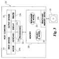
- FIG. 3is a diagrammatic view of a system for performing integrated circuit simulation in accordance with the process of FIG. 1 .
- FIG. 4is a diagrammatic view of a system to perform integrated circuit testing in accordance with the process of FIG. 1 .
- One embodiment of the present inventionis a unique technique to simulate and test integrated circuitry.
- This techniquecan include providing a model of a responder integrated circuit to simulate communications with a model of a project integrated circuit under development, providing the responder integrated circuit and project integrated circuit, and testing the project integrated circuit with the responder integrated circuit.
- Further embodimentsinclude other unique methods, systems, devices, or apparatus.
- FIG. 1diagrammatically depicts Integrated Circuit (IC) development process 20 .
- Stage 22a new project IC is designed.
- the project ICcan be of a complex type, having a high degree of integration.
- Stage 22includes providing a logical model for the project IC design that can be used to test the design through simulation.
- the designis specified by one or more Hardware Description Language (HDL) modules. These modules can be selected from a library to customize the cell array of an Application Specific Integrated Circuit (ASIC).
- ASICApplication Specific Integrated Circuit
- One or more corresponding synthesis toolscan be used to generate a netlist to embody the project IC design in the ASIC.
- U.S. Pat. No. 5,841,663 to Sharma et al.provides an example of this approach.
- some or all modelingis provided with the “C” programming language.
- the logical modeling of the project ICis of different type, and/or is only partially developed using ASIC technology or is developed in a fully customized manner without ASIC technology.
- SoC 120includes one or more processor(s) 122 coupled to a number of communication devices 124 by system bus 126 .
- Communication devices 124include Universal Serial Bus (USB) slave 130 , 12 C (or I 2 C) device 132 , Universal Asynchronous Receiver/Transmitter (UART) 134 , UART InfraRed (UART-IR) 136 , and PCI bus bridge 138 .
- Communication devices 124each have a corresponding communication interface 140 . In other embodiments, more or fewer communication devices 124 are included and/or one or more different types of communication devices 124 are included as would occur to one skilled in the art.
- SoC 120can include other devices such as one or more memories, clocks, caches, to name just a few.
- a responder circuit designis provided. This design is provided to interface with communication devices of the project IC design.
- the responder circuit designcan be specified before, during, or after the project IC design in stage 22 . It is envisioned that for selected project IC designs having a communication device subsystem of a previously developed IC, a previously developed responder circuit design could be utilized. Still, in other embodiments, the responder circuit design can be created as the project IC design is being created or subsequent to a given stage of the project design. In one preferred embodiment, the responder circuit design is in the form of an integrated circuit modeled in the same manner as the project IC design. In one more preferred embodiment, the responder circuit is integrated using one or more HDL modules common to the project IC design. Nonetheless, in still other embodiments, the form and/or modeling of the responder circuit can vary as would occur to one skilled in the art.
- FIG. 2provides one example of a responder circuit design as SoC responder 150 .
- Responder 150includes at least one processor 152 coupled to a number of communication devices 154 by system bus 156 .
- Communication devices 154include Universal Serial Bus (USB) Host 160 , 12 C (or I 2 C) device 162 , Universal Asynchronous Receiver/Transmitter (UART) 164 , UART InfraRed (UART-IR) 166 , and PCI bus bridge 168 each having one of communication interfaces 180 operatively coupled with a corresponding one of communication interfaces 140 of SoC 120 to provide a corresponding number of communication pathways 190 .
- USBUniversal Serial Bus
- UARTUniversal Asynchronous Receiver/Transmitter
- UART-IRUART InfraRed
- PCI bus bridge 168each having one of communication interfaces 180 operatively coupled with a corresponding one of communication interfaces 140 of SoC 120 to provide a corresponding number of communication pathways 190 .
- Such couplingcan
- Communication devices 154also include USB slave 170 and ECP printer 172 that are not coupled to SoC 120 . In other embodiments, more or fewer communication devices 154 are included and/or one or more different types of communication devices 154 are included as would occur to one skilled in the art.
- Responder 150can include other devices such as one or more memories, clocks, caches, to name just a few.
- Process 20proceeds from stages 22 and 24 to stage 26 .
- stage 26the project IC design is simulated with a host computer based on its logical modeling. This simulation includes testing communications with the responder circuit logical model.
- modeling communication devices for the project IC design and responder circuit design with the same codecan typically provide a more accurate simulation relative to the application of different models.
- simulation host computer 220is shown with one or more processor(s) 222 .
- Processor(s) 222can be of any type.
- Computer 220also includes operator input devices 224 and operator output devices 226 operatively coupled to processor(s) 222 .
- Input devices 224include a conventional mouse 224 a and keyboard 224 b , and alternatively or additionally can include a trackball, light pen, voice recognition subsystem, and/or different input device type as would occur to those skilled in the art.
- Output devices 226include a conventional graphic display device 226 a and printer 226 b , and alternatively or additionally can include an aural output system, and/or different output device type as would occur to those skilled in the art. Further, in other embodiments, more or fewer operator input devices 224 or operator output devices 226 may be utilized.
- Computer 220also includes memory 228 operatively coupled to processor(s) 222 .
- Memory 228can be of one or more types, such as solid-state electronic memory, magnetic memory, optical memory, or a combination of these.
- memory 228includes a removable/portable memory device 228 a that is symbolically shown with a removable storage disk 230 .
- Storage disk 230can be an optically-readable disk (such as a CD ROM or DVD) or a magnetically encoded hard disk or floppy disk.
- RMD 228 acan include a magnetically encoded tape or cartridge media, a nonvolatile semiconductor configuration, or a different form of removable memory as would occur to those skilled in the art.
- At least a portion of memory 228is operable to store programming instructions for processor(s) 222 to perform simulation in accordance with stage 26 of process 20 .
- Project IC simulation model 240 and responder circuit model 250are symbolically represented as information stored within memory 228 .
- Computer 220correspondingly executes models 240 and 250 to perform the simulation of stage 26 .
- Letting models 320 and 350represent SoC 120 and responder 150 of FIG. 2, respectively; simulation of stage 26 with computer 220 can be arranged to test communication between respective USB slave 130 and host 160 , I 2 C bus devices 132 and 162 , UART 134 and 164 , UART-IR 136 and 166 , and/or PCI bus bridge 138 and 168 .
- the responder IC logic modeloperates as a slave under the control of the project IC logic model.
- This embodimentincludes a communication testing protocol that is provided through a communication medium operatively coupling the responder IC logic model and the project IC logic model.
- a selectioncan be made with one or more dedicated configuration inputs to the responder circuit logic model.
- configuration input connections 192are illustrated to select among communication pathways 190 . These connections can be provided in the form of general purpose Input/Output (I/O) pins of the responder IC.
- a default mediumcan be used. In those applications where a relatively simple, low overhead communication medium is desired, a UART communication link may be selected; however, in other embodiments with or without a UART link, a different medium or media could be used.
- test protocolfor the project IC model and responder circuit model is provided as follows in Table I:
- the first columnspecifies commands sent by the project IC model and the second column specifies the corresponding function of the responder IC model in response to the first column command.
- a different protocol and/or testing methodologycan be alternatively or additionally utilized.
- one or more general purpose Input/Output (I/O) pinsare used to provide an interrupt protocol to synchronize the project IC and responder circuit models for testing.
- conditional 28tests if the simulated design is acceptable. If not, process 20 loops back to stage 22 and/or stage 24 to make desired design changes.
- process 120proceeds from the affirmative branch of conditional 28 to stages 32 and 34 .
- One or more prototype project ICsare fabricated in stage 32 according to the accepted design.
- a responder ICis provided in stage 34 .
- Stage 34can be executed before, during, or after stage 32 . It is envisioned that a responder IC could be available from an earlier project IC design process that has the same communication device subsystems. In other cases, prototype responder ICs are fabricated.
- Process 20proceeds from stages 32 and 34 to stage 36 to perform testing in a laboratory environment.
- Stage 36includes coupling the project IC and responder IC together to perform communication testing. This testing can generally duplicate testing performed during simulation in stage 26 , including the testing protocol of Table I if desired.
- the responder ICcan be provided in stand-alone laboratory test equipment.
- process 20continues with conditional 38 to determine whether the prototype is acceptable. If the test results are not acceptable, process 20 loops back to stages 22 , 24 , 26 , 32 , 34 , and/or 36 as needed to address the unacceptable results. These options are represented by a dashed line having multiple arrowheads that extends from the negative branch of conditional 38 . If the results are acceptable, then process 20 proceeds to stage 42 to produce the project IC. Stage 46 includes the performance of testing in a production environment with the responder IC. The responder IC is included in production test equipment for stage 46 . As in the case of stage 36 , stage 146 can be executed using the protocol of Table I if desired. Process 20 then halts. When desired, utilizing a responder IC for testing in stages 36 and 46 that corresponds to the responder circuit simulation model used in stage 26 can often provide a development process that is less problematic compared to other approaches.
- Test system 400is illustrated, with like reference numerals representing like features of previously described embodiments.
- Test system 400is representative of an arrangement that can be used to perform the testing of stage 36 and/or stage 46 .
- System 400includes a project IC in the form of SoC 420 .
- SoC 420is engaged to a test bed 425 for the purpose of conducting testing.
- SoC 420is configured with the same devices as SoC 120 , including communication devices 130 operatively coupled to test equipment 440 via communication pathways 490 .
- Test equipment 440includes responder IC 450 in the form of a Responder System-on-Chip (RSoC).
- RSSoCResponder System-on-Chip
- Responder IC 450can be configured the same as responder 150 and correspondingly includes communication devices 160 operatively coupled to SoC 420 via communication pathways 190 .
- Responder IC 450further includes configuration input connections 192 to select a communication media for testing control.
- the testing protocolcan be the same as that described in connection with Table I, through an interrupt synchronization technique, or with a different approach as would occur to one skilled in the art.
- SoC 420includes a general purpose Input/Output (I/O) connection 494 coupled to responder IC 450 .
- I/O connections 494can each be utilized to send a signal to selectively turn of one or more clocks of responder IC 450 (not shown) during simulation or physical testing of other devices and/or circuitry of SoC 420 (such as SoC memory testing, cache integrity validation, etc).
- ICs/modelscan be tested and or simulated with a common responder IC/model. Additionally or alternatively, multiple responder ICs/models could be provided.
- simulationmay not be performed with a model of a responder IC.
- testing with a responder ICmay not be performed in both the laboratory environment and production environment.
- Another embodimentincludes a computer operable to simulate operation of an IC design with a responder IC model.
- a computer-readable devicecarrying instructions executable to perform simulations with a responder circuit model, to conduct testing with a responder IC, or both.
- Another embodimentincludes test equipment with a responder IC including at least some of the features of responder circuit logic models and/or responder ICs previously described.
- Another embodimentis a responder IC device.
Landscapes
- Engineering & Computer Science (AREA)
- General Engineering & Computer Science (AREA)
- Physics & Mathematics (AREA)
- General Physics & Mathematics (AREA)
- Computer Hardware Design (AREA)
- Theoretical Computer Science (AREA)
- Evolutionary Computation (AREA)
- Geometry (AREA)
- Test And Diagnosis Of Digital Computers (AREA)
- Tests Of Electronic Circuits (AREA)
Abstract
Description
| TABLE I | |
| MASTER | |
| COMMAND | SLAVE FUNCTION |
| Reset | Slave responder performs a complete re- |
| initialization. | |
| Select Test | Specifies a test number to be executed and the |
| number of times the test should be executed, | |
| building a Selected Test List. | |
| Run Selected Tests | All tests previously selected by the Select Test |
| command are executed. | |
| Halt All Tests | All test execution is terminated. The Selected |
| Test List is cleared of all entries. | |
| Halt Selected Test | The specified test is terminated and it is |
| removed from the Selected Test List. | |
| Read slave responder | The status of the slave responder is returned. |
| Status | |
| Read Selected Test | The status for the specified test is returned. |
| Status | |
Claims (23)
Priority Applications (5)
| Application Number | Priority Date | Filing Date | Title |
|---|---|---|---|
| US09/997,764US6543034B1 (en) | 2001-11-30 | 2001-11-30 | Multi-environment testing with a responder |
| AU2002365493AAU2002365493A1 (en) | 2001-11-30 | 2002-11-20 | Multi-environment testing with a responder |
| EP02803889AEP1461732A2 (en) | 2001-11-30 | 2002-11-20 | Multi-environment testing with a responder |
| JP2003547978AJP2005510787A (en) | 2001-11-30 | 2002-11-20 | Diverse environmental tests with transponders |
| PCT/IB2002/004906WO2003046591A2 (en) | 2001-11-30 | 2002-11-20 | Multi-environment testing with a responder |
Applications Claiming Priority (1)
| Application Number | Priority Date | Filing Date | Title |
|---|---|---|---|
| US09/997,764US6543034B1 (en) | 2001-11-30 | 2001-11-30 | Multi-environment testing with a responder |
Publications (1)
| Publication Number | Publication Date |
|---|---|
| US6543034B1true US6543034B1 (en) | 2003-04-01 |
Family
ID=25544364
Family Applications (1)
| Application Number | Title | Priority Date | Filing Date |
|---|---|---|---|
| US09/997,764Expired - LifetimeUS6543034B1 (en) | 2001-11-30 | 2001-11-30 | Multi-environment testing with a responder |
Country Status (5)
| Country | Link |
|---|---|
| US (1) | US6543034B1 (en) |
| EP (1) | EP1461732A2 (en) |
| JP (1) | JP2005510787A (en) |
| AU (1) | AU2002365493A1 (en) |
| WO (1) | WO2003046591A2 (en) |
Cited By (7)
| Publication number | Priority date | Publication date | Assignee | Title |
|---|---|---|---|---|
| US20040255070A1 (en)* | 2003-06-12 | 2004-12-16 | Larson Thane M. | Inter-integrated circuit router for supporting independent transmission rates |
| US20100235803A1 (en)* | 2009-03-16 | 2010-09-16 | Lara Gramark | Method and Apparatus for Automatically Connecting Component Interfaces in a Model Description |
| US20140154997A1 (en)* | 2012-11-30 | 2014-06-05 | Mediatek Inc. | Rf testing system |
| US20160197684A1 (en)* | 2011-06-13 | 2016-07-07 | Mediatek Inc. | Rf testing system with serdes device |
| US20160204881A1 (en)* | 2011-06-13 | 2016-07-14 | Mediatek Inc. | Rf testing system using integrated circuit |
| US9525500B2 (en) | 2011-06-13 | 2016-12-20 | Mediatek Inc. | Low-cost test/calibration system and calibrated device for low-cost test/calibration system |
| US10069578B2 (en) | 2011-06-13 | 2018-09-04 | Mediatek Inc. | RF testing system with parallelized processing |
Citations (15)
| Publication number | Priority date | Publication date | Assignee | Title |
|---|---|---|---|---|
| US5487018A (en) | 1993-08-13 | 1996-01-23 | Vlsi Technology, Inc. | Electronic design automation apparatus and method utilizing a physical information database |
| US5546562A (en)* | 1995-02-28 | 1996-08-13 | Patel; Chandresh | Method and apparatus to emulate VLSI circuits within a logic simulator |
| US5559715A (en) | 1992-03-11 | 1996-09-24 | Vlsi Technology, Inc. | Timing model and characterization system for logic simulation of integrated circuits which takes into account process, temperature and power supply variations |
| US5663900A (en)* | 1993-09-10 | 1997-09-02 | Vasona Systems, Inc. | Electronic simulation and emulation system |
| US5692160A (en) | 1994-12-14 | 1997-11-25 | Vlsi Technology, Inc. | Temperature, process and voltage variant slew rate based power usage simulation and method |
| US5726902A (en) | 1995-06-07 | 1998-03-10 | Vlsi Technology, Inc. | Method and apparatus for characterizing timing behavior of datapaths for integrated circuit design and fabrication |
| US5826073A (en)* | 1995-10-06 | 1998-10-20 | Advanced Micro Devices, Inc. | Self-modifying code handling system |
| US5841663A (en) | 1995-09-14 | 1998-11-24 | Vlsi Technology, Inc. | Apparatus and method for synthesizing integrated circuits using parameterized HDL modules |
| US5926629A (en)* | 1997-02-18 | 1999-07-20 | Advanced Micro Devices, Inc. | Continuously operating interconnection bus |
| US6006022A (en) | 1996-11-15 | 1999-12-21 | Microsystem Synthesis, Inc. | Cross-linked development and deployment apparatus and method |
| US6154803A (en)* | 1998-12-18 | 2000-11-28 | Philips Semiconductors, Inc. | Method and arrangement for passing data between a reference chip and an external bus |
| US6195593B1 (en) | 1997-09-03 | 2001-02-27 | Seiko Epson Corporation | Reusable modules for complex integrated circuit devices |
| US6240543B1 (en) | 1998-12-01 | 2001-05-29 | Narpat Bhandari | Integration of manufacturing test of multiple system on a chip without substantial simulation |
| US6269467B1 (en) | 1998-09-30 | 2001-07-31 | Cadence Design Systems, Inc. | Block based design methodology |
| US6286114B1 (en) | 1997-10-27 | 2001-09-04 | Altera Corporation | Enhanced embedded logic analyzer |
- 2001
- 2001-11-30USUS09/997,764patent/US6543034B1/ennot_activeExpired - Lifetime
- 2002
- 2002-11-20AUAU2002365493Apatent/AU2002365493A1/ennot_activeAbandoned
- 2002-11-20WOPCT/IB2002/004906patent/WO2003046591A2/enactiveApplication Filing
- 2002-11-20EPEP02803889Apatent/EP1461732A2/ennot_activeWithdrawn
- 2002-11-20JPJP2003547978Apatent/JP2005510787A/enactivePending
Patent Citations (15)
| Publication number | Priority date | Publication date | Assignee | Title |
|---|---|---|---|---|
| US5559715A (en) | 1992-03-11 | 1996-09-24 | Vlsi Technology, Inc. | Timing model and characterization system for logic simulation of integrated circuits which takes into account process, temperature and power supply variations |
| US5487018A (en) | 1993-08-13 | 1996-01-23 | Vlsi Technology, Inc. | Electronic design automation apparatus and method utilizing a physical information database |
| US5663900A (en)* | 1993-09-10 | 1997-09-02 | Vasona Systems, Inc. | Electronic simulation and emulation system |
| US5692160A (en) | 1994-12-14 | 1997-11-25 | Vlsi Technology, Inc. | Temperature, process and voltage variant slew rate based power usage simulation and method |
| US5546562A (en)* | 1995-02-28 | 1996-08-13 | Patel; Chandresh | Method and apparatus to emulate VLSI circuits within a logic simulator |
| US5726902A (en) | 1995-06-07 | 1998-03-10 | Vlsi Technology, Inc. | Method and apparatus for characterizing timing behavior of datapaths for integrated circuit design and fabrication |
| US5841663A (en) | 1995-09-14 | 1998-11-24 | Vlsi Technology, Inc. | Apparatus and method for synthesizing integrated circuits using parameterized HDL modules |
| US5826073A (en)* | 1995-10-06 | 1998-10-20 | Advanced Micro Devices, Inc. | Self-modifying code handling system |
| US6006022A (en) | 1996-11-15 | 1999-12-21 | Microsystem Synthesis, Inc. | Cross-linked development and deployment apparatus and method |
| US5926629A (en)* | 1997-02-18 | 1999-07-20 | Advanced Micro Devices, Inc. | Continuously operating interconnection bus |
| US6195593B1 (en) | 1997-09-03 | 2001-02-27 | Seiko Epson Corporation | Reusable modules for complex integrated circuit devices |
| US6286114B1 (en) | 1997-10-27 | 2001-09-04 | Altera Corporation | Enhanced embedded logic analyzer |
| US6269467B1 (en) | 1998-09-30 | 2001-07-31 | Cadence Design Systems, Inc. | Block based design methodology |
| US6240543B1 (en) | 1998-12-01 | 2001-05-29 | Narpat Bhandari | Integration of manufacturing test of multiple system on a chip without substantial simulation |
| US6154803A (en)* | 1998-12-18 | 2000-11-28 | Philips Semiconductors, Inc. | Method and arrangement for passing data between a reference chip and an external bus |
Cited By (10)
| Publication number | Priority date | Publication date | Assignee | Title |
|---|---|---|---|---|
| US20040255070A1 (en)* | 2003-06-12 | 2004-12-16 | Larson Thane M. | Inter-integrated circuit router for supporting independent transmission rates |
| US20100235803A1 (en)* | 2009-03-16 | 2010-09-16 | Lara Gramark | Method and Apparatus for Automatically Connecting Component Interfaces in a Model Description |
| US20150229415A1 (en)* | 2011-06-13 | 2015-08-13 | Mediatek Inc. | Rf testing system |
| US20160197684A1 (en)* | 2011-06-13 | 2016-07-07 | Mediatek Inc. | Rf testing system with serdes device |
| US20160204881A1 (en)* | 2011-06-13 | 2016-07-14 | Mediatek Inc. | Rf testing system using integrated circuit |
| US9525500B2 (en) | 2011-06-13 | 2016-12-20 | Mediatek Inc. | Low-cost test/calibration system and calibrated device for low-cost test/calibration system |
| US10069578B2 (en) | 2011-06-13 | 2018-09-04 | Mediatek Inc. | RF testing system with parallelized processing |
| US10110325B2 (en)* | 2011-06-13 | 2018-10-23 | Mediatek Inc. | RF testing system |
| US10320494B2 (en)* | 2011-06-13 | 2019-06-11 | Mediatek Inc. | RF testing system using integrated circuit |
| US20140154997A1 (en)* | 2012-11-30 | 2014-06-05 | Mediatek Inc. | Rf testing system |
Also Published As
| Publication number | Publication date |
|---|---|
| WO2003046591A3 (en) | 2004-06-03 |
| AU2002365493A8 (en) | 2003-06-10 |
| AU2002365493A1 (en) | 2003-06-10 |
| WO2003046591A2 (en) | 2003-06-05 |
| EP1461732A2 (en) | 2004-09-29 |
| JP2005510787A (en) | 2005-04-21 |
Similar Documents
| Publication | Publication Date | Title |
|---|---|---|
| US8234617B2 (en) | Method and system for re-using digital assertions in a mixed signal design | |
| US7711536B2 (en) | System and method for verification aware synthesis | |
| JP4806529B2 (en) | Debugging methods and systems that use replicated logic | |
| US6353915B1 (en) | Methods for evaluating systems of electronic components | |
| US7561999B2 (en) | Verification apparatus, verification method, and program | |
| US8650513B2 (en) | Reducing x-pessimism in gate-level simulation and verification | |
| CN107784185B (en) | Method and device for extracting pseudo path in gate-level netlist and terminal equipment | |
| US12073159B2 (en) | Computing device and method for detecting clock domain crossing violation in design of memory device | |
| US20020108094A1 (en) | System and method for designing integrated circuits | |
| US8504347B2 (en) | Simulation apparatus, simulation method, and program to perform simulation on design data of a target circuit | |
| US6543034B1 (en) | Multi-environment testing with a responder | |
| CN115470125B (en) | Log file-based debugging method, device and storage medium | |
| US8321825B2 (en) | Method and system for synthesizing relative timing constraints on an integrated circuit design to facilitate timing verification | |
| US20050246673A1 (en) | Method and system for performing static timing analysis on digital electronic circuits | |
| US7657851B2 (en) | Device, system, and method for correction of integrated circuit design | |
| JP2005510787A5 (en) | ||
| CN1815480B (en) | Method and system for generating hardware design language triggers from oscillograms | |
| US6813751B2 (en) | Creating standard VHDL test environments | |
| US7086017B1 (en) | Method of post-implementation simulation of a HDL design | |
| WO2003023658A2 (en) | Emulation system and method | |
| US8775987B1 (en) | Generation of a replay module for simulation of a circuit design | |
| US7865345B2 (en) | Simulation apparatus and method | |
| CN115983171B (en) | Method and simulation platform for post-simulation of system on chip | |
| Rajsuman | Extending EDA environment from design to test | |
| US8205186B1 (en) | Incremental modification of instrumentation logic |
Legal Events
| Date | Code | Title | Description |
|---|---|---|---|
| AS | Assignment | Owner name:KONINKLIJKE PHILIPS ELECTRONICS N.V., NETHERLANDS Free format text:ASSIGNMENT OF ASSIGNORS INTEREST;ASSIGNORS:GOFF, LONNIE C.;LOGSDON, BRIAN D.;PETRYK, EDWARD M.;REEL/FRAME:012340/0529 Effective date:20011129 | |
| STCF | Information on status: patent grant | Free format text:PATENTED CASE | |
| FPAY | Fee payment | Year of fee payment:4 | |
| AS | Assignment | Owner name:NXP B.V., NETHERLANDS Free format text:ASSIGNMENT OF ASSIGNORS INTEREST;ASSIGNOR:KONINKLIJKE PHILIPS ELECTRONICS N.V.;REEL/FRAME:018635/0787 Effective date:20061117 | |
| FPAY | Fee payment | Year of fee payment:8 | |
| FPAY | Fee payment | Year of fee payment:12 | |
| AS | Assignment | Owner name:PHILIPS SEMICONDUCTORS INTERNATIONAL B.V., NETHERL Free format text:ASSIGNMENT OF ASSIGNORS INTEREST;ASSIGNOR:KONINKLIJKE PHILIPS ELECTRONICS N.V.;REEL/FRAME:043955/0001 Effective date:20060928 Owner name:NXP B.V., NETHERLANDS Free format text:CHANGE OF NAME;ASSIGNOR:PHILIPS SEMICONDUCTORS INTERNATIONAL B.V.;REEL/FRAME:043951/0436 Effective date:20060929 |