US6542983B1 - Microcomputer/floating point processor interface and method - Google Patents
Microcomputer/floating point processor interface and methodDownload PDFInfo
- Publication number
- US6542983B1 US6542983B1US09/410,925US41092599AUS6542983B1US 6542983 B1US6542983 B1US 6542983B1US 41092599 AUS41092599 AUS 41092599AUS 6542983 B1US6542983 B1US 6542983B1
- Authority
- US
- United States
- Prior art keywords
- fpu
- cpu
- pipestage
- pipeline
- instruction
- Prior art date
- Legal status (The legal status is an assumption and is not a legal conclusion. Google has not performed a legal analysis and makes no representation as to the accuracy of the status listed.)
- Expired - Lifetime
Links
Images


Classifications
- G—PHYSICS
- G06—COMPUTING OR CALCULATING; COUNTING
- G06F—ELECTRIC DIGITAL DATA PROCESSING
- G06F9/00—Arrangements for program control, e.g. control units
- G06F9/06—Arrangements for program control, e.g. control units using stored programs, i.e. using an internal store of processing equipment to receive or retain programs
- G06F9/30—Arrangements for executing machine instructions, e.g. instruction decode
- G06F9/38—Concurrent instruction execution, e.g. pipeline or look ahead
- G06F9/3867—Concurrent instruction execution, e.g. pipeline or look ahead using instruction pipelines
- G06F9/3875—Pipelining a single stage, e.g. superpipelining
- G—PHYSICS
- G06—COMPUTING OR CALCULATING; COUNTING
- G06F—ELECTRIC DIGITAL DATA PROCESSING
- G06F9/00—Arrangements for program control, e.g. control units
- G06F9/06—Arrangements for program control, e.g. control units using stored programs, i.e. using an internal store of processing equipment to receive or retain programs
- G06F9/30—Arrangements for executing machine instructions, e.g. instruction decode
- G06F9/38—Concurrent instruction execution, e.g. pipeline or look ahead
- G06F9/3867—Concurrent instruction execution, e.g. pipeline or look ahead using instruction pipelines
- G—PHYSICS
- G06—COMPUTING OR CALCULATING; COUNTING
- G06F—ELECTRIC DIGITAL DATA PROCESSING
- G06F9/00—Arrangements for program control, e.g. control units
- G06F9/06—Arrangements for program control, e.g. control units using stored programs, i.e. using an internal store of processing equipment to receive or retain programs
- G06F9/30—Arrangements for executing machine instructions, e.g. instruction decode
- G06F9/38—Concurrent instruction execution, e.g. pipeline or look ahead
- G06F9/3877—Concurrent instruction execution, e.g. pipeline or look ahead using a slave processor, e.g. coprocessor
Definitions
- the present inventionrelates generally to microcomputers. More particularly, the present invention relates to a single chip microcomputer having a central processing execution unit and a floating point execution unit.
- SOCsSystem-on-chip devices
- microcomputersare well-known. These devices generally include a processor (CPU), one or more modules, bus interfaces, memory devices, and one or more system busses for communicating information.
- processorsCPU
- modulesOne module that may be incorporated into a microcomputer is a floating point coprocessor, typically referred to as a floating point unit or FPU.
- a floating point unitis used to execute instructions that involve non-integer numbers.
- non-integer numbersare represented as a computer word divided into two parts, an exponent and a significant.
- Floating point unitsare special purpose processors designed specifically to execute arithmetic operations involving these non-integer representations of numbers.
- Microcomputers with fully integrated or embedded floating point unitsare known.
- the floating point unitWhen the floating point unit is embedded in, or tightly integrated with the CPU of the microcomputer, the FPU and CPU typically share a number of operational blocks. Therefore, the interface between the FPU and CPU, both in hardware and software, is very tightly integrated.
- this level of integrationtypically provides high performance, such as high throughput, it can be difficult to design and build versions of the microcomputer without the FPU for sale to customers who do not want or do not require the functions of the FPU. Removing the FPU from the microcomputer can be quite difficult as a number of aspects of the microcomputer design have to be changed and in some cases removing the FPU from the microcomputer can involve a significant redesign effort.
- microcomputer and floating point processor systemsare also known.
- the microcomputer and floating point unitare typically separate integrated circuit chips and an interface is provided for the exchange of instructions and data between the CPU and the FPU.
- One form of interface between the CPU and the FPUuses a buffering arrangement.
- the timing and synchronization requirements for execution of instructions in the CPU and FPUcan be relaxed, resulting in relatively “loose” coupling between the processors.
- This type of systemhas advantages in that it is straightforward to offer the FPU as an option to the microcomputer.
- performance, such as throughputmay suffer because operation of the CPU and FPU is not tightly synchronized.
- a single chip microcomputerincluding a central processing unit (CPU), a memory unit coupled to the CPU, an interface adapted to couple the CPU to a floating point instruction processing unit (FPU), an FPU present signal coupled from the interface to the CPU, floating point present signal having a first state that indicates to the CPU that an FPU is present in the single chip microcomputer and a second state that indicates to the CPU that an FPU is not present in the single chip microcomputer, where the single chip microcomputer responds to the first state of the FPU present signal to send floating point instructions across the interface to the FPU and to the second state of the signal to trap floating point instructions.
- CPUcentral processing unit
- FPUfloating point instruction processing unit
- FPU present signalcoupled from the interface to the CPU
- floating point present signalhaving a first state that indicates to the CPU that an FPU is present in the single chip microcomputer and a second state that indicates to the CPU that an FPU is not present in the single chip microcomputer
- the single chip microcomputerraises an exception when the FPU present signal is in the second state and a floating point instruction is trapped.
- the computer systemcomprises a single chip microcomputer, including a central processing unit, a memory unit coupled to the CPU, an interface adapted to couple the CPU to a floating point instruction processing unit (FPU), means for indicating to the CPU that and FPU is present in the single chip microcomputer, and means, responsive to the means for indicating, for controlling the single chip microcomputer in response to the means for indicating.
- a single chip microcomputerincluding a central processing unit, a memory unit coupled to the CPU, an interface adapted to couple the CPU to a floating point instruction processing unit (FPU), means for indicating to the CPU that and FPU is present in the single chip microcomputer, and means, responsive to the means for indicating, for controlling the single chip microcomputer in response to the means for indicating.
- FPUfloating point instruction processing unit
- the computer systemincludes means for indicating comprises an FPU present signal having a first state that indicates that an FPU is present in the single chip microcomputer and a second state that indicates that an FPU is not present in the single chip microcomputer.
- the computer systemincludes means for controlling sends floating point instructions to the FPU when the FPU present signal is in the first state and traps floating point instructions when the FPU present signal is in the second state.
- the computer systemcomprises a single chip microcomputer including a central processing unit (CPU), a memory unit coupled to the central processing unit, an interface adapted to couple the CPU to a floating point instruction processing unit (FPU), a method of determining if an FPU is present in the computer system, the method comprises the steps of using the FPU to send an FPU present signal across the interface to the CPU where the FPU present signal has a first state indicating to the CPU that an FPU is present in the single chip microcomputer and a second state indicating to the CPU that an FPU is not present in the single chip microcomputer; and using the CPU to respond to the FPU present signal so that the single chip microcomputer sends floating point instructions across the interface to the FPU in response to the first state of the FPU present signal an traps floating point instructions in response to the second state of the FPU present signal.
- CPUcentral processing unit
- FPUfloating point instruction processing unit
- the computer systemincludes a central processing unit (CPU) execution pipeline and a floating point unit (FPU) execution pipeline, the CPU execution pipeline including a CPU decoder pipestage and the FPU execution pipeline including an FPU decoder pipestage
- the methodcomprises the steps of a) sending a first instruction to the CPU decoder pipestage, b) sending the first instruction to the FPU decoder pipestage, c) generating a signal indicating that the first instruction has been accepted by the CPU decoder pipestage, d) generating a signal indicating that the first instruction has been accepted by the FPU decoder pipestage, e) sending a second instruction to the CPU decoder pipestage in response to step d, and f) sending a second instruction to the FPU decoder pipestage in response to step c.
- CPUcentral processing unit
- FPUfloating point unit
- the computer systemfurther comprises the step of resending the first instruction to the CPU decoder pipestage until the signal in step d is generated.
- the computerfurther comprises the step of resending the first instruction to the FPU decoder pipestage until the signal in step c is generated
- the computer systemincludes a central processing unit (CPU) execution pipeline and a floating point unit (FPU) execution pipeline, the CPU pipeline including a plurality of pipestages and the FPU pipeline including a plurality of pipestages, where each CPU pipestage in the CPU pipeline has a corresponding pipestage in the FPU pipeline, a Method of synchronizing operation of the CPU pipeline and the FPU pipeline, the method comprises the steps of, a) receiving an instruction in a first CPU pipestage, b) receiving the instruction in a corresponding first FPU pipestage, c) processing the instruction in the first CPU pipestage, d) processing the instruction in the first FPU pipestage, e) generating, by the first CPU pipestage, a first signal indicating that the instruction has been processed by first CPU pipestage and is ready to proceed to a second pipestage in the CPU pipeline, f) generating by the first FPU pipestage, a second signal indicating that the instruction has been processed by the first FPU pipestage and is ready to proceed to a second
- the second pipestage in the CPU pipelinefurther responds to the second signal to prevent the second pipestage in the CPU pipeline from sending instructions to the third pipestage in the CPU pipeline until another second signal is received from the first FPU pipestage.
- the FPU pipelinefurther responds to the first signal to prevent the second pipestage in the FPU pipeline from sending instructions to the third pipestage in the FPU pipeline until another first signal is received from the first CPU pipestage.
- the computercomprises a central processing unit (CPU) execution pipeline including a plurality of pipestages, a floating point unit (FPU) execution pipeline including a plurality of pipestages, where each CPU pipestage in the CPU pipeline has a corresponding pipestage in the FPU pipeline, first means for controlling transmission of instructions from a first CPU pipestage to a second CPU pipestage in response to a control signal provided by an FPU pipestage, and second means for controlling transmission of instructions from a first FPU pipestage to a second FPU pipestage in response to a control signal provided by a CPU pipestage.
- CPUcentral processing unit
- FPUfloating point unit
- the first means for controllingis a token signal having a first state that enables transmission of instructions and a second state that disables transmission of instructions.
- the first CPU pipestageresponds to the first state of the token signal to transmit an instruction.
- the first CPU pipestagegenerates a signal that cancels the token signal when an instruction is transmitted.
- the first FPU pipestageresponds to the first state of the token signal to transmit an instruction.
- the first FPU pipestagegenerates a signal that cancels the token signal when an instruction is transmitted.
- the computerincludes a central processing unit (CPU) execution pipeline and a floating point unit (FPU) execution pipeline, the CPU pipeline including a plurality of pipestages and the FPU pipeline including a plurality of pipestages where each CPU pipestage has a corresponding pipestage in the FPU pipeline, a method of synchronizing operation of the CPU pipeline and the FPU pipeline, the method comprises the steps of a) providing instructions to each pipestage in the CPU pipeline, b) providing the instructions to each corresponding pipestage in the FPU pipeline, c) executing the instructions in the CPU pipeline, d) executing the instructions in the FPU pipeline, e) stalling the CPU pipeline in response to a stall condition, f) stalling the FPU unit pipeline a predetermined number of pipestages after the CPU pipeline has stalled, g) storing the state of execution of the floating point processing unit pipeline in response to step f, h) removing the stall condition and restarting the CPU pipeline, I) presenting the data stored in step
- CPUcentral processing unit
- step (g)further comprises storing execution results of each pipestage in the FPU pipeline.
- the predetermined number of pipestagescomprises one pipestage.
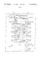
- FIG. 1is a microcomputer according to the invention including an optional floating point processor (FPU);
- FPUfloating point processor
- FIG. 2is a block diagram illustrating a floating point unit and the interface between the FPU and the CPU that may be used in the microcomputer of FIG. 1;
- FIG. 3is a diagram illustrating the CPU execution pipeline and the FPU execution pipeline and the relationship between the pipe stages in each pipeline of the microcomputer of FIG. 1;
- FIG. 4is a logical block diagram of the interface between the CPU and the FPU in the microcomputer of FIG. 1 illustrating the circuitry and signals used to synchronize the two pipelines;
- FIG. 5is a more detailed logical block diagram of the CPU predecoder stage instruction buffering mechanism of FIG. 4;
- FIG. 6is a more detailed logical block diagram of the decoder/E 1 -F 1 stage synchronization logic of FIG. 4;
- FIG. 7is a logical block diagram of a portion of FIG. 4 illustrating the load/store unit E stage stall and resynchronization logic.
- FIG. 1illustrates a single chip microcomputer 50 according to the invention.
- Microcomputer 50includes a central processing unit core 51 for executing operations within the computer.
- An integer central processing unit (CPU) 52 and an optional floating point processor unit (FPU) 54are provided as part of the CPU core 51 .
- An interface 56which will be explained in more detail hereinafter, provides the mechanism for exchanging data, instructions, and control signals between integer CPU 52 and FPU 54 .
- CPU core 51also includes other modules such as, for example, an instruction fetch unit and a load store unite.
- CPU 52refers to the portion of CPU core 51 that executes integer operations.
- CPU core 51is coupled to a system bus 58 via a data link 60 .
- System bus 58provides a pathway for the exchange of data, instructions, and control signals among the modules and interfaces attached to the system bus.
- a RAM interface 62 that provides an interface to off-chip random access memoryis coupled to system bus 58 via data link 64 .
- a ROM interface 66 that provides access to off-chip read only memoryis coupled to system bus 58 via data link 68 .
- Other system bus modules 70are coupled to system bus 58 by data link 72 .
- a debug module 74 containing a debug interfaceis coupled to system bus 58 via data link 76 .
- Debug module 74receives debugging data from CPU core 51 via data link 80 .
- Debug module 74provides an off-chip interface via debug link 82 that allows microcomputer 50 to interface to external equipment or software.
- Microcomputer 50also includes a system bus arbiter 84 coupled to system bus 58 via data link 86 .
- System bus arbiter 84controls the flow of data traffic over system bus 58 .
- System bus 84sends debugging information, such as the triggering of system bus watchpoints via data link 88 to debug module 74 .
- Microcomputer 50also includes a peripheral component bus 90 .
- a peripheral component bus arbiter 92controls the data flow over the peripheral component bus 90 , is coupled to peripheral component bus 90 via data link 94 , and provides an interface to system bus 58 via data link 96 .
- Peripheral component bus modules 98can be coupled to peripheral component bus 90 via data link 100 .
- a peripheral component bus interface 102coupled to peripheral component bus 90 via data link 104 provides an interface for off-chip components to peripheral component bus 90 .
- FIG. 2is a more detailed block diagram of FPU 54 and interface 56 illustrated in FIG. 1 .
- FPU 54includes a number of functional modules.
- Module 110is a floating point unit decoder and pipe control block that decodes 32 bit instructions from CPU 52 sent via interface 56 .
- Module 112is a floating point unit register file and forwarding network.
- Module 114comprising execution pipestages F 1 , F 2 , F 3 and F 4 respectively numbered as 116 , 118 , 120 and 122 is a floating point logical execution module for executing coexecuted CPU instructions and for controlling register access.
- Module 124comprising execution pipestages F 1 , F 2 , F 3 , F 4 , F 5 respectively numbered as 126 , 128 , 130 , 132 and 134 is a floating point vector and basic compute unit for executing compute, blocking computer, vector compute, blocking vector compute, type conversion, and polynomial compute operations.
- Module 136comprising execution pipestages FDS 1 and FDS 2 respectively numbered as 138 and 140 is a floating point divide and square root executing unit for executing non-blocking compute operations such as divide and square root operations.
- Completion busses 142 and dispatch busses 144couple modules 114 , 124 , and 136 to module 112 .
- a feature of the inventionis that the FPU 54 is designed to be a self-contained, detachable portion of the CPU core 51 . Therefore, data movement between CPU 52 and FPU 54 via interface 56 is limited to 32 bit instructions 150 and two 64 bit busses 152 and 154 for transporting data.
- a control signal interface 156is also provided for controlling and synchronizing execution of instructions between CPU 52 and FPU 54 .
- FIG. 3illustrates the structures of the execution pipelines and the relationship between the various pipestages of the execution pipelines in CPU 52 and FPU 54 .
- CPU 52includes an execution pipeline 160 .
- FPU 54includes an execution pipeline 162 .
- Each pipeline 160 and 162include a number of pipestages.
- CPU 52 and FPU 54share the instruction fetch pipestage 164 and the pre-decode pipestage 166 .
- CPU pipeline 160includes a decode pipestage 168 , three execution pipestages 170 , 172 and 174 , and a writeback pipestage 176 .
- FPU pipeline 162includes a floating point decode pipestage 178 , five execution pipestages 126 , 128 , 130 , 132 and 134 , and a floating point writeback stage 180 that sends the results of the floating point unit execution pipeline 162 to module 112 for transmission back to CPU 52 .
- a first category of instructionsis a pure CPU instruction that executes totally in CPU pipeline 160 and does not require any contribution for completion from FPU pipeline 162 .
- CPU pipeline 160 and FPU pipeline 162are closely coupled and, therefore, when a pure CPU instruction is executing in CPU pipeline 160 an instruction image is executing in FPU pipeline 162 .
- the image of that instruction in FPU pipeline 162is a bubble.
- a second category of instructions that executes in CPU pipeline 160 and FPU pipeline 162is FPU instructions. All FPU instructions are in this group. Every FPU instruction must execute to some degree in CPU pipeline 160 as an instruction image, if only to gather exception details and completion status.
- a first subgroup of FPU instructionsare joint CPU-FPU instructions with data exchange. These instructions involve data exchange between CPU pipeline 160 and FPU pipeline 162 , either from the FPU to the CPU or from the CPU to the FPU.
- a second subgroup of FPU instructionsare joint CPU-FPU instructions without data exchange. These instructions execute entirely within the FPU pipeline and CPU pipeline 160 is only involved with these instructions to gather exception information and completion status.
- a floating point placeholderexecutes through the CPU pipeline 160 as the instruction image gathering exception details and keeping the pipelines synchronized.
- the FPU instructionis also executing in CPU pipeline 160 as the instruction image so the pipelines remain synchronized.
- a feature of the inventionis to maintain a close coupling and synchronization of execution between FPU pipeline 162 and CPU pipeline 160 . Maintaining a close coupling and synchronization between the two pipelines has several advantages.
- a significant advantageis that maintaining close synchronization between FPU pipeline 162 and CPU pipeline 160 allows microcomputer 150 to maintain a precise exception model.
- a precise exception modelmeans that instructions must execute and finish in order so that when an exception is generated due to some hardware or software problem in microcomputer 50 , the state of execution of microcomputer 50 will be clear at the time the error occurred. This allows the state of various components at the time the exception occurred to be examined and corrective action taken. If a precise exception model is not maintained, then when an error occurs it can become difficult to determine the state that various components of the microcomputer were in at the time the error occurred, which can make tracing and correction of the problem very difficult.
- FPU 54can be optional. As will be explained in more detail hereinafter, the interface 56 between FPU 54 and CPU 52 is designed so that deleting FPU from the particular version of microcomputer 50 does not require significant redesign of the microcomputer. FPU 54 can simply be completely deleted from the single integrated circuit containing microcomputer 50 without redesigning the circuitry or modifying the software.
- interface 56allows FPU 54 to be an option in microcomputer 50 but also provides a higher level of throughput performance then separate microcomputers and coprocessors would, while at the same time allowing microcomputer 50 to maintain a precise exception model of operation.
- FIG. 4is a more detailed block diagram illustrating the interface 56 between CPU 52 and FPU 54 .
- Table 1sets forth the set of signals used for communication between CPU 52 and FPU 54 .
- Column “Name”provides a name of each control signal.
- Column “Dir”indicates the direction of each signal with respect to whether the signal is input to the FPU or output from the FPU.
- Column “Src”indicates which unit, as between the CPG, (clock generator circuit), the FPU, the instruction fetch unit (IFU) the load/store unit (LSU) is the source of the signal.
- Column “Size”indicates the number of bits in the signal.
- Column “Stage Sent”indicates which stage in CPU 52 or CPU 54 sends the signal.
- Column “Latch by”indicates whether the signal is latched on the CPU side of interface 56 or on the FPU side of interface 56 .
- Column “Description”provides a description of each signal.
- the signal fpu_presentindicates to the CPU whether an FPU is present or not. If an FPU is present, this signal will be asserted and the CPU will recognize that the FPU is available. Under these circumstances, the CPU will send instructions to the FPU. If the signal fpu_present is de-asserted, the CPU will recognize that there is no FPU. Under these circumstances, if an FPU instruction is encountered, the CPU will trap on the instructions and raise an exception. Thus, the only signal that changes depending on the presence or absence of an FPU is the fpu_present signal.
- the floating point disable signal ifu_sr_fdis provided to disable FPU 54 .
- this flagis set in the status register (SR) of the CPU, FPU 54 is disabled and all floating point instructions are trapped.
- FIG. 4illustrates the circuitry and signals to synchronize CPU pipeline 160 and FPU pipeline 162 .
- CPU pipeline 160 and FPU pipeline 162normally execute instructions in lockstep, with execution of an instruction proceeding through a respective pair of CPU and FPU pipe stages, for example, 126 , 170 or 128 , 172 , simultaneously.
- there are three points in the pipelineswhere they can slip out of the synchronization and need to be resynchronized before execution can continue.
- the maximum slippage between the pipelinesis limited to one instruction or one pipestage in the illustrated embodiment.
- Each pipestage 168 , 170 , 172 , 174 , 176 in CPU pipeline 160has a respective buffer 224 , 170 A, 172 A, 174 A and 176 A for storing computational results from a prior pipestage.
- Each pipestage 178 , 126 , 128 , 130 , 132 , 134 , 180 in FPU pipeline 162has a respective buffer 226 , 126 A, 128 A, 130 A, 132 A, 134 A, 180 A for storing computational results from a prior pipestage.
- latchesare provided on the CPU side for signals arriving from the FPU and on the FPU side for signals arriving from the CPU.
- the CPU sideincludes latches 170 B, 172 B, 174 B and 174 C.
- the FPU sideincludes latches 126 B and 284 .
- FIGS. 4-7allows the CPU and FPU pipelines to be up to one pipestage out of synchronization with each other.
- the inventionis not limited to a one pipestage slip but could be any predetermined number of pipestages (or even a zero pipestage slip). That is, the pipelines could be allowed to be out of synchronization by a predetermined number of clock cycles before the pipelines are stalled, as long as the data and state of execution of each pipeline is stored so that when the pipelines are restarted, the data from any pipestage in one pipeline is made available to the other pipeline with the proper timing so that the pipelines can be resynchronized to their same relationship prior to stalling without any loss of data. Allowing the CPU and FPU pipelines to be out of synchronization by a predetermined number of clock cycles also compensates for the time of flight between the CPU pipeline and the FPU pipeline across interface 56 .
- FIG. 5figure illustrates operation of the CPU predecoder stage instruction buffering mechanism.
- This section of the circuitryincludes a predecode logic circuit 200 that receives an instruction fetch unit decoder stall signal from the CPU instruction fetch unit via latch 202 .
- Predecoder logic 200also receives a floating point unit decoder stall signal from the floating point unit decoder 178 via latch 204 .
- Fpu_dc_stallis a signal generated whenever floating point unit decoder 178 can not receive and latch the next instruction being sent out by the shared predecode stage. Ifu_dec_stall is a signal generated whenever the instruction fetch unit of CPU 52 is stalled for any reason.
- a multiplexer 206has a number of inputs coupled to predecode buffer 208 .
- Connection 210allows the output of multiplexer 206 to be sent to predecode buffer 208 , predecoder 212 or multiplexer 214 .
- the output of predecoder 212is sent, via connection 216 to multiplexer 218 .
- Multiplexers 214 and 218have respective outputs 220 , 222 which are respectively coupled to instruction fetch unit decode buffer 224 and FPU decode buffer 226 .
- Buffers 224 and 226serve to hold instructions being decoded by the decoders 168 and 178 .
- Buffer 224has an output 227 that allows the instruction in buffer 224 to be recirculated back to multiplexer 218 .
- buffer 226has an output 228 that allows the current instruction in buffer 226 to be recirculated back to multiplexer 214 . If the signal ifu_dec_stall is asserted for any reason, multiplexer 218 will keep selecting and recirculating the instruction until the stall condition is removed. In a like manner, if the fpu_dec_stall signal is asserted, multiplexer 214 will keep recirculating instruction 228 into buffer 226 until the stall condition is removed.
- predecode logic 200performs the following functions:
- IFU _taken⁇ ifu _dec_stall — q
- FPU _taken⁇ fpu _dec_stall — q
- IFU _taken_earlier — dIFU _taken & ⁇ new — PD _inst_valid
- IFU_/FPU_taken_earlier_qare the latched versions of the IFU_/FPU_taken_earlier_d signals.
- predecode stage instructionis always stored in predecode buffer 208 for an additional clock cycle. This ensures that the content of predecode buffer 208 is always available in the predecode stage until both CPU pipeline decoder 168 and FPU pipeline decoder 178 have accepted the same instruction.
- decoder stages 168 and 178will be no more than one instruction of synchronization and the same instruction will exit CPU decoder stage 168 and FPU decoder stage 178 at the same time and thus both pipelines will be synchronized at this point.
- FIG. 6figure illustrates a logical block diagram of the CPU decoder/FPU decoder-E 1 /F 1 synchronization logic.
- a “go-token” passing mechanismis used to resynchronize the pipelines before the two images of the same floating point instruction leave respective pipestages 170 , 126 .
- Each pipelinesends a go-token to the other pipeline when it decodes a valid floating point instruction and is not stalled due to any decoder stage stalling condition.
- the go-tokenis then latched in the other pipeline and used as a gating condition for the image of that same instruction in the other pipeline to proceed beyond pipestages 170 , 126 .
- ifu_fp_go_decis a go-token signal from CPU decoder pipestage 166 that indicates that the instruction in decoder pipestage 166 has been successfully decoded and that the decoder pipestage is not stalled.
- the signal fpu_fp_go_decis a token signal from floating point unit decoder pipestage 178 that indicates that the floating point instruction in decoder pipestage 178 has been successfully decoded and there are no decoder pipestage stalling conditions. Since these token signals are generated after decoding has been completed, they arrive in the other pipeline relatively late in the clock cycle. As a result, they are latched immediately in the receiving pipeline pipestage.
- Combinatorial logic 244responds to the signal latched in latch 244 to generate the signal ifp_fp_may_leave_e 1 on line 246 that triggers execution pipestage 170 to send the instruction on to pipestage 172 .
- a signal ifu_fp_leaving_e 1is generated on line 247 which resets combinatorial logic 244 to deactivate the ifu_fp_may_leave_e 1 signal so that the next instruction loaded into pipestage 170 will require another fpu_fp_go_dec token before it can exit pipestage 170 .
- the signal ifu_fp_go_f 1is output by latch 240 into combinatorial logic 248 .
- Combinatorial logic 248generates a signal fpu_fp_may_leave_f 1 on line 250 that triggers pipestage 126 of the FPU to send the instruction on to pipestage 128 .
- pipestage 126Once the instruction leaves pipestage 126 , pipestage 126 generates an fpu_fp_leave_f 1 signal on line 252 that causes combinatorial logic 248 to deactivate signal fpu_fp_may_leave_f 1 so that the next instruction loaded into pipestage 126 will require another ifu_fp_go_dec token signal before that instruction can leave pipestage 126 .
- a go-tokenwill always be signaled to the pipeline 162 as long as no decode pipestage stalling condition is detected on a valid floating point instruction in decoder pipestage 168 .
- fpu — fp _may_leave — f 1ifu — fp _go_dec — q
- fpu _token_received — dfpu — fp _may_leave — f 1 & ⁇ fpu — fp _leaving — f 1
- FIG. 7illustrates logic circuitry that is used to stall and resychronize the CPU pipeline 160 and FPU pipeline 162 under these conditions.
- logic 280 illustrated in FIG. 7is used to resynchronize the two pipelines.
- the signal lsu_stall_e 3is asserted on line 282 .
- this signalis asserted, pipestage 174 and all prior pipestages 166 , 170 , and 172 of the CPU pipeline 162 are immediately stalled.
- the lsu_stall_e 3 signal on line 282is also sent across interface 56 to logic 280 .
- the signal lsu_stall_e 3is latched into latch 284 during the clock cycle in which the signal stalls the CPU pipeline 160 . However, during the clock cycle in which lsu_stall_e 3 is asserted, the FPU pipeline 162 continues execution.
- the latched stall signalis sent to pipestage 132 of FPU pipeline 162 which immediately stalls FPU pipestage 178 , 126 , 128 , 130 , and 132 .
- the stalling signal on line 286 from latch 284is used to disable latching of latches 288 , 290 , and 292 and to control multiplexers 294 , 296 , and 298 to select the latched data on lines 301 , 303 , and 305 , respectively so as to maintain the status of the go_token from decoder pipestage FCMP (an FPU instruction that compares two floating point registers) and exception information from execution pipestage 128 .
- FCMPan FPU instruction that compares two floating point registers
- Latching of data from the FPU execution units that communicate with execution pipestages in CPU pipeline 160assures that this data is not lost when FPU pipeline 162 is stalled. This ensures that the data being sent to CPU pipeline 160 on lines 295 , 297 , and 299 is the data from the FPU pipestages that was produced during the clock cycle in which the FPU pipeline execution advanced with respect to the CPU pipeline execution.
- the floating point unitadvances by one pipestage with respect to the CPU pipeline, but the FPU pipeline is stalled at the next clock cycle and all data that would normally have been transmitted to the CPU pipeline is instead stored.
- CPU pipeline 160When the lsu-stall_e 3 signal on line 282 is deactivated, CPU pipeline 160 immediately begins execution and advances by one pipestage with respect to the now-stalled FPU pipeline 162 . During this clock cycle, the CPU pipestages read the data on lines 295 , 297 , and 299 from latches 288 , 290 and 292 , respectively with had been stored when the FPU was stalled. As a result of latch 284 , on the next clock cycle, the stall signal on lines 285 and 286 is deactivated. This causes FPU pipeline 162 to restart immediately.
- a final synchronization point between CPU pipeline 160 and FPU pipeline 162occurs when an instruction enters the writeback pipestage 176 of CPU pipeline 160 and when an instruction enters pipestage 132 of FPU pipeline 162 .
- cancel instructions from the CPU to the FPUare sent as an ifu_fpu_cancel_wb signal on line 306 . If the instruction has not been canceled by the CPU at pipestage 176 , floating point pipeline 160 continues execution.
- FPU pipeline 162receives a cancel instruction, FPU 54 cancels all instructions executing in FPU pipestages 178 , 126 , 128 , 130 , and 132 .
- the FPU 54while being only an option in CPU core 51 , is able to be interfaced to CPU 52 so that the CPU and FPU are closely coupled to maintain high performance throughput.
- the close coupling of the CPU pipeline and FPU pipelinesince they are constrained to slip with respect to each other by a predetermined number of cycles, maintains a precise exception model in microcomputer 50 .
- the present inventionmay be implemented in a single integrated circuit.
Landscapes
- Engineering & Computer Science (AREA)
- Software Systems (AREA)
- Theoretical Computer Science (AREA)
- Physics & Mathematics (AREA)
- General Engineering & Computer Science (AREA)
- General Physics & Mathematics (AREA)
- Advance Control (AREA)
- Microcomputers (AREA)
Abstract
Description
| Stage | ||||||
| Name | Dir | Src | Size | Sent | Latched by | Description |
| cpg_fpu_clk_cn | in | 1 | Clock stop for the FPU | |||
| fpu_present | out | 1 | CPU | Indicates if FPU is present or not | ||
| ifu_sr_fd | in | IFU | 1 | W | CPU | The SR Floating-point Disable bit. |
| ifu_fpu_inst_pd | in | IFU | 28 | PD | FPU | Opcode (sent in pre-decode stage) |
| ifu_fpu_inst_valid_pd | in | 1 | PD | FPU | Opcode is valid (in pre-decode stage) | |
| usable in FPD | ||||||
| ifu_fpu_pred_inst_pd | in | IFU | I | PD | FPU | The instruction being sent is on a |
| branch prediction path. | ||||||
| ifu_fp_go_dec | in | IFU | 1 | D | FPU | The valid FP instruction in the IFU |
| decode stage can proceed (no stalling) | ||||||
| ifu_fpu_mispred_c2 | in | 1 | E2 | CPU | A mispredicted cond branch is resolved | |
| in the CPU pipe. | ||||||
| ifu_fpu_cancel_wb | in | IFU | 1 | W | CPU | An FPU/CPU instruction in WB has an |
| associated CPU exception and the | ||||||
| pipeline must be canceled (from F4 | ||||||
| back to FPD). | ||||||
| Isu_stall_e3 | in | 1 | E3 | FPU | E3 stage back is stalled in CPU (only | |
| usable in F4) | ||||||
| ifu_fpu_data_wb[63:0] | in | IFU | 64 | W | CPU | Data from Integer CPU for FLD, |
| FMOV (usable in F4) | ||||||
| fpu_fp_go_dec | out | 1 | FPD | CPU | The valid FP instruction in the FPU | |
| decode stage can proceed | ||||||
| fpu_dec_stall | out | 1 | FPD | CPU | FPU decode buffer has a valid FP | |
| instruction and FPD is stalled | ||||||
| internally, and therefore can not accept | ||||||
| a new instruction from CPU. | ||||||
| fpu_ifu_excep_f2 | out | 1 | F2 | CPU | FPU exception has occurred | |
| fpu_lsu_data_f1[63:0] | out | 64 | F1 | CPU | Data to Integer CPU (usable in E2) | |
| fpu_lsu_fcmp_f2 | out | 1 | F2 | CPU | FCMP result (used in E3) | |
Claims (3)
Priority Applications (2)
| Application Number | Priority Date | Filing Date | Title |
|---|---|---|---|
| US09/410,925US6542983B1 (en) | 1999-10-01 | 1999-10-01 | Microcomputer/floating point processor interface and method |
| JP2000292744AJP2001147810A (en) | 1999-10-01 | 2000-09-26 | Microcomputer / floating point processor interface and method |
Applications Claiming Priority (1)
| Application Number | Priority Date | Filing Date | Title |
|---|---|---|---|
| US09/410,925US6542983B1 (en) | 1999-10-01 | 1999-10-01 | Microcomputer/floating point processor interface and method |
Publications (1)
| Publication Number | Publication Date |
|---|---|
| US6542983B1true US6542983B1 (en) | 2003-04-01 |
Family
ID=23626817
Family Applications (1)
| Application Number | Title | Priority Date | Filing Date |
|---|---|---|---|
| US09/410,925Expired - LifetimeUS6542983B1 (en) | 1999-10-01 | 1999-10-01 | Microcomputer/floating point processor interface and method |
Country Status (2)
| Country | Link |
|---|---|
| US (1) | US6542983B1 (en) |
| JP (1) | JP2001147810A (en) |
Cited By (4)
| Publication number | Priority date | Publication date | Assignee | Title |
|---|---|---|---|---|
| US20040236896A1 (en)* | 2000-01-31 | 2004-11-25 | Ruban Kanapathippillai | Memory with memory clusters for power reduction in an integrated circuit |
| US20050232218A1 (en)* | 2004-04-19 | 2005-10-20 | Broadcom Corporation | Low-power operation of systems requiring low-latency and high-throughput |
| US20100115245A1 (en)* | 2008-10-30 | 2010-05-06 | Atsuya Okazaki | Detecting and recovering from timing violations of a processor |
| US7788470B1 (en)* | 2008-03-27 | 2010-08-31 | Xilinx, Inc. | Shadow pipeline in an auxiliary processor unit controller |
Families Citing this family (1)
| Publication number | Priority date | Publication date | Assignee | Title |
|---|---|---|---|---|
| JP5555514B2 (en)* | 2010-03-17 | 2014-07-23 | ルネサスエレクトロニクス株式会社 | Processor system |
Citations (75)
| Publication number | Priority date | Publication date | Assignee | Title |
|---|---|---|---|---|
| EP0165660A1 (en) | 1984-05-18 | 1985-12-27 | Unisys Corporation | Passbook printer |
| EP0165600A2 (en) | 1984-06-20 | 1985-12-27 | Convex Computer Corporation | Input/output bus for computer |
| US4814981A (en) | 1986-09-18 | 1989-03-21 | Digital Equipment Corporation | Cache invalidate protocol for digital data processing system |
| US5197130A (en)* | 1989-12-29 | 1993-03-23 | Supercomputer Systems Limited Partnership | Cluster architecture for a highly parallel scalar/vector multiprocessor system |
| US5251311A (en) | 1989-10-12 | 1993-10-05 | Nec Corporation | Method and apparatus for processing information and providing cache invalidation information |
| US5386565A (en) | 1990-01-23 | 1995-01-31 | Hitachi, Ltd. | Method and system for controlling/monitoring computer system having plural operating systems to run thereon |
| EP0636976A1 (en) | 1993-07-28 | 1995-02-01 | Koninklijke Philips Electronics N.V. | Microcontroller provided with hardware for supporting debugging as based on boundary scan standard-type extensions |
| EP0652516A1 (en) | 1993-11-03 | 1995-05-10 | Advanced Micro Devices, Inc. | Integrated microprocessor |
| US5423050A (en) | 1991-11-27 | 1995-06-06 | Ncr Corporation | Intermodule test across system bus utilizing serial test bus |
| US5428756A (en)* | 1989-09-25 | 1995-06-27 | Matsushita Electric Industrial Co., Ltd. | Pipelined computer with control of instruction advance |
| US5434804A (en) | 1993-12-29 | 1995-07-18 | Intel Corporation | Method and apparatus for synchronizing a JTAG test control signal to an on-chip clock signal |
| US5440705A (en) | 1986-03-04 | 1995-08-08 | Advanced Micro Devices, Inc. | Address modulo adjust unit for a memory management unit for monolithic digital signal processor |
| US5448576A (en) | 1992-10-29 | 1995-09-05 | Bull Hn Information Systems Inc. | Boundary scan architecture extension |
| US5452432A (en) | 1990-08-14 | 1995-09-19 | Chips And Technologies, Inc. | Partially resettable, segmented DMA counter |
| US5455936A (en) | 1993-04-28 | 1995-10-03 | Nec Corporation | Debugger operable with only background monitor |
| US5479652A (en) | 1992-04-27 | 1995-12-26 | Intel Corporation | Microprocessor with an external command mode for diagnosis and debugging |
| US5483518A (en) | 1992-06-17 | 1996-01-09 | Texas Instruments Incorporated | Addressable shadow port and protocol for serial bus networks |
| US5488688A (en) | 1994-03-30 | 1996-01-30 | Motorola, Inc. | Data processor with real-time diagnostic capability |
| EP0702239A2 (en) | 1994-09-01 | 1996-03-20 | STMicroelectronics Limited | A controller for implementing scan testing |
| US5530965A (en) | 1992-11-06 | 1996-06-25 | Hitachi, Ltd. | Multiply connectable microprocessor and microprocessor system |
| EP0720092A1 (en) | 1994-12-28 | 1996-07-03 | Hewlett-Packard Company | Microprocessor with debugging system |
| US5570375A (en) | 1995-05-10 | 1996-10-29 | National Science Council Of R.O.C. | IEEE Std. 1149.1 boundary scan circuit capable of built-in self-testing |
| JPH08320796A (en) | 1994-09-09 | 1996-12-03 | Hitachi Ltd | Data processing device |
| JPH08329687A (en) | 1995-06-05 | 1996-12-13 | Hitachi Ltd | Semiconductor integrated circuit |
| US5596734A (en) | 1993-12-17 | 1997-01-21 | Intel Corporation | Method and apparatus for programming embedded memories of a variety of integrated circuits using the IEEE test access port |
| US5598551A (en) | 1993-07-16 | 1997-01-28 | Unisys Corporation | Cache invalidation sequence system utilizing odd and even invalidation queues with shorter invalidation cycles |
| US5608881A (en) | 1992-11-06 | 1997-03-04 | Hitachi, Ltd. | Microcomputer system for accessing hierarchical buses |
| US5613153A (en) | 1994-10-03 | 1997-03-18 | International Business Machines Corporation | Coherency and synchronization mechanisms for I/O channel controllers in a data processing system |
| US5627842A (en) | 1993-01-21 | 1997-05-06 | Digital Equipment Corporation | Architecture for system-wide standardized intra-module and inter-module fault testing |
| US5657273A (en) | 1994-11-22 | 1997-08-12 | Hitachi, Ltd. | Semiconductor device capable of concurrently transferring data over read paths and write paths to a memory cell array |
| JPH09212358A (en) | 1996-01-31 | 1997-08-15 | Hitachi Ltd | Data processing device and microprocessor |
| US5682545A (en) | 1991-06-24 | 1997-10-28 | Hitachi, Ltd. | Microcomputer having 16 bit fixed length instruction format |
| JPH09311786A (en) | 1996-03-18 | 1997-12-02 | Hitachi Ltd | Data processing device |
| US5704034A (en) | 1995-08-30 | 1997-12-30 | Motorola, Inc. | Method and circuit for initializing a data processing system |
| US5708773A (en) | 1995-07-20 | 1998-01-13 | Unisys Corporation | JTAG interface system for communicating with compliant and non-compliant JTAG devices |
| US5724549A (en) | 1992-04-06 | 1998-03-03 | Cyrix Corporation | Cache coherency without bus master arbitration signals |
| WO1998013759A1 (en) | 1996-09-27 | 1998-04-02 | Hitachi, Ltd. | Data processor and data processing system |
| US5737516A (en) | 1995-08-30 | 1998-04-07 | Motorola, Inc. | Data processing system for performing a debug function and method therefor |
| JPH10106269A (en) | 1996-08-06 | 1998-04-24 | Hitachi Ltd | Semiconductor storage device, semiconductor device, data processing device, and computer system |
| US5751621A (en) | 1994-11-17 | 1998-05-12 | Hitachi, Ltd. | Multiply-add unit and data processing apparatus using it |
| JPH10124484A (en) | 1996-10-16 | 1998-05-15 | Hitachi Ltd | Data processor and data processing system |
| US5768152A (en) | 1996-08-28 | 1998-06-16 | International Business Machines Corp. | Performance monitoring through JTAG 1149.1 interface |
| US5771240A (en) | 1996-11-14 | 1998-06-23 | Hewlett-Packard Company | Test systems for obtaining a sample-on-the-fly event trace for an integrated circuit with an integrated debug trigger apparatus and an external pulse pin |
| US5774701A (en) | 1995-07-10 | 1998-06-30 | Hitachi, Ltd. | Microprocessor operating at high and low clok frequencies |
| JPH10177520A (en) | 1996-10-16 | 1998-06-30 | Hitachi Ltd | Data processor and data processing system |
| US5778237A (en) | 1995-01-10 | 1998-07-07 | Hitachi, Ltd. | Data processor and single-chip microcomputer with changing clock frequency and operating voltage |
| US5781558A (en) | 1996-08-14 | 1998-07-14 | International Computers Limited | Diagnostic memory access |
| US5796978A (en) | 1994-09-09 | 1998-08-18 | Hitachi, Ltd. | Data processor having an address translation buffer operable with variable page sizes |
| US5828825A (en) | 1993-12-22 | 1998-10-27 | Intel Corporation | Method and apparatus for pseudo-direct access to embedded memories of a micro-controller integrated circuit via the IEEE test access port |
| US5832248A (en) | 1992-11-06 | 1998-11-03 | Hitachi, Ltd. | Semiconductor integrated circuit having CPU and multiplier |
| US5835963A (en) | 1994-09-09 | 1998-11-10 | Hitachi, Ltd. | Processor with an addressable address translation buffer operative in associative and non-associative modes |
| US5848247A (en) | 1994-09-13 | 1998-12-08 | Hitachi, Ltd. | Microprocessor having PC card interface |
| US5860000A (en)* | 1996-01-31 | 1999-01-12 | Hitachi Micro Systems, Inc. | Floating point unit pipeline synchronized with processor pipeline |
| US5860127A (en) | 1995-06-01 | 1999-01-12 | Hitachi, Ltd. | Cache memory employing dynamically controlled data array start timing and a microcomputer using the same |
| US5862387A (en) | 1995-04-21 | 1999-01-19 | Intel Corporation | Method and apparatus for handling bus master and direct memory access (DMA) requests at an I/O controller |
| US5867726A (en) | 1995-05-02 | 1999-02-02 | Hitachi, Ltd. | Microcomputer |
| US5884057A (en)* | 1994-01-11 | 1999-03-16 | Exponential Technology, Inc. | Temporal re-alignment of a floating point pipeline to an integer pipeline for emulation of a load-operate architecture on a load/store processor |
| US5884092A (en) | 1995-10-09 | 1999-03-16 | Hitachi, Ltd. | System for maintaining fixed-point data alignment within a combination CPU and DSP system |
| US5896550A (en) | 1997-04-03 | 1999-04-20 | Vlsi Technology, Inc. | Direct memory access controller with full read/write capability |
| US5918045A (en) | 1996-10-18 | 1999-06-29 | Hitachi, Ltd. | Data processor and data processing system |
| US5930523A (en) | 1993-09-17 | 1999-07-27 | Hitachi Ltd. | Microcomputer having multiple bus structure coupling CPU to other processing elements |
| US5930833A (en) | 1994-04-19 | 1999-07-27 | Hitachi, Ltd. | Logical cache memory storing logical and physical address information for resolving synonym problems |
| EP0933926A1 (en) | 1998-01-30 | 1999-08-04 | STMicroelectronics Limited | DMA controller |
| US5944841A (en) | 1997-04-15 | 1999-08-31 | Advanced Micro Devices, Inc. | Microprocessor with built-in instruction tracing capability |
| US5950012A (en) | 1996-03-08 | 1999-09-07 | Texas Instruments Incorporated | Single chip microprocessor circuits, systems, and methods for self-loading patch micro-operation codes and patch microinstruction codes |
| US5953538A (en) | 1996-11-12 | 1999-09-14 | Digital Equipment Corporation | Method and apparatus providing DMA transfers between devices coupled to different host bus bridges |
| US5956477A (en) | 1996-11-25 | 1999-09-21 | Hewlett-Packard Company | Method for processing information in a microprocessor to facilitate debug and performance monitoring |
| EP0945805A1 (en) | 1998-03-23 | 1999-09-29 | STMicroelectronics Limited | A cache coherency mechanism |
| US5978902A (en) | 1997-04-08 | 1999-11-02 | Advanced Micro Devices, Inc. | Debug interface including operating system access of a serial/parallel debug port |
| US5978874A (en) | 1996-07-01 | 1999-11-02 | Sun Microsystems, Inc. | Implementing snooping on a split-transaction computer system bus |
| US5983379A (en) | 1996-10-31 | 1999-11-09 | Sgs-Thomson Microelectronics Limited | Test access port controller and a method of effecting communication using the same |
| US5983017A (en) | 1996-11-12 | 1999-11-09 | Lsi Logic Corporation | Virtual monitor debugging method and apparatus |
| EP0959411A1 (en) | 1998-04-29 | 1999-11-24 | STMicroelectronics Limited | Packet distribution in a microcomputer |
| US6044456A (en)* | 1998-01-05 | 2000-03-28 | Intel Corporation | Electronic system and method for maintaining synchronization of multiple front-end pipelines |
| US6385719B1 (en)* | 1999-06-30 | 2002-05-07 | International Business Machines Corporation | Method and apparatus for synchronizing parallel pipelines in a superscalar microprocessor |
- 1999
- 1999-10-01USUS09/410,925patent/US6542983B1/ennot_activeExpired - Lifetime
- 2000
- 2000-09-26JPJP2000292744Apatent/JP2001147810A/enactivePending
Patent Citations (77)
| Publication number | Priority date | Publication date | Assignee | Title |
|---|---|---|---|---|
| EP0165660A1 (en) | 1984-05-18 | 1985-12-27 | Unisys Corporation | Passbook printer |
| EP0165600A2 (en) | 1984-06-20 | 1985-12-27 | Convex Computer Corporation | Input/output bus for computer |
| US5440705A (en) | 1986-03-04 | 1995-08-08 | Advanced Micro Devices, Inc. | Address modulo adjust unit for a memory management unit for monolithic digital signal processor |
| US4814981A (en) | 1986-09-18 | 1989-03-21 | Digital Equipment Corporation | Cache invalidate protocol for digital data processing system |
| US5428756A (en)* | 1989-09-25 | 1995-06-27 | Matsushita Electric Industrial Co., Ltd. | Pipelined computer with control of instruction advance |
| US5251311A (en) | 1989-10-12 | 1993-10-05 | Nec Corporation | Method and apparatus for processing information and providing cache invalidation information |
| US5197130A (en)* | 1989-12-29 | 1993-03-23 | Supercomputer Systems Limited Partnership | Cluster architecture for a highly parallel scalar/vector multiprocessor system |
| US5386565A (en) | 1990-01-23 | 1995-01-31 | Hitachi, Ltd. | Method and system for controlling/monitoring computer system having plural operating systems to run thereon |
| US5452432A (en) | 1990-08-14 | 1995-09-19 | Chips And Technologies, Inc. | Partially resettable, segmented DMA counter |
| US5682545A (en) | 1991-06-24 | 1997-10-28 | Hitachi, Ltd. | Microcomputer having 16 bit fixed length instruction format |
| US5423050A (en) | 1991-11-27 | 1995-06-06 | Ncr Corporation | Intermodule test across system bus utilizing serial test bus |
| US5724549A (en) | 1992-04-06 | 1998-03-03 | Cyrix Corporation | Cache coherency without bus master arbitration signals |
| US5479652B1 (en) | 1992-04-27 | 2000-05-02 | Intel Corp | Microprocessor with an external command mode for diagnosis and debugging |
| US5479652A (en) | 1992-04-27 | 1995-12-26 | Intel Corporation | Microprocessor with an external command mode for diagnosis and debugging |
| US5483518A (en) | 1992-06-17 | 1996-01-09 | Texas Instruments Incorporated | Addressable shadow port and protocol for serial bus networks |
| US5448576A (en) | 1992-10-29 | 1995-09-05 | Bull Hn Information Systems Inc. | Boundary scan architecture extension |
| US5832248A (en) | 1992-11-06 | 1998-11-03 | Hitachi, Ltd. | Semiconductor integrated circuit having CPU and multiplier |
| US5608881A (en) | 1992-11-06 | 1997-03-04 | Hitachi, Ltd. | Microcomputer system for accessing hierarchical buses |
| US5530965A (en) | 1992-11-06 | 1996-06-25 | Hitachi, Ltd. | Multiply connectable microprocessor and microprocessor system |
| US5627842A (en) | 1993-01-21 | 1997-05-06 | Digital Equipment Corporation | Architecture for system-wide standardized intra-module and inter-module fault testing |
| US5455936A (en) | 1993-04-28 | 1995-10-03 | Nec Corporation | Debugger operable with only background monitor |
| US5598551A (en) | 1993-07-16 | 1997-01-28 | Unisys Corporation | Cache invalidation sequence system utilizing odd and even invalidation queues with shorter invalidation cycles |
| US5590354A (en) | 1993-07-28 | 1996-12-31 | U.S. Philips Corporation | Microcontroller provided with hardware for supporting debugging as based on boundary scan standard-type extensions |
| EP0636976A1 (en) | 1993-07-28 | 1995-02-01 | Koninklijke Philips Electronics N.V. | Microcontroller provided with hardware for supporting debugging as based on boundary scan standard-type extensions |
| US5930523A (en) | 1993-09-17 | 1999-07-27 | Hitachi Ltd. | Microcomputer having multiple bus structure coupling CPU to other processing elements |
| EP0652516A1 (en) | 1993-11-03 | 1995-05-10 | Advanced Micro Devices, Inc. | Integrated microprocessor |
| US5596734A (en) | 1993-12-17 | 1997-01-21 | Intel Corporation | Method and apparatus for programming embedded memories of a variety of integrated circuits using the IEEE test access port |
| US5828825A (en) | 1993-12-22 | 1998-10-27 | Intel Corporation | Method and apparatus for pseudo-direct access to embedded memories of a micro-controller integrated circuit via the IEEE test access port |
| US5434804A (en) | 1993-12-29 | 1995-07-18 | Intel Corporation | Method and apparatus for synchronizing a JTAG test control signal to an on-chip clock signal |
| US5884057A (en)* | 1994-01-11 | 1999-03-16 | Exponential Technology, Inc. | Temporal re-alignment of a floating point pipeline to an integer pipeline for emulation of a load-operate architecture on a load/store processor |
| US5488688A (en) | 1994-03-30 | 1996-01-30 | Motorola, Inc. | Data processor with real-time diagnostic capability |
| US5930833A (en) | 1994-04-19 | 1999-07-27 | Hitachi, Ltd. | Logical cache memory storing logical and physical address information for resolving synonym problems |
| EP0702239A2 (en) | 1994-09-01 | 1996-03-20 | STMicroelectronics Limited | A controller for implementing scan testing |
| JPH08320796A (en) | 1994-09-09 | 1996-12-03 | Hitachi Ltd | Data processing device |
| US5796978A (en) | 1994-09-09 | 1998-08-18 | Hitachi, Ltd. | Data processor having an address translation buffer operable with variable page sizes |
| US5835963A (en) | 1994-09-09 | 1998-11-10 | Hitachi, Ltd. | Processor with an addressable address translation buffer operative in associative and non-associative modes |
| US5848247A (en) | 1994-09-13 | 1998-12-08 | Hitachi, Ltd. | Microprocessor having PC card interface |
| US5613153A (en) | 1994-10-03 | 1997-03-18 | International Business Machines Corporation | Coherency and synchronization mechanisms for I/O channel controllers in a data processing system |
| US5751621A (en) | 1994-11-17 | 1998-05-12 | Hitachi, Ltd. | Multiply-add unit and data processing apparatus using it |
| US5657273A (en) | 1994-11-22 | 1997-08-12 | Hitachi, Ltd. | Semiconductor device capable of concurrently transferring data over read paths and write paths to a memory cell array |
| EP0720092A1 (en) | 1994-12-28 | 1996-07-03 | Hewlett-Packard Company | Microprocessor with debugging system |
| US5778237A (en) | 1995-01-10 | 1998-07-07 | Hitachi, Ltd. | Data processor and single-chip microcomputer with changing clock frequency and operating voltage |
| US5862387A (en) | 1995-04-21 | 1999-01-19 | Intel Corporation | Method and apparatus for handling bus master and direct memory access (DMA) requests at an I/O controller |
| US5867726A (en) | 1995-05-02 | 1999-02-02 | Hitachi, Ltd. | Microcomputer |
| US5570375A (en) | 1995-05-10 | 1996-10-29 | National Science Council Of R.O.C. | IEEE Std. 1149.1 boundary scan circuit capable of built-in self-testing |
| US5860127A (en) | 1995-06-01 | 1999-01-12 | Hitachi, Ltd. | Cache memory employing dynamically controlled data array start timing and a microcomputer using the same |
| JPH08329687A (en) | 1995-06-05 | 1996-12-13 | Hitachi Ltd | Semiconductor integrated circuit |
| US5774701A (en) | 1995-07-10 | 1998-06-30 | Hitachi, Ltd. | Microprocessor operating at high and low clok frequencies |
| US5708773A (en) | 1995-07-20 | 1998-01-13 | Unisys Corporation | JTAG interface system for communicating with compliant and non-compliant JTAG devices |
| US5704034A (en) | 1995-08-30 | 1997-12-30 | Motorola, Inc. | Method and circuit for initializing a data processing system |
| US5737516A (en) | 1995-08-30 | 1998-04-07 | Motorola, Inc. | Data processing system for performing a debug function and method therefor |
| US5884092A (en) | 1995-10-09 | 1999-03-16 | Hitachi, Ltd. | System for maintaining fixed-point data alignment within a combination CPU and DSP system |
| US5860000A (en)* | 1996-01-31 | 1999-01-12 | Hitachi Micro Systems, Inc. | Floating point unit pipeline synchronized with processor pipeline |
| JPH09212358A (en) | 1996-01-31 | 1997-08-15 | Hitachi Ltd | Data processing device and microprocessor |
| US5950012A (en) | 1996-03-08 | 1999-09-07 | Texas Instruments Incorporated | Single chip microprocessor circuits, systems, and methods for self-loading patch micro-operation codes and patch microinstruction codes |
| JPH09311786A (en) | 1996-03-18 | 1997-12-02 | Hitachi Ltd | Data processing device |
| US5978874A (en) | 1996-07-01 | 1999-11-02 | Sun Microsystems, Inc. | Implementing snooping on a split-transaction computer system bus |
| JPH10106269A (en) | 1996-08-06 | 1998-04-24 | Hitachi Ltd | Semiconductor storage device, semiconductor device, data processing device, and computer system |
| US5781558A (en) | 1996-08-14 | 1998-07-14 | International Computers Limited | Diagnostic memory access |
| US5768152A (en) | 1996-08-28 | 1998-06-16 | International Business Machines Corp. | Performance monitoring through JTAG 1149.1 interface |
| WO1998013759A1 (en) | 1996-09-27 | 1998-04-02 | Hitachi, Ltd. | Data processor and data processing system |
| JPH10124484A (en) | 1996-10-16 | 1998-05-15 | Hitachi Ltd | Data processor and data processing system |
| JPH10177520A (en) | 1996-10-16 | 1998-06-30 | Hitachi Ltd | Data processor and data processing system |
| US5918045A (en) | 1996-10-18 | 1999-06-29 | Hitachi, Ltd. | Data processor and data processing system |
| US5983379A (en) | 1996-10-31 | 1999-11-09 | Sgs-Thomson Microelectronics Limited | Test access port controller and a method of effecting communication using the same |
| US5953538A (en) | 1996-11-12 | 1999-09-14 | Digital Equipment Corporation | Method and apparatus providing DMA transfers between devices coupled to different host bus bridges |
| US5983017A (en) | 1996-11-12 | 1999-11-09 | Lsi Logic Corporation | Virtual monitor debugging method and apparatus |
| US5771240A (en) | 1996-11-14 | 1998-06-23 | Hewlett-Packard Company | Test systems for obtaining a sample-on-the-fly event trace for an integrated circuit with an integrated debug trigger apparatus and an external pulse pin |
| US5956477A (en) | 1996-11-25 | 1999-09-21 | Hewlett-Packard Company | Method for processing information in a microprocessor to facilitate debug and performance monitoring |
| US5896550A (en) | 1997-04-03 | 1999-04-20 | Vlsi Technology, Inc. | Direct memory access controller with full read/write capability |
| US5978902A (en) | 1997-04-08 | 1999-11-02 | Advanced Micro Devices, Inc. | Debug interface including operating system access of a serial/parallel debug port |
| US5944841A (en) | 1997-04-15 | 1999-08-31 | Advanced Micro Devices, Inc. | Microprocessor with built-in instruction tracing capability |
| US6044456A (en)* | 1998-01-05 | 2000-03-28 | Intel Corporation | Electronic system and method for maintaining synchronization of multiple front-end pipelines |
| EP0933926A1 (en) | 1998-01-30 | 1999-08-04 | STMicroelectronics Limited | DMA controller |
| EP0945805A1 (en) | 1998-03-23 | 1999-09-29 | STMicroelectronics Limited | A cache coherency mechanism |
| EP0959411A1 (en) | 1998-04-29 | 1999-11-24 | STMicroelectronics Limited | Packet distribution in a microcomputer |
| US6385719B1 (en)* | 1999-06-30 | 2002-05-07 | International Business Machines Corporation | Method and apparatus for synchronizing parallel pipelines in a superscalar microprocessor |
Non-Patent Citations (1)
| Title |
|---|
| York, Richard et al. "Real Time Debug for System-on-Chip Devices", Jun., 1999. |
Cited By (8)
| Publication number | Priority date | Publication date | Assignee | Title |
|---|---|---|---|---|
| US20040236896A1 (en)* | 2000-01-31 | 2004-11-25 | Ruban Kanapathippillai | Memory with memory clusters for power reduction in an integrated circuit |
| US20050076194A1 (en)* | 2000-01-31 | 2005-04-07 | Ruban Kanapathippillai | Unified instruction pipeline for power reduction in a digital signal processor integrated circuit |
| US7233166B2 (en) | 2000-01-31 | 2007-06-19 | Intel Corporation | Bus state keepers |
| US7287148B2 (en)* | 2000-01-31 | 2007-10-23 | Intel Corporation | Unified shared pipeline allowing deactivation of RISC/DSP units for power saving |
| US7318115B2 (en) | 2000-01-31 | 2008-01-08 | Intel Corporation | IC memory complex with controller for clusters of memory blocks I/O multiplexed using collar logic |
| US20050232218A1 (en)* | 2004-04-19 | 2005-10-20 | Broadcom Corporation | Low-power operation of systems requiring low-latency and high-throughput |
| US7788470B1 (en)* | 2008-03-27 | 2010-08-31 | Xilinx, Inc. | Shadow pipeline in an auxiliary processor unit controller |
| US20100115245A1 (en)* | 2008-10-30 | 2010-05-06 | Atsuya Okazaki | Detecting and recovering from timing violations of a processor |
Also Published As
| Publication number | Publication date |
|---|---|
| JP2001147810A (en) | 2001-05-29 |
Similar Documents
| Publication | Publication Date | Title |
|---|---|---|
| EP1050808B1 (en) | Computer instruction scheduling | |
| US11275590B2 (en) | Device and processing architecture for resolving execution pipeline dependencies without requiring no operation instructions in the instruction memory | |
| JP2966892B2 (en) | Digital processing apparatus and method for compiling serial instruction code | |
| US6216223B1 (en) | Methods and apparatus to dynamically reconfigure the instruction pipeline of an indirect very long instruction word scalable processor | |
| EP1535144B3 (en) | Synchronisation between pipelines in a data processing apparatus | |
| US6289445B2 (en) | Circuit and method for initiating exception routines using implicit exception checking | |
| US6301655B1 (en) | Exception processing in asynchronous processor | |
| US7577874B2 (en) | Interactive debug system for multiprocessor array | |
| US20040044883A1 (en) | MFENCE and LFENCE micro-architectural implementation method and system | |
| US5745724A (en) | Scan chain for rapidly identifying first or second objects of selected types in a sequential list | |
| US20090106533A1 (en) | Data processing apparatus | |
| US6859873B2 (en) | Variable length instruction pipeline | |
| US7124224B2 (en) | Method and apparatus for shared resource management in a multiprocessing system | |
| US6594753B2 (en) | Method and apparatus for dual issue of program instructions to symmetric multifunctional execution units | |
| US6542983B1 (en) | Microcomputer/floating point processor interface and method | |
| US6477638B1 (en) | Synchronized instruction advancement through CPU and FPU pipelines | |
| US7216252B1 (en) | Method and apparatus for machine check abort handling in a multiprocessing system | |
| US20020035677A1 (en) | Method and apparatus for pre-processing instructions for a processor | |
| JPH0232424A (en) | Instruction processor | |
| US20020161985A1 (en) | Microcomputer/floating point processor interface and method for synchronization of cpu and fpu pipelines | |
| US20060184775A1 (en) | Computer system with debug facility for debugging a processor capable of predicated execution | |
| US20050125695A1 (en) | Non-inline transaction error correction | |
| US7111152B1 (en) | Computer system that operates in VLIW and superscalar modes and has selectable dependency control | |
| US7783871B2 (en) | Method to remove stale branch predictions for an instruction prior to execution within a microprocessor | |
| US5832253A (en) | Multiprocessors system for selectively wire-oring a combination of signal lines and thereafter using one line to control the running or stalling of a selected processor |
Legal Events
| Date | Code | Title | Description |
|---|---|---|---|
| AS | Assignment | Owner name:HITACHI, LTD., JAPAN Free format text:ASSIGNMENT OF ASSIGNORS INTEREST;ASSIGNORS:GEARTY, MARGARET;PENG, CHIH-JUI;REEL/FRAME:010611/0834;SIGNING DATES FROM 20000210 TO 20000225 | |
| STCF | Information on status: patent grant | Free format text:PATENTED CASE | |
| AS | Assignment | Owner name:RENESAS TECHNOLOGY CORPORATION, JAPAN Free format text:ASSIGNMENT OF ASSIGNORS INTEREST;ASSIGNOR:HITACHI, LTD.;REEL/FRAME:014620/0720 Effective date:20030912 | |
| FEPP | Fee payment procedure | Free format text:PAYOR NUMBER ASSIGNED (ORIGINAL EVENT CODE: ASPN); ENTITY STATUS OF PATENT OWNER: LARGE ENTITY | |
| FEPP | Fee payment procedure | Free format text:PAYER NUMBER DE-ASSIGNED (ORIGINAL EVENT CODE: RMPN); ENTITY STATUS OF PATENT OWNER: LARGE ENTITY Free format text:PAYOR NUMBER ASSIGNED (ORIGINAL EVENT CODE: ASPN); ENTITY STATUS OF PATENT OWNER: LARGE ENTITY | |
| FPAY | Fee payment | Year of fee payment:4 | |
| AS | Assignment | Owner name:RENESAS ELECTRONICS CORPORATION,JAPAN Free format text:CHANGE OF NAME;ASSIGNOR:RENESAS TECHNOLOGY CORPORATION;REEL/FRAME:024588/0306 Effective date:20100401 Owner name:RENESAS ELECTRONICS CORPORATION, JAPAN Free format text:CHANGE OF NAME;ASSIGNOR:RENESAS TECHNOLOGY CORPORATION;REEL/FRAME:024588/0306 Effective date:20100401 | |
| FPAY | Fee payment | Year of fee payment:8 | |
| SULP | Surcharge for late payment | Year of fee payment:7 | |
| FPAY | Fee payment | Year of fee payment:12 | |
| AS | Assignment | Owner name:RENESAS ELECTRONICS CORPORATION, JAPAN Free format text:CHANGE OF ADDRESS;ASSIGNOR:RENESAS ELECTRONICS CORPORATION;REEL/FRAME:044928/0001 Effective date:20150806 |