US6542724B1 - Method and apparatus for performing image signal rejection - Google Patents
Method and apparatus for performing image signal rejectionDownload PDFInfo
- Publication number
- US6542724B1 US6542724B1US09/366,316US36631699AUS6542724B1US 6542724 B1US6542724 B1US 6542724B1US 36631699 AUS36631699 AUS 36631699AUS 6542724 B1US6542724 B1US 6542724B1
- Authority
- US
- United States
- Prior art keywords
- frequency
- signal
- filter
- processing device
- mixer
- Prior art date
- Legal status (The legal status is an assumption and is not a legal conclusion. Google has not performed a legal analysis and makes no representation as to the accuracy of the status listed.)
- Expired - Lifetime
Links
- 238000000034methodMethods0.000titleabstractdescription6
- 238000012545processingMethods0.000claimsabstractdescription28
- 238000000926separation methodMethods0.000claimsdescription4
- 238000001914filtrationMethods0.000abstract1
- 102000043138IRF familyHuman genes0.000description10
- 108091054729IRF familyProteins0.000description10
- 238000013461designMethods0.000description9
- 238000010586diagramMethods0.000description7
- 230000005540biological transmissionEffects0.000description3
- 238000013459approachMethods0.000description2
- 239000003990capacitorSubstances0.000description2
- 238000006243chemical reactionMethods0.000description2
- 238000013519translationMethods0.000description2
- 229910000577Silicon-germaniumInorganic materials0.000description1
- 230000003321amplificationEffects0.000description1
- 230000000694effectsEffects0.000description1
- 230000002349favourable effectEffects0.000description1
- 238000003780insertionMethods0.000description1
- 230000037431insertionEffects0.000description1
- 238000003199nucleic acid amplification methodMethods0.000description1
- 230000010355oscillationEffects0.000description1
- 230000035755proliferationEffects0.000description1
- 238000012552reviewMethods0.000description1
- 239000004065semiconductorSubstances0.000description1
Images


Classifications
- H—ELECTRICITY
- H04—ELECTRIC COMMUNICATION TECHNIQUE
- H04B—TRANSMISSION
- H04B1/00—Details of transmission systems, not covered by a single one of groups H04B3/00 - H04B13/00; Details of transmission systems not characterised by the medium used for transmission
- H04B1/38—Transceivers, i.e. devices in which transmitter and receiver form a structural unit and in which at least one part is used for functions of transmitting and receiving
- H04B1/40—Circuits
- H04B1/403—Circuits using the same oscillator for generating both the transmitter frequency and the receiver local oscillator frequency
- H—ELECTRICITY
- H03—ELECTRONIC CIRCUITRY
- H03B—GENERATION OF OSCILLATIONS, DIRECTLY OR BY FREQUENCY-CHANGING, BY CIRCUITS EMPLOYING ACTIVE ELEMENTS WHICH OPERATE IN A NON-SWITCHING MANNER; GENERATION OF NOISE BY SUCH CIRCUITS
- H03B5/00—Generation of oscillations using amplifier with regenerative feedback from output to input
- H03B5/08—Generation of oscillations using amplifier with regenerative feedback from output to input with frequency-determining element comprising lumped inductance and capacitance
- H03B5/12—Generation of oscillations using amplifier with regenerative feedback from output to input with frequency-determining element comprising lumped inductance and capacitance active element in amplifier being semiconductor device
- H03B5/1206—Generation of oscillations using amplifier with regenerative feedback from output to input with frequency-determining element comprising lumped inductance and capacitance active element in amplifier being semiconductor device using multiple transistors for amplification
- H03B5/1209—Generation of oscillations using amplifier with regenerative feedback from output to input with frequency-determining element comprising lumped inductance and capacitance active element in amplifier being semiconductor device using multiple transistors for amplification the amplifier having two current paths operating in a differential manner and a current source or degeneration circuit in common to both paths, e.g. a long-tailed pair.
- H—ELECTRICITY
- H03—ELECTRONIC CIRCUITRY
- H03B—GENERATION OF OSCILLATIONS, DIRECTLY OR BY FREQUENCY-CHANGING, BY CIRCUITS EMPLOYING ACTIVE ELEMENTS WHICH OPERATE IN A NON-SWITCHING MANNER; GENERATION OF NOISE BY SUCH CIRCUITS
- H03B5/00—Generation of oscillations using amplifier with regenerative feedback from output to input
- H03B5/08—Generation of oscillations using amplifier with regenerative feedback from output to input with frequency-determining element comprising lumped inductance and capacitance
- H03B5/12—Generation of oscillations using amplifier with regenerative feedback from output to input with frequency-determining element comprising lumped inductance and capacitance active element in amplifier being semiconductor device
- H03B5/1231—Generation of oscillations using amplifier with regenerative feedback from output to input with frequency-determining element comprising lumped inductance and capacitance active element in amplifier being semiconductor device the amplifier comprising one or more bipolar transistors
- H—ELECTRICITY
- H03—ELECTRONIC CIRCUITRY
- H03B—GENERATION OF OSCILLATIONS, DIRECTLY OR BY FREQUENCY-CHANGING, BY CIRCUITS EMPLOYING ACTIVE ELEMENTS WHICH OPERATE IN A NON-SWITCHING MANNER; GENERATION OF NOISE BY SUCH CIRCUITS
- H03B5/00—Generation of oscillations using amplifier with regenerative feedback from output to input
- H03B5/08—Generation of oscillations using amplifier with regenerative feedback from output to input with frequency-determining element comprising lumped inductance and capacitance
- H03B5/12—Generation of oscillations using amplifier with regenerative feedback from output to input with frequency-determining element comprising lumped inductance and capacitance active element in amplifier being semiconductor device
- H03B5/1237—Generation of oscillations using amplifier with regenerative feedback from output to input with frequency-determining element comprising lumped inductance and capacitance active element in amplifier being semiconductor device comprising means for varying the frequency of the generator
- H03B5/124—Generation of oscillations using amplifier with regenerative feedback from output to input with frequency-determining element comprising lumped inductance and capacitance active element in amplifier being semiconductor device comprising means for varying the frequency of the generator the means comprising a voltage dependent capacitance
- H03B5/1243—Generation of oscillations using amplifier with regenerative feedback from output to input with frequency-determining element comprising lumped inductance and capacitance active element in amplifier being semiconductor device comprising means for varying the frequency of the generator the means comprising a voltage dependent capacitance the means comprising voltage variable capacitance diodes
- H—ELECTRICITY
- H04—ELECTRIC COMMUNICATION TECHNIQUE
- H04B—TRANSMISSION
- H04B1/00—Details of transmission systems, not covered by a single one of groups H04B3/00 - H04B13/00; Details of transmission systems not characterised by the medium used for transmission
- H04B1/06—Receivers
- H04B1/10—Means associated with receiver for limiting or suppressing noise or interference
- H04B1/1027—Means associated with receiver for limiting or suppressing noise or interference assessing signal quality or detecting noise/interference for the received signal
- H04B1/1036—Means associated with receiver for limiting or suppressing noise or interference assessing signal quality or detecting noise/interference for the received signal with automatic suppression of narrow band noise or interference, e.g. by using tuneable notch filters
- H—ELECTRICITY
- H04—ELECTRIC COMMUNICATION TECHNIQUE
- H04B—TRANSMISSION
- H04B1/00—Details of transmission systems, not covered by a single one of groups H04B3/00 - H04B13/00; Details of transmission systems not characterised by the medium used for transmission
- H04B1/06—Receivers
- H04B1/16—Circuits
- H04B1/26—Circuits for superheterodyne receivers
- H04B1/28—Circuits for superheterodyne receivers the receiver comprising at least one semiconductor device having three or more electrodes
- H—ELECTRICITY
- H03—ELECTRONIC CIRCUITRY
- H03B—GENERATION OF OSCILLATIONS, DIRECTLY OR BY FREQUENCY-CHANGING, BY CIRCUITS EMPLOYING ACTIVE ELEMENTS WHICH OPERATE IN A NON-SWITCHING MANNER; GENERATION OF NOISE BY SUCH CIRCUITS
- H03B2200/00—Indexing scheme relating to details of oscillators covered by H03B
- H03B2200/006—Functional aspects of oscillators
- H03B2200/0098—Functional aspects of oscillators having a balanced output signal
Definitions
- the present inventionrelates to signal processing, particularly in the fields of wireless ATM and fixed-radio access to the Internet. More specifically, it pertains to a method and apparatus for performing image signal rejection.
- RFRadio Frequency
- IFIntermediate Frequencies
- DCDirect Current
- IRFImage Rejection Filter
- image reject mixershave been used in prior art designs, whereby two mixers are driven by Local Oscillator (LO) voltages shifted by 90 degrees, capable to selectively favor the desired RF signal over the image signal.
- LOLocal Oscillator
- these image reject mixersare capable of a certain amount of image rejection, however it is generally limited to less than ⁇ 40 dB.
- image reject mixersrequire extra circuitry, resulting in increased power consumption, noise and chip area.
- the present inventionis directed to a method and apparatus for achieving tunable image signal rejection in a radio signal processing device.
- the radio signal processing deviceincludes a tunable local oscillator to generate a frequency signal at a selected frequency within a certain frequency range, and a receiver for receiving an RF signal, where the receiver itself includes a mixer and a filter.
- the mixeris responsible for converting the RF signal to an IF signal.
- the filteris coupled to the mixer for performing image signal rejection at an image reject frequency, and is designed to alter the image reject frequency such that the image reject frequency tracks the local oscillator frequency.
- the image rejection filterBy incorporating the image rejection filter into the receiver such that the device can be implemented on a single chip, and by ensuring that the image reject frequency of the filter tracks the local oscillator frequency, stable on-chip tuning of the image rejection filter can be achieved.
- the stability of this designprovides an important advantage over prior art designs of on-chip image reject filters, in which it is difficult to achieve stability and accuracy. Further advantages include a considerable cost saving and a reduction in the chip area.
- the radio signal processing deviceincludes a frequency control unit.
- This frequency control unitgenerates a control signal for tuning the local oscillator to a particular frequency.
- the control signalis used to simultaneously tune both the local oscillator and the receiver filter to their respective frequency of operation.
- the radio signal processing deviceis a radio transceiver which additionally includes a transmitter for transmitting an RF signal.
- the transmitterincludes a power amplifier, an amplifier driver, a mixer and a filter.
- the mixeris responsible for converting an IF signal to an RF signal.
- the filteris coupled to the amplifier driver for performing image signal rejection at an image reject frequency, and is designed to alter the image reject frequency such that the image reject frequency tracks the local oscillator frequency.
- the control signal generated by the frequency control unitis used to simultaneously tune the local oscillator, the receiver filter and the transmitter filter to their respective frequency of operation.
- the present inventionalso provides a mixer and filter combination for achieving image signal rejection.
- the present inventionalso relates to a method for rejecting an image signal resulting from the conversion of an RF signal to an IF signal in a radio signal processing device.
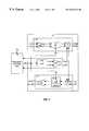
- FIG. 1is a system-level block diagram of a radio transceiver, in accordance with an embodiment of the present invention
- FIG. 2is a circuit diagram of the Voltage-Controlled Oscillator (VCO) shown in FIG. 1;
- VCOVoltage-Controlled Oscillator
- FIG. 3is a circuit diagram of the radio receiver shown in FIG. 1;
- FIG. 4is a circuit diagram of the radio transmitter shown in FIG. 1 .
- FIG. 1is a system-level diagram of a specific example of implementation of a radio signal processing device, in accordance with the present invention.
- this radio signal processing deviceis a radio transceiver, for receiving and transmitting RF signals from and to remote devices.
- the transceiver 100includes primarily a receiver 102 , a transmitter 104 and a shared Voltage-Controlled Oscillator (VCO) 106 .
- Image Reject Filters (IRF) 112 and 118are integrated into the receiver 102 and the transmitter 104 , respectively.
- An external frequency control unit 108is coupled to the VCO 106 , responsible for generating and providing to the VCO 106 a control voltage V freq at output 126 .
- the frequency control unit 108may be implemented as an integral component of the transceiver 100 .
- Differential transmission lines 144 , 146convey the Local Oscillator (LO) signal, output by the VCO 106 , to mixer 114 of the receiver 102 and to mixer 122 of the transmitter 104 .
- Mixer 114is responsible for converting RF signals to lower frequency IF signals, while mixer 122 is responsible for converting IF signals to higher frequency RF signals.
- the radio transceiver 100 chipis fabricated by IBM using a technology known as SiGe HBT. This is only an example of implementation as other possibilities also exist. Note that the architecture of the transceiver 100 is fully differential in order to reduce common-mode (even harmonic) effects, minimize on-chic cross-talk and reduce the impact of ground inductance.
- the receiver 102also includes a Low-Noise Amplifier (LNA) 110 .
- LNALow-Noise Amplifier
- Incoming RF signals arriving at the receiver 102 over differential transmission lines 132 , 134are input to the LNA 110 , which drives the mixer 114 .
- the IRF 112is integrated into the structure of the receiver 102 , as will be described in further detail below.
- the transmitter 104also includes a linear Power Amplifier (PA) 116 .
- PAlinear Power Amplifier
- the IRF 118is integrated into the structure of the transmitter 102 by connection to an amplifier driver 120 , as will be described in further detail below.
- Outgoing RF signalsare output from the PA 116 of the transmitter 104 over differential transmission lines 136 , 138 .
- the frequency control unit 108includes a feedback loop, or Phase-Locked Loop (PLL), that automatically develops a low-frequency control voltage for the VCO 106 , specifically V freq 126 .
- the frequency control unit 108is digitally set by a Digital Frequency Control (DFC) signal 124 .
- DFCDigital Frequency Control
- the DFC signal 124determines the control voltage V freq output by the frequency control unit 108 , which itself sets the LO frequency in the VCO 106 .
- the VCO 106is designed such that the LO frequency is variable over a certain frequency range, where the particular LO frequency at which the VCO 106 operates at any given time is determined by the control voltage V freq 126 . In a specific example, this frequency range is 350 MHz.
- the structure and functionality of such a frequency control unitis well known to those skilled in the art and will not be described in further detail.
- this IRFin order for an IRF to accomplish its task of rejecting the image signal, this IRF must act at a frequency on one side of the LO frequency of the transceiver which directly mirrors the desired signal frequency on the other side of the LO frequency. Consequently, where the desired signal frequency is tunable over a range of frequencies, the IRF must be tunable over a mirror range of frequencies on the other side of the LO frequency.
- IRF 112 and IRF 118both receive the control voltage V freq 126 , specifically at inputs 140 and 142 , respectively. Consequently, as the LO frequency of the VCO 106 is digitally set by the frequency control unit 108 via control voltage V freq 126 , the IRFs 112 and 118 are simultaneously tuned to an image reject frequency by the control voltage V freq 126 . As the LO frequency of the VCO 106 varies with respect to the control voltage V freq 126 , the image reject frequency automatically tracks the LO frequency so as to maintain a fixed frequency separation between the LO frequency and the image reject frequency. Thus, a fixed IF frequency is maintained in the transceiver 100 and automatic tuning of the image reject frequency in the radio transceiver 100 is obtained using a tuning voltage (V freq ) that is already available within the transceiver 100 for other purposes.
- V freqtuning voltage
- the tracking of the VCO 106 LO frequency by the image reject frequency of the IRFs 112 and 118is ensured by the structural design of the IRFs 112 and 118 .
- IRF 112 and IRF 118are designed such that they have a center frequency (image reject frequency) one IF frequency offset from the LO frequency of the VCO 106 , on the opposite side of the LO frequency from the desired RF signal.
- the value of the IF frequencycorresponds to the frequency separation between the image reject frequency and the LO frequency.
- the structural implementation of the IRFs 112 , 118will be described in further detail below.
- the IRFs 112 , 118are designed to track the VCO 106 by using the same resonant tank structure for all three components, including similar inductor designs and capacitor structures.
- each of the VCO 106 , the IRF 112 and the IRF 118includes a resonator, for establishing a frequency within the particular component. This frequency is the LO frequency in the VCO 106 , and the image reject frequency in the IRFs 112 and 118 .
- the same basic circuit topologyis employed for all three resonators, as will be described in further detail below.
- the image rejection frequency in the IRFs 112 , 118automatically tracks the LO frequency, and thus the desired RF frequency.
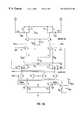
- the VCO 106has a circuit topology as shown in FIG. 2, specifically a differential LC-varactor resonant circuit architecture.
- the term “varactor”refers to a semi-conductor device having a varying reactance.
- V freqis input to the VCO 106 .
- a current mirror formed of BJT transistors 202 , 204 and 206generates the bias current I cs of the BJT pair 208 , 210 .
- the latteralong with inductors 212 , 214 , capacitors 216 , 218 , 228 and varactor diodes 220 , 222 form an LC-tuned Colpitts oscillator, for generating the frequency of oscillation of the VCO 106 (LO frequency).
- the differential LO signal generated by the VCO 106is output at nodes 128 , 130 .
- the oscillatoroscillates because capacitance from emitter to ground of the BJTs 208 , 210 appears as negative resistance to base currents. Note that many different oscillator configurations exist and may be used to implement the VCO 106 .
- IRFs 112 , 118assume that a notch filter approach is used. Alternatively, a bandpass filter approach may be taken. These different types of filters will not be described in further detail, as they are well known to those skilled in the art and have been well documented.
- a similar LC-varactor resonant circuit architecture as in the VCO 106 of FIG. 2is used for the IRFs 112 , 118 .
- the ends of inductors 212 , 214notably nodes 224 and 226 , respectively, are disconnected and instead connected differentially inside stages of the receiver 102 (in the case of the IRF 112 ) and the transmitter 104 (in the case of the IRF 118 ).
- FIG. 3is a circuit diagram representative of an example of implementation of the receiver 102 , including the LNA 110 and the mixer 114 .
- An incoming RF signalis input to the LNA 110 at differential inputs 132 , 134 , and output after amplification at differential outputs 300 , 302 .
- This signalthen drives the mixer 114 at differential inputs 304 , 306 .
- the LO signal from the VCO 106is input to the mixer 114 at differential inputs 144 , 146 .
- Nodes 308 , 310are the connection points at which the IRF 112 is integrated into the receiver 102 , for effecting image signal rejection. Assuming that the circuit architecture shown in FIG.
- the mixer 114is a Gilbert cell mixer quad, where the IRF 112 is connected at the emitters of the four BJTs, also referred to as emitter bridge diodes. The mixer 114 outputs an IF signal at differential outputs 148 , 150 .
- FIGS. 4A and 4Bshow a circuit diagram representative of an example of implementation of the transmitter 104 , including the power amplifier 116 , the amplifier driver 120 and the mixer 122 .
- An IF signalis input to the mixer at differential inputs 152 , 154 .
- the LO signal from the VCO 106is input to the mixer at differential inputs 144 , 146 .
- An RF signalis output from the mixer at differential outputs 404 , 406 and input to the amplifier driver 120 at differential inputs 408 , 410 .
- the IRF 118is connected to the amplifier driver 120 at nodes 400 , 402 , specifically at the emitters of the common-base BJT pair of the amplifier driver 120 . Assuming now that the circuit architecture shown in FIG.
- IRF 118provides a short circuit to ground for image frequency currents, and is used to attenuate the image signal caused by the mixing of the transmit IF signal and the LO signal.
- the amplifier driver 120outputs the signal at differential outputs 412 , 414 , which drives the power amplifier 116 at differential inputs 416 , 418 .
- the power amplifieritself outputs the amplified signal from the transmitter 104 at differential outputs 136 , 138 .
- the tunable IRF 112is integrated into the receiver 102 .
- the IRF 112is incorporated contiguously within the mixer 114 , forming a tunable image reject mixer, where the IRF 112 consists in a tunable LC series resonance placed at the emitters of the mixer 114 bridge network that does the actual mixing.
- Such a filter implementationaffords an important improvement in linearity/noise trade-off with respect to prior art designs in which an additional amplifier stage is needed between the LNA 110 and the mixer 114 to provide an insertion point for the IRF 112 .
- the additional amplifier stageleads to an unfavorable linearity/noise figure trade-off because of the extra gain.
- the resultis that there is sufficient gain up to the point of connection that the LNA 110 may drive the RF signal into the mixer 114 in a conventional fashion, and a favorable balance between gain and noise figure is possible.
- tunable image reject mixermay be used in different circuits to perform image signal rejection, independent from the above-described radio transceiver implementation.
- Such a tunable image reject mixeraffords important advantages over prior art designs, specifically a decrease in power consumption, noise and chip area.
- the performance of the above-described example of implementation of a radio transceiver 100has been simulated and measured in a laboratory.
- the resultsreveal that the present invention allows for monolithic tracking of the image reject filters 112 , 118 on the transceiver 100 , such that more than 40 dB of image rejection, tunable over 350 MHz, is achieved on-chip over a 20 MHz-wide channel.
- Accurate trackingis achieved whereby the notch frequency of IRFs 112 , 118 is kept well centered in order to automatically reject the image signal frequency as the transmitter 104 and receiver 102 RF frequency is changed.
- the radio signal processing device 100may include only one of the receiver 102 and the transmitter 104 . Specifically, the radio signal processing device 100 may be operative to receive but not transmit RF signals (receiver 102 only), or it may be operative to transmit but not receive RF signals (transmitter 104 only). In either situation, tracking of the VCO 106 LO frequency by the image reject frequency of the IRF ( 112 in receiver 102 or 118 in transmitter 104 ) is implemented as described above, such that tunable image signal rejection is achieved in the radio signal processing device.
Landscapes
- Engineering & Computer Science (AREA)
- Computer Networks & Wireless Communication (AREA)
- Signal Processing (AREA)
- Superheterodyne Receivers (AREA)
- Transceivers (AREA)
Abstract
Description
Claims (16)
Priority Applications (1)
| Application Number | Priority Date | Filing Date | Title |
|---|---|---|---|
| US09/366,316US6542724B1 (en) | 1999-08-02 | 1999-08-02 | Method and apparatus for performing image signal rejection |
Applications Claiming Priority (1)
| Application Number | Priority Date | Filing Date | Title |
|---|---|---|---|
| US09/366,316US6542724B1 (en) | 1999-08-02 | 1999-08-02 | Method and apparatus for performing image signal rejection |
Publications (1)
| Publication Number | Publication Date |
|---|---|
| US6542724B1true US6542724B1 (en) | 2003-04-01 |
Family
ID=23442524
Family Applications (1)
| Application Number | Title | Priority Date | Filing Date |
|---|---|---|---|
| US09/366,316Expired - LifetimeUS6542724B1 (en) | 1999-08-02 | 1999-08-02 | Method and apparatus for performing image signal rejection |
Country Status (1)
| Country | Link |
|---|---|
| US (1) | US6542724B1 (en) |
Cited By (22)
| Publication number | Priority date | Publication date | Assignee | Title |
|---|---|---|---|---|
| US20010018334A1 (en)* | 2000-02-28 | 2001-08-30 | Mehmet Ipek | Upconverter mixer circuit |
| US20030199259A1 (en)* | 2002-04-22 | 2003-10-23 | Cognio, Inc. | A Tunable Upconverter Mixer With Image Rejection |
| US6681103B1 (en)* | 2000-08-25 | 2004-01-20 | Sige Semiconductor Inc. | On-chip image reject filter |
| US20040116087A1 (en)* | 2002-12-10 | 2004-06-17 | Irf Semiconductor, Inc. | Radio frequency receiver architecture with on-chip tracking intermediate frequency filtering |
| US20040121753A1 (en)* | 2002-04-22 | 2004-06-24 | Cognio, Inc. | Multiple-Input Multiple-Output Radio Transceiver |
| US20040185781A1 (en)* | 1999-10-21 | 2004-09-23 | Shervin Moloudi | System and method for reducing phase noise |
| US20050227652A1 (en)* | 2004-04-07 | 2005-10-13 | Neoreach, Inc. | Low noise amplifier for wireless communications |
| EP1601110A1 (en)* | 2004-05-10 | 2005-11-30 | STMicroelectronics S.A. | Reception circuit in an integrable heterodyne communication system comprising BAW resonators |
| US20060035619A1 (en)* | 2004-08-13 | 2006-02-16 | Nokia Corporation | Single chip LNA and VCO having similar resonant circuit topology and using same calibration signal to compensate for process variations |
| US20060199559A1 (en)* | 2004-12-09 | 2006-09-07 | Ying-Yao Lin | Multi-band rf receiver |
| US7130604B1 (en)* | 2002-06-06 | 2006-10-31 | National Semiconductor Corporation | Harmonic rejection mixer and method of operation |
| US20070142019A1 (en)* | 2005-12-15 | 2007-06-21 | Sven Mattisson | Mixer Circuit and Method |
| US20080152049A1 (en)* | 2006-12-08 | 2008-06-26 | Texas Instruments Deutschland Gmbh | Digital audio broadcast receiver |
| US20090054008A1 (en)* | 2005-01-31 | 2009-02-26 | Matsushita Electric Industrial Co., Ltd. | Multimode communication apparatus |
| US7881688B1 (en)* | 2006-09-29 | 2011-02-01 | Marvell International Ltd. | Method and apparatus for controlling a local oscillator |
| US20110070830A1 (en)* | 2009-09-24 | 2011-03-24 | Convenientpower Hk Ltd | Antenna network for passive and active signal enhancement |
| US20110187318A1 (en)* | 2010-02-03 | 2011-08-04 | Convenientpower Hk Ltd | Power transfer device and method |
| US20110199045A1 (en)* | 2010-02-15 | 2011-08-18 | Convenientpower Hk Ltd | Power transfer device and method |
| US8718563B2 (en) | 1999-10-21 | 2014-05-06 | Broadcom Corporation | System and method for signal limiting |
| WO2015073070A1 (en)* | 2013-11-12 | 2015-05-21 | Raytheon Company | Methods and apparatus for signal sideband receiver/transceiver for phased array radar antenna |
| US20180083473A1 (en)* | 2016-09-16 | 2018-03-22 | Qualcomm Incorporated | Variable capacitor series tuning configuration |
| CN110034770A (en)* | 2017-12-07 | 2019-07-19 | 英飞凌科技股份有限公司 | System and method for radio-frequency filter |
Citations (8)
| Publication number | Priority date | Publication date | Assignee | Title |
|---|---|---|---|---|
| US4523184A (en)* | 1982-09-30 | 1985-06-11 | Sentrol, Inc. | Supervised wireless security system |
| US5371476A (en)* | 1991-11-15 | 1994-12-06 | Rohm Co., Ltd. | Amplifying circuit |
| US5613234A (en)* | 1994-10-28 | 1997-03-18 | Lucent Technologies Inc. | Receive filter using frequency translation for or in cellular telephony base station |
| US5883539A (en)* | 1995-12-08 | 1999-03-16 | Nec Corporation | Differential circuit and multiplier |
| US5963856A (en)* | 1997-01-03 | 1999-10-05 | Lucent Technologies Inc | Wireless receiver including tunable RF bandpass filter |
| US6285865B1 (en)* | 1998-11-12 | 2001-09-04 | Broadcom Corporation | System and method for on-chip filter tuning |
| US6327463B1 (en)* | 1998-05-29 | 2001-12-04 | Silicon Laboratories, Inc. | Method and apparatus for generating a variable capacitance for synthesizing high-frequency signals for wireless communications |
| US6343207B1 (en)* | 1998-11-03 | 2002-01-29 | Harris Corporation | Field programmable radio frequency communications equipment including a configurable if circuit, and method therefor |
- 1999
- 1999-08-02USUS09/366,316patent/US6542724B1/ennot_activeExpired - Lifetime
Patent Citations (8)
| Publication number | Priority date | Publication date | Assignee | Title |
|---|---|---|---|---|
| US4523184A (en)* | 1982-09-30 | 1985-06-11 | Sentrol, Inc. | Supervised wireless security system |
| US5371476A (en)* | 1991-11-15 | 1994-12-06 | Rohm Co., Ltd. | Amplifying circuit |
| US5613234A (en)* | 1994-10-28 | 1997-03-18 | Lucent Technologies Inc. | Receive filter using frequency translation for or in cellular telephony base station |
| US5883539A (en)* | 1995-12-08 | 1999-03-16 | Nec Corporation | Differential circuit and multiplier |
| US5963856A (en)* | 1997-01-03 | 1999-10-05 | Lucent Technologies Inc | Wireless receiver including tunable RF bandpass filter |
| US6327463B1 (en)* | 1998-05-29 | 2001-12-04 | Silicon Laboratories, Inc. | Method and apparatus for generating a variable capacitance for synthesizing high-frequency signals for wireless communications |
| US6343207B1 (en)* | 1998-11-03 | 2002-01-29 | Harris Corporation | Field programmable radio frequency communications equipment including a configurable if circuit, and method therefor |
| US6285865B1 (en)* | 1998-11-12 | 2001-09-04 | Broadcom Corporation | System and method for on-chip filter tuning |
Cited By (42)
| Publication number | Priority date | Publication date | Assignee | Title |
|---|---|---|---|---|
| US20040185781A1 (en)* | 1999-10-21 | 2004-09-23 | Shervin Moloudi | System and method for reducing phase noise |
| US8718563B2 (en) | 1999-10-21 | 2014-05-06 | Broadcom Corporation | System and method for signal limiting |
| US7933555B2 (en)* | 1999-10-21 | 2011-04-26 | Broadcom Corporation | System and method for reducing phase noise |
| US20010018334A1 (en)* | 2000-02-28 | 2001-08-30 | Mehmet Ipek | Upconverter mixer circuit |
| US6681103B1 (en)* | 2000-08-25 | 2004-01-20 | Sige Semiconductor Inc. | On-chip image reject filter |
| US10326501B2 (en) | 2002-04-22 | 2019-06-18 | Ipr Licensing, Inc. | Multiple-input multiple-output radio transceiver |
| US9374139B2 (en) | 2002-04-22 | 2016-06-21 | Ipr Licensing, Inc. | Multiple-input multiple-output radio transceiver |
| US20100099366A1 (en)* | 2002-04-22 | 2010-04-22 | Ipr Licensing, Inc. | Multiple-input multiple-output radio transceiver |
| US6959178B2 (en)* | 2002-04-22 | 2005-10-25 | Ipr Licensing Inc. | Tunable upconverter mixer with image rejection |
| US7636554B2 (en) | 2002-04-22 | 2009-12-22 | Ipr Licensing, Inc. | Multiple-input multiple-output radio transceiver |
| US20030199259A1 (en)* | 2002-04-22 | 2003-10-23 | Cognio, Inc. | A Tunable Upconverter Mixer With Image Rejection |
| US8463199B2 (en) | 2002-04-22 | 2013-06-11 | Ipr Licensing, Inc. | Multiple-input multiple-output radio transceiver |
| US20040121753A1 (en)* | 2002-04-22 | 2004-06-24 | Cognio, Inc. | Multiple-Input Multiple-Output Radio Transceiver |
| US7130604B1 (en)* | 2002-06-06 | 2006-10-31 | National Semiconductor Corporation | Harmonic rejection mixer and method of operation |
| US20040116087A1 (en)* | 2002-12-10 | 2004-06-17 | Irf Semiconductor, Inc. | Radio frequency receiver architecture with on-chip tracking intermediate frequency filtering |
| WO2004068778A3 (en)* | 2003-01-20 | 2004-11-25 | Cognio Inc | A tunable upconverter mixer with image rejection |
| US7266360B2 (en) | 2004-04-07 | 2007-09-04 | Neoreach, Inc. | Low noise amplifier for wireless communications |
| US20050227652A1 (en)* | 2004-04-07 | 2005-10-13 | Neoreach, Inc. | Low noise amplifier for wireless communications |
| US20050266823A1 (en)* | 2004-05-10 | 2005-12-01 | Stmicroelectronics S.A. | Receiver for an integrated heterodyne communication system including BAW-type resonators |
| US7623837B2 (en) | 2004-05-10 | 2009-11-24 | Stmicroelectronics S.A. | Receiver for an integrated heterodyne communication system including BAW-type resonators |
| EP1601110A1 (en)* | 2004-05-10 | 2005-11-30 | STMicroelectronics S.A. | Reception circuit in an integrable heterodyne communication system comprising BAW resonators |
| US7343146B2 (en)* | 2004-08-13 | 2008-03-11 | Nokia Corporation | Single chip LNA and VCO having similar resonant circuit topology and using same calibration signal to compensate for process variations |
| US20080125074A1 (en)* | 2004-08-13 | 2008-05-29 | Nokia Corporation | Single chip LNA and VCO having similar resonant circuit topology and using same calibration signal to compensate for process variations |
| US20060035619A1 (en)* | 2004-08-13 | 2006-02-16 | Nokia Corporation | Single chip LNA and VCO having similar resonant circuit topology and using same calibration signal to compensate for process variations |
| US8150361B2 (en) | 2004-08-13 | 2012-04-03 | Nokia Corporation | Single chip amplifier and oscillator having similar resonant circuit topology |
| US7548734B2 (en)* | 2004-12-09 | 2009-06-16 | Realtek Semiconductor Corp. | Multi-band RF receiver |
| US20060199559A1 (en)* | 2004-12-09 | 2006-09-07 | Ying-Yao Lin | Multi-band rf receiver |
| US7734311B2 (en)* | 2005-01-31 | 2010-06-08 | Panasonic Corporation | Multimode communication apparatus |
| US20090054008A1 (en)* | 2005-01-31 | 2009-02-26 | Matsushita Electric Industrial Co., Ltd. | Multimode communication apparatus |
| US20070142019A1 (en)* | 2005-12-15 | 2007-06-21 | Sven Mattisson | Mixer Circuit and Method |
| US7890076B2 (en)* | 2005-12-15 | 2011-02-15 | Telefonaktiebolaget Lm Ericsson (Publ) | Mixer circuit and method |
| US7881688B1 (en)* | 2006-09-29 | 2011-02-01 | Marvell International Ltd. | Method and apparatus for controlling a local oscillator |
| US20080152049A1 (en)* | 2006-12-08 | 2008-06-26 | Texas Instruments Deutschland Gmbh | Digital audio broadcast receiver |
| US20110070830A1 (en)* | 2009-09-24 | 2011-03-24 | Convenientpower Hk Ltd | Antenna network for passive and active signal enhancement |
| US8301077B2 (en)* | 2009-09-24 | 2012-10-30 | ConvenientPower, Ltd | Antenna network for passive and active signal enhancement |
| US20110187318A1 (en)* | 2010-02-03 | 2011-08-04 | Convenientpower Hk Ltd | Power transfer device and method |
| US8294418B2 (en) | 2010-02-03 | 2012-10-23 | ConvenientPower, Ltd. | Power transfer device and method |
| US20110199045A1 (en)* | 2010-02-15 | 2011-08-18 | Convenientpower Hk Ltd | Power transfer device and method |
| US9400322B2 (en) | 2013-11-12 | 2016-07-26 | Raytheon Company | Methods and apparatus for signal sideband receiver/transceiver for phased array radar antenna |
| WO2015073070A1 (en)* | 2013-11-12 | 2015-05-21 | Raytheon Company | Methods and apparatus for signal sideband receiver/transceiver for phased array radar antenna |
| US20180083473A1 (en)* | 2016-09-16 | 2018-03-22 | Qualcomm Incorporated | Variable capacitor series tuning configuration |
| CN110034770A (en)* | 2017-12-07 | 2019-07-19 | 英飞凌科技股份有限公司 | System and method for radio-frequency filter |
Similar Documents
| Publication | Publication Date | Title |
|---|---|---|
| US6542724B1 (en) | Method and apparatus for performing image signal rejection | |
| US7518458B2 (en) | Oscillator and data processing equipment using the same and voltage control oscillator and data processing equipment using voltage control oscillator | |
| Stetzler et al. | A 2.7-4.5 V single chip GSM transceiver RF integrated circuit | |
| US6990327B2 (en) | Wideband monolithic tunable high-Q notch filter for image rejection in RF application | |
| US7839229B2 (en) | Voltage-controlled oscillator and communication device using the same | |
| US5187450A (en) | Voltage controlled oscillator suitable for complete implementation within a semiconductor integrated circuit | |
| US6681103B1 (en) | On-chip image reject filter | |
| US20060097801A1 (en) | Oscillator and communication device | |
| US7532055B2 (en) | CMOS-based receiver for communications applications | |
| US6922108B2 (en) | Active balun circuit for single-ended to differential RF signal conversion with enhanced common-mode rejection | |
| US6628170B2 (en) | Low noise amplifier | |
| US20070182502A1 (en) | Push-push voltage controlled oscillator for obtaining differential signals | |
| US8344811B2 (en) | Dual-band voltage-controlled oscillator arrangement | |
| EP0893878B1 (en) | High frequency oscillating circuit | |
| US20100219896A1 (en) | Quadrature Oscillator With High Linearity | |
| US6987425B1 (en) | Low phase noise MOS LC oscillator | |
| US6081167A (en) | Fully integratable voltage controlled oscillator (VCO) circuit | |
| CA2089480C (en) | Oscillator with bias and buffer circuits formed in a die mounted with distributed elements on ceramic substrate | |
| US5418500A (en) | High-frequency oscillator circuit | |
| KR101759780B1 (en) | System and method for a voltage controlled oscillator | |
| Baumberger | A single-chip image rejecting receiver for the 2.44 GHz band using commercial GaAs-MESFET-technology | |
| US5936475A (en) | High-speed ring oscillator | |
| US6754478B1 (en) | CMOS low noise amplifier | |
| US6002303A (en) | Oscillator circuit having a differential configuration and method of forming same | |
| US6690244B2 (en) | Low phase-noise integrated voltage controlled oscillator |
Legal Events
| Date | Code | Title | Description |
|---|---|---|---|
| AS | Assignment | Owner name:NORTEL NETWORKS CORPORATION, CANADA Free format text:ASSIGNMENT OF ASSIGNORS INTEREST;ASSIGNORS:COPELAND, MILES A.;VOINIGESCU, SORIN PETRE;MARCHESAN, DAVID;REEL/FRAME:010326/0222;SIGNING DATES FROM 19990902 TO 19990927 | |
| AS | Assignment | Owner name:NORTEL NETWORKS LIMITED, CANADA Free format text:CHANGE OF NAME;ASSIGNOR:NORTEL NETWORKS CORPORATION;REEL/FRAME:011195/0706 Effective date:20000830 Owner name:NORTEL NETWORKS LIMITED,CANADA Free format text:CHANGE OF NAME;ASSIGNOR:NORTEL NETWORKS CORPORATION;REEL/FRAME:011195/0706 Effective date:20000830 | |
| STCF | Information on status: patent grant | Free format text:PATENTED CASE | |
| FPAY | Fee payment | Year of fee payment:4 | |
| FEPP | Fee payment procedure | Free format text:PAYER NUMBER DE-ASSIGNED (ORIGINAL EVENT CODE: RMPN); ENTITY STATUS OF PATENT OWNER: LARGE ENTITY Free format text:PAYOR NUMBER ASSIGNED (ORIGINAL EVENT CODE: ASPN); ENTITY STATUS OF PATENT OWNER: LARGE ENTITY | |
| FPAY | Fee payment | Year of fee payment:8 | |
| AS | Assignment | Owner name:ROCKSTAR BIDCO, LP, NEW YORK Free format text:ASSIGNMENT OF ASSIGNORS INTEREST;ASSIGNOR:NORTEL NETWORKS LIMITED;REEL/FRAME:027164/0356 Effective date:20110729 | |
| AS | Assignment | Owner name:APPLE INC., CALIFORNIA Free format text:ASSIGNMENT OF ASSIGNORS INTEREST;ASSIGNOR:ROCKSTAR BIDCO, LP;REEL/FRAME:028645/0228 Effective date:20120511 | |
| FPAY | Fee payment | Year of fee payment:12 |