US6542663B1 - Coupling control in side-polished fiber devices - Google Patents
Coupling control in side-polished fiber devicesDownload PDFInfo
- Publication number
- US6542663B1 US6542663B1US09/949,070US94907001AUS6542663B1US 6542663 B1US6542663 B1US 6542663B1US 94907001 AUS94907001 AUS 94907001AUS 6542663 B1US6542663 B1US 6542663B1
- Authority
- US
- United States
- Prior art keywords
- fiber
- cladding
- substrate
- refractive index
- core
- Prior art date
- Legal status (The legal status is an assumption and is not a legal conclusion. Google has not performed a legal analysis and makes no representation as to the accuracy of the status listed.)
- Expired - Lifetime
Links
Images


Classifications
- G—PHYSICS
- G02—OPTICS
- G02B—OPTICAL ELEMENTS, SYSTEMS OR APPARATUS
- G02B6/00—Light guides; Structural details of arrangements comprising light guides and other optical elements, e.g. couplings
- G02B6/24—Coupling light guides
- G02B6/26—Optical coupling means
- G02B6/35—Optical coupling means having switching means
- G02B6/3536—Optical coupling means having switching means involving evanescent coupling variation, e.g. by a moving element such as a membrane which changes the effective refractive index
- G—PHYSICS
- G02—OPTICS
- G02B—OPTICAL ELEMENTS, SYSTEMS OR APPARATUS
- G02B6/00—Light guides; Structural details of arrangements comprising light guides and other optical elements, e.g. couplings
- G02B6/10—Light guides; Structural details of arrangements comprising light guides and other optical elements, e.g. couplings of the optical waveguide type
- G02B6/12—Light guides; Structural details of arrangements comprising light guides and other optical elements, e.g. couplings of the optical waveguide type of the integrated circuit kind
- G02B6/12007—Light guides; Structural details of arrangements comprising light guides and other optical elements, e.g. couplings of the optical waveguide type of the integrated circuit kind forming wavelength selective elements, e.g. multiplexer, demultiplexer
- G—PHYSICS
- G02—OPTICS
- G02B—OPTICAL ELEMENTS, SYSTEMS OR APPARATUS
- G02B6/00—Light guides; Structural details of arrangements comprising light guides and other optical elements, e.g. couplings
- G02B6/24—Coupling light guides
- G02B6/26—Optical coupling means
- G02B6/28—Optical coupling means having data bus means, i.e. plural waveguides interconnected and providing an inherently bidirectional system by mixing and splitting signals
- G02B6/2804—Optical coupling means having data bus means, i.e. plural waveguides interconnected and providing an inherently bidirectional system by mixing and splitting signals forming multipart couplers without wavelength selective elements, e.g. "T" couplers, star couplers
- G02B6/2821—Optical coupling means having data bus means, i.e. plural waveguides interconnected and providing an inherently bidirectional system by mixing and splitting signals forming multipart couplers without wavelength selective elements, e.g. "T" couplers, star couplers using lateral coupling between contiguous fibres to split or combine optical signals
- G02B6/2826—Optical coupling means having data bus means, i.e. plural waveguides interconnected and providing an inherently bidirectional system by mixing and splitting signals forming multipart couplers without wavelength selective elements, e.g. "T" couplers, star couplers using lateral coupling between contiguous fibres to split or combine optical signals using mechanical machining means for shaping of the couplers, e.g. grinding or polishing
- G—PHYSICS
- G02—OPTICS
- G02B—OPTICAL ELEMENTS, SYSTEMS OR APPARATUS
- G02B6/00—Light guides; Structural details of arrangements comprising light guides and other optical elements, e.g. couplings
- G02B6/24—Coupling light guides
- G02B6/26—Optical coupling means
- G02B6/28—Optical coupling means having data bus means, i.e. plural waveguides interconnected and providing an inherently bidirectional system by mixing and splitting signals
- G02B6/293—Optical coupling means having data bus means, i.e. plural waveguides interconnected and providing an inherently bidirectional system by mixing and splitting signals with wavelength selective means
- G02B6/29331—Optical coupling means having data bus means, i.e. plural waveguides interconnected and providing an inherently bidirectional system by mixing and splitting signals with wavelength selective means operating by evanescent wave coupling
- G02B6/29332—Wavelength selective couplers, i.e. based on evanescent coupling between light guides, e.g. fused fibre couplers with transverse coupling between fibres having different propagation constant wavelength dependency
- G02B6/29334—Grating-assisted evanescent light guide couplers, i.e. comprising grating at or functionally associated with the coupling region between the light guides, e.g. with a grating positioned where light fields overlap in the coupler
- G—PHYSICS
- G02—OPTICS
- G02B—OPTICAL ELEMENTS, SYSTEMS OR APPARATUS
- G02B6/00—Light guides; Structural details of arrangements comprising light guides and other optical elements, e.g. couplings
- G02B6/24—Coupling light guides
- G02B6/26—Optical coupling means
- G02B6/28—Optical coupling means having data bus means, i.e. plural waveguides interconnected and providing an inherently bidirectional system by mixing and splitting signals
- G02B6/293—Optical coupling means having data bus means, i.e. plural waveguides interconnected and providing an inherently bidirectional system by mixing and splitting signals with wavelength selective means
- G02B6/29346—Optical coupling means having data bus means, i.e. plural waveguides interconnected and providing an inherently bidirectional system by mixing and splitting signals with wavelength selective means operating by wave or beam interference
- G02B6/2935—Mach-Zehnder configuration, i.e. comprising separate splitting and combining means
- G02B6/29352—Mach-Zehnder configuration, i.e. comprising separate splitting and combining means in a light guide
- G02B6/29355—Cascade arrangement of interferometers
- G—PHYSICS
- G02—OPTICS
- G02B—OPTICAL ELEMENTS, SYSTEMS OR APPARATUS
- G02B6/00—Light guides; Structural details of arrangements comprising light guides and other optical elements, e.g. couplings
- G02B6/24—Coupling light guides
- G02B6/26—Optical coupling means
- G02B6/30—Optical coupling means for use between fibre and thin-film device
- G—PHYSICS
- G02—OPTICS
- G02B—OPTICAL ELEMENTS, SYSTEMS OR APPARATUS
- G02B6/00—Light guides; Structural details of arrangements comprising light guides and other optical elements, e.g. couplings
- G02B6/24—Coupling light guides
- G02B6/26—Optical coupling means
- G02B6/264—Optical coupling means with optical elements between opposed fibre ends which perform a function other than beam splitting
- G02B6/266—Optical coupling means with optical elements between opposed fibre ends which perform a function other than beam splitting the optical element being an attenuator
- G—PHYSICS
- G02—OPTICS
- G02B—OPTICAL ELEMENTS, SYSTEMS OR APPARATUS
- G02B6/00—Light guides; Structural details of arrangements comprising light guides and other optical elements, e.g. couplings
- G02B6/24—Coupling light guides
- G02B6/26—Optical coupling means
- G02B6/28—Optical coupling means having data bus means, i.e. plural waveguides interconnected and providing an inherently bidirectional system by mixing and splitting signals
- G02B6/2804—Optical coupling means having data bus means, i.e. plural waveguides interconnected and providing an inherently bidirectional system by mixing and splitting signals forming multipart couplers without wavelength selective elements, e.g. "T" couplers, star couplers
- G02B6/2852—Optical coupling means having data bus means, i.e. plural waveguides interconnected and providing an inherently bidirectional system by mixing and splitting signals forming multipart couplers without wavelength selective elements, e.g. "T" couplers, star couplers using tapping light guides arranged sidewardly, e.g. in a non-parallel relationship with respect to the bus light guides (light extraction or launching through cladding, with or without surface discontinuities, bent structures)
- G—PHYSICS
- G02—OPTICS
- G02B—OPTICAL ELEMENTS, SYSTEMS OR APPARATUS
- G02B6/00—Light guides; Structural details of arrangements comprising light guides and other optical elements, e.g. couplings
- G02B6/24—Coupling light guides
- G02B6/26—Optical coupling means
- G02B6/35—Optical coupling means having switching means
- G02B6/3502—Optical coupling means having switching means involving direct waveguide displacement, e.g. cantilever type waveguide displacement involving waveguide bending, or displacing an interposed waveguide between stationary waveguides
- G—PHYSICS
- G02—OPTICS
- G02B—OPTICAL ELEMENTS, SYSTEMS OR APPARATUS
- G02B6/00—Light guides; Structural details of arrangements comprising light guides and other optical elements, e.g. couplings
- G02B6/24—Coupling light guides
- G02B6/26—Optical coupling means
- G02B6/35—Optical coupling means having switching means
- G02B6/354—Switching arrangements, i.e. number of input/output ports and interconnection types
- G02B6/356—Switching arrangements, i.e. number of input/output ports and interconnection types in an optical cross-connect device, e.g. routing and switching aspects of interconnecting different paths propagating different wavelengths to (re)configure the various input and output links
- G—PHYSICS
- G02—OPTICS
- G02B—OPTICAL ELEMENTS, SYSTEMS OR APPARATUS
- G02B6/00—Light guides; Structural details of arrangements comprising light guides and other optical elements, e.g. couplings
- G02B6/24—Coupling light guides
- G02B6/26—Optical coupling means
- G02B6/35—Optical coupling means having switching means
- G02B6/3564—Mechanical details of the actuation mechanism associated with the moving element or mounting mechanism details
- G02B6/3582—Housing means or package or arranging details of the switching elements, e.g. for thermal isolation
- G—PHYSICS
- G02—OPTICS
- G02B—OPTICAL ELEMENTS, SYSTEMS OR APPARATUS
- G02B6/00—Light guides; Structural details of arrangements comprising light guides and other optical elements, e.g. couplings
- G02B6/24—Coupling light guides
- G02B6/26—Optical coupling means
- G02B6/35—Optical coupling means having switching means
- G02B6/3564—Mechanical details of the actuation mechanism associated with the moving element or mounting mechanism details
- G02B6/3584—Mechanical details of the actuation mechanism associated with the moving element or mounting mechanism details constructional details of an associated actuator having a MEMS construction, i.e. constructed using semiconductor technology such as etching
- G—PHYSICS
- G02—OPTICS
- G02B—OPTICAL ELEMENTS, SYSTEMS OR APPARATUS
- G02B6/00—Light guides; Structural details of arrangements comprising light guides and other optical elements, e.g. couplings
- G02B6/24—Coupling light guides
- G02B6/36—Mechanical coupling means
- G02B6/3628—Mechanical coupling means for mounting fibres to supporting carriers
- G02B6/3632—Mechanical coupling means for mounting fibres to supporting carriers characterised by the cross-sectional shape of the mechanical coupling means
- G02B6/3636—Mechanical coupling means for mounting fibres to supporting carriers characterised by the cross-sectional shape of the mechanical coupling means the mechanical coupling means being grooves
- G—PHYSICS
- G02—OPTICS
- G02B—OPTICAL ELEMENTS, SYSTEMS OR APPARATUS
- G02B6/00—Light guides; Structural details of arrangements comprising light guides and other optical elements, e.g. couplings
- G02B6/24—Coupling light guides
- G02B6/36—Mechanical coupling means
- G02B6/3628—Mechanical coupling means for mounting fibres to supporting carriers
- G02B6/3684—Mechanical coupling means for mounting fibres to supporting carriers characterised by the manufacturing process of surface profiling of the supporting carrier
- G02B6/3692—Mechanical coupling means for mounting fibres to supporting carriers characterised by the manufacturing process of surface profiling of the supporting carrier with surface micromachining involving etching, e.g. wet or dry etching steps
Definitions
- This applicationrelates to optical fiber devices, and more specifically, to devices based on evanescent optical coupling between two fibers.
- Optical wavesmay be transported through optical waveguiding elements or “light pipes” such as optical fibers.
- a typical fibermay be simplified as a fiber core and a cladding layer surrounding the fiber core.
- the refractive index of the fiber coreis higher than that of the fiber cladding to confine the light.
- Light rays that are coupled into the fiber core within a maximum angle with respect to the axis of the fiber coreare totally reflected at the interface of the fiber core and the cladding. This total internal reflection provides a mechanism for spatially confining the optical energy of the light rays in one or more selected fiber modes to guide the optical energy along the fiber core.
- Optical fibersmay be used in transmission and delivery of optical signals from one location to another in a variety of optical systems, including but not limited to, fiber devices, fiber links and fiber networks for data communications and telecommunications.
- optical fibersmay be used to form various optical devices to modify, filter, or process guided optical energy.
- the guided optical energy in a fiberis not completely confined within the core of the fiber.
- a portion of the optical energycan “leak” through the interface between the fiber core and the cladding via an evanescent field that essentially decays exponentially with the distance from the core-cladding interface.
- the distance for a decay in the electric field of the guided light by a factor of e ⁇ 2.718is about one wavelength of the guided optical energy.
- This evanescent leakagemay be used to couple optical energy into or out of the fiber core, or alternatively, to perturb the guided optical energy in the fiber core.
- a fiber deviceincludes a substrate having first and second opposing substrate surfaces and including an elongated groove formed over the first substrate surface, and a fiber having a fiber coupling portion engaged in the elongated groove. A portion of fiber cladding of the fiber coupling portion is removed to form a side fiber surface spaced from a fiber core of the fiber within a reach of an evanescent field of a guided mode in the fiber.
- the fiber coupling portionhas a fiber cladding portion whose radial index distribution is different from adjacent fiber portions to produce a radial mode profile wider than a radial mode profile of the adjacent fiber portions.
- a methodincludes selecting a fiber portion of a fiber, removing a portion of fiber cladding of the selected fiber portion to form a fiber coupling surface spaced from a fiber core of the selected fiber portion within a reach of an evanescent field of a guided mode, and modifying a property of said selected fiber portion.
- the modificationincreases a cladding refractive index of the selected fiber portion and to increase a spatial mode profile of said guided mode in the selected fiber portion to be greater than a spatial mode profile of the guided mode in an adjacent fiber portion whose cladding refractive index is not modified.
- FIG. 1shows one embodiment of a fiber device that integrates or engages a fiber to a substrate with a groove for positioning the fiber and openings for holding the fiber.
- FIGS. 2A and 2Bshow a cross sectional view of the device in FIG. 1 along the direction AA′ and a side view of the device in FIG. 1 along the direction BB′, respectively.
- FIGS. 3A and 3Bshow examples of two different cross sections for grooves shown in FIG. 1 .
- FIGS. 4A, 4 B, 5 A, 5 B, 5 C, 5 D, and 5 Eillustrate a process of fabricating V grooves in semiconductor substrates by anistropic etching.
- FIG. 6illustrates formation of openings in V grooves by anistropc etching.
- FIG. 7Ashows a substrate that is fabricated with an array of grooves with openings.
- FIG. 7Bshows a fiber device formed on a substrate with two or more grooves aligned with each other along a straight line on a single side of the substrate.
- FIGS. 7C and 7Dshow fiber devices formed on a substrate with grooves on a single side of substrate that are oriented in different relative directions.
- FIGS. 8A, 8 B, 8 C, 8 D, and 9illustrate substrates that are processed with grooves on both substrate surfaces.
- FIG. 10shows a substrate processed with grooves on both substrate surfaces, where openings at both ends of each groove are separately fabricated from the V grooves.
- FIGS. 11 and 12show exemplary fiber devices by integrating fibers to substrates with grooves.
- FIG. 13Ashows uses of relative positions between grooves to control optical coupling between fibers positioned in the grooves.
- FIG. 13Bshows a substrate with both deep and shallow grooves formed on a single side.
- FIG. 13Cshows a substrate with both deep and shallow grooves formed on both sides.
- FIG. 14shows an exemplary fiber device that has lateral jump-channel grooves on the substrate to change a direction of a fiber in the substrate plane.
- FIG. 15shows a design to engage a side-polished fiber onto a substrate by using an elongated groove with a single through hole.
- FIG. 16shows one embodiment of a fiber coupler based on evanescent coupling between two side-polished fibers engaged to two different substrates.
- FIG. 17illustrates a cross sectional view of the fiber coupling region along lines AA of the device in FIG. 16 .
- FIG. 18illustrates spatial expansion of a guided mode in a fiber due to increasing the cladding index of the fiber.
- FIG. 19shows the index modification process according to one embodiment.
- FIG. 20shows a gradual profile along a longitudinal direction of the fiber of the cladding index as a result of the index modification.
- FIG. 21shows that the radial mode profile of a fiber, after the index modification, varies along the fiber from one side of the side-polished fiber coupling port to the other side.
- FIG. 22shows a use of radiation exposure to modify the cladding index in a fiber that has a radiation-sensitive cladding material.
- FIG. 23shows an ion,exchange process to modify the cladding index in a fiber.
- FIG. 24shows a grating formed in the fiber coupling port of a side-polished fiber engaged to a substrate.
- the devices and techniques of this applicationuse at least one fiber integrated on or engaged to a substrate fabricated with one or more grooves. One portion of the cladding of this fiber is removed and polished to form a fiber coupling port.
- the fiber coupling porthas a surface that is sufficiently close to the fiber core so that optical energy can be coupled through via evanescent fields out of or into the fiber core.
- techniques for modifying the refractive index of the fiber claddingare disclosed to improve the fabrication tolerance in the spacing between two coupled fibers.
- FIG. 1shows one embodiment of a fiber device 100 where a fiber 140 is integrated or engaged to a substrate 110 .
- the fiber device 100may be used as a building block to construct a variety of fiber devices, including but not limited to, fiber couplers, fiber attenuators, fiber modulators, fiber beam splitters, optical fiber switches, and fiber frequency-division multiplexers.
- FIGS. 2A and 2Bshow additional details of the fiber device 100 .
- the substrate 110may be formed of various materials, such as semiconductors, insulators including dielectric materials (e.g., a glass, a quartz, a crystal, etc), metallic materials, or any other solid-state materials that can be processed to form the device features such as grooves and through holes disclosed herein.
- Two parallel and opposing substrate surfaces, 112 and 114are generally flat and may be polished.
- An elongated groove 120is formed in the substrate 110 on the surface 112 and is essentially a recess from the surface 112 .
- the groove 120may be fabricated by removing a portion of the material from the substrate 110 through etching or other processes.
- the geometry of the groove 120is generally elongated along a straight line as illustrated or along a curved line. Unless otherwise indicated, the following description will use straight-line grooves as examples. Some embodiments are described with specific reference to groove with V-shaped cross sections as shown by the groove 310 in FIG. 3 B.
- the cross sectionsare generally not so limited and may also be other shapes as well, including rectangular as shown in FIG. 2A, U-shaped as shown by the groove 310 in FIG. 3A, a circularly shape or other suitable shapes.
- the width, W, of the groove 120is generally greater than the diameter, d, of the fiber 140 and may either remain a constant or vary spatially along the groove 120 , e.g., increasing from the center towards the two ends.
- the length, L, of the groove 120may vary from one grove to another and can be determined based on specific requirements of applications.
- the depth D of the groove 120may be a constant or may vary along the groove 120 , e.g., increasing from the center towards the two ends. In general, at least a portion of the groove 120 has a depth D to expose a portion of the fiber cladding of the fiber 140 above the surface 112 while still keeping the fiber core below the surface 112 . Sometimes, the depth D of the groove 120 may also be selected to expose the fiber core.
- the groove 120may have a different depth so that the fiber can be placed within the groove 120 under the substrate surface 112 .
- the depth D of the entire groove 120may be greater than fiber diameter d.
- portions of the groove 120may have a depth that is at least the fiber diameter d so that the fiber can be essentially placed in the groove 120 below the surface 112 .
- the depth D of the entire groove 120may be greater than fiber diameter d.
- the following descriptionwill assume that at least a portion of a groove 120 to expose a portion of the fiber cladding above the surface 112 and adjacent portions sufficiently deep to keep the fiber below the surface 112 .
- the central portion of the groove 120may have a depth D less than d but greater than (d+dc)/2 while the portions on either sides of the central portion may have a depth equal to or greater than the fiber diameter d.
- the fiber device 100includes two openings 131 and 132 that are respectively formed at the two ends of the groove 120 and penetrate through the substrate 110 .
- the openings 131 and 132are through holes extending between the two surfaces 112 and provide access from one surface ( 112 or 114 ) to another.
- the spacing between the openings 131 and 132essentially determines the length L of the groove 120 .
- the aperture of the openings 131 and 132should be sufficiently large to receive the fiber 140 , e.g., with a diameter greater than the diameter of the fiber 140 .
- the shape of the holes 131 and 132may generally be in any suitable geometry.
- a portion of the fiber 140is placed in the groove 120 near the surface 112 .
- the remaining portions 141 , 142 of the fiber 140 on both sides of the portion in the groove 120are respectively fed through the first and second openings 131 , 132 to the other side 114 of the substrate 110 .
- the fiber 140may be slightly pulled by moving the fiber portions 141 and 142 in opposite directions so that the portion of the fiber 140 in the groove 120 is in substantially full contact with the groove 120 .
- the cladding of the fiber 140 in this portionprotrudes out of the surface 112 .
- the fiber core in this portion of the fiberis generally kept under the surface 112 .
- the cladding of a central portion of the fiber 140 between the holes 131 and 132may be exposed. This protruded or exposed cladding is then removed and polished to form a flat surface 144 of a length Lc that is above the fiber core 143 and is substantially coplanar with the surface 112 of the substrate 110 .
- the flat surface 144When the spacing, h, between the flat surface 144 and the fiber core 142 is sufficiently small (e.g., on the order of or less than one wavelength of optical energy), the flat surface 144 can be used to couple optical energy into or out of the fiber core 144 through the evanescent fields outside the fiber core.
- the length, Lc, of the flat surface 144approximately represents the optical coupling length for the fiber device 100 .
- This coupling surface 144may also be non-flat, e.g., curved to a certain extent, as long as it can transmit evanescent signals.
- FIGS. 4A and 4Billustrate the fabrication of the V groove 320 and placement of the fiber 140 in the V groove 320 as shown in FIG. 3 B.
- a mask layer 410is deposited over the surface 112 of the substrate 110 and is patterned by a suitable technique such as a photolithography process to have one or more groove areas exposing the underlying substrate 110 .
- the exposed portions of the substrate 110are anistropically etched to form V grooves.
- the substrate 110is formed of a semiconductor, e.g., silicon
- a thermally-grown silicon oxide or nitride filmmay be used as the etching mask 410 for anisotropic silicon etching.
- an etchant chemicalsuch as alkaline (KOH) can be applied on the silicon ( 100 ) surface to produce truncated v-shaped grooves. Since the anisotropic etching is stopped at the crystalline plane ( 111 ), the dimension of the V grooves, such as the groove width and depth can be accurately controlled by properly selecting the dimension of the groove patterns formed in the etching mask 410 .
- the fibers 140can be placed in the grooves 320 and bonded to the groves 320 at locations 420 .
- the bondingmay be implemented by a number of techniques, including but not limited to using an epoxy, glass frit thermal bond, or CO 2 assisted thermal bond.
- an array of fibers 140can be precisely aligned in the grooves 320 with a predetermined spacing.
- the exposed cladding of the fiber 140can then be removed and polished to form the flat surface 144 as shown in FIG. 3 B.
- FIG. 5Ashows one exemplary groove pattern 500 formed in the etching mask layer 430 in FIG. 4 A.
- FIG. 5Billustrates the corresponding V groove 320 in the silicon substrate 110 formed from the anistropic etching by using the mask 500 .
- the opening of the groove pattern 500is designed to gradually widen from the center to both sides along the groove to be formed. Accordingly, the width and depth of the underlying V groove 320 also increase from the center portion 510 to side portions 520 that are spaced from the center along the groove 320 .
- the surfaces of the V groove 320are not flat but are curved as a result of etching through the above mask 500 .
- FIGS. 5C, 5 D, and 5 Eshow the placement of fibers 140 in the above V-groove structure.
- the above anistropic etchingmay be used to form both the V groove 320 and the openings 131 and 132 at both sides of the V groove 320 as shown in FIG. 1 .
- side portions 620 of the V groove 610can extend all the way through the substrate 110 from the surface 112 to the opposite surface 114 and hence create an opening 620 on the surface 114 .
- the openings 620therefore, can be used as the openings 131 and 132 to allow the fiber 140 to go through the substrate 110 from the surface 112 to the opposite surface 114 .
- FIGS. 7A and 7Bshow that an array 700 of such V grooves 710 with two openings can be formed on one side of the substrate 110 .
- the V grooves 710may be aligned to be parallel to one another along their elongated directions and are arranged to form multiple parallel columns 730 with a spacing 740 . Within each column 730 , multiple V grooves 710 may be spaced from one another by a spacing 720 .
- the substrate 110 with the array 700may diced into multiple units each having one or more V grooves 710 . Such units can be used to form various fiber devices. Hence, a batch fabrication process may be used to process the substrate 110 and to simultaneously form multiple fiber devices with V grooves 710 .
- a single fibercan be threaded through different V grooves 710 in a column 730 between the surfaces 112 and 114 via the openings 131 and 132 .
- FIG. 7Bshows an example where the fiber 140 is threaded through V grooves 710 A, 710 B, 710 C, and 710 D formed along a straight line on the surface 112 of the substrate 110 .
- a spacer 721such as a rod, may be optionally positioned on the surface 114 between the openings of two adjacent V grooves to provide a support to the fiber 140 . Such support may be used to reduce sharp bending of the fiber 140 which may damage the fiber 140 .
- a coupling portis formed at each V groove on the surface 112 and is operable to couple optical energy out of or into the fiber 140 . Therefore, this device has multiple coupling ports on the surface 112 to couple optical energy into or out of the fiber 140 .
- optical switching, optical multiplexing, and other coupling operationsmay be achieved.
- FIGS. 7C and 7Dshow additional embodiments of fiber devices that two different grooves 750 and 760 on the substrate 110 are not aligned along a straight line as in FIGS. 7A and 7B but form an angle with respect to each other.
- Numerals 751 , 752 , 761 , and 762indicate the openings of the grooves 750 and 760 that penetrate through the substrate 110 .
- the two grooves 750 and 760are spaced from each other.
- a fibermay be placed in the grooves 750 and 760 by sequentially passing the fiber through the openings 761 , 762 , 752 , and 751 .
- two grooves 750 and 760are share a common opening 752 . Such arrangements may be combined with aligned grooves.
- the groove 120 with its two openings 131 and 132may be formed on both sides 112 and 114 of the substrate 110 in the following manner. First, two adjacent grooves respectively formed in different sides of the substrate are aligned along the same groove direction. Second, the groove on one side shares an opening with the adjacent groove on the opposite side of the substrate 110 . Techniques such as the double-sided photolithography may be used to form the V grooves on both surfaces of the substrate. Unlike the fiber device shown in FIG. 7B where the.coupling ports are only on a single side of the substrate, a substrate with V grooves on both sides can form a fiber device with coupling ports on both sides of the substrate. Such double-sided coupling capability can provide flexible and versatile coupling configurations in various fiber devices.
- FIGS. 8A, 8 B, and 8 Cillustrate one example of a fiber device 800 that has V grooves on both sides 112 and 114 of the substrate 110 .
- a first V groove 820is formed on the side 114 . Similar to the V grooves in FIGS. 5B and 6, the depth and width of the V groove 820 increase from its center towards both ends 820 A and 820 B.
- a second, similar V groove 810is formed on the opposite side 112 along the same groove direction. The end 810 A of the second groove 810 overlaps with the end 820 A of the first V groove 820 to create a through hole 812 that connects the V grooves 810 and 820 .
- a third V groove 830is also shown on the side 112 to have one end 830 A overlap with the end 820 B of the V groove 820 on the opposite side 114 .
- a through hole 822is then formed at the overlapping region to connect the V groove 820 to the V groove 830 .
- a fiber 140is shown in FIG. 8C to thread through the holes 812 and 822 to form coupling ports on both sides 112 and 114 of the substrate 110 .
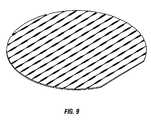
- FIG. 8Dshows a 3-port fiber device 840 that is formed by dicing a linear array of V grooves 810 , 820 , and 830 from the substrate 110 . Comparing to the single-side device shown in FIG. 7B, the natural curvature of the V grooves formed on both sides eliminates the spacers 740 . Similar to the batch fabrication of the single-sided devices shown in FIG. 7A, multiple double-sided devices may also be simultaneously fabricated from a single-sided substrate as illustrated in FIG. 9 .
- two adjacent V grooves, located on opposite sides of the substratemay not be aligned along a straight line but form an angle with each other as illustrated by the adjacent grooves formed on the same side shown in FIGS. 7C and 7D. Similar to the grooves in FIGS. 7A and 7B, two adjacent V grooves, located on opposite sides of the substrate, may also be designed to spatially separate from each other without sharing a common opening that penetrates through the substrate and extends between two sides of the substrate.
- V groovesare formed by anistropically etching for forming the V grooves. Hence, there is no need to use a separate process to fabricate the openings if the etching mask is properly designed. However, a separate fabrication step may also be used to form an opening and to achieve any desired geometric shape of the opening that may be difficult or impossible to make through etching the V grooves.
- FIG. 10illustrates a fiber device 1000 with aligned V grooves 810 , 820 , and 830 on both sides 112 and 114 of the substrate 110 that are spaced from one another by rectangular openings 1010 and 1020 .
- the V grooves 810 and 830are formed on the side 114 and the groove 820 is formed on the opposite surface 112 but is located between the grooves 810 and 830 .
- An etching process separate from etching of the V groovesis needed to form such openings 1010 and 1020 .
- Other processing techniquessuch as laser machining may also be used to form the openings.
- the above fiber devices with V grooves either on one side or two sidesmay be used to form various fiber devices. Some exemplary devices are described below.
- FIG. 11shows an optical fiber coupler 1100 by using two substrates 1110 and 1120 each with V grooves on a single surface of the substrate.
- the substrate 1110has a surface 1110 A on which three V grooves are fabricated and a fiber 140 A is placed therein to form three coupling ports 1111 , 1112 , and 1113 .
- the substrate 1120has a surface 1120 A on which three V grooves are fabricated and a fiber 140 B is placed therein to form three coupling ports 1121 , 1122 , and 1123 .
- the two substrates 1110 and 1120are engaged by having the surfaces 1110 A and 1120 A to face each other.
- the ports on one substratesubstantially overlap with the coupling ports of another substrate to allow energy exchange between the fibers 140 A and 140 B.
- Various techniquesmay be used to engage the two substrates together, such as optical epoxy, glass frit thermal bond, CO2 laser assisted thermal bond.
- a fiber device with V grooves on both sides of the substratecan be used to provide coupling on both sides. More coupling flexibility can be achieved in such a device than a device with grooves on only one side. For example, each fiber in the device 1100 shown in FIG. 11 cannot be accessed from the exposed surfaces 1110 B and 1120 B. Such access would be possible if one of the two substrates 1110 and 1120 were designed to have grooves on both sides. Thus, three or more substrates may be vertically stacked together to form a multi-layer optical coupler. Since each substrate may have two or more fibers, coupling among many fibers in different substrates may be achieved.
- FIG. 12shows a 4-layer optical multi-port coupler 1200 having 4 different double-sided substrates 1201 , 1202 , 1203 , and 1204 based on the designs shown in FIGS. 8D or 10 .
- Four different fibers 1210 , 1220 , 1230 , and 1240are respectively threaded in the substrates 1201 , 1202 , 1203 , and 1204 .
- Two adjacent substrates, such as 1201 and 1202may be coupled to form the coupling ports 1212 , 1214 , and 1216 .
- optical energycan be coupled between any two fibers.
- an optical signal in the fiber 1210may be coupled to the fiber 1230 by first coupling into the fiber 1220 and then coupling from the fiber 1220 into the fiber 1230 .
- a double-sided substratecan interface at both sides with other single-sided or double-sided substrates.
- FIG. 13Aillustrates that optical coupling between two fibers in different layers may be controlled in a number of ways by controlling the relative position of the two fibers in grooves.
- no optical couplingoccurs between fibers 1301 and 1302 in the layers 1201 and 1202 when they are placed in deep grooves to have a separation much greater than one wavelength of the light.
- the fibers 1303 and 1304 in the layers 1202 and 1203are positioned in shallow grooves so that a portion of each fiber's cladding is removed to allow for optical coupling.
- the depth of the grooves for the fibers 1303 and 1304can be controlled to control the coupling strength via evanescent fields.
- the fibers 1305 and 1306also in shallow grooves, are spatially offset in the lateral direction so that the optical coupling is reduced with,the amount of the offset.
- the grooves for holding fibers 1301 and 1302are “deep” grooves in that the depth of the groove is greater than the diameter of the fiber so that the fiber cladding in the fiber portion in such grooves is not exposed above the substrate surface and no optical coupling port is formed.
- the grooves for holding the fibers 1303 , 1304 , 1305 , and 1306are “shallow” grooves as the groove 120 described with reference to FIG. 1 where a portion of a part of the fiber cladding protrudes above the substrate surface when the fiber is placed in such a groove and can be removed to form an optical coupling port 144 .
- Such deep and shallow groovesmay be combined to provide flexibility and versatility in routing fibers and arranging optical coupling ports in a fiber device.
- FIG. 13Bshows a single-sided substrate similar to the substrate in FIG. 7B but processed to have both deep grooves 1312 and shallow grooves 1310 . Each deep grove 1312 is used at a location where optical coupling is undesirable.
- FIG. 13Cshows a double-sided substrate with deep grooves 1330 and shallow grooves 1320 .
- FIG. 14further shows that a lateral jump-channel groove 1424 on a substrate 1400 may be used to change the lateral direction of a fiber.
- the substrate 1400is shown to have grooves on both sides.
- Solid elongated boxes such as 1410represent grooves formed on one side and the dashed elongated boxes such as 1412 represent grooves formed on the other side.
- the grooves 1410 , 1412 , 1414 , 1416 , and 1418are aligned with one another along a straight line to hold a fiber 1401 .
- the groove 1424is a lateral jump-channel groove that is oriented with an angle relative to adjacent grooves 1422 and 1436 .
- a fiber 1402can be threaded through the lateral jump-channel groove 1424 to run through grooves 1440 and 1422 and then to change its direction to run through grooves 1436 and 1438 .
- Lateral jump-channel grooves 1432 and 1444are also shown to direct the fiber 1402 from the groove 1430 to grooves 1456 and 1458 .
- a single-side substrate with grooves on one sidemay also be designed to have such lateral jump-channel grooves.
- Such a lateral jump-channelcan be combined with the vertical integration of different double-side substrates to change the direction of an optical signal both laterally within a substrate and vertically from one substrate to another substrate. This opens up possibility similar to multi-layer printed circuit board technology allowing sophisticated connections from point to point and from layer to layer.
- FIG. 1shows the use of elongated groove 120 and two through holes 131 and 132 at the ends of the groove 120 to engage a fiber to the substrate 110 and to form each fiber coupling port 144 .
- only one through hole 132 in the substrate 110may be used to engage the fiber 140 to form a fiber coupling port 144 .
- FIG. 15shows an example of such a fiber structure 1500 .
- the groove 120may extend to one end side 1510 of the substrate 110 so that one end 141 of the fiber 140 leaves the groove 120 without going through a through hole.
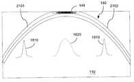
- FIG. 16shows a fiber coupler 1600 that couples two side-polished fibers 140 A and 140 B respectively engaged to two substrates 110 A and 110 B. Both fibers 140 A and 140 B are polished to remove a portion of the fiber cladding and to form the fiber coupling ports 144 A on the substrate surface 112 A and 144 B on the substrate surface 112 B, respectively.
- FIG. 17shows the crosssectional view of the engaged coupling ports 144 A and 144 B along the line AA shown in FIG. 16 .
- the spacing D between the fiber cores 143 A and 143 B of the fibers 140 A and 140 Bshould be set to place one fiber core in the evanescent field of a guided optical wave in another fiber core.
- this spacing Dmay be on the order of one wavelength of the optical signal. For typical wavelengths at about 1.5 micron, the spacing D is generally less than a few microns.
- the fiber coupling ports 144 A and 144 Bmay be formed by using a polishing process.
- One aspect of the present inventionis to modify the refractive index of the fiber cladding in a selected fiber portion of at least one of the fibers 140 A and 140 B to expand the radial spatial extend of the guided mode.
- the radial directionis substantially perpendicular to the longitudinal direction of the fiber.
- FIG. 18illustrates a radial mode profile 1810 of a mode prior to the modification that is similar to the mode in a conventional fiber and a radial profile 1820 of the expanded radial mode profile 1820 after the cladding index has been increased.
- the refractive index of the fiber cladding near the fiber coreis increased to be closer to the index of the fiber core. This effectuates an increase in the mode size.
- the spacing Dcan be increased while still maintaining the evanescent coupling configuration between the fibers 140 A and 140 B.
- This increased spacing Dallows the D to vary in a larger tolerance range in comparison with the tolerance range for D prior to the modification of the cladding indices of the two fibers 140 A and 140 B.
- FIG. 19shows the fabrication process of the fibers 140 A and 140 B.
- a single-mode fiberis provided to have a numerical aperture that is substantially uniform along the fiber and is approximately equal to that of commercial single-mode fibers.
- the radial mode profile of the fiberis small as shown by the mode 1810 in FIG. 18 .
- the fiber cladding of a selected fiber portionis treated to increase the cladding index and hence to achieve the spatially expanded mode as shown by the mode 1820 in FIG. 18 in the treated fiber portion.
- the cladding index in the selected fiber portionis modified to have a gradual profile that changes gradually along the longitudinal direction of the fiber so that this no abrupt change in the cladding index along the fiber to cause adverse optical reflection along the fiber.
- FIG. 19shows the fabrication process of the fibers 140 A and 140 B.
- the cladding indexis high at center of.the fiber coupling port 144 (but still less than the core refractive index) and gradually decreases towards both ends of the fiber coupling port 144 . This trend continues along the fiber until the cladding index of at the edge of the modified region eventually becomes equal to the cladding index of adjacent, unmodified fiber portions.
- the modified fiberhas a varying radial mode profile from one side of the side-polished fiber coupling port to the opposite side because only the fiber cladding in the selected fiber portion, which is in and adjacent to the coupling port 144 , is modified and other fiber portions are not so modified.
- FIG. 21shows that the fiber 140 has a narrow radial mode profile 1810 as in a conventional fiber in the fiber portion 2101 , an expanded radial mode profile 1820 in the fiber coupling port 144 , and the narrow radial mode profile 1810 in the fiber portion 2102 .
- the cladding-modified region with expanded radial mode profile 1820may be limited in one or a few selected regions in the fiber to reduce the overall optical loss.
- the expanded radial mode profile 1820can benefit efficiency of the evanescent coupling and the control of the coupling efficiency but at the same time it can also introduce undesired optical loss due to the expanded mode size in fiber portions where the evanescent coupling is not needed.
- Other fiber portionswhich constitute the majority of the fiber, may preferably have the narrow radial mode profile that approximately matches that of conventional single-mode fibers to allow for efficient interconnection with other fibers by using the end-to-end pigtail fiber connections.
- the fiber device 1600 that couples two fibers 140 A and 140 B as in FIG. 16it may be sufficient to have only one of the fibers 140 A and 140 B to be modified to have a narrower radial mode profile in the coupling port as shown in FIG. 21 while the other fiber is a conventional fiber with a substantially uniform radial mode profile.
- both fibers 140 A and 140 Bmay be made to have the spatial mode distribution as in FIG. 21 .
- One way to modify the cladding indexis to use a radiation-sensitive material to form the fiber cladding in at least the selected fiber portion which is to be processed to form the side-polished fiber coupling port.
- the fiber claddingmay be UV-sensitive and responsive to the UV light to increase its index.
- FIG. 22shows that a fiber 140 may be first engaged to the substrate 110 and polished to form the fiber coupling port 144 . Then, the UV light 2200 is directed to illuminate the fiber portion that includes the fiber coupling port 144 to increase the cladding index.
- the intensity of the UV light 2200may be controlled to have a spatially varying profile along the fiber 140 : the UV light intensity is at a maximum value in the center of the fiber coupling port 144 and gradually decays along the fiber towards both ends of the port 144 .
- the fiber coupling region 144may be first exposed to the UV light 2200 prior to being engaged to the substrate 110 and polished to form the port 144 .
- FIG. 23shows an alternative technique where an ion exchange process may be performed to increase the index of the fiber cladding.
- the fiber 140is engaged to the substrate 110 and is then polished to form the port 144 .
- the ion exchangeis then performed to implant ions in the cladding of the port 144 to increase its index.
- the density of the implanted ionscan be controlled to achieve the desired gradual longitudinal profile as shown in FIG. 20 in the cladding index to reduce undesired optical reflection.
- FIG. 24further shows that, a grating 2400 may be fabricated in the fiber coupling port 144 whose fiber cladding has been modified to achieve the expanded radial mode profile.
- This grating 2400may be formed in the fiber core or in the fiber cladding.
- the grating 2400may be used to select a particular wavelength for evanescent coupling.
- the grating 2400may be a tunable grating to adjust the coupling at the port 144 .
- At least one buffer layer of a suitable material such as a dielectric material like silicon dioxide or silicon nitridemay be formed over a groove under the fiber.
- This buffer layermay be designed to have certain mechanical or thermal properties to stabilize the structure formed by the substrate, the buffer layer, and the fiber by reducing the mechanical or thermal stress between the silicon substrate and the glass fiber. Therefore the reliability of the device can be improved.
- the substrateis formed of silicon
- a dielectric material with a coefficient of thermal expansion (CTE) between the CTE values of the silicon and the glass fibermay be used as the buffer.
- CTEcoefficient of thermal expansion
- Two or more buffer layersmay also be used to achieve desired stabilizing effects.
Landscapes
- Physics & Mathematics (AREA)
- General Physics & Mathematics (AREA)
- Optics & Photonics (AREA)
- Engineering & Computer Science (AREA)
- Microelectronics & Electronic Packaging (AREA)
- Mechanical Coupling Of Light Guides (AREA)
- Optical Couplings Of Light Guides (AREA)
Abstract
Description
Claims (20)
Priority Applications (1)
| Application Number | Priority Date | Filing Date | Title |
|---|---|---|---|
| US09/949,070US6542663B1 (en) | 2000-09-07 | 2001-09-07 | Coupling control in side-polished fiber devices |
Applications Claiming Priority (4)
| Application Number | Priority Date | Filing Date | Title |
|---|---|---|---|
| US23082000P | 2000-09-07 | 2000-09-07 | |
| US09/796,373US6516114B2 (en) | 2000-06-27 | 2001-02-27 | Integration of fibers on substrates fabricated with grooves |
| US09/905,038US6490391B1 (en) | 2000-07-12 | 2001-07-12 | Devices based on fibers engaged to substrates with grooves |
| US09/949,070US6542663B1 (en) | 2000-09-07 | 2001-09-07 | Coupling control in side-polished fiber devices |
Related Parent Applications (1)
| Application Number | Title | Priority Date | Filing Date |
|---|---|---|---|
| US09/905,038Continuation-In-PartUS6490391B1 (en) | 2000-07-12 | 2001-07-12 | Devices based on fibers engaged to substrates with grooves |
Publications (1)
| Publication Number | Publication Date |
|---|---|
| US6542663B1true US6542663B1 (en) | 2003-04-01 |
Family
ID=27398124
Family Applications (1)
| Application Number | Title | Priority Date | Filing Date |
|---|---|---|---|
| US09/949,070Expired - LifetimeUS6542663B1 (en) | 2000-09-07 | 2001-09-07 | Coupling control in side-polished fiber devices |
Country Status (1)
| Country | Link |
|---|---|
| US (1) | US6542663B1 (en) |
Cited By (33)
| Publication number | Priority date | Publication date | Assignee | Title |
|---|---|---|---|---|
| US20030133691A1 (en)* | 2002-01-11 | 2003-07-17 | Levert Joseph A. | Tension-assisted mounting of fibers on a substrate |
| US20050213889A1 (en)* | 2001-10-30 | 2005-09-29 | Blauvelt Henry A | Optical junction apparatus and methods employing optical power transverse-transfer |
| US7060964B1 (en) | 2002-11-12 | 2006-06-13 | Ifos, Inc. | Reflection-mode fiber sensing devices |
| US7068868B1 (en) | 2002-11-12 | 2006-06-27 | Ifos, Inc. | Sensing devices based on evanescent optical coupling |
| US7085452B1 (en) | 2003-03-21 | 2006-08-01 | I Fos, Inc. | Optical devices having WGM cavity coupled to side-polished port |
| US7087887B1 (en) | 2002-10-31 | 2006-08-08 | Ifos, Inc. | Optical multiphase flow sensor |
| US7628137B1 (en) | 2008-01-07 | 2009-12-08 | Mcalister Roy E | Multifuel storage, metering and ignition system |
| US20110042476A1 (en)* | 2008-01-07 | 2011-02-24 | Mcalister Technologies, Llc | Integrated fuel injectors and igniters and associated methods of use and manufacture |
| US20110048374A1 (en)* | 2008-01-07 | 2011-03-03 | Mcalister Technologies, Llc | Methods and systems for reducing the formation of oxides of nitrogen during combustion in engines |
| US20110048381A1 (en)* | 2008-01-07 | 2011-03-03 | Mcalister Technologies Llc | Fuel injector actuator assemblies and associated methods of use and manufacture |
| US20110048371A1 (en)* | 2008-01-07 | 2011-03-03 | Mcalister Technologies, Llc | Ceramic insulator and methods of use and manufacture thereof |
| US20110057058A1 (en)* | 2008-01-07 | 2011-03-10 | Mcalister Technologies, Llc | Integrated fuel injector igniters with conductive cable assemblies |
| US20110233308A1 (en)* | 2008-01-07 | 2011-09-29 | Mcalister Technologies, Llc | Integrated fuel injector igniters suitable for large engine applications and associated methods of use and manufacture |
| US8091528B2 (en) | 2010-12-06 | 2012-01-10 | Mcalister Technologies, Llc | Integrated fuel injector igniters having force generating assemblies for injecting and igniting fuel and associated methods of use and manufacture |
| US8205805B2 (en) | 2010-02-13 | 2012-06-26 | Mcalister Technologies, Llc | Fuel injector assemblies having acoustical force modifiers and associated methods of use and manufacture |
| US8267063B2 (en) | 2009-08-27 | 2012-09-18 | Mcalister Technologies, Llc | Shaping a fuel charge in a combustion chamber with multiple drivers and/or ionization control |
| US8297265B2 (en) | 2010-02-13 | 2012-10-30 | Mcalister Technologies, Llc | Methods and systems for adaptively cooling combustion chambers in engines |
| US8365700B2 (en) | 2008-01-07 | 2013-02-05 | Mcalister Technologies, Llc | Shaping a fuel charge in a combustion chamber with multiple drivers and/or ionization control |
| US8528519B2 (en) | 2010-10-27 | 2013-09-10 | Mcalister Technologies, Llc | Integrated fuel injector igniters suitable for large engine applications and associated methods of use and manufacture |
| US8561598B2 (en) | 2008-01-07 | 2013-10-22 | Mcalister Technologies, Llc | Method and system of thermochemical regeneration to provide oxygenated fuel, for example, with fuel-cooled fuel injectors |
| US8683988B2 (en) | 2011-08-12 | 2014-04-01 | Mcalister Technologies, Llc | Systems and methods for improved engine cooling and energy generation |
| US8733331B2 (en) | 2008-01-07 | 2014-05-27 | Mcalister Technologies, Llc | Adaptive control system for fuel injectors and igniters |
| US8746197B2 (en) | 2012-11-02 | 2014-06-10 | Mcalister Technologies, Llc | Fuel injection systems with enhanced corona burst |
| US8820275B2 (en) | 2011-02-14 | 2014-09-02 | Mcalister Technologies, Llc | Torque multiplier engines |
| US8919377B2 (en) | 2011-08-12 | 2014-12-30 | Mcalister Technologies, Llc | Acoustically actuated flow valve assembly including a plurality of reed valves |
| US9169814B2 (en) | 2012-11-02 | 2015-10-27 | Mcalister Technologies, Llc | Systems, methods, and devices with enhanced lorentz thrust |
| US9169821B2 (en) | 2012-11-02 | 2015-10-27 | Mcalister Technologies, Llc | Fuel injection systems with enhanced corona burst |
| US9194337B2 (en) | 2013-03-14 | 2015-11-24 | Advanced Green Innovations, LLC | High pressure direct injected gaseous fuel system and retrofit kit incorporating the same |
| US9200561B2 (en) | 2012-11-12 | 2015-12-01 | Mcalister Technologies, Llc | Chemical fuel conditioning and activation |
| US9371787B2 (en) | 2008-01-07 | 2016-06-21 | Mcalister Technologies, Llc | Adaptive control system for fuel injectors and igniters |
| US9410474B2 (en) | 2010-12-06 | 2016-08-09 | Mcalister Technologies, Llc | Integrated fuel injector igniters configured to inject multiple fuels and/or coolants and associated methods of use and manufacture |
| CN113664667A (en)* | 2021-08-19 | 2021-11-19 | 宁波大学 | Side polishing method of chalcogenide glass optical fiber |
| US11275213B2 (en)* | 2018-10-31 | 2022-03-15 | Corning Research & Development Corporation | Methods of forming optical fibers having an expanded core for evanescent optical coupling |
Citations (79)
| Publication number | Priority date | Publication date | Assignee | Title |
|---|---|---|---|---|
| JPS5214430A (en) | 1975-07-24 | 1977-02-03 | Nippon Telegr & Teleph Corp <Ntt> | Manufacturing method of photo connector |
| JPS5224539A (en) | 1975-08-20 | 1977-02-24 | Hitachi Ltd | Process for branching and constructing optical fibers, device therefor e |
| US4021097A (en) | 1976-03-08 | 1977-05-03 | Sperry Rand Corporation | Distributive tee coupler |
| JPS5391752A (en) | 1977-01-22 | 1978-08-11 | Nippon Telegr & Teleph Corp <Ntt> | Production of photo coupler |
| DE2812346A1 (en) | 1977-03-23 | 1978-09-28 | Tokyo Shibaura Electric Co | LIGHT DISTRIBUTOR |
| JPS544153A (en) | 1977-06-13 | 1979-01-12 | Nippon Telegr & Teleph Corp <Ntt> | Directive coupler using optical waveguide |
| JPS548542A (en) | 1977-06-22 | 1979-01-22 | Nippon Telegr & Teleph Corp <Ntt> | Optical controller wave guide |
| US4136929A (en) | 1974-11-29 | 1979-01-30 | Hitachi, Ltd. | Apparatus for generating light pulse train |
| JPS5468651A (en) | 1977-11-11 | 1979-06-01 | Mitsubishi Electric Corp | Light fixing attenuator |
| JPS54101334A (en) | 1978-01-27 | 1979-08-09 | Nippon Telegr & Teleph Corp <Ntt> | Optical fiber coupling element and production of the same |
| JPS54118255A (en) | 1978-03-06 | 1979-09-13 | Matsushita Electric Ind Co Ltd | Optical branching and mixing device and production of the same |
| US4259016A (en) | 1978-01-31 | 1981-03-31 | Siemens Aktiengesellschaft | Interferometer with a single-mode waveguide coil |
| JPS5685702A (en) | 1979-12-14 | 1981-07-13 | Fujitsu Ltd | Variable attenuator |
| US4301543A (en) | 1980-02-20 | 1981-11-17 | General Dynamics Corporation, Pomona Division | Fiber optic transceiver and full duplex point-to-point data link |
| US4302071A (en) | 1978-12-13 | 1981-11-24 | Siemens Aktiengesellschaft | Adjustable directional coupler for light waveguides |
| US4307933A (en) | 1980-02-20 | 1981-12-29 | General Dynamics, Pomona Division | Optical fiber launch coupler |
| US4315666A (en) | 1979-03-19 | 1982-02-16 | Hicks Jr John W | Coupled communications fibers |
| JPS5810701A (en) | 1981-07-10 | 1983-01-21 | Omron Tateisi Electronics Co | Optical variable attenuator |
| US4378539A (en) | 1981-04-30 | 1983-03-29 | Zenith Radio Corporation | Line choke |
| US4431260A (en) | 1979-02-26 | 1984-02-14 | General Dynamics, Pomona Division | Method of fabrication of fiber optic coupler |
| US4479701A (en)* | 1981-12-01 | 1984-10-30 | Leland Stanford Junior University | Dual coupler fiber optic recirculating memory |
| US4493528A (en) | 1980-04-11 | 1985-01-15 | Board Of Trustees Of The Leland Stanford Junior University | Fiber optic directional coupler |
| JPS60131503A (en) | 1983-12-20 | 1985-07-13 | Tech Res & Dev Inst Of Japan Def Agency | Optical attenuating method using optical fiber |
| US4536058A (en) | 1981-09-10 | 1985-08-20 | The Board Of Trustees Of The Leland Stanford Junior University | Method of manufacturing a fiber optic directional coupler |
| US4556279A (en) | 1981-11-09 | 1985-12-03 | Board Of Trustees Of The Leland Stanford Junior University | Passive fiber optic multiplexer |
| US4560234A (en)* | 1983-08-15 | 1985-12-24 | Board Of Trustees Of The Leland Stanford Junior University | Fiber optic switchable coupler |
| US4564262A (en) | 1980-04-11 | 1986-01-14 | Board Of Trustees Of The Leland Stanford Junior University | Fiber optic directional coupler |
| EP0178045A1 (en) | 1984-08-31 | 1986-04-16 | Litton Systems, Inc. | Acoustooptic method and apparatus for phase modulation |
| US4601541A (en) | 1980-04-11 | 1986-07-22 | The Board Of Trustees Of Leland Stanford Junior University | Fiber optic directional coupler |
| WO1987003676A1 (en) | 1985-12-04 | 1987-06-18 | The General Electric Company, P.L.C. | Fibre optic devices |
| US4688882A (en) | 1985-02-11 | 1987-08-25 | Canadian Instrumentation And Research Limited | Optical contact evanescent wave fiber optic coupler |
| US4721352A (en)* | 1986-02-26 | 1988-01-26 | The Board Of Trustees Of The Leland Stanford Junior University | Polarizing apparatus and method utilizing an optical fiber |
| US4723827A (en)* | 1982-11-12 | 1988-02-09 | The Board Of Trustees Of The Leland Stanford Junior University | Fiber optic switch and discretely variable delay line |
| FR2613844A1 (en) | 1987-01-23 | 1988-10-14 | Jaeger | Device designed to interrupt or to attenuate a light signal which is propagating in an optical guide |
| US4778237A (en)* | 1984-06-07 | 1988-10-18 | The Board Of Trustees Of The Leland Stanford Junior University | Single-mode fiber optic saturable absorber |
| US4784453A (en)* | 1987-02-02 | 1988-11-15 | Litton Systems, Inc. | Backward-flow ladder architecture and method |
| JPS6450003A (en) | 1987-08-21 | 1989-02-27 | Seiko Instr & Electronics | Optical attenuator |
| US4828350A (en) | 1986-01-17 | 1989-05-09 | The Board Of Trustees Of The Leland Stanford Junior University | Fiber optic mode selector |
| JPH01130106A (en) | 1987-11-17 | 1989-05-23 | Mitsubishi Rayon Co Ltd | Optical attenuator and its manufacturing method |
| US4842358A (en)* | 1987-02-20 | 1989-06-27 | Litton Systems, Inc. | Apparatus and method for optical signal source stabilization |
| JPH01222205A (en) | 1988-03-01 | 1989-09-05 | Fujitsu Ltd | optical attenuator |
| US4869567A (en) | 1985-12-30 | 1989-09-26 | British Telecommunications Public Limited Company | Optical coupler |
| JPH01255803A (en) | 1988-04-06 | 1989-10-12 | Nec Corp | Optical fixed attenuator |
| US4896932A (en) | 1987-04-02 | 1990-01-30 | British Telecommunications Public Limited Company | Method of forming an optical fibre junction |
| US4900118A (en) | 1987-05-22 | 1990-02-13 | Furukawa Electric Co., Ltd. | Multiple-fiber optical component and method for manufacturing of the same |
| US4986624A (en) | 1985-07-15 | 1991-01-22 | The Board Of Trustees Of The Leland Stanford Junior University | Optical fiber evanescent grating reflector |
| US4991922A (en) | 1988-08-29 | 1991-02-12 | The Charles Stark Draper Laboratory, Inc. | Optical fiber coupler and method |
| US5029961A (en) | 1986-11-28 | 1991-07-09 | Fujikura Ltd. | Optical fiber coupler and process for manufacturing same |
| US5042896A (en) | 1990-08-30 | 1991-08-27 | The Charles Stark Draper Laboratory, Inc. | Polarization device |
| JPH0431801A (en) | 1990-05-28 | 1992-02-04 | Yoshiyuki Aomi | Variable optical attenuator |
| US5100219A (en) | 1990-10-05 | 1992-03-31 | Seikoh Giken Co., Ltd. | Optical fiber multiplexing/demultiplexing device for multiple-fiber ribbon of optical fibers and their fabrication method |
| US5329607A (en) | 1992-02-28 | 1994-07-12 | The United States Of America As Represented By The Secretary Of The Navy | Pure-silica core dual-mode optical fiber |
| US5444723A (en) | 1993-08-18 | 1995-08-22 | Institut National D'optique | Optical switch and Q-switched laser |
| US5533155A (en) | 1994-12-30 | 1996-07-02 | At&T Corp. | Evanescent field coupler |
| US5586205A (en) | 1995-04-10 | 1996-12-17 | National Science Council | Apparatus for selecting waveguide modes in optical fiber and the method of manufacturing the same |
| US5623567A (en) | 1994-12-30 | 1997-04-22 | Lucent Technologies Inc. | Method for making an evanescent field coupler |
| US5651085A (en) | 1994-09-27 | 1997-07-22 | Chia; Shin-Lo | All fiber attenuator |
| US5729641A (en) | 1996-05-30 | 1998-03-17 | Sdl, Inc. | Optical device employing edge-coupled waveguide geometry |
| US5781675A (en) | 1997-03-14 | 1998-07-14 | National Science Council | Method for preparing fiber-optic polarizer |
| US5809188A (en) | 1997-03-14 | 1998-09-15 | National Science Council | Tunable optical filter or reflector |
| US5841926A (en) | 1996-01-04 | 1998-11-24 | Nippon Telegraph And Telephone Corporation | Optical fibers for optical attenuation |
| US5854864A (en) | 1996-07-16 | 1998-12-29 | The Regents Of The University Of California | In-line polymeric construct for modulators, filters, switches and other electro-optic devices |
| US5892857A (en) | 1997-01-21 | 1999-04-06 | Molecular Optoelectronics Corporation | Electro-optic compound waveguide intensity modular and method using same |
| US5900983A (en) | 1997-08-22 | 1999-05-04 | Lucent Technologies Inc. | Level-setting optical attenuator |
| US5903685A (en) | 1995-11-29 | 1999-05-11 | British Telecommunications Public Limited Company | Sensor arrangement |
| US5915063A (en) | 1997-01-15 | 1999-06-22 | Colbourne; Paul | Variable optical attenuator |
| US5940556A (en) | 1997-03-07 | 1999-08-17 | Ifos | Fiber-optic mode-routed add-drop filter |
| US5963291A (en) | 1997-07-21 | 1999-10-05 | Chorum Technologies Inc. | Optical attenuator using polarization modulation and a feedback controller |
| US5966493A (en) | 1998-02-20 | 1999-10-12 | Molecular Optoelectronics Corporation | Fiber optic attenuators and attenuation systems |
| US5970201A (en) | 1997-09-18 | 1999-10-19 | Lucent Technologies Inc. | Power regulation in optical networks |
| US6011881A (en) | 1997-12-29 | 2000-01-04 | Ifos, Intelligent Fiber Optic Systems | Fiber-optic tunable filter |
| US6026205A (en) | 1997-01-21 | 2000-02-15 | Molecular Optoelectronics Corporation | Compound optical waveguide and filter applications thereof |
| US6052220A (en) | 1997-01-21 | 2000-04-18 | Molecular Optoelectronics Corporation | Optical amplifier and process for amplifying an optical signal propagating in a fiber optic employing an overlay waveguide and stimulated emission |
| US6058226A (en) | 1997-10-24 | 2000-05-02 | D-Star Technologies Llc | Optical fiber sensors, tunable filters and modulators using long-period gratings |
| US6130984A (en) | 1997-05-19 | 2000-10-10 | E-Tek Dynamics, Inc. | Miniature variable optical attenuator |
| US6134360A (en) | 1998-07-07 | 2000-10-17 | Jds Uniphase Inc. | Optical fibre sleeve |
| US6144793A (en) | 1996-07-29 | 2000-11-07 | Ando Electric Co., Ltd. | Wavelength dependence correction method in optical variable attenuator |
| US6185358B1 (en) | 1996-12-03 | 2001-02-06 | Samsung Electronics Co., Ltd. | Optical attenuator and method of manufacturing same |
| US6453102B1 (en)* | 2000-02-07 | 2002-09-17 | Corning Incorporated | Dispersion compensating module and mode converter, coupler and dispersion compensating optical waveguide therein |
- 2001
- 2001-09-07USUS09/949,070patent/US6542663B1/ennot_activeExpired - Lifetime
Patent Citations (82)
| Publication number | Priority date | Publication date | Assignee | Title |
|---|---|---|---|---|
| US4136929A (en) | 1974-11-29 | 1979-01-30 | Hitachi, Ltd. | Apparatus for generating light pulse train |
| JPS5214430A (en) | 1975-07-24 | 1977-02-03 | Nippon Telegr & Teleph Corp <Ntt> | Manufacturing method of photo connector |
| JPS5224539A (en) | 1975-08-20 | 1977-02-24 | Hitachi Ltd | Process for branching and constructing optical fibers, device therefor e |
| US4021097A (en) | 1976-03-08 | 1977-05-03 | Sperry Rand Corporation | Distributive tee coupler |
| JPS5391752A (en) | 1977-01-22 | 1978-08-11 | Nippon Telegr & Teleph Corp <Ntt> | Production of photo coupler |
| US4392712A (en) | 1977-03-23 | 1983-07-12 | Tokyo Shibaura Electric Co., Ltd. | Light distributor |
| DE2812346A1 (en) | 1977-03-23 | 1978-09-28 | Tokyo Shibaura Electric Co | LIGHT DISTRIBUTOR |
| JPS544153A (en) | 1977-06-13 | 1979-01-12 | Nippon Telegr & Teleph Corp <Ntt> | Directive coupler using optical waveguide |
| JPS548542A (en) | 1977-06-22 | 1979-01-22 | Nippon Telegr & Teleph Corp <Ntt> | Optical controller wave guide |
| JPS5468651A (en) | 1977-11-11 | 1979-06-01 | Mitsubishi Electric Corp | Light fixing attenuator |
| JPS54101334A (en) | 1978-01-27 | 1979-08-09 | Nippon Telegr & Teleph Corp <Ntt> | Optical fiber coupling element and production of the same |
| US4259016A (en) | 1978-01-31 | 1981-03-31 | Siemens Aktiengesellschaft | Interferometer with a single-mode waveguide coil |
| US4259016B1 (en) | 1978-01-31 | 2000-07-04 | Litef Gmbh | Interferometer with a single-mode waveguide coil |
| JPS54118255A (en) | 1978-03-06 | 1979-09-13 | Matsushita Electric Ind Co Ltd | Optical branching and mixing device and production of the same |
| US4302071A (en) | 1978-12-13 | 1981-11-24 | Siemens Aktiengesellschaft | Adjustable directional coupler for light waveguides |
| US4431260A (en) | 1979-02-26 | 1984-02-14 | General Dynamics, Pomona Division | Method of fabrication of fiber optic coupler |
| US4315666A (en) | 1979-03-19 | 1982-02-16 | Hicks Jr John W | Coupled communications fibers |
| JPS5685702A (en) | 1979-12-14 | 1981-07-13 | Fujitsu Ltd | Variable attenuator |
| US4307933A (en) | 1980-02-20 | 1981-12-29 | General Dynamics, Pomona Division | Optical fiber launch coupler |
| US4301543A (en) | 1980-02-20 | 1981-11-17 | General Dynamics Corporation, Pomona Division | Fiber optic transceiver and full duplex point-to-point data link |
| US4493528A (en) | 1980-04-11 | 1985-01-15 | Board Of Trustees Of The Leland Stanford Junior University | Fiber optic directional coupler |
| US4564262A (en) | 1980-04-11 | 1986-01-14 | Board Of Trustees Of The Leland Stanford Junior University | Fiber optic directional coupler |
| US4601541A (en) | 1980-04-11 | 1986-07-22 | The Board Of Trustees Of Leland Stanford Junior University | Fiber optic directional coupler |
| US4378539A (en) | 1981-04-30 | 1983-03-29 | Zenith Radio Corporation | Line choke |
| JPS5810701A (en) | 1981-07-10 | 1983-01-21 | Omron Tateisi Electronics Co | Optical variable attenuator |
| US4536058A (en) | 1981-09-10 | 1985-08-20 | The Board Of Trustees Of The Leland Stanford Junior University | Method of manufacturing a fiber optic directional coupler |
| US4556279A (en) | 1981-11-09 | 1985-12-03 | Board Of Trustees Of The Leland Stanford Junior University | Passive fiber optic multiplexer |
| US4479701A (en)* | 1981-12-01 | 1984-10-30 | Leland Stanford Junior University | Dual coupler fiber optic recirculating memory |
| US4723827A (en)* | 1982-11-12 | 1988-02-09 | The Board Of Trustees Of The Leland Stanford Junior University | Fiber optic switch and discretely variable delay line |
| US4560234A (en)* | 1983-08-15 | 1985-12-24 | Board Of Trustees Of The Leland Stanford Junior University | Fiber optic switchable coupler |
| JPS60131503A (en) | 1983-12-20 | 1985-07-13 | Tech Res & Dev Inst Of Japan Def Agency | Optical attenuating method using optical fiber |
| US4778237A (en)* | 1984-06-07 | 1988-10-18 | The Board Of Trustees Of The Leland Stanford Junior University | Single-mode fiber optic saturable absorber |
| EP0178045A1 (en) | 1984-08-31 | 1986-04-16 | Litton Systems, Inc. | Acoustooptic method and apparatus for phase modulation |
| US4688882A (en) | 1985-02-11 | 1987-08-25 | Canadian Instrumentation And Research Limited | Optical contact evanescent wave fiber optic coupler |
| US4986624A (en) | 1985-07-15 | 1991-01-22 | The Board Of Trustees Of The Leland Stanford Junior University | Optical fiber evanescent grating reflector |
| WO1987003676A1 (en) | 1985-12-04 | 1987-06-18 | The General Electric Company, P.L.C. | Fibre optic devices |
| US4869567A (en) | 1985-12-30 | 1989-09-26 | British Telecommunications Public Limited Company | Optical coupler |
| US4828350A (en) | 1986-01-17 | 1989-05-09 | The Board Of Trustees Of The Leland Stanford Junior University | Fiber optic mode selector |
| US4721352A (en)* | 1986-02-26 | 1988-01-26 | The Board Of Trustees Of The Leland Stanford Junior University | Polarizing apparatus and method utilizing an optical fiber |
| US5029961A (en) | 1986-11-28 | 1991-07-09 | Fujikura Ltd. | Optical fiber coupler and process for manufacturing same |
| FR2613844A1 (en) | 1987-01-23 | 1988-10-14 | Jaeger | Device designed to interrupt or to attenuate a light signal which is propagating in an optical guide |
| US4784453A (en)* | 1987-02-02 | 1988-11-15 | Litton Systems, Inc. | Backward-flow ladder architecture and method |
| US4842358A (en)* | 1987-02-20 | 1989-06-27 | Litton Systems, Inc. | Apparatus and method for optical signal source stabilization |
| US4896932A (en) | 1987-04-02 | 1990-01-30 | British Telecommunications Public Limited Company | Method of forming an optical fibre junction |
| US4900118A (en) | 1987-05-22 | 1990-02-13 | Furukawa Electric Co., Ltd. | Multiple-fiber optical component and method for manufacturing of the same |
| JPS6450003A (en) | 1987-08-21 | 1989-02-27 | Seiko Instr & Electronics | Optical attenuator |
| JPH01130106A (en) | 1987-11-17 | 1989-05-23 | Mitsubishi Rayon Co Ltd | Optical attenuator and its manufacturing method |
| JPH01222205A (en) | 1988-03-01 | 1989-09-05 | Fujitsu Ltd | optical attenuator |
| JPH01255803A (en) | 1988-04-06 | 1989-10-12 | Nec Corp | Optical fixed attenuator |
| US4991922A (en) | 1988-08-29 | 1991-02-12 | The Charles Stark Draper Laboratory, Inc. | Optical fiber coupler and method |
| JPH0431801A (en) | 1990-05-28 | 1992-02-04 | Yoshiyuki Aomi | Variable optical attenuator |
| US5042896A (en) | 1990-08-30 | 1991-08-27 | The Charles Stark Draper Laboratory, Inc. | Polarization device |
| US5100219A (en) | 1990-10-05 | 1992-03-31 | Seikoh Giken Co., Ltd. | Optical fiber multiplexing/demultiplexing device for multiple-fiber ribbon of optical fibers and their fabrication method |
| US5329607A (en) | 1992-02-28 | 1994-07-12 | The United States Of America As Represented By The Secretary Of The Navy | Pure-silica core dual-mode optical fiber |
| US5444723A (en) | 1993-08-18 | 1995-08-22 | Institut National D'optique | Optical switch and Q-switched laser |
| US5651085A (en) | 1994-09-27 | 1997-07-22 | Chia; Shin-Lo | All fiber attenuator |
| US5533155A (en) | 1994-12-30 | 1996-07-02 | At&T Corp. | Evanescent field coupler |
| US5623567A (en) | 1994-12-30 | 1997-04-22 | Lucent Technologies Inc. | Method for making an evanescent field coupler |
| US5586205A (en) | 1995-04-10 | 1996-12-17 | National Science Council | Apparatus for selecting waveguide modes in optical fiber and the method of manufacturing the same |
| US5903685A (en) | 1995-11-29 | 1999-05-11 | British Telecommunications Public Limited Company | Sensor arrangement |
| US5841926A (en) | 1996-01-04 | 1998-11-24 | Nippon Telegraph And Telephone Corporation | Optical fibers for optical attenuation |
| US5729641A (en) | 1996-05-30 | 1998-03-17 | Sdl, Inc. | Optical device employing edge-coupled waveguide geometry |
| US5854864A (en) | 1996-07-16 | 1998-12-29 | The Regents Of The University Of California | In-line polymeric construct for modulators, filters, switches and other electro-optic devices |
| US6144793A (en) | 1996-07-29 | 2000-11-07 | Ando Electric Co., Ltd. | Wavelength dependence correction method in optical variable attenuator |
| US6185358B1 (en) | 1996-12-03 | 2001-02-06 | Samsung Electronics Co., Ltd. | Optical attenuator and method of manufacturing same |
| US5915063A (en) | 1997-01-15 | 1999-06-22 | Colbourne; Paul | Variable optical attenuator |
| US5892857A (en) | 1997-01-21 | 1999-04-06 | Molecular Optoelectronics Corporation | Electro-optic compound waveguide intensity modular and method using same |
| US6026205A (en) | 1997-01-21 | 2000-02-15 | Molecular Optoelectronics Corporation | Compound optical waveguide and filter applications thereof |
| US6052220A (en) | 1997-01-21 | 2000-04-18 | Molecular Optoelectronics Corporation | Optical amplifier and process for amplifying an optical signal propagating in a fiber optic employing an overlay waveguide and stimulated emission |
| US5940556A (en) | 1997-03-07 | 1999-08-17 | Ifos | Fiber-optic mode-routed add-drop filter |
| US6038359A (en) | 1997-03-07 | 2000-03-14 | Intelligent Fiber Optic Systems | Mode-routed fiber-optic add-drop filter |
| US5781675A (en) | 1997-03-14 | 1998-07-14 | National Science Council | Method for preparing fiber-optic polarizer |
| US5809188A (en) | 1997-03-14 | 1998-09-15 | National Science Council | Tunable optical filter or reflector |
| US6130984A (en) | 1997-05-19 | 2000-10-10 | E-Tek Dynamics, Inc. | Miniature variable optical attenuator |
| US5963291A (en) | 1997-07-21 | 1999-10-05 | Chorum Technologies Inc. | Optical attenuator using polarization modulation and a feedback controller |
| US5900983A (en) | 1997-08-22 | 1999-05-04 | Lucent Technologies Inc. | Level-setting optical attenuator |
| US5970201A (en) | 1997-09-18 | 1999-10-19 | Lucent Technologies Inc. | Power regulation in optical networks |
| US6058226A (en) | 1997-10-24 | 2000-05-02 | D-Star Technologies Llc | Optical fiber sensors, tunable filters and modulators using long-period gratings |
| US6011881A (en) | 1997-12-29 | 2000-01-04 | Ifos, Intelligent Fiber Optic Systems | Fiber-optic tunable filter |
| US5966493A (en) | 1998-02-20 | 1999-10-12 | Molecular Optoelectronics Corporation | Fiber optic attenuators and attenuation systems |
| US6134360A (en) | 1998-07-07 | 2000-10-17 | Jds Uniphase Inc. | Optical fibre sleeve |
| US6453102B1 (en)* | 2000-02-07 | 2002-09-17 | Corning Incorporated | Dispersion compensating module and mode converter, coupler and dispersion compensating optical waveguide therein |
Non-Patent Citations (21)
| Title |
|---|
| Alonso et al., "Single-mode, optical-fiber sensors and tunable wavelength filters based on the resonant excitation of metal-clad modes," (Abstract) Applied Optics, vol. 33, No. 22, p. 5197-201, Aug. 1, 1994. |
| Brierley et al., "Amplitude and phase characterization of polished directional half-couplers with variable refractive index overlays," Optical Engineering, vol. 27, No. 1, p. 45-49, Jan. 1988. |
| Das et al., "Automatic determination of the remaining cladding thickness of a single-mode fiber half-coupler," (Abstract) Optics Letters, vol. 19, No. 6, p. 384-6, Mar. 15, 1994. |
| Hayata et al., "Algebraically decaying modes of dielectric plannar waveguides," Optics Letters, vol. 20, No. 10, p. 1131-32, May 15, 1995. |
| Huang et al., "Field-Induced Waveguides and Their Application to Modulators," IEEE Journal of Quantum Electronics, vol. 29, No. 4, p. 1131-1143, Apr. 1993. |
| Ikeda et al., "Analysis of the Attenuation Ratio of MQW Optical Intensity Modulator for 1.55 mum Wavelength Taking Account of Electron Wave Function Leakage," IEEE Journal of Quantum Electronics, vol. 32, No. 2, p. 284-92, Feb. 1996. |
| Ikeda et al., "Analysis of the Attenuation Ratio of MQW Optical Intensity Modulator for 1.55 μm Wavelength Taking Account of Electron Wave Function Leakage," IEEE Journal of Quantum Electronics, vol. 32, No. 2, p. 284-92, Feb. 1996. |
| Ishikawa et al., "A new optical attenuator using the thermal diffusion of W-cladding fiber," (Abstract) MOC/GRIN '97 Technical Digest of the 6th Microoptics Conf./14th Topical Meeting on Gradient-Index Optical Systems in Tokyo, Japan, p. (vii+432+27), 208-11, Oct. 1997. |
| Izthovich et al., "In-Situ Investigation of Coupling Between a Fibre and a Slab Waveguide," Tel Aviv University, Israel, May 29, 1990. |
| Leminger et al., "Determination of the variable core-to-surface spacing of single-mode fiber-coupler blocks," (Abstract) Optics Letters, vol. 12, No. 3, p. 211-13, Mar. 1987. |
| Matejec et al., "Optical fiber with novel geometry for evanescent-wave sensing," (Abstract) Sensors and Actuators B, (Chemical), vol. B29, No. 1-3, p. 416-22, Elsevier Publishing, Oct. 1995. |
| McCallion et al., "Side-polished fiber provides functionality and transparency," (Abstract) Laser Focus World, vol. 34, No. 9, p. S19-20, S22 S24, PennWell Publishing, Sep., 1998. |
| Morshnev et al., "A fiber thermo-optical attenuator," (Abstract) Source: Radiotekhnika i Elektronika, Translated in: Soviet Journal of Communications Technology & Electronics, vol. 30, No. 9, p. 148-50, Sep., 1985. |
| Pantchev et al., "Method of Refractive Index Profile Reconstruction from Effective Index of Planar Optical Monomode Waveguides: Application to Potassium Ion-Exchanged Waveguides," IEEE Journal of Quantum Electronics, vol. 29, No. 1, p. 154-60, Jan. 1993. |
| S. Masuda, "Variable attenuator for use in single-mode fiber transmission systems," Applied Optics, vol. 19, No. 14, p. 2435-38, Jul. 15, 1980. |
| Schmidt et al., "New design approach for a programmable optical attenuator," (Abstract) Hewlett-Packard Journal, v. 46, n. 1, p. 34-39, 1995. |
| Scholl et al., "In-line fiber optical attenuator and powermeter," SPIE vol. 1792 Components for Fiber Optic Applications VII, p. 65-70, 1992. |
| Takahashi Mitsuo, "Variable light attenuator of improved air-gap type with extremely low returning light," (Abstract) Conf. Record-IEEE Instrumentation and Measurement Tech. Conf. 2, p. 947-950, 1994. |
| Tomita et al., "Leaky-mode loss of the second propagating mode in single-mode fibres with index well profiles," (Abstract) Applied Optics, vol. 24, No. 11, p. 1704-7, Jun. 1, 1995. |
| Tsujimoto et al., "Fabrication of Law Loss 3 dB Couplers With Multimode Optical Fibres," Electronics Letters, vol. 14, No. 5, Mar. 2, 1978. |
| Vengsarkar et al., "Photoinduced refractive-index changes in two-mode, elliptical-core fibers: sensing applications," Optics Letters, vol. 16, No. 19, p. 1541-43, Oct. 1, 1991. |
Cited By (63)
| Publication number | Priority date | Publication date | Assignee | Title |
|---|---|---|---|---|
| US7158702B2 (en) | 2001-09-13 | 2007-01-02 | Xponent Photonics Inc. | Optical junction apparatus and methods employing optical power transverse-transfer |
| US20080226224A1 (en)* | 2001-10-30 | 2008-09-18 | Blauvelt Henry A | Optical junction apparatus and methods employing optical power transverse-transfer |
| US7885499B2 (en) | 2001-10-30 | 2011-02-08 | Hoya Corporation Usa | Optical junction apparatus and methods employing optical power transverse-transfer |
| US20050213889A1 (en)* | 2001-10-30 | 2005-09-29 | Blauvelt Henry A | Optical junction apparatus and methods employing optical power transverse-transfer |
| US7050681B2 (en)* | 2001-10-30 | 2006-05-23 | Xponent Photonics Inc | Optical junction apparatus and methods employing optical power transverse-transfer |
| US20100314027A1 (en)* | 2001-10-30 | 2010-12-16 | Blauvelt Henry A | Optical junction apparatus and methods employing optical power transverse-transfer |
| US7853103B2 (en) | 2001-10-30 | 2010-12-14 | Hoya Corporation Usa | Optical junction apparatus and methods employing optical power transverse-transfer |
| US7783146B2 (en) | 2001-10-30 | 2010-08-24 | Hoya Corporation Usa | Optical junction apparatus and methods employing optical power transverse-transfer |
| US7577327B2 (en) | 2001-10-30 | 2009-08-18 | Hoya Corporation Usa | Optical junction apparatus and methods employing optical power transverse-transfer |
| US7164825B2 (en) | 2001-10-30 | 2007-01-16 | Xponent Photonics Inc. | Optical junction apparatus and methods employing optical power transverse-transfer |
| US20070211989A1 (en)* | 2001-10-30 | 2007-09-13 | Blauvelt Henry A | Optical junction apparatus and methods employing optical power transverse-transfer |
| US20030133691A1 (en)* | 2002-01-11 | 2003-07-17 | Levert Joseph A. | Tension-assisted mounting of fibers on a substrate |
| US6771874B2 (en)* | 2002-01-11 | 2004-08-03 | Otuma, Inc. | Tension-assisted mounting of fibers on a substrate |
| US7087887B1 (en) | 2002-10-31 | 2006-08-08 | Ifos, Inc. | Optical multiphase flow sensor |
| US7060964B1 (en) | 2002-11-12 | 2006-06-13 | Ifos, Inc. | Reflection-mode fiber sensing devices |
| US7068868B1 (en) | 2002-11-12 | 2006-06-27 | Ifos, Inc. | Sensing devices based on evanescent optical coupling |
| US7085452B1 (en) | 2003-03-21 | 2006-08-01 | I Fos, Inc. | Optical devices having WGM cavity coupled to side-polished port |
| US9581116B2 (en) | 2008-01-07 | 2017-02-28 | Mcalister Technologies, Llc | Integrated fuel injectors and igniters and associated methods of use and manufacture |
| US9371787B2 (en) | 2008-01-07 | 2016-06-21 | Mcalister Technologies, Llc | Adaptive control system for fuel injectors and igniters |
| US20110042476A1 (en)* | 2008-01-07 | 2011-02-24 | Mcalister Technologies, Llc | Integrated fuel injectors and igniters and associated methods of use and manufacture |
| US20110048374A1 (en)* | 2008-01-07 | 2011-03-03 | Mcalister Technologies, Llc | Methods and systems for reducing the formation of oxides of nitrogen during combustion in engines |
| US20110048381A1 (en)* | 2008-01-07 | 2011-03-03 | Mcalister Technologies Llc | Fuel injector actuator assemblies and associated methods of use and manufacture |
| US20110048371A1 (en)* | 2008-01-07 | 2011-03-03 | Mcalister Technologies, Llc | Ceramic insulator and methods of use and manufacture thereof |
| US20110057058A1 (en)* | 2008-01-07 | 2011-03-10 | Mcalister Technologies, Llc | Integrated fuel injector igniters with conductive cable assemblies |
| US20110233308A1 (en)* | 2008-01-07 | 2011-09-29 | Mcalister Technologies, Llc | Integrated fuel injector igniters suitable for large engine applications and associated methods of use and manufacture |
| US8074625B2 (en) | 2008-01-07 | 2011-12-13 | Mcalister Technologies, Llc | Fuel injector actuator assemblies and associated methods of use and manufacture |
| US7628137B1 (en) | 2008-01-07 | 2009-12-08 | Mcalister Roy E | Multifuel storage, metering and ignition system |
| US8192852B2 (en) | 2008-01-07 | 2012-06-05 | Mcalister Technologies, Llc | Ceramic insulator and methods of use and manufacture thereof |
| US20100108023A1 (en)* | 2008-01-07 | 2010-05-06 | Mcalister Roy E | Multifuel storage, metering and ignition system |
| US8225768B2 (en) | 2008-01-07 | 2012-07-24 | Mcalister Technologies, Llc | Integrated fuel injector igniters suitable for large engine applications and associated methods of use and manufacture |
| US8733331B2 (en) | 2008-01-07 | 2014-05-27 | Mcalister Technologies, Llc | Adaptive control system for fuel injectors and igniters |
| US9051909B2 (en) | 2008-01-07 | 2015-06-09 | Mcalister Technologies, Llc | Multifuel storage, metering and ignition system |
| US8297254B2 (en) | 2008-01-07 | 2012-10-30 | Mcalister Technologies, Llc | Multifuel storage, metering and ignition system |
| US8365700B2 (en) | 2008-01-07 | 2013-02-05 | Mcalister Technologies, Llc | Shaping a fuel charge in a combustion chamber with multiple drivers and/or ionization control |
| US8387599B2 (en) | 2008-01-07 | 2013-03-05 | Mcalister Technologies, Llc | Methods and systems for reducing the formation of oxides of nitrogen during combustion in engines |
| US8413634B2 (en) | 2008-01-07 | 2013-04-09 | Mcalister Technologies, Llc | Integrated fuel injector igniters with conductive cable assemblies |
| US8997725B2 (en) | 2008-01-07 | 2015-04-07 | Mcallister Technologies, Llc | Methods and systems for reducing the formation of oxides of nitrogen during combustion of engines |
| US8555860B2 (en) | 2008-01-07 | 2013-10-15 | Mcalister Technologies, Llc | Integrated fuel injectors and igniters and associated methods of use and manufacture |
| US8561598B2 (en) | 2008-01-07 | 2013-10-22 | Mcalister Technologies, Llc | Method and system of thermochemical regeneration to provide oxygenated fuel, for example, with fuel-cooled fuel injectors |
| US8997718B2 (en) | 2008-01-07 | 2015-04-07 | Mcalister Technologies, Llc | Fuel injector actuator assemblies and associated methods of use and manufacture |
| US8635985B2 (en) | 2008-01-07 | 2014-01-28 | Mcalister Technologies, Llc | Integrated fuel injectors and igniters and associated methods of use and manufacture |
| US8267063B2 (en) | 2009-08-27 | 2012-09-18 | Mcalister Technologies, Llc | Shaping a fuel charge in a combustion chamber with multiple drivers and/or ionization control |
| US8851046B2 (en) | 2009-08-27 | 2014-10-07 | Mcalister Technologies, Llc | Shaping a fuel charge in a combustion chamber with multiple drivers and/or ionization control |
| US8297265B2 (en) | 2010-02-13 | 2012-10-30 | Mcalister Technologies, Llc | Methods and systems for adaptively cooling combustion chambers in engines |
| US8205805B2 (en) | 2010-02-13 | 2012-06-26 | Mcalister Technologies, Llc | Fuel injector assemblies having acoustical force modifiers and associated methods of use and manufacture |
| US8905011B2 (en) | 2010-02-13 | 2014-12-09 | Mcalister Technologies, Llc | Methods and systems for adaptively cooling combustion chambers in engines |
| US8727242B2 (en) | 2010-02-13 | 2014-05-20 | Mcalister Technologies, Llc | Fuel injector assemblies having acoustical force modifiers and associated methods of use and manufacture |
| US8528519B2 (en) | 2010-10-27 | 2013-09-10 | Mcalister Technologies, Llc | Integrated fuel injector igniters suitable for large engine applications and associated methods of use and manufacture |
| US8091528B2 (en) | 2010-12-06 | 2012-01-10 | Mcalister Technologies, Llc | Integrated fuel injector igniters having force generating assemblies for injecting and igniting fuel and associated methods of use and manufacture |
| US8561591B2 (en) | 2010-12-06 | 2013-10-22 | Mcalister Technologies, Llc | Integrated fuel injector igniters having force generating assemblies for injecting and igniting fuel and associated methods of use and manufacture |
| US9410474B2 (en) | 2010-12-06 | 2016-08-09 | Mcalister Technologies, Llc | Integrated fuel injector igniters configured to inject multiple fuels and/or coolants and associated methods of use and manufacture |
| US8820275B2 (en) | 2011-02-14 | 2014-09-02 | Mcalister Technologies, Llc | Torque multiplier engines |
| US8683988B2 (en) | 2011-08-12 | 2014-04-01 | Mcalister Technologies, Llc | Systems and methods for improved engine cooling and energy generation |
| US8919377B2 (en) | 2011-08-12 | 2014-12-30 | Mcalister Technologies, Llc | Acoustically actuated flow valve assembly including a plurality of reed valves |
| US8746197B2 (en) | 2012-11-02 | 2014-06-10 | Mcalister Technologies, Llc | Fuel injection systems with enhanced corona burst |
| US9169814B2 (en) | 2012-11-02 | 2015-10-27 | Mcalister Technologies, Llc | Systems, methods, and devices with enhanced lorentz thrust |
| US9169821B2 (en) | 2012-11-02 | 2015-10-27 | Mcalister Technologies, Llc | Fuel injection systems with enhanced corona burst |
| US8752524B2 (en) | 2012-11-02 | 2014-06-17 | Mcalister Technologies, Llc | Fuel injection systems with enhanced thrust |
| US9631592B2 (en) | 2012-11-02 | 2017-04-25 | Mcalister Technologies, Llc | Fuel injection systems with enhanced corona burst |
| US9200561B2 (en) | 2012-11-12 | 2015-12-01 | Mcalister Technologies, Llc | Chemical fuel conditioning and activation |
| US9194337B2 (en) | 2013-03-14 | 2015-11-24 | Advanced Green Innovations, LLC | High pressure direct injected gaseous fuel system and retrofit kit incorporating the same |
| US11275213B2 (en)* | 2018-10-31 | 2022-03-15 | Corning Research & Development Corporation | Methods of forming optical fibers having an expanded core for evanescent optical coupling |
| CN113664667A (en)* | 2021-08-19 | 2021-11-19 | 宁波大学 | Side polishing method of chalcogenide glass optical fiber |
Similar Documents
| Publication | Publication Date | Title |
|---|---|---|
| US6542663B1 (en) | Coupling control in side-polished fiber devices | |
| US6516114B2 (en) | Integration of fibers on substrates fabricated with grooves | |
| US6571035B1 (en) | Fiber optical switches based on optical evanescent coupling between two fibers | |
| US6625349B2 (en) | Evanescent optical coupling between a waveguide formed on a substrate and a side-polished fiber | |
| US6690857B2 (en) | Fiber devices having side evanescent coupling port | |
| US6501875B2 (en) | Mach-Zehnder inteferometers and applications based on evanescent coupling through side-polished fiber coupling ports | |
| US6621952B1 (en) | In-fiber variable optical attenuators and modulators using index-changing liquid media | |
| US5444805A (en) | Integrated optical component | |
| US7239779B2 (en) | Broadband optical via | |
| US4723827A (en) | Fiber optic switch and discretely variable delay line | |
| KR100908623B1 (en) | Optical bonding apparatus and method using transversal transmission of light output | |
| US7068871B2 (en) | Optical wiring substrate, method of manufacturing optical wiring substrate and multilayer optical wiring | |
| EP0935149B1 (en) | Switching element having an expanding waveguide core | |
| US6584244B2 (en) | Switched filter for optical applications | |
| US20020131706A1 (en) | Plural wavelength optical filter apparatus and method of manufacture | |
| JP2004234031A (en) | Planar optical waveguide element | |
| KR101121459B1 (en) | Method and apparatus for compactly coupling an optical fiber and a planar optical wave guide | |
| US10598857B2 (en) | Techniques for reducing polarization, wavelength and temperature dependent loss, and wavelength passband width in fiberoptic components | |
| EP1326109A2 (en) | Optical fiber block with a V- groove array | |
| US6597833B1 (en) | Wavelength-division multiplexers and demultiplexers based on mach-zehnder interferometers and evanescent coupling | |
| WO2021178727A1 (en) | Evanescent coupler mode converters | |
| US20030133689A1 (en) | Optical fiber block having holding sub-block | |
| US6327283B1 (en) | Wavelength switched laser source | |
| US20020094183A1 (en) | Waveguide having efficient dimensions | |
| WO2002001262A2 (en) | Evanescent optical coupling between a waveguide formed on a substrate and a side-polished fiber |
Legal Events
| Date | Code | Title | Description |
|---|---|---|---|
| AS | Assignment | Owner name:OLUMA, INC., CALIFORNIA Free format text:ASSIGNMENT OF ASSIGNORS INTEREST;ASSIGNORS:ZHAO, SHULAI;PI, BO;REEL/FRAME:012155/0743 Effective date:20010907 | |
| FEPP | Fee payment procedure | Free format text:ENTITY STATUS SET TO SMALL (ORIGINAL EVENT CODE: SMAL); ENTITY STATUS OF PATENT OWNER: SMALL ENTITY | |
| STCF | Information on status: patent grant | Free format text:PATENTED CASE | |
| AS | Assignment | Owner name:FOUNDATION CAPITAL III, L.P., CALIFORNIA Free format text:SECURITY INTEREST;ASSIGNOR:OLUMA, INC.;REEL/FRAME:014446/0593 Effective date:20030812 | |
| FEPP | Fee payment procedure | Free format text:PAYOR NUMBER ASSIGNED (ORIGINAL EVENT CODE: ASPN); ENTITY STATUS OF PATENT OWNER: SMALL ENTITY | |
| REMI | Maintenance fee reminder mailed | ||
| FPAY | Fee payment | Year of fee payment:4 | |
| SULP | Surcharge for late payment | ||
| AS | Assignment | Owner name:IFOS, INC., CALIFORNIA Free format text:ASSIGNMENT OF ASSIGNORS INTEREST;ASSIGNOR:FOUNDATION CAPITAL III, LP;REEL/FRAME:019265/0777 Effective date:20050727 | |
| AS | Assignment | Owner name:INTELLIGENT FIBER OPTIC SYSTEMS CORPORATION, CALIF Free format text:ASSIGNMENT OF ASSIGNORS INTEREST;ASSIGNOR:IFOS, INC.;REEL/FRAME:019265/0799 Effective date:20070101 | |
| FPAY | Fee payment | Year of fee payment:8 | |
| FPAY | Fee payment | Year of fee payment:12 |