US6541863B1 - Semiconductor device having a reduced signal processing time and a method of fabricating the same - Google Patents
Semiconductor device having a reduced signal processing time and a method of fabricating the sameDownload PDFInfo
- Publication number
- US6541863B1 US6541863B1US09/475,572US47557200AUS6541863B1US 6541863 B1US6541863 B1US 6541863B1US 47557200 AUS47557200 AUS 47557200AUS 6541863 B1US6541863 B1US 6541863B1
- Authority
- US
- United States
- Prior art keywords
- layer
- silicon
- comprised
- porous
- conductive
- Prior art date
- Legal status (The legal status is an assumption and is not a legal conclusion. Google has not performed a legal analysis and makes no representation as to the accuracy of the status listed.)
- Expired - Lifetime
Links
Images


Classifications
- H—ELECTRICITY
- H01—ELECTRIC ELEMENTS
- H01L—SEMICONDUCTOR DEVICES NOT COVERED BY CLASS H10
- H01L21/00—Processes or apparatus adapted for the manufacture or treatment of semiconductor or solid state devices or of parts thereof
- H01L21/02—Manufacture or treatment of semiconductor devices or of parts thereof
- H01L21/04—Manufacture or treatment of semiconductor devices or of parts thereof the devices having potential barriers, e.g. a PN junction, depletion layer or carrier concentration layer
- H01L21/18—Manufacture or treatment of semiconductor devices or of parts thereof the devices having potential barriers, e.g. a PN junction, depletion layer or carrier concentration layer the devices having semiconductor bodies comprising elements of Group IV of the Periodic Table or AIIIBV compounds with or without impurities, e.g. doping materials
- H01L21/28—Manufacture of electrodes on semiconductor bodies using processes or apparatus not provided for in groups H01L21/20 - H01L21/268
- H—ELECTRICITY
- H01—ELECTRIC ELEMENTS
- H01L—SEMICONDUCTOR DEVICES NOT COVERED BY CLASS H10
- H01L23/00—Details of semiconductor or other solid state devices
- H01L23/52—Arrangements for conducting electric current within the device in operation from one component to another, i.e. interconnections, e.g. wires, lead frames
- H01L23/522—Arrangements for conducting electric current within the device in operation from one component to another, i.e. interconnections, e.g. wires, lead frames including external interconnections consisting of a multilayer structure of conductive and insulating layers inseparably formed on the semiconductor body
- H01L23/5222—Capacitive arrangements or effects of, or between wiring layers
- H—ELECTRICITY
- H01—ELECTRIC ELEMENTS
- H01L—SEMICONDUCTOR DEVICES NOT COVERED BY CLASS H10
- H01L21/00—Processes or apparatus adapted for the manufacture or treatment of semiconductor or solid state devices or of parts thereof
- H01L21/70—Manufacture or treatment of devices consisting of a plurality of solid state components formed in or on a common substrate or of parts thereof; Manufacture of integrated circuit devices or of parts thereof
- H01L21/71—Manufacture of specific parts of devices defined in group H01L21/70
- H01L21/768—Applying interconnections to be used for carrying current between separate components within a device comprising conductors and dielectrics
- H01L21/76801—Applying interconnections to be used for carrying current between separate components within a device comprising conductors and dielectrics characterised by the formation and the after-treatment of the dielectrics, e.g. smoothing
- H01L21/7682—Applying interconnections to be used for carrying current between separate components within a device comprising conductors and dielectrics characterised by the formation and the after-treatment of the dielectrics, e.g. smoothing the dielectric comprising air gaps
- H—ELECTRICITY
- H01—ELECTRIC ELEMENTS
- H01L—SEMICONDUCTOR DEVICES NOT COVERED BY CLASS H10
- H01L21/00—Processes or apparatus adapted for the manufacture or treatment of semiconductor or solid state devices or of parts thereof
- H01L21/70—Manufacture or treatment of devices consisting of a plurality of solid state components formed in or on a common substrate or of parts thereof; Manufacture of integrated circuit devices or of parts thereof
- H01L21/71—Manufacture of specific parts of devices defined in group H01L21/70
- H01L21/768—Applying interconnections to be used for carrying current between separate components within a device comprising conductors and dielectrics
- H01L21/76801—Applying interconnections to be used for carrying current between separate components within a device comprising conductors and dielectrics characterised by the formation and the after-treatment of the dielectrics, e.g. smoothing
- H01L21/76822—Modification of the material of dielectric layers, e.g. grading, after-treatment to improve the stability of the layers, to increase their density etc.
- H01L21/76828—Modification of the material of dielectric layers, e.g. grading, after-treatment to improve the stability of the layers, to increase their density etc. thermal treatment
- H—ELECTRICITY
- H01—ELECTRIC ELEMENTS
- H01L—SEMICONDUCTOR DEVICES NOT COVERED BY CLASS H10
- H01L21/00—Processes or apparatus adapted for the manufacture or treatment of semiconductor or solid state devices or of parts thereof
- H01L21/70—Manufacture or treatment of devices consisting of a plurality of solid state components formed in or on a common substrate or of parts thereof; Manufacture of integrated circuit devices or of parts thereof
- H01L21/71—Manufacture of specific parts of devices defined in group H01L21/70
- H01L21/768—Applying interconnections to be used for carrying current between separate components within a device comprising conductors and dielectrics
- H01L21/76801—Applying interconnections to be used for carrying current between separate components within a device comprising conductors and dielectrics characterised by the formation and the after-treatment of the dielectrics, e.g. smoothing
- H01L21/76829—Applying interconnections to be used for carrying current between separate components within a device comprising conductors and dielectrics characterised by the formation and the after-treatment of the dielectrics, e.g. smoothing characterised by the formation of thin functional dielectric layers, e.g. dielectric etch-stop, barrier, capping or liner layers
- H01L21/76832—Multiple layers
- H—ELECTRICITY
- H01—ELECTRIC ELEMENTS
- H01L—SEMICONDUCTOR DEVICES NOT COVERED BY CLASS H10
- H01L21/00—Processes or apparatus adapted for the manufacture or treatment of semiconductor or solid state devices or of parts thereof
- H01L21/70—Manufacture or treatment of devices consisting of a plurality of solid state components formed in or on a common substrate or of parts thereof; Manufacture of integrated circuit devices or of parts thereof
- H01L21/71—Manufacture of specific parts of devices defined in group H01L21/70
- H01L21/768—Applying interconnections to be used for carrying current between separate components within a device comprising conductors and dielectrics
- H01L21/76801—Applying interconnections to be used for carrying current between separate components within a device comprising conductors and dielectrics characterised by the formation and the after-treatment of the dielectrics, e.g. smoothing
- H01L21/76802—Applying interconnections to be used for carrying current between separate components within a device comprising conductors and dielectrics characterised by the formation and the after-treatment of the dielectrics, e.g. smoothing by forming openings in dielectrics
- H01L21/76807—Applying interconnections to be used for carrying current between separate components within a device comprising conductors and dielectrics characterised by the formation and the after-treatment of the dielectrics, e.g. smoothing by forming openings in dielectrics for dual damascene structures
- H—ELECTRICITY
- H01—ELECTRIC ELEMENTS
- H01L—SEMICONDUCTOR DEVICES NOT COVERED BY CLASS H10
- H01L2924/00—Indexing scheme for arrangements or methods for connecting or disconnecting semiconductor or solid-state bodies as covered by H01L24/00
- H01L2924/0001—Technical content checked by a classifier
- H01L2924/0002—Not covered by any one of groups H01L24/00, H01L24/00 and H01L2224/00
Definitions
- the present inventionrelates to fabricating integrated circuit devices and, more particularly, to the formation of metallization layers exhibiting reduced signal processing time.
- VLSIvery large scale integration
- the present inventionis directed to a method for solving, or at least reducing the effects of, some or all of the aforementioned problems.
- the present inventionis directed to a semiconductor device having reduced signal processing time and a method of making same.
- the deviceis comprised of a layer of porous material having a density ranging from approximately 20-80% of the density from which the porous material is made, and a plurality of conductive interconnections formed in the layer of material.
- One illustrative embodiment of the present inventioncomprises providing a layer of material having an original density, reducing the density of the layer of material to approximately 20-80% of the original density of the starting material, forming at least one opening in the layer with a reduced density, and forming a conductive interconnection in the opening.
- FIG. 1shows a schematic cross-sectional view of a prior art semiconductor device
- FIGS. 2A-2Eshow schematic cross-sectional views of a semiconductor device according to one illustrative embodiment of the present invention at successive procedural steps for fabricating the semiconductor device.
- FIGS. 2A-2EAlthough the various regions and structures of a semiconductor device are depicted in the drawings as having very precise, sharp configurations and profiles, those skilled in the art recognize that, in reality, these regions and structures are not as precise as indicated in the drawings. Additionally, the relative sizes of the various features depicted in the drawings may be exaggerated or reduced as compared to the size of those feature sizes on fabricated devices. Nevertheless, the attached drawings are included to describe and explain illustrative examples of the present invention.
- the present inventionis directed to a semiconductor device having a reduced signal processing time, and a method of making same.
- the present inventionis applicable to a variety of technologies, e.g., NMOS, PMOS, CMOS, etc., and is readily applicable to a variety of devices, including, but not limited to, logic devices, memory devices, etc.
- FIG. 1shows a schematic cross-sectional view of an illustrative semiconductor device, e.g., a MOS transistor, fabricated on a semiconductor substrate 11 using a typical prior art process.
- an interconnect dielectric material layer 1local interconnect openings 14 are formed and filled with a metal, such as aluminum, cobalt, tungsten, etc., to form local interconnect metal plugs 2 .
- the local interconnect metal plugs 2are connected to electrodes 3 , which may consist of a metal silicide, for example, cobalt silicide.
- the electrodes 3provide electrical contact to underlying active junctions 4 representing source and drain regions of the MOS structure.
- a gate oxide 5usually comprised of silicon dioxide
- a gate electrode 6usually comprised of polysilicon
- a dielectric layer 7is formed above a planarized surface 17 of the dielectric material layer 1 .
- contact openings 12 and wiring openings 13are formed in the dielectric layer 7 and filled with an electrically conductive material, such as aluminum, tungsten, or copper, to form conductive contacts 8 and conductive lines 9 .
- the dielectric layer 7 and the conductive material in the contact openings 12 and wiring openings 13may be separated by a barrier layer 10 , which may be comprised of a titanium layer and a titanium nitride layer.
- the openings 12 , 13may be filled with copper using a conventional dual-damascene process.
- the dielectric layer 7is formed on the entire underlying MOS structure using, for example, a CVD (chemical vapor deposition) process.
- the dielectric layer 7is patterned by known photolithography and etching processes to generate the contact openings 12 and the wiring openings 13 . Due to the different lateral dimensions of the contact openings 12 and the wiring openings 13 , the patterning step is performed twice (dual-damascene processing).
- the barrier layer 10which may be comprised of two different layers, may be formed.
- the contact openings 12 and wiring openings 13are filed with an electrically conductive material such as aluminum, copper, tungsten, etc., to form the conductive contacts 8 and conductive lines 9 .
- an electrically conductive materialsuch as aluminum, copper, tungsten, etc.
- excess metal and barrier materialis polished back to a surface 15 of the dielectric layer 7 .
- the electric characteristics of the semiconductor device shown in FIG. 1are not only determined by the design of the MOS transistor structure, but are strongly affected by the properties of the metallization layer, comprised of the conductive contacts 8 and the conductive lines 9 , formed in the dielectric layer 7 .
- the stray capacitance of the contacts 8 and the lines 9deteriorate the signal performance in the conventional structure since the fall and rise time of the signals increase with increasing capacitance, and more power is required for charging and discharging the stray capacitance during signal processing.
- FIG. 2Ashows a cross-sectional view of a portion of a wafer product 130 according to one illustrative embodiment of the present invention after the local interconnect processing has been completed.
- local interconnect openings 120are formed and filled with local interconnect metal plugs 102 .
- the local interconnect metal plugs 102are in contact with electrodes 103 , which may be made of a metal silicide, e.g., cobalt silicide.
- the electrodes 103are in electrical contact with the active junctions 104 , which form the drain and source regions of a MOS transistor.
- a gate electrode 106is electrically isolated from the active junctions 104 by a gate oxide layer 105 .
- a silicon nitride etch stop layer(not shown) of about 70 nm is formed above the surface of the substrate covering the illustrative transistor.
- a dielectric stackwhich may be comprised of silicon dioxide formed from tetraethoxysilane (TEOS) by an LPCVD or PECVD process, doped or undoped, and possibly comprising an anti-reflecting coating, with a typical thickness of about 700-800 nm, is formed.
- TEOStetraethoxysilane
- the local interconnect openings 120are formed by etching the dielectric layer 101 , wherein the etching process stops on the etch stop layer (not shown).
- the etch stop layeris removed from the surface defined by the openings 120 by selective etching.
- the photoresistis removed and the wafer is cleaned.
- a barrier layertypically consisting of titanium/titanium nitride is formed in the openings 120 by, for example, a CVD process.
- the openings 120are then filled in with a conductive material, such as tungsten, by, for example, a chemical vapor deposition process.
- a conductive materialsuch as tungsten
- excess tungsten and the barrier layer on the top surface 131 of the dielectric layer 101may be removed by a chemical mechanical polishing operation.
- FIG. 2Bshows schematically a cross-section of a semiconductor device fabricated according to the principles of one embodiment of the present invention following the local interconnect processing shown in FIG. 2 A.
- like parts to those shown in FIG. 2Aare indicated with like reference numerals, and the description of the parts referring to the reference numbers 101 - 106 is given above and is therefore omitted in all subsequent figures.
- an adhesion layer 107is formed above the dielectric layer 101 .
- the adhesion layer 107may be comprised of a variety of materials, including, but not limited to, silicon dioxide, silicon oxynitride, silicon nitride, etc., and it may have a thickness ranging from approximately 50-1000 ⁇ .
- the adhesion layer 107may be formed above the dielectric layer 101 by a variety of techniques, e.g., deposition.
- the adhesion layer 107is comprised of a deposited layer of silicon dioxide having a thickness ranging from approximately 50-1000 ⁇ .
- porous material layer 108will be affixed above the dielectric layer 101 .
- thismay be accomplished by bonding the adhesion layer 109 to the adhesion layer 107 , although the use of such adhesion layers may not be required.
- the adhesion layer 109may be comprised of a variety of materials, including, but not limited to, silicon dioxide, silicon oxynitride, silicon nitride, etc., and it may have a thickness ranging from approximately 50-1000 ⁇ .
- the adhesion layer 109may be formed on the porous material layer 108 by a variety of techniques, e.g., deposition.
- the adhesion layer 109is comprised of a deposited layer of silicon dioxide having a thickness ranging from approximately 50-1000 ⁇ .
- the porous material layer 108may be comprised of a variety of materials such as silicon, dielectric oxides, glass, quartz, spherical polymers, fluorinated silicon dioxide, fluorinated TEOS, HSQ, other semiconductors, dielectric compounds of semiconductors such as nitrides, etc. are also appropriate.
- the porous material layer 108may have a thickness ranging from approximately 5000-15000 ⁇ .
- the porous material layer 108is comprised of porous silicon having a thickness ranging from approximately 5000-15000 ⁇ .
- the porous material layer 108 and the product wafer 130 with the MOS structureare processed separately.
- the porous material layer 108may be made porous by any of a variety of known techniques, e.g., an annodic reaction process.
- the porous material layer 108may be formed by taking an original starting material and reducing the density of the starting material by 20-80%.
- an undoped silicon wafermay be wet-etched with an electrolytic hydrofluoric acid to form the layer 108 .
- an inert electrodemay be attached to one surface of the silicon wafer, and an electric current may be applied while the wafer is exposed to the acid.
- the entire undoped silicon wafermay be thinned and concurrently made porous. It is also possible to treat the silicon wafer to obtain a porous layer of required thickness and to perform a deep hydrogen (H 2 ) implantation process to facilitate the separation of the porous layer 108 when transferring it to the product wafer 130 .
- H 2deep hydrogen
- the degree of porosity of the porous material layer 108can be controlled by the applied current and process time, as is known by those skilled in the art.
- the control of the degree of porositymay also be controlled by the intensity of ultraviolet light directed on the wafer while the wafer is being etched by the hydrofluoric acid. In this case the degree of control, however, is not as high as the control effect obtained by variation of the supplied current.
- the porous material layer 108will be formed so as to reduce the density of the original material used to form the porous material layer 108 by approximately 20-80%.
- the porous material layer 108may be formed so as to have a density ranging from approximately 0.4656-1.8625 grams per cubic centimeter.
- the electrical resistivity of the porous material layer 108 comprised of siliconis substantially higher than that of solid silicon. That is, the adhesion layer 109 may be blanket-deposited on the porous material layer 108 to facilitate a subsequent low temperature wafer bonding step to be described more fully below.
- the porous material layer 108may also need to be passivated by, for example, a low temperature oxidation process. That is, the porous material layer 108 may be subjected to a heating process at a temperature ranging from approximately 800-1100° C. in an oxygen environment. In the illustrative embodiment where the porous material layer 108 is comprised of approximately 5000-15000 ⁇ of silicon, the porous material layer 108 may be subjected to a heating process at a temperature ranging from approximately 800-1100° C. for a duration ranging from approximately 30-180 minutes in an oxygen environment. Through this process, portions, if not all, of the porous material layer 108 comprised of silicon may be converted to silicon dioxide.
- FIG. 2Cdepicts the semiconductor device after the porous material layer 108 has been joined to the product wafer 130 by low temperature direct wafer bonding, wherein the adhesion layers 107 , 109 on the product wafer 130 and the porous material layer 108 , respectively, adhere to each other.
- a plurality of openings 110may also be formed in the porous material layer 108 by, for example, conventional etching-type processes.
- the openings 110may be formed so as to be aligned with the local interconnect metal plugs 102 , and they may be formed by any known method.
- the openings 110 , 111may be formed by dual lithography and etch-processing according to conventional dual-damascene processing.
- a protective layer 112may also be formed above the porous material layer 108 prior to the formation of the openings 110 , 111 .
- the protective layer 112may be provided as the porous material layer 108 may be reactive with subsequent processing operations.
- the protective layer 112is comprised of silicon dioxide having a thickness ranging from 50-1000 ⁇ .
- the thickness of the porous material layer 108is determined by design and process requirements.
- the thickness of the porous layer 108should be large enough to allow the formation of wiring lines having enough volume to accommodate sufficient electrically conductive material to guarantee a desired minimum electrical resistance of the wiring line.
- the aspect ratio of the contact and wiring line openings 110 , 111 , and hence the thickness of the porous material layer 108is restricted by the limitations of the selective etch processing during the dual damascene process. Thus, the vertical distance of adjacent metallization layers cannot arbitrarily be increased to reduce the stray capacitance.
- the dual damascene process for forming the contact openings 110 and the wiring line openings 111is carried out after the porous material layer 108 has been bonded to the product wafer 130 . It is also possible, however, to form a metallization layer comprised of, for example, the porous material layer 108 , openings 110 , 111 , and/or layers 107 , 109 , completely separate from the product wafer 130 and to connect the porous material layer 108 with the product wafer 130 after finishing the formation of the porous material layer 108 .
- the splitting of the manufacturing processmay result in savings on production time since the porous material layer 108 and the product wafer 130 may be produced at the same time.
- FIG. 2Ddepicts a subsequent step in producing a semiconductor device according to one illustrative embodiment of the present invention.
- a barrier layer 113may be deposited on the structure as shown in FIG. 2 C. Accordingly, the surfaces of the openings 110 and the surfaces of the openings 111 are covered by the barrier layer 113 .
- the barrier layer 113may be comprised of a metal, a compound or a conductive ceramic, e.g. titanium nitride or tantalum nitride, having a high chemical stability to prevent any chemical reaction of the porous material layer 108 comprised of silicon with the contact metal to be filled in the openings 110 , 111 .
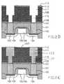
- FIG. 2Eis a cross-sectional view of the semiconductor device comprised of an illustrative MOS structure and a porous material layer 108 according to one illustrative embodiment of the present invention.
- the openings 110 , 111are filled with a conductive material, such as a metal, e.g., copper, aluminum, or tungsten, to form conductive contacts 131 , and conductive wiring lines 133 .
- the metalmay be deposited by a variety of methods, including a CVD process, plating, a combination of sputtering and subsequent metal-reflow, etc.
- planar surface 143 of the metallization layermay form the basis for subsequent metallization layers.
- the porous material layers 108may be fabricated separately and possibly in advance so that they can be stacked and connected in accordance with the specific design requirements. Furthermore, according to one embodiment of the present invention, a large portion of the entire dielectric material separating the MOS structure and the corresponding contacts 131 and wiring lines 133 , i.e., the dielectric layer 101 and the porous material layer 108 , consists of material having a low dielectric constant.
- the porosity of the porous material layer 108 comprised of, for example, siliconis adjusted so as to result in a dielectric constant being approximately the same as the dielectric constant of air, i.e., about one, thereby reducing the dielectric constant of the insulating material within the metallization layer compared to a conventional metallization layer by about 50%.
- a reduction of the stray capacitance of the wiring lines 133 of about 50%can be achieved, since the capacitance is proportional to the dielectric constant.
- the overall power consumption of the integrated circuitis also reduced as the current required for charging and discharging the stray capacitance is lower.
- the signal rise and fall timesare shorter due to the reduced RC time constant of the metallization layer.
- the present inventionprovides a semiconductor device in which a portion of the insulating area of the metallization layer exhibits a lower dielectric constant than metallization layers in conventional devices.
- a porous material layer 108comprised of materials such as any type of semiconducting material, dielectrics (glass, semiconductor oxides, etc.), which are suitable with respect to their dielectric constant and their properties of process handling.
- the degree of porosity of the porous material layer 108the dielectric constant of the layer can be adjusted close to the dielectric constant of air. Accordingly, the stray capacitance of the metallization layer is reduced, thereby improving the electrical characteristics of the device.
- the present inventionprovides a method for fabricating a semiconductor device having the features outlined above.
- the formation of a porous material layer 108 within a metallization layermay be performed separately from the formation of the product wafer 130 on a second substrate.
- the present inventionallows the formation of the metallization layer, i.e., the formation of openings for contacts and wiring lines according to standard processing techniques, either on the product wafer 130 after the porous material layer 108 is formed on the product wafer 130 , after the porous material layer 108 is transferred to the product wafer 130 , or separately formed in the porous material layer 108 , which, when completed, is then transferred to the product wafer 130 .
Landscapes
- Engineering & Computer Science (AREA)
- Physics & Mathematics (AREA)
- Condensed Matter Physics & Semiconductors (AREA)
- General Physics & Mathematics (AREA)
- Computer Hardware Design (AREA)
- Microelectronics & Electronic Packaging (AREA)
- Power Engineering (AREA)
- Manufacturing & Machinery (AREA)
- Internal Circuitry In Semiconductor Integrated Circuit Devices (AREA)
Abstract
Description
Claims (17)
Priority Applications (6)
| Application Number | Priority Date | Filing Date | Title |
|---|---|---|---|
| US09/475,572US6541863B1 (en) | 2000-01-05 | 2000-01-05 | Semiconductor device having a reduced signal processing time and a method of fabricating the same |
| KR1020027008757AKR100698495B1 (en) | 2000-01-05 | 2000-07-31 | Semiconductor device having reduced signal processing time and manufacturing method thereof |
| DE60037599TDE60037599T2 (en) | 2000-01-05 | 2000-07-31 | MANUFACTURING METHOD FOR SEMICONDUCTOR ARRANGEMENT WITH REDUCED SIGNAL WAY DELAY TIME |
| JP2001550807AJP2003519924A (en) | 2000-01-05 | 2000-07-31 | Semiconductor device having reduced signal processing time and method of manufacturing the same |
| EP00952341AEP1245045B1 (en) | 2000-01-05 | 2000-07-31 | A method of fabricating a semiconductor device having a reduced signal processing time |
| PCT/US2000/020886WO2001050527A1 (en) | 2000-01-05 | 2000-07-31 | A semiconductor device having a reduced signal processing time and a method of fabricating the same |
Applications Claiming Priority (1)
| Application Number | Priority Date | Filing Date | Title |
|---|---|---|---|
| US09/475,572US6541863B1 (en) | 2000-01-05 | 2000-01-05 | Semiconductor device having a reduced signal processing time and a method of fabricating the same |
Related Parent Applications (1)
| Application Number | Title | Priority Date | Filing Date |
|---|---|---|---|
| US09/454,695Continuation-In-PartUS6471603B1 (en) | 1996-10-23 | 1999-12-03 | Contoured golf club face |
Related Child Applications (1)
| Application Number | Title | Priority Date | Filing Date |
|---|---|---|---|
| US09/683,057Continuation-In-PartUS6569033B2 (en) | 1996-10-23 | 2001-11-13 | Striking plate for a golf club head |
Publications (1)
| Publication Number | Publication Date |
|---|---|
| US6541863B1true US6541863B1 (en) | 2003-04-01 |
Family
ID=23888165
Family Applications (1)
| Application Number | Title | Priority Date | Filing Date |
|---|---|---|---|
| US09/475,572Expired - LifetimeUS6541863B1 (en) | 2000-01-05 | 2000-01-05 | Semiconductor device having a reduced signal processing time and a method of fabricating the same |
Country Status (6)
| Country | Link |
|---|---|
| US (1) | US6541863B1 (en) |
| EP (1) | EP1245045B1 (en) |
| JP (1) | JP2003519924A (en) |
| KR (1) | KR100698495B1 (en) |
| DE (1) | DE60037599T2 (en) |
| WO (1) | WO2001050527A1 (en) |
Cited By (12)
| Publication number | Priority date | Publication date | Assignee | Title |
|---|---|---|---|---|
| US20020117686A1 (en)* | 2000-02-22 | 2002-08-29 | Samsung Electronics Co., Ltd. | Semiconductor device wiring and method of manufacturing the same |
| US20030227062A1 (en)* | 2002-06-07 | 2003-12-11 | Masatada Horiuchi | Semiconductor device and method of fabricating the same |
| US20030230779A1 (en)* | 2002-06-18 | 2003-12-18 | Park Yong-Jik | Semiconductor device and method for manufacturing the same |
| US20040150023A1 (en)* | 2001-06-29 | 2004-08-05 | Jian Li | Low-voltage and interface damage-free polymer memory device |
| US20060114850A1 (en)* | 2004-01-13 | 2006-06-01 | Joshi Avinash | System and method for achieving continuous connectivity to an access point or gateway in a wireless network following an on-demand routing protocol, and to perform smooth handoff of mobile terminals between fixed terminals in the network |
| US20060237800A1 (en)* | 2002-03-11 | 2006-10-26 | Micron Technology, Inc. | Semiconductor contact device |
| US7230336B2 (en)* | 2001-03-23 | 2007-06-12 | International Business Machines Corporation | Dual damascene copper interconnect to a damascene tungsten wiring level |
| US20080290421A1 (en)* | 2007-05-25 | 2008-11-27 | Ching-Ya Wang | Contact barrier structure and manufacturing methods |
| US8633520B2 (en) | 2010-10-21 | 2014-01-21 | Samsung Electronics Co., Ltd. | Semiconductor device |
| US10096549B2 (en)* | 2016-09-12 | 2018-10-09 | Samsung Electronics Co., Ltd. | Semiconductor devices having interconnection structure |
| US10643926B2 (en)* | 2017-12-22 | 2020-05-05 | Samsung Electronics Co., Ltd. | Semiconductor device having a structure for insulating layer under metal line |
| US11804376B2 (en)* | 2019-07-18 | 2023-10-31 | Tokyo Electron Limited | Method for mitigating lateral film growth in area selective deposition |
Families Citing this family (1)
| Publication number | Priority date | Publication date | Assignee | Title |
|---|---|---|---|---|
| US7834456B2 (en)* | 2009-01-20 | 2010-11-16 | Raytheon Company | Electrical contacts for CMOS devices and III-V devices formed on a silicon substrate |
Citations (20)
| Publication number | Priority date | Publication date | Assignee | Title |
|---|---|---|---|---|
| US4380865A (en)* | 1981-11-13 | 1983-04-26 | Bell Telephone Laboratories, Incorporated | Method of forming dielectrically isolated silicon semiconductor materials utilizing porous silicon formation |
| US4628591A (en)* | 1984-10-31 | 1986-12-16 | Texas Instruments Incorporated | Method for obtaining full oxide isolation of epitaxial islands in silicon utilizing selective oxidation of porous silicon |
| US4866009A (en)* | 1986-11-17 | 1989-09-12 | Kabushiki Kaisha Toshiba | Multilayer wiring technique for a semiconductor device |
| EP0333132A2 (en) | 1988-03-15 | 1989-09-20 | Nec Corporation | Semiconductor device having multilayered wiring structure with a small parasitic capacitance |
| US5494858A (en)* | 1994-06-07 | 1996-02-27 | Texas Instruments Incorporated | Method for forming porous composites as a low dielectric constant layer with varying porosity distribution electronics applications |
| US5691238A (en) | 1995-06-07 | 1997-11-25 | Advanced Micro Devices, Inc. | Subtractive dual damascene |
| WO1998000862A1 (en) | 1996-06-28 | 1998-01-08 | Advanced Micro Devices, Inc. | Solid porous insulated conductive lines |
| US5744865A (en)* | 1996-10-22 | 1998-04-28 | Texas Instruments Incorporated | Highly thermally conductive interconnect structure for intergrated circuits |
| US5821621A (en)* | 1995-10-12 | 1998-10-13 | Texas Instruments Incorporated | Low capacitance interconnect structure for integrated circuits |
| US5847443A (en) | 1994-06-23 | 1998-12-08 | Texas Instruments Incorporated | Porous dielectric material with improved pore surface properties for electronics applications |
| US5870076A (en) | 1994-11-11 | 1999-02-09 | Daewoo Electronics, Co., Ltd. | Pixel data correction apparatus for use with an actuated mirror array |
| US5904576A (en)* | 1996-11-01 | 1999-05-18 | Yamaha Corporation | Method of forming wiring structure |
| US5914183A (en)* | 1993-12-06 | 1999-06-22 | The Secretary Of State For Defence In Her Brittanic Majesty's Government Of The United Kingdom Of Great Britain And Northern Ireland | Porous semiconductor material |
| US6017811A (en)* | 1993-09-09 | 2000-01-25 | The United States Of America As Represented By The Secretary Of The Navy | Method of making improved electrical contact to porous silicon |
| US6037634A (en)* | 1996-02-02 | 2000-03-14 | Mitsubishi Denki Kabushiki Kaisha | Semiconductor device with first and second elements formed on first and second portions |
| US6090724A (en)* | 1998-12-15 | 2000-07-18 | Lsi Logic Corporation | Method for composing a thermally conductive thin film having a low dielectric property |
| US6265303B1 (en)* | 1997-05-28 | 2001-07-24 | Texas Instruments Incorporated | Integrated circuit dielectric and method |
| US6287936B1 (en)* | 1998-05-19 | 2001-09-11 | Stmicroelectronics S.A. | Method of forming porous silicon in a silicon substrate, in particular for improving the performance of an inductive circuit |
| US6376859B1 (en)* | 1998-07-29 | 2002-04-23 | Texas Instruments Incorporated | Variable porosity porous silicon isolation |
| US6407441B1 (en)* | 1997-12-29 | 2002-06-18 | Texas Instruments Incorporated | Integrated circuit and method of using porous silicon to achieve component isolation in radio frequency applications |
Family Cites Families (3)
| Publication number | Priority date | Publication date | Assignee | Title |
|---|---|---|---|---|
| JPH08125016A (en)* | 1994-10-24 | 1996-05-17 | Sony Corp | Manufacture of semiconductor device |
| KR100311880B1 (en)* | 1996-11-11 | 2001-12-20 | 미다라이 후지오 | Method of producing a through-hole, silicon substrate having a through-hole, device using such a substrate, method of producing an ink-jet print head, and ink-jet print head |
| JPH11312733A (en)* | 1998-04-28 | 1999-11-09 | Nkk Corp | Manufacturing method of integrated circuit device |
- 2000
- 2000-01-05USUS09/475,572patent/US6541863B1/ennot_activeExpired - Lifetime
- 2000-07-31DEDE60037599Tpatent/DE60037599T2/ennot_activeExpired - Lifetime
- 2000-07-31KRKR1020027008757Apatent/KR100698495B1/ennot_activeExpired - Fee Related
- 2000-07-31JPJP2001550807Apatent/JP2003519924A/enactivePending
- 2000-07-31WOPCT/US2000/020886patent/WO2001050527A1/enactiveIP Right Grant
- 2000-07-31EPEP00952341Apatent/EP1245045B1/ennot_activeExpired - Lifetime
Patent Citations (22)
| Publication number | Priority date | Publication date | Assignee | Title |
|---|---|---|---|---|
| US4380865A (en)* | 1981-11-13 | 1983-04-26 | Bell Telephone Laboratories, Incorporated | Method of forming dielectrically isolated silicon semiconductor materials utilizing porous silicon formation |
| US4628591A (en)* | 1984-10-31 | 1986-12-16 | Texas Instruments Incorporated | Method for obtaining full oxide isolation of epitaxial islands in silicon utilizing selective oxidation of porous silicon |
| US4866009A (en)* | 1986-11-17 | 1989-09-12 | Kabushiki Kaisha Toshiba | Multilayer wiring technique for a semiconductor device |
| EP0333132A2 (en) | 1988-03-15 | 1989-09-20 | Nec Corporation | Semiconductor device having multilayered wiring structure with a small parasitic capacitance |
| US5103288A (en)* | 1988-03-15 | 1992-04-07 | Nec Corporation | Semiconductor device having multilayered wiring structure with a small parasitic capacitance |
| US6017811A (en)* | 1993-09-09 | 2000-01-25 | The United States Of America As Represented By The Secretary Of The Navy | Method of making improved electrical contact to porous silicon |
| US5914183A (en)* | 1993-12-06 | 1999-06-22 | The Secretary Of State For Defence In Her Brittanic Majesty's Government Of The United Kingdom Of Great Britain And Northern Ireland | Porous semiconductor material |
| US5494858A (en)* | 1994-06-07 | 1996-02-27 | Texas Instruments Incorporated | Method for forming porous composites as a low dielectric constant layer with varying porosity distribution electronics applications |
| US5561318A (en) | 1994-06-07 | 1996-10-01 | Texas Instruments Incorporated | Porous composites as a low dielectric constant material for electronics applications |
| US5847443A (en) | 1994-06-23 | 1998-12-08 | Texas Instruments Incorporated | Porous dielectric material with improved pore surface properties for electronics applications |
| US5870076A (en) | 1994-11-11 | 1999-02-09 | Daewoo Electronics, Co., Ltd. | Pixel data correction apparatus for use with an actuated mirror array |
| US5691238A (en) | 1995-06-07 | 1997-11-25 | Advanced Micro Devices, Inc. | Subtractive dual damascene |
| US5821621A (en)* | 1995-10-12 | 1998-10-13 | Texas Instruments Incorporated | Low capacitance interconnect structure for integrated circuits |
| US6037634A (en)* | 1996-02-02 | 2000-03-14 | Mitsubishi Denki Kabushiki Kaisha | Semiconductor device with first and second elements formed on first and second portions |
| WO1998000862A1 (en) | 1996-06-28 | 1998-01-08 | Advanced Micro Devices, Inc. | Solid porous insulated conductive lines |
| US5744865A (en)* | 1996-10-22 | 1998-04-28 | Texas Instruments Incorporated | Highly thermally conductive interconnect structure for intergrated circuits |
| US5904576A (en)* | 1996-11-01 | 1999-05-18 | Yamaha Corporation | Method of forming wiring structure |
| US6265303B1 (en)* | 1997-05-28 | 2001-07-24 | Texas Instruments Incorporated | Integrated circuit dielectric and method |
| US6407441B1 (en)* | 1997-12-29 | 2002-06-18 | Texas Instruments Incorporated | Integrated circuit and method of using porous silicon to achieve component isolation in radio frequency applications |
| US6287936B1 (en)* | 1998-05-19 | 2001-09-11 | Stmicroelectronics S.A. | Method of forming porous silicon in a silicon substrate, in particular for improving the performance of an inductive circuit |
| US6376859B1 (en)* | 1998-07-29 | 2002-04-23 | Texas Instruments Incorporated | Variable porosity porous silicon isolation |
| US6090724A (en)* | 1998-12-15 | 2000-07-18 | Lsi Logic Corporation | Method for composing a thermally conductive thin film having a low dielectric property |
Non-Patent Citations (1)
| Title |
|---|
| Poponiak et.al. "High Sheet Resistivity Resistors by the Porous Silicon", Jun. 1975, IBM Tech Disclosure Bulletiin.* |
Cited By (20)
| Publication number | Priority date | Publication date | Assignee | Title |
|---|---|---|---|---|
| US20020117686A1 (en)* | 2000-02-22 | 2002-08-29 | Samsung Electronics Co., Ltd. | Semiconductor device wiring and method of manufacturing the same |
| US7012335B2 (en)* | 2000-02-22 | 2006-03-14 | Samsung Electronics Co., Ltd. | Semiconductor device wiring and method of manufacturing the same |
| US7230336B2 (en)* | 2001-03-23 | 2007-06-12 | International Business Machines Corporation | Dual damascene copper interconnect to a damascene tungsten wiring level |
| US6952017B2 (en)* | 2001-06-29 | 2005-10-04 | Intel Corporation | Low-voltage and interface damage-free polymer memory device |
| US20040150023A1 (en)* | 2001-06-29 | 2004-08-05 | Jian Li | Low-voltage and interface damage-free polymer memory device |
| US20060237800A1 (en)* | 2002-03-11 | 2006-10-26 | Micron Technology, Inc. | Semiconductor contact device |
| US7932557B2 (en)* | 2002-03-11 | 2011-04-26 | Micron Technology, Inc. | Semiconductor contact device |
| US20030227062A1 (en)* | 2002-06-07 | 2003-12-11 | Masatada Horiuchi | Semiconductor device and method of fabricating the same |
| US20050064640A1 (en)* | 2002-06-18 | 2005-03-24 | Samsung Electronics Co.Ltd. | Semiconductor device and method for manufacturing the same |
| US20030230779A1 (en)* | 2002-06-18 | 2003-12-18 | Park Yong-Jik | Semiconductor device and method for manufacturing the same |
| US7091072B2 (en) | 2002-06-18 | 2006-08-15 | Samsung Electronics Co., Ltd. | Semiconductor device and method for manufacturing the same |
| US20060114850A1 (en)* | 2004-01-13 | 2006-06-01 | Joshi Avinash | System and method for achieving continuous connectivity to an access point or gateway in a wireless network following an on-demand routing protocol, and to perform smooth handoff of mobile terminals between fixed terminals in the network |
| US7709903B2 (en)* | 2007-05-25 | 2010-05-04 | Taiwan Semiconductor Manufacturing Company, Ltd. | Contact barrier structure and manufacturing methods |
| US20100167485A1 (en)* | 2007-05-25 | 2010-07-01 | Taiwan Semiconductor Manufacturing Company, Ltd. | Contact Barrier Structure and Manufacturing Methods |
| US20080290421A1 (en)* | 2007-05-25 | 2008-11-27 | Ching-Ya Wang | Contact barrier structure and manufacturing methods |
| US8030210B2 (en) | 2007-05-25 | 2011-10-04 | Taiwan Semiconductor Manufacturing Company, Ltd. | Contact barrier structure and manufacturing methods |
| US8633520B2 (en) | 2010-10-21 | 2014-01-21 | Samsung Electronics Co., Ltd. | Semiconductor device |
| US10096549B2 (en)* | 2016-09-12 | 2018-10-09 | Samsung Electronics Co., Ltd. | Semiconductor devices having interconnection structure |
| US10643926B2 (en)* | 2017-12-22 | 2020-05-05 | Samsung Electronics Co., Ltd. | Semiconductor device having a structure for insulating layer under metal line |
| US11804376B2 (en)* | 2019-07-18 | 2023-10-31 | Tokyo Electron Limited | Method for mitigating lateral film growth in area selective deposition |
Also Published As
| Publication number | Publication date |
|---|---|
| EP1245045B1 (en) | 2007-12-26 |
| WO2001050527A1 (en) | 2001-07-12 |
| DE60037599D1 (en) | 2008-02-07 |
| KR20020065641A (en) | 2002-08-13 |
| DE60037599T2 (en) | 2008-04-30 |
| EP1245045A1 (en) | 2002-10-02 |
| JP2003519924A (en) | 2003-06-24 |
| KR100698495B1 (en) | 2007-03-23 |
Similar Documents
| Publication | Publication Date | Title |
|---|---|---|
| KR101742925B1 (en) | Structure and formation method of damascene structure | |
| TWI686880B (en) | Semiconductor device and methods of fabrication thereof | |
| US6232237B1 (en) | Method for fabricating semiconductor device | |
| US6329279B1 (en) | Method of fabricating metal interconnect structure having outer air spacer | |
| US20210313416A1 (en) | Structure and formation method of semiconductor device with capacitors | |
| US10586733B2 (en) | Multi-level air gap formation in dual-damascene structure | |
| US7651942B2 (en) | Metal interconnect structure and method | |
| US9685497B2 (en) | Embedded metal-insulator-metal capacitor | |
| WO2006078815A2 (en) | Single mask mim capacitor and resistor with in trench copper drift barrier | |
| CN103811414B (en) | Copper etching integrated approach | |
| US6541863B1 (en) | Semiconductor device having a reduced signal processing time and a method of fabricating the same | |
| CN109804463B (en) | Method for forming a dual damascene interconnect structure | |
| US20070040188A1 (en) | Contact or via hole structure with enlarged bottom critical dimension | |
| US20070210339A1 (en) | Shared contact structures for integrated circuits | |
| US6680542B1 (en) | Damascene structure having a metal-oxide-metal capacitor associated therewith | |
| CN113314461A (en) | Method for an interconnection scheme | |
| US11158536B2 (en) | Patterning line cuts before line patterning using sacrificial fill material | |
| US7115467B2 (en) | Metal insulator metal (MIM) capacitor fabrication with sidewall barrier removal aspect | |
| CN107180785A (en) | Method for forming semiconductor device structure | |
| US6153933A (en) | Elimination of residual materials in a multiple-layer interconnect structure | |
| US6656825B2 (en) | Semiconductor device having an improved local interconnect structure and a method for forming such a device | |
| US7112537B2 (en) | Method of fabricating interconnection structure of semiconductor device | |
| US9202758B1 (en) | Method for manufacturing a contact for a semiconductor component and related structure | |
| US20020119618A1 (en) | Method for forming contacts of memory devices using an etch stop layer | |
| US6750544B1 (en) | Metallization system for use in a semiconductor component |
Legal Events
| Date | Code | Title | Description |
|---|---|---|---|
| AS | Assignment | Owner name:ADVANCED MICRO DEVICES, INC., TEXAS Free format text:ASSIGNMENT OF ASSIGNORS INTEREST;ASSIGNORS:HORSTMANN, MANFRED;WIECZOREK, KARSTEN;BURBACH, GERT;REEL/FRAME:010535/0142;SIGNING DATES FROM 19991110 TO 19991111 | |
| STCF | Information on status: patent grant | Free format text:PATENTED CASE | |
| FPAY | Fee payment | Year of fee payment:4 | |
| AS | Assignment | Owner name:GLOBALFOUNDRIES INC., CAYMAN ISLANDS Free format text:AFFIRMATION OF PATENT ASSIGNMENT;ASSIGNOR:ADVANCED MICRO DEVICES, INC.;REEL/FRAME:023119/0083 Effective date:20090630 | |
| FPAY | Fee payment | Year of fee payment:8 | |
| FPAY | Fee payment | Year of fee payment:12 | |
| AS | Assignment | Owner name:WILMINGTON TRUST, NATIONAL ASSOCIATION, DELAWARE Free format text:SECURITY AGREEMENT;ASSIGNOR:GLOBALFOUNDRIES INC.;REEL/FRAME:049490/0001 Effective date:20181127 | |
| AS | Assignment | Owner name:GLOBALFOUNDRIES INC., CAYMAN ISLANDS Free format text:RELEASE BY SECURED PARTY;ASSIGNOR:WILMINGTON TRUST, NATIONAL ASSOCIATION;REEL/FRAME:054636/0001 Effective date:20201117 | |
| AS | Assignment | Owner name:GLOBALFOUNDRIES U.S. INC., NEW YORK Free format text:RELEASE BY SECURED PARTY;ASSIGNOR:WILMINGTON TRUST, NATIONAL ASSOCIATION;REEL/FRAME:056987/0001 Effective date:20201117 |