US6541816B2 - Planar structure for non-volatile memory devices - Google Patents
Planar structure for non-volatile memory devicesDownload PDFInfo
- Publication number
- US6541816B2 US6541816B2US09/893,026US89302601AUS6541816B2US 6541816 B2US6541816 B2US 6541816B2US 89302601 AUS89302601 AUS 89302601AUS 6541816 B2US6541816 B2US 6541816B2
- Authority
- US
- United States
- Prior art keywords
- dielectric
- oxide
- charge trapping
- core region
- memory device
- Prior art date
- Legal status (The legal status is an assumption and is not a legal conclusion. Google has not performed a legal analysis and makes no representation as to the accuracy of the status listed.)
- Expired - Fee Related
Links
Images


Classifications
- H—ELECTRICITY
- H10—SEMICONDUCTOR DEVICES; ELECTRIC SOLID-STATE DEVICES NOT OTHERWISE PROVIDED FOR
- H10B—ELECTRONIC MEMORY DEVICES
- H10B43/00—EEPROM devices comprising charge-trapping gate insulators
- H10B43/30—EEPROM devices comprising charge-trapping gate insulators characterised by the memory core region
- H—ELECTRICITY
- H10—SEMICONDUCTOR DEVICES; ELECTRIC SOLID-STATE DEVICES NOT OTHERWISE PROVIDED FOR
- H10B—ELECTRONIC MEMORY DEVICES
- H10B43/00—EEPROM devices comprising charge-trapping gate insulators
- H10B43/40—EEPROM devices comprising charge-trapping gate insulators characterised by the peripheral circuit region
- H—ELECTRICITY
- H10—SEMICONDUCTOR DEVICES; ELECTRIC SOLID-STATE DEVICES NOT OTHERWISE PROVIDED FOR
- H10B—ELECTRONIC MEMORY DEVICES
- H10B69/00—Erasable-and-programmable ROM [EPROM] devices not provided for in groups H10B41/00 - H10B63/00, e.g. ultraviolet erasable-and-programmable ROM [UVEPROM] devices
- Y—GENERAL TAGGING OF NEW TECHNOLOGICAL DEVELOPMENTS; GENERAL TAGGING OF CROSS-SECTIONAL TECHNOLOGIES SPANNING OVER SEVERAL SECTIONS OF THE IPC; TECHNICAL SUBJECTS COVERED BY FORMER USPC CROSS-REFERENCE ART COLLECTIONS [XRACs] AND DIGESTS
- Y10—TECHNICAL SUBJECTS COVERED BY FORMER USPC
- Y10S—TECHNICAL SUBJECTS COVERED BY FORMER USPC CROSS-REFERENCE ART COLLECTIONS [XRACs] AND DIGESTS
- Y10S438/00—Semiconductor device manufacturing: process
- Y10S438/954—Making oxide-nitride-oxide device
- Y—GENERAL TAGGING OF NEW TECHNOLOGICAL DEVELOPMENTS; GENERAL TAGGING OF CROSS-SECTIONAL TECHNOLOGIES SPANNING OVER SEVERAL SECTIONS OF THE IPC; TECHNICAL SUBJECTS COVERED BY FORMER USPC CROSS-REFERENCE ART COLLECTIONS [XRACs] AND DIGESTS
- Y10—TECHNICAL SUBJECTS COVERED BY FORMER USPC
- Y10S—TECHNICAL SUBJECTS COVERED BY FORMER USPC CROSS-REFERENCE ART COLLECTIONS [XRACs] AND DIGESTS
- Y10S438/00—Semiconductor device manufacturing: process
- Y10S438/981—Utilizing varying dielectric thickness
Definitions
- the present inventiongenerally relates to nonvolatile memory devices.
- the present inventionrelates to SONOS type non-volatile memory devices having a substantially planar structure.
- EEPROMselectrically erasable programmable read only memory
- a memory cellcharacterized by a vertical stack of a tunnel oxide, a first polysilicon layer over the tunnel oxide, an ONO (oxide-nitride-oxide) interlevel dielectric over the first polysilicon layer, and a second polysilicon layer over the ONO interlevel dielectric.
- ONOoxide-nitride-oxide
- Guterman et alrelates to a floating gate nonvolatile memory cell consisting of a floating gate sandwiched between a gate oxide and an interlevel oxide, with a control gate over the interlevel oxide.
- a flash memory cellis programmed by inducing hot electron injection from a portion of the substrate, such as the channel section near the drain region, to the floating gate. Electron injection carries negative charge into the floating gate.
- the injection mechanismcan be induced by grounding the source region and a bulk portion of the substrate and applying a relatively high positive voltage to the control electrode to create an electron attracting field and applying a positive voltage of moderate magnitude to the drain region in order to generate “hot” (high energy) electrons.
- FETfloating effect transistor
- the magnitude of the read currentis used to determine whether or not a flash memory cell is programmed.
- the act of discharging the floating gate of a flash memory cellis called the erase function.
- the erase functionis typically carried out by a Fowler-Nordheim tunneling mechanism between the floating gate and the source region of the transistor (source erase or negative gate erase) or between the floating gate and the substrate (channel erase).
- a source erase operationis induced by applying a high positive voltage to the source region and a 0 V to the control gate and the substrate while floating the drain of the respective memory cell.
- SONOSSilicon Oxide Nitride Oxide Silicon
- flash memory cellsare constructed having a charge trapping non-conducting dielectric layer, typically a silicon nitride layer, sandwiched between two silicon dioxide layers (insulating layers).
- the nonconducting dielectric layerfunctions as an electrical charge trapping medium.
- a conducting gate layeris placed over the upper silicon dioxide layer. Since the electrical charge is trapped locally near whichever side that is used as the drain, this structure can be described as a two-transistor cell, or two-bits per cell. If multi-level is used, then four or more bits per cell can be accomplished.
- Multi-bit cellsenable SONOS type memory devices to have the advantage over others in facilitating the continuing trend increasing the amount of information held/processed on an integrated circuit chip.
- each bitis read in a direction opposite that in which it is programmed with a relatively low gate voltage.
- the right bitis programmed conventionally by applying programming voltages to the gate and the drain while the source is grounded or at a lower voltage. Hot electrons are accelerated sufficiently so that they are injected into a region of the trapping dielectric layer near the drain.
- the deviceis read in the opposite direction from which it is written, meaning voltages are applied to the gate and the source while the drain is grounded or at a lower voltage.
- the left bitis similarly programmed and read by swapping the functionality of source and drain terminals.
- Reading in the reverse directionis most effective when relatively low gate voltages are used.
- a benefit of utilizing relatively low gate voltages in combination with reading in the reverse directionis that the potential drop across the portion of the channel beneath the trapped charge region is significantly reduced.
- a relatively small programming region or charge trapping regionis possible due to the lower channel potential drop under the charge trapping region. This permits much faster programming times because the effect of the charge trapped in the localized trapping region is amplified. Programming times are reduced while the delta in threshold voltage between the programmed versus unprogrammed states remains the same as when the device is read in the forward direction.
- SONOS type memory devicesoffer additional advantages as well.
- the erase mechanism of the memory cellis greatly enhanced. Both bits of the memory cell can be erased by applying suitable erase voltages to the gate and the drain for the right bit and to the gate and the source for the left bit.
- Another advantageincludes reduced wearout from cycling thus increasing device longevity.
- An effect of reading in the reverse directionis that a much higher threshold voltage for the same amount of programming is possible.
- a much smaller region of trapped chargeis required when the cell is read in the reverse direction than when the cell is read in the forward direction.
- the erase mechanismis enhanced when the charge trapping region is made as narrow as possible. Programming in the forward direction and reading in the reverse direction permits limiting the width of the charge trapping region to a narrow region near the drain (right bit) or the source. This allows for much more efficient erasing of the memory cell.
- Another advantage of localized charge trappingis that during erase, the region of the nitride away from the drain does not experience deep depletion since the erase occurs near the drain only.
- the final threshold of the cell after erasingis self limited by the device structure itself. This is in direct contrast to conventional single transistor floating gate flash memory cells which often have deep depletion problems.
- LOCOSLOCal Oxidation of Silicon
- Isolation by LOCOSalso causes undesirable outgassing of dopants.
- LOCOS formationcauses short channeling. There are high temperatures associated with LOCOS formation, often from 800° C. to 1,100° C. Short channeling is a decrease in the effective channel length, often represented as L eff . Unnecessarily decreasing the effective channel length results in an undesirably large current passing through the transistor at low gate voltages such as when the transistor is in the “off” state.
- the SONOS type memory devicescan be formed in the following manner.
- EEPROM memory cellsare formed with buried bitlines.
- the buried bitlines and bitline oxidesare formed in the core region of the substrate prior to formation of the ONO dielectric.
- Mitchell et alforms EEPROM memory cells by forming an ONO dielectric, depositing polysilicon over the ONO dielectric, patterning the polysilicon, forming the buried bitlines, and removing the ONO dielectric covering the bitlines.
- an ONO dielectricis formed over the substrate, a bitline mask is patterned over the ONO dielectric in core while completely covering the periphery, portions of the top oxide and nitride layers left exposed by the bitline mask are etched/removed, the bitlines are implanted, then bitline oxides are formed over the bitlines.
- memory cellsare formed by forming an ONO dielectric, a bitline mask with openings for the bitlines is formed over the ONO dielectric, the top oxide and nitride layers left exposed by the bitline mask are etched/removed, the bitlines are implanted, the bitline mask is removed, the exposed portions of the bottom oxide of the ONO dielectric are removed, gate oxides are grown including thick oxide growth over the bitlines, and polysilicon gates and wordlines are formed.
- the present inventionprovides non-volatile semiconductor memory devices having a substantially planar structure.
- the present inventionrelates to a simplified process for fabricating substantially planar SONOS type nonvolatile memory devices, and in particular, a simplified process for forming buried bitlines in SONOS type nonvolatile memory devices.
- the SONOS type nonvolatile memory deviceslead to the efficient production of dense, robust single-poly devices, having a substantially planar structure.
- the present inventionprovides a substantially planar structure and eliminates the need for a core region etch step thus reducing costs and defect formation. There are a number of benefits associated with the generally flat topography of the memory devices.
- the present inventioneliminates high temperature thermal cycling associated with LOCOS formation in the core region, thereby minimizing and/or eliminating short channeling.
- the present inventionalso eliminates undesirable bird's beak associated with LOCOS formation which may lead to fewer defects and/or improved scaling.
- Another advantageis that in some instances the bitline implant does not experience the periphery gate oxide thermal cycle.
- One aspect of the present inventionrelates to a non-volatile semiconductor memory device, containing a substrate, the substrate having a core region and a periphery region; a charge trapping dielectric over the core region of the substrate; a gate dielectric in the periphery region of the substrate; buried bitlines under the charge trapping dielectric in the core region; and wordlines over the charge trapping dielectric in the core region, wherein the core region is substantially planar.
- FIG. 1illustrates a cross-sectional view of one aspect of a method in accordance with the present invention.
- FIG. 2illustrates a cross-sectional view of another aspect of a method in accordance with the present invention.
- FIG. 3illustrates a cross-sectional view of yet another aspect of a method in accordance with the present invention.
- FIG. 4illustrates a cross-sectional view of still yet another aspect of a method in accordance with the present invention.
- FIG. 5illustrates a cross-sectional view of another aspect of a method in accordance with the present invention.
- FIG. 6illustrates a cross-sectional view of a SONOS type memory cell in accordance with one aspect of the invention.
- FIG. 7illustrates a cross-sectional view of one aspect of another method in accordance with the present invention.
- FIG. 8illustrates a cross-sectional view of another aspect of another method in accordance with the present invention.
- FIG. 9illustrates a cross-sectional view of yet another aspect of another method in accordance with the present invention.
- FIG. 10illustrates a cross-sectional view of still yet another aspect of another method in accordance with the present invention.
- FIG. 11illustrates a cross-sectional view of another aspect of another method in accordance with the present invention.
- FIG. 12illustrates a cross-sectional view of a SONOS type memory cell in accordance with another aspect of the invention.
- FIG. 13illustrates a cross-sectional view of one aspect of yet another method in accordance with the present invention.
- FIG. 14illustrates a cross-sectional view of another aspect of yet another method in accordance with the present invention.
- FIG. 15illustrates a cross-sectional view of yet another aspect of yet another method in accordance with the present invention.
- FIG. 16illustrates a cross-sectional view of still yet another aspect of yet another method in accordance with the present invention.
- FIG. 17illustrates a cross-sectional view of another aspect of yet another method in accordance with the present invention.
- FIG. 18illustrates a cross-sectional view of another aspect of yet another method in accordance with the present invention.
- FIG. 19illustrates a cross-sectional view of a SONOS type memory cell in accordance with yet another aspect of the invention.
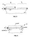
- FIG. 20illustrates a perspective view of the core region of a SONOS type memory device in accordance with one aspect of the invention.
- FIG. 21illustrates a perspective view of the core region of another SONOS type memory device in accordance with one aspect of the invention.
- FIG. 22illustrates a perspective view of the core region of a prior art SONOS type memory device.
- the present inventioninvolves a substantially planar SONOS type nonvolatile memory devices.
- the SONOS type memory cells of an arrayare coupled to wordlines and bitlines.
- the drains and the sources of the SONOS type memory cellsare connected to the bitlines.
- peripheral decoders and control circuitryeach memory cell can be addressed for programming, reading or erasing functions. Formation of bitlines is therefore necessary to the operation of the SONOS type nonvolatile memory devices.
- One aspect of the present inventioninvolves providing substantially planar non-volatile semiconductor memory devices that do not contain LOCOS in the core region. As a result, undesirable bird's beak and high temperature thermal cycling associated with LOCOS formation is minimized and/or eliminated.
- the planar structure of the corepermits the reliable formation of additional layers and structures thereover that are necessary to complete the fabrication of the non-volatile semiconductor memory devices. Handling and packaging non-volatile semiconductor memory devices having substantially planar core regions is typically easier and more efficient than memory devices that do not have planar core regions.
- the less severe topography of the non-volatile semiconductor memory devices of the present inventioncontributes to improved linewidth control (more uniform linewidths) as well as improved junctions (controlled diffusion).
- Substantially planardoes not require absolute planarity.
- Substantially planarmeans the absence of severe variations in surface height.
- a substantially planar surfacethere may exist mesas, peaks, and valleys that do not vary (from the top of a peak to the bottom of a valley) by more than about 250 ⁇ .
- a substantially planar surfacethere may exist mesas, peaks, and valleys that do not vary by more than about 200 ⁇ .
- a substantially planar surfacethere may exist mesas, peaks, and valleys that do not vary by more than about 100 ⁇ .
- Substantially planarmay alternatively mean that the wordlines are substantially uniform in thickness across the core region and simultaneously generally planar.
- the structure of FIG. 20is substantially planar (although it is not absolutely planar) whereas the structure of FIG. 22 is not substantially planar.
- a method of forming a substantially planar non-volatile semiconductor memory deviceinvolves the sequential or non-sequential steps of forming a charge trapping dielectric over a substrate, the substrate having a core region and a periphery region; removing at least a portion of the charge trapping dielectric in the periphery region; forming a gate dielectric in the periphery region; forming buried bitlines in the core region; and forming gates in the core region and the periphery region.
- Another method of forming a substantially planar non-volatile semiconductor memory deviceinvolves the steps of forming a charge trapping dielectric over a substrate, the substrate having a core region and a periphery region; removing at least a portion of the charge trapping dielectric in the periphery region; forming a gate dielectric in the periphery region; forming buried bitlines in the core region; and forming gates in the core region and the periphery region.
- Yet another method of forming a substantially planar non-volatile semiconductor memory deviceinvolves the steps of forming a charge trapping dielectric over a substrate, the substrate having a core region and a periphery region; forming buried bitlines in the core region; removing at least a portion of the charge trapping dielectric in the periphery region; forming a gate dielectric in the periphery region; and forming gates in the core region and the periphery region.
- Still yet another method of forming a substantially planar non-volatile semiconductor memory deviceinvolves the steps of forming a charge trapping dielectric over a substrate, the substrate having a core region and a periphery region; removing at least a portion of the charge trapping dielectric in the periphery region; forming a gate dielectric having a first thickness in the periphery region; forming buried bitlines in the core region; increasing the thickness of the gate dielectric in at least a portion of the periphery region to provide a gate dielectric having a second thickness; and forming gates in the core region and the periphery region.
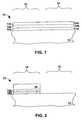
- FIGS. 1-6One aspect of the present invention is described in FIGS. 1-6.
- a semiconductor structure 10is shown with a semiconductor substrate 12 under a charge trapping dielectric 14 .
- Semiconductor structure 10contains two regions, the core region 16 containing the memory cells and the periphery region 18 containing the rest of the chip such as the controlling logic and input/output devices.
- the charge trapping dielectric 14contains three layers; namely, a first silicon dioxide layer 14 a, a silicon nitride layer 14 b, and a second silicon dioxide layer 14 c (an ONO dielectric). Particularly in the case of an ONO dielectric, the electron trapping is in the silicon nitride layer 14 b.
- a SONOS type nonvolatile memory devicemay contain any of the charge trapping dielectrics described above.
- a SONOS type nonvolatile memory devicecontains any dielectric layer or layers that are capable of or facilitate electron trapping, and the SONOS type nonvolatile memory device contains an ONO charge trapping dielectric only when a specific reference to such dielectric is indicated.
- one or both of the silicon dioxide layers 14 a and 14 cmay be a silicon-rich silicon dioxide layer.
- One or both of the silicon dioxide layers 14 a and 14 cmay also be an oxygen-rich silicon dioxide layer.
- One or both of the silicon dioxide layers 14 a and 14 cmay be a thermally grown or a deposited oxide.
- One or both of the silicon dioxide layers 14 a and 14 cmay be nitrided oxide layers.
- the nitride 14 bmay be a silicon-rich silicon nitride layer.
- the nitride 14 bmay also be an nitrogen-rich silicon nitride layer.
- the charge trapping dielectric 14has a thickness from about 75 ⁇ to about 300 ⁇ . In another embodiment, the charge trapping dielectric 14 has a thickness from about 100 ⁇ to about 275 ⁇ . In yet another embodiment, the charge trapping dielectric 14 has a thickness from about 110 ⁇ to about 250 ⁇ .
- the oxide layers 14 a and 14 cindividually have thicknesses from about 50 ⁇ to about 150 ⁇ while the nitride layer 14 b has a thickness from about 20 ⁇ to about 80 ⁇ . In another embodiment, the oxide layers 14 a and 14 c individually have thicknesses from about 60 ⁇ to about 140 ⁇ while the nitride layer 14 b has a thickness from about 25 ⁇ to about 75 ⁇ . In yet another embodiment, the oxide layers 14 a and 14 c individually have thicknesses from about 70 ⁇ to about 130 ⁇ while the nitride layer 14 b has a thickness from about 30 ⁇ to about 70 ⁇ .
- a mask such as a suitable photoresist 20is used to cover the charge trapping dielectric 14 in the core region 16 leaving the charge trapping dielectric 14 exposed in the periphery region 18 of the structure 10 .
- the charge trapping dielectric 14 exposed in the periphery region 18is etched down to the substrate 12 (the first silicon dioxide layer 14 a, the silicon nitride layer 14 b, and the second silicon dioxide layer 14 c are removed in the periphery region 18 of the structure 10 ). Multiple etching steps may be employed to remove the charge trapping dielectric 14 .
- a gate dielectric 22such as an oxide layer is provided using any suitable means, such as chemical vapor deposition (CVD), dry oxidation, wet oxidation or rapid thermal oxidation, on at least a portion of the exposed portions of the substrate 12 (over the periphery region 18 ). Dry oxidation, wet oxidation, and rapid thermal oxidation are preferred, especially when gate dielectric 22 contains silicon dioxide. CVD techniques are employed in instances where the gate dielectric 22 contains one or more of silicon dioxide, silicon nitride, and silicon oxynitride.
- CVDchemical vapor deposition
- the gate dielectric 22later serves as the gate dielectric for subsequently formed high and/or low voltage transistors (not shown) in the periphery region 18 .
- the gate dielectric 22has a thickness from about 30 ⁇ to about 300 ⁇ . In another embodiment, the gate dielectric 22 has a thickness from about 40 ⁇ to about 250 ⁇ .
- photoresist 20is stripped or removed from the semiconductor structure 10 .
- another masksuch as a suitable photoresist 24 is used to partially cover the charge trapping dielectric 14 in the core region 16 while covering the gate dielectric 22 in the periphery region 18 of the structure 10 .
- photoresist 24is patterned such that there are openings 25 therein.
- the photoresist 24is patterned in the core region 16 to facilitate/correspond to the formation of the buried bitlines (that is, areas of the charge trapping dielectric 14 directly over the subsequently formed buried bitlines are exposed by the patterned photoresist 24 ). Ions are implanted, as shown by the arrows, forming implanted region 26 directly below opening 25 .
- the semiconductor structure 10is optionally annealed at a suitable temperature after implantation.
- a V T adjustment implant stepmay optionally be conducted before or after the bitline implantation step.
- the structure 10may be tilted relative to the angle of implantation and implantation of boron may occur through openings 25 in the photoresist 24 in the core region 16 to form implanted regions (not shown) adjacent implanted regions 26 .
- the V T adjustment implant steptypically employs a type dopant opposite that of the bitline implantation species.
- patterned photoresist 24is removed from the structure 10 , and polysilicon gates 28 are formed over the structure 10 .
- polysiliconor doped amorphous silicon
- the polysilicon layerhas a thickness (over the charge trapping dielectric 14 ) from about 500 ⁇ to about 6,000 ⁇ .
- the polysilicon layerhas a thickness from about 1,000 ⁇ to about 5,000 ⁇ .
- the polysilicon layerhas a thickness from about 1,500 ⁇ to about 4,000 ⁇ .
- the polysilicon layeris then patterned using suitable techniques to form polysilicon gates 28 .
- a photoresist(not shown) may be deposited and patterned using standard lithographic techniques covering a portion and exposing a portion of the polysilicon layer.
- the exposed portions of the polysilicon layerare removed by standard techniques, such as using anisotropic etching.
- SONOS type flash memory deviceswhen the polysilicon gates 28 are formed over the structure 10 , further processing is performed to complete the fabrication of SONOS type flash memory devices. For example, periphery source/drain regions and gates are doped, spacers are formed, salicidation, completion of formation of SONOS type flash memory cells, select gates, high voltage gates, and low voltage gates, and so on.
- the gates in the core region and the periphery regionmay be formed simultaneously or at different times. For example, gates may be initially formed in the core region and later formed in the periphery region or initially formed in the periphery region and later formed in the core region. Moreover, individual gates may be formed simultaneously or at different times within each of the periphery and core regions.
- a SONOS type memory cell 30 formed in the core region of a SONOS type memory deviceis shown.
- the cellcontains charge trapping dielectric 14 , gate 28 , source 32 , and drain 34 .
- SONOS type memory cell 30can function and operate as a single bit cell or a double bit cell.
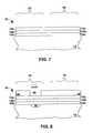
- FIGS. 7-12Another aspect of the present invention is described in FIGS. 7-12.
- a semiconductor structure 10is shown with a semiconductor substrate 12 under a charge trapping dielectric 14 .
- Semiconductor structure 10contains two regions, the core region 16 containing the memory cells and the periphery region 18 containing the rest of the chip such as the controlling logic and input/output devices.
- the charge trapping dielectric 14contains three layers; namely, a first silicon dioxide layer 14 a, a silicon nitride layer 14 b, and a second silicon dioxide layer 14 c (an ONO dielectric).
- the electron trappingis in the silicon nitride layer 14 b.
- the charge trapping dielectric 14may be any dielectric layer or layers that are capable of or facilitate electron trapping.
- charge trapping dielectricsinclude an ONO trilayer dielectric, an oxide/nitride bilayer dielectric, a nitride/oxide bilayer dielectric, an oxide/tantalum oxide bilayer dielectric, an oxide/tantalum oxide/oxide trilayer dielectric, an oxide/strontium titanate bilayer dielectric, an oxide/barium strontium titanate bilayer dielectric, an oxide/strontium titanate/oxide trilayer dielectric, an oxide/strontium titanate/barium strontium titanate trilayer dielectric, an oxide/hafnium oxide/oxide trilayer dielectric, and the like.
- one or both of the silicon dioxide layers 14 a and 14 cmay be a silicon-rich silicon dioxide layer.
- One or both of the silicon dioxide layers 14 a and 14 cmay also be an oxygen-rich silicon dioxide layer.
- One or both of the silicon dioxide layers 14 a and 14 cmay be a thermally grown or a deposited oxide.
- One or both of the silicon dioxide layers 14 a and 14 cmay be nitrided oxide layers.
- the nitride 14 bmay be a silicon-rich silicon nitride layer.
- the nitride 14 bmay also be an nitrogen-rich silicon nitride layer.
- a threshold implant (V T adjustment implant) stepmay be conducted before formation of the charge trapping dielectric 14 over the structure.
- a blanket implantation of boronmay be performed just prior to forming the charge trapping dielectric 14 .
- this implantation stepmay be conducted before or after the bitline implantation step.
- a masksuch as a suitable photoresist 36 is used to partially cover the charge trapping dielectric 14 in the core region 16 while covering the charge trapping dielectric 14 in the periphery region 18 of the structure 10 .
- photoresist 36is patterned such that there are openings 25 therein.
- the photoresist 36is patterned in the core region 16 to facilitate/correspond to the formation of the buried bitlines (that is, areas of the charge trapping dielectric 14 directly over the subsequently formed buried bitlines are exposed by the patterned photoresist 36 ). Ions are implanted, as shown by the arrows, forming implanted region 26 directly below opening 25 .
- the semiconductor structure 10is optionally annealed at a suitable temperature after implantation.
- One or more suitable implantation materialsmay be employed.
- the selection of implantation materialsprimarily depends on the type of substrate employed, for example, whether a p-type or n-type is used (p+, p ⁇ , n+, or n ⁇ ).
- Examples of implantation materialsinclude one or more of arsenic, boron, and phosphorus.
- the implantation materialsare implanted at a dosage suitable to form buried bitlines.
- the implantation materialsare implanted at a dosage from about 1 ⁇ 10 14 to about 1 ⁇ 10 16 atoms/cm 2 .
- the implantation materialsare implanted at a dosage from about 5 ⁇ 10 14 to about 7 ⁇ 10 15 atoms/cm 2 .
- the implantation materialsare implanted at a dosage from about 1 ⁇ 10 15 to about 5 ⁇ 10 15 atoms/cm 2 .
- Implanted regions 26which correspond to the openings 25 , form the buried bitlines in the resultant SONOS type nonvolatile memory device.
- the width of the implanted regions 26at least substantially correspond to the width of the openings 25 .
- a V T adjustment implant stepmay optionally be conducted before or after the bitline implantation step.
- the structure 10may be tilted relative to the angle of implantation and implantation of boron may occur through openings 25 in the photoresist 36 in the core region 16 to form implanted regions (not shown) adjacent implanted regions 26 .
- the V T adjustment implant steptypically employs a type dopant opposite that of the bitline implantation species.
- photoresist 36is stripped or removed from the structure 10 and another mask such as a suitable photoresist 38 is used to cover the charge trapping dielectric 14 in the core region 16 leaving the charge trapping dielectric 14 exposed in the periphery region 18 of the structure 10 .
- the charge trapping dielectric 14 exposed in the periphery region 18is etched down to the substrate 12 (the first silicon dioxide layer 14 a, the silicon nitride layer 14 b, and the second silicon dioxide layer 14 c are removed in the periphery region 18 of the structure 10 ). Multiple etching steps may be employed to remove the charge trapping dielectric 14 .
- a gate dielectric 22such as an oxide layer is provided using any suitable means, such as CVD, dry oxidation, wet oxidation or rapid thermal oxidation, on at least a portion of the exposed portions of the substrate 12 (over the periphery region 18 ). Dry oxidation, wet oxidation, and rapid thermal oxidation are preferred, especially when gate dielectric 22 contains silicon dioxide. CVD techniques are employed in instances where the gate dielectric 22 contains one or more of silicon dioxide, silicon nitride, and silicon oxynitride.
- the gate dielectric 22later serves as the gate dielectric for subsequently formed high and/or low voltage transistors (not shown) in the periphery region 18 .
- the gate dielectric 22has a thickness from about 30 ⁇ to about 300 ⁇ . In another embodiment, the gate dielectric 22 has a thickness from about 40 ⁇ to about 250 ⁇ .
- photoresist 38is stripped or removed from the semiconductor structure 10 .
- patterned photoresist 38is removed from the structure 10 , and polysilicon gates 28 are formed over the structure 10 .
- polysiliconor doped amorphous silicon
- the polysilicon layeris then patterned using suitable techniques to form polysilicon gates 28 .
- a photoresist(not shown) may be deposited and patterned using standard lithographic techniques covering a portion and exposing a portion of the polysilicon layer. The exposed portions of the polysilicon layer are removed by standard techniques, such as using anisotropic etching.
- a SONOS type memory cell 30 formed in the core region of a SONOS type memory deviceis shown.
- the cellcontains charge trapping dielectric 14 , gate 28 , source 32 , and drain 34 .
- SONOS type memory cell 30can function and operate as a single bit cell or a double bit cell.
- FIGS. 13-19One aspect of the present invention is described in FIGS. 13-19.
- a semiconductor structure 10is shown with a semiconductor substrate 12 under a charge trapping dielectric 14 .
- Semiconductor structure 10contains two regions, the core region 16 containing the memory cells and the periphery region 18 containing the rest of the chip such as the controlling logic and input/output devices.
- the charge trapping dielectric 14contains three layers; namely, a first silicon dioxide layer 14 a, a silicon nitride layer 14 b, and a second silicon dioxide layer 14 c (an ONO dielectric). Particularly in the case of an ONO dielectric, the electron trapping is in the silicon nitride layer 14 b.
- the charge trapping dielectric 14may be any dielectric layer or layers that are capable of or facilitate electron trapping.
- charge trapping dielectricsinclude an ONO trilayer dielectric, an oxide/nitride bilayer dielectric, a nitride/oxide bilayer dielectric, an oxide/tantalum oxide bilayer dielectric, an oxide/tantalum oxide/oxide trilayer dielectric, an oxide/strontium titanate bilayer dielectric, an oxide/barium strontium titanate bilayer dielectric, an oxide/strontium titanate/oxide trilayer dielectric, an oxide/strontium titanate/barium strontium titanate trilayer dielectric, an oxide/hafnium oxide/oxide trilayer dielectric, and the like.
- one or both of the silicon dioxide layers 14 a and 14 cmay be a silicon-rich silicon dioxide layer.
- One or both of the silicon dioxide layers 14 a and 14 cmay also be an oxygen-rich silicon dioxide layer.
- One or both of the silicon dioxide layers 14 a and 14 cmay be a thermally grown or a deposited oxide.
- One or both of the silicon dioxide layers 14 a and 14 cmay be nitrided oxide layers.
- the nitride 14 bmay be a silicon-rich silicon nitride layer.
- the nitride 14 bmay also be an nitrogen-rich silicon nitride layer.
- a threshold implant (V T adjustment implant) stepmay be conducted before formation of the charge trapping dielectric 14 over the structure.
- a blanket implantation of boronmay be performed just prior to forming the charge trapping dielectric 14 .
- this implantation stepmay be conducted before or after the bitline implantation step.
- a mask such as a suitable photoresist 20is used to cover the charge trapping dielectric 14 in the core region 16 leaving the charge trapping dielectric 14 exposed in the periphery region 18 of the structure 10 .
- the charge trapping dielectric 14 exposed in the periphery region 18is etched down to the substrate 12 (the first silicon dioxide layer 14 a, the silicon nitride layer 14 b, and the second silicon dioxide layer 14 c are removed in the periphery region 18 of the structure 10 ). Multiple etching steps may be employed to remove the charge trapping dielectric 14 .
- a gate dielectric 22such as an oxide layer is provided using any suitable means, such as dry oxidation, wet oxidation, rapid thermal oxidation, or CVD, on at least a portion of the exposed portions of the substrate 12 (over the periphery region 18 ). Dry oxidation, wet oxidation, and rapid thermal oxidation are preferred, especially when gate dielectric 22 contains silicon dioxide. CVD techniques may be employed in instances where the gate dielectric 22 contains one or more of silicon dioxide, silicon nitride, and silicon oxynitride.
- the gate dielectric 22later serves as the gate dielectric for subsequently formed high and/or low voltage transistors (not shown) in the periphery region 18 .
- the gate dielectric 22has a thickness from about 30 ⁇ to about 300 ⁇ . In another embodiment, the gate dielectric 22 has a thickness from about 40 ⁇ to about 250 ⁇ .
- photoresist 20is stripped or removed from the semiconductor structure 10 .
- another masksuch as a suitable photoresist 24 is used to partially cover the charge trapping dielectric 14 in the core region 16 while covering the gate dielectric 22 in the periphery region 18 of the structure 10 .
- photoresist 24is patterned such that there are openings 25 therein.
- the photoresist 24is patterned in the core region 16 to facilitate/correspond to the formation of the buried bitlines (that is, areas of the charge trapping dielectric 14 directly over the subsequently formed buried bitlines are exposed by the patterned photoresist 24 ). Ions are implanted, as shown by the arrows, forming implanted region 26 in the substrate 12 directly below opening 25 .
- the semiconductor structure 10is optionally annealed at a suitable temperature after implantation.
- One or more suitable implantation materialsmay be employed.
- the selection of implantation materialsprimarily depends on the type of substrate employed, for example, whether a p-type or n-type is used (p+, p ⁇ , n+, or n ⁇ ).
- Examples of implantation materialsinclude one or more of arsenic, boron, and phosphorus.
- the implantation materialsare implanted at a dosage suitable to form buried bitlines.
- the implantation materialsare implanted at a dosage from about 1 ⁇ 10 14 to about 1 ⁇ 10 16 atoms/cm 2 .
- the implantation materialsare implanted at a dosage from about 5 ⁇ 10 14 to about 7 ⁇ 10 15 atoms/cm 2 .
- the implantation materialsare implanted at a dosage from about 1 ⁇ 10 15 to about 5 ⁇ 10 15 atoms/cm 2 .
- Implanted regions 26which correspond to the openings 25 , form the buried bitlines in the resultant SONOS type nonvolatile memory device.
- the width of the implanted regions 26at least substantially correspond to the width of the openings 25 .
- a V T adjustment implant stepmay optionally be conducted before or after the bitline implantation step.
- the structure 10may be tilted relative to the angle of implantation and implantation of boron may occur through openings 25 in the photoresist 24 in the core region 16 to form implanted regions (not shown) adjacent implanted regions 26 .
- the V T adjustment implant steptypically employs a type dopant opposite that of the bitline implantation species.
- patterned photoresist 24is removed from the structure 10 , and additional gate dielectric material is formed in the periphery region 18 thereby providing a size enhanced (increased thickness) and/or cleaner gate dielectric 40 .
- the additional gate dielectric materialis preferably formed by thermal growth versus deposition, using any suitable means, such as dry oxidation, wet oxidation or rapid thermal oxidation, although CVD techniques may be employed. Dry oxidation, wet oxidation, and rapid thermal oxidation are preferred, especially when gate dielectric 40 contains silicon dioxide. In instances where the entire structure is subject to the oxidation treatment, the presence of the silicon nitride layer 14 b substantially impedes the growth of oxide in the silicon dioxide layer 14 c of the core region 16 .
- CVD techniquesare employed in instances where the gate dielectric 40 contains one or more of silicon dioxide, silicon nitride, and silicon oxynitride. In instances where CVD techniques are employed, it is preferable to mask the core region (not shown).
- the growth or regrowth of additional periphery gate dielectric materialserves to provide a cleaner gate dielectric over which to subsequently form gates and/or increase the thickness of the gate dielectrics in the periphery region 18 .
- Forming the gate dielectric 40 in two stepscontributes to a reduction in unwanted diffusion of the bitline implants.
- the size enhanced gate dielectric 40has a thickness from about 30 ⁇ to about 350 ⁇ .
- the size enhanced gate dielectric 40has a thickness from about 40 ⁇ to about 300 ⁇ .
- the size enhanced gate dielectric 40has a thickness that is at least about 10% larger than the thickness of gate dielectric 22 .
- a portion of the gate dielectric 22 in the periphery region 18may be removed (using, for example, lithographic techniques) leaving the periphery region 18 partially covered by the gate dielectric 22 when the growth or regrowth of additional periphery gate dielectric material is conducted.
- the remaining portion of the gate dielectric 22is formed into the size enhanced gate dielectric, while fresh gate dielectric is formed in the portions where the gate dielectric 22 is previously removed.
- Thisis advantageous when different subsequently formed gates in the periphery region 18 require gate dielectrics of different thickness. For instance, high voltage gate transistors may require thicker gate oxides than low voltage gate transistors.
- the size enhanced gate dielectric 40may have two or more thicknesses. The growth or regrowth of additional periphery gate dielectric material is therefore conducted in one or more steps, two or more steps, etc.
- polysilicon gates 28are formed over the structure 10 .
- polysiliconor doped amorphous silicon
- the polysilicon layeris then patterned using suitable techniques to form polysilicon gates 28 .
- a photoresistmay be deposited and patterned using standard lithographic techniques covering a portion and exposing a portion of the polysilicon layer. The exposed portions of the polysilicon layer are removed by standard techniques, such as using anisotropic etching.
- a SONOS type memory cell 30 formed in the core region of a SONOS type memory deviceis shown.
- the cellcontains charge trapping dielectric 14 , gate 29 , source 32 , and drain 34 .
- SONOS type memory cell 30can function and operate as a single bit cell or a double bit cell.
- the structureis substantially planar and contains a substrate 12 , charge trapping dielectric 14 , polysilicon gates/wordlines 28 , and buried bitlines 26 .
- the polysilicon gates/wordlines 28have a planar or substantially planar orientation while having a substantially uniform thickness.
- the charge trapping dielectric 14contains three layers 14 a, 14 b, and 14 c, such as an ONO dielectric, an oxide/tantalum oxide/oxide dielectric, an oxide/strontium titanate/oxide dielectric, an oxide/strontium titanate/barium strontium titanate dielectric, or an oxide/hafnium oxide/oxide dielectric.
- the dashed linesshow the extension of the buried bitlines 26 through substrate 12 .
- FIG. 21a perspective illustration of the core region of another SONOS type memory device is shown.
- the structureis substantially planar and contains a substrate 12 , charge trapping dielectric 14 , polysilicon gates/wordlines 28 , and buried bitlines 26 .
- the polysilicon gates/wordlines 28have a planar or substantially planar orientation while having a substantially uniform thickness.
- the charge trapping dielectric 14contains two layers 14 a and 14 b, such as an oxide/nitride dielectric, a nitride/oxide dielectric, an oxide/tantalum oxide dielectric, an oxide/strontium titanate dielectric, or an oxide/barium strontium titanate dielectric.
- the dashed linesshow the extension of the buried bitlines 26 through substrate 12 .
- FIG. 22a portion of the core region of a prior art SONOS type memory devices according to Mitchell et al U.S. Pat. No. 5,168,334 is shown.
- FIG. 22is analogous to FIG. 5 of Mitchell et al U.S. Pat. No. 5,168,334.
- FIG. 22shows silicon substrate 42 having field oxide regions 43 , bitlines 44 and 46 , ONO trilayer 50/52/54, and polysilicon wordline 56 .
- the structure of prior art FIG. 22is non-planar, due to the presence of oxide regions 43 . Consequently, the polysilicon wordline 56 is non-planar.
- oxide isolationsuch as LOCOS
- planar orientation of the core regionscontributes to a number of advantages for the non-volatile semiconductor memory devices of the present invention.
- planar non-volatile semiconductor memory devicesdo not require an etch step for making the bitlines, thus, the process of fabricating such devices is simplified.
- the fabrication of planar non-volatile semiconductor memory devicesprovides a controllable junction (improved diffusion control). That is, boron segregation is minimized and/or eliminated and the final arsenic dopant profile is not effected by oxidation enhanced diffusion.
- the less severe topographyenables improved linewidth control (and generally improved lithographic manipulations) compared to memory devices having non-planar orientations.
- topographyminimizes and/or eliminates stringer formation.
- the less severe topographyalso results in better yields compared to memory devices having non-planar orientations.
- handling and packaging planar non-volatile semiconductor memory devicesis easier and more efficient than non-planar memory devices.
- the channel lengthsbecome shorter and short channel effects take hold.
- short channel effectsmay become prevalent sooner than in the case of the single bit transistor.
- short channeling effectsare minimized, since there is no LOCOS in the core region.
- Reading in the same direction as programmingmeans the device is programmed and read in the same forward direction.
- voltages having levels lower than that during programmingare applied to the gate and drain and the channel current is sensed.
- a dramatic reduction in programing timeis achieved due to amplification of the effect of the trapped charge injected into the nitride layer brought about by reading the memory cell device in the opposite direction from which it was programmed.
- Reading in the backward directionmeans reading in a direction opposite than that of programming. In other words, voltage is applied to the source 32 and the gate 28 and the drain 34 is grounded or at a lower voltage.
- each biti.e., the left and right bit
- each bitis treated as if the cell 30 is a single bit cell.
- both the left and right bitsare programmed as previously described.
- programming voltagesare applied to the gate 28 and drain 34 and hot electrons are injected into and trapped in the charge trapping layer 14 b in the region near the drain 34 .
- the left bitis programmed by applying programming voltages to the gate 28 and source 32 , which now functions as the drain for the left bit.
- the threshold voltage for a programmed left bitis relatively low compared to the threshold voltage for the right bit and thus the state of the right bit can be read without interference from the left bit.
- the unprogrammed left bitremains unprogrammed.
- the gate voltage during programmingis sufficiently high that the programmed right bit does not substantially interfere with the programming of the left bit.
- the left bitremains unprogrammed during the programming of the right bit.
- the left bitis programmed and the right bit remains programmed and can still be read.
- the right bitcan be programmed through during programming of the left bit. Further, the programming of the left bit does not disturb the programmed right bit.
- each bitis treated as if the cell 30 is a single bit cell.
- the right bitis read in the reverse direction by applying read voltages to the source 32 and the gate 28 and grounding or applying a lower voltage to the drain 34 .
- read voltagesare applied to the gate 28 and to the drain 34 and the source 32 is grounded or at a lower voltage.
- a read of the two bit memory device of the present inventionfalls into one of three cases: (1) neither of the two bits are programmed (2) one of the bits is programmed and the other is not or (3) both of the bits are programmed.
- eraseinvolves tunneling enhanced hot hole injection through the bottom oxide 14 a. Hole flow is generated by band to band tunneling in a deep depletion layer under the charge trapping layer 14 above a junction. Holes increase their energy due to the lateral field and they are injected through the bottom oxide 14 a of the charge trapping layer 14 , where they recombine with the electrons or are trapped.
- eraseis typically performed by simultaneously applying a positive potential to the source 32 or the drain 34 and zero potential, i.e., ground, or lower voltage potential to the gate 28 . Alternatively, erase is performed by simultaneously applying a positive potential to the source 32 or the drain 34 and negative potential to the gate 28 .
- an eraseis performed by removing electrons from the charge trapping nitride region either through the gate 28 via the top oxide 14 c or through the drain 34 via the bottom oxide 14 a.
- an eraseis performed by removing electrons from the charge trapping nitride region either through the gate 28 via the top oxide 14 c or through the source 32 via the bottom oxide 14 a. Erasing of one of the bits does not affect the other bit because the erase voltage is localized to the junction adjacent to the bit that is to be erased.
- one technique of erasingis to simultaneously apply a negative potential to the gate 28 and a positive potential to the drain 34 such that electron tunneling occurs from the charge trapping nitride layer 14 b to the drain 34 via the bottom oxide 14 a.
- the left bitis erased in a similar fashion except that a positive potential is applied to the source 32 rather than the drain 34 .
- a second techniqueis to simultaneously apply a positive voltage potential to the gate 28 and zero potential, i.e., ground, or lower voltage potential to the drain 34 such that electron tunneling occurs from the charge trapping nitride layer 14 b through the top oxide 14 c to the gate 28 .
- the right bitis erased in a similar fashion with zero potential or lower voltage potential applied to the source 32 .
Landscapes
- Non-Volatile Memory (AREA)
- Semiconductor Memories (AREA)
Abstract
Description
Claims (17)
Priority Applications (6)
| Application Number | Priority Date | Filing Date | Title |
|---|---|---|---|
| US09/893,026US6541816B2 (en) | 2000-11-28 | 2001-06-27 | Planar structure for non-volatile memory devices |
| EP01999006AEP1338037B1 (en) | 2000-11-28 | 2001-11-15 | Non-volatile SONOS semiconductor memory device |
| PCT/US2001/046124WO2002045171A1 (en) | 2000-11-28 | 2001-11-15 | Planar structure and methods of fabricating non-volatile memory devices |
| AU2002220164AAU2002220164A1 (en) | 2000-11-28 | 2001-11-15 | Planar structure and methods of fabricating non-volatile memory devices |
| DE60144340TDE60144340D1 (en) | 2000-11-28 | 2001-11-15 | Non-volatile SONOS semiconductor memory device |
| TW090129264ATW518726B (en) | 2000-11-28 | 2001-11-27 | Planar structure and methods of fabricating non-volatile memory device |
Applications Claiming Priority (2)
| Application Number | Priority Date | Filing Date | Title |
|---|---|---|---|
| US09/723,635US6465306B1 (en) | 2000-11-28 | 2000-11-28 | Simultaneous formation of charge storage and bitline to wordline isolation |
| US09/893,026US6541816B2 (en) | 2000-11-28 | 2001-06-27 | Planar structure for non-volatile memory devices |
Related Parent Applications (1)
| Application Number | Title | Priority Date | Filing Date |
|---|---|---|---|
| US09/723,635Continuation-In-PartUS6465306B1 (en) | 2000-11-28 | 2000-11-28 | Simultaneous formation of charge storage and bitline to wordline isolation |
Publications (2)
| Publication Number | Publication Date |
|---|---|
| US20020063277A1 US20020063277A1 (en) | 2002-05-30 |
| US6541816B2true US6541816B2 (en) | 2003-04-01 |
Family
ID=24907066
Family Applications (3)
| Application Number | Title | Priority Date | Filing Date |
|---|---|---|---|
| US09/723,635Expired - LifetimeUS6465306B1 (en) | 2000-11-28 | 2000-11-28 | Simultaneous formation of charge storage and bitline to wordline isolation |
| US09/893,026Expired - Fee RelatedUS6541816B2 (en) | 2000-11-28 | 2001-06-27 | Planar structure for non-volatile memory devices |
| US10/223,195Expired - Fee RelatedUS6555436B2 (en) | 2000-11-28 | 2002-08-19 | Simultaneous formation of charge storage and bitline to wordline isolation |
Family Applications Before (1)
| Application Number | Title | Priority Date | Filing Date |
|---|---|---|---|
| US09/723,635Expired - LifetimeUS6465306B1 (en) | 2000-11-28 | 2000-11-28 | Simultaneous formation of charge storage and bitline to wordline isolation |
Family Applications After (1)
| Application Number | Title | Priority Date | Filing Date |
|---|---|---|---|
| US10/223,195Expired - Fee RelatedUS6555436B2 (en) | 2000-11-28 | 2002-08-19 | Simultaneous formation of charge storage and bitline to wordline isolation |
Country Status (8)
| Country | Link |
|---|---|
| US (3) | US6465306B1 (en) |
| EP (1) | EP1338034B1 (en) |
| JP (1) | JP5132024B2 (en) |
| KR (1) | KR100810710B1 (en) |
| CN (1) | CN100530600C (en) |
| AU (1) | AU2001283186A1 (en) |
| DE (2) | DE60141035D1 (en) |
| WO (1) | WO2002045157A1 (en) |
Cited By (64)
| Publication number | Priority date | Publication date | Assignee | Title |
|---|---|---|---|---|
| US20030039153A1 (en)* | 2001-01-18 | 2003-02-27 | Eduardo Maayan | EEPROM array and method for operation thereof |
| US20030038312A1 (en)* | 2001-08-20 | 2003-02-27 | Thomas Mikolajick | Memory element for a semiconductor memory device |
| US20030234420A1 (en)* | 2002-06-21 | 2003-12-25 | Micron Technology, Inc. | Write once read only memory with large work function floating gates |
| US20040004247A1 (en)* | 2002-07-08 | 2004-01-08 | Micron Technology, Inc. | Memory utilizing oxide-nitride nanolaminates |
| US20040004859A1 (en)* | 2002-07-08 | 2004-01-08 | Micron Technology, Inc. | Memory utilizing oxide nanolaminates |
| US20040008541A1 (en)* | 2002-07-10 | 2004-01-15 | Eduardo Maayan | Multiple use memory chip |
| US20040121544A1 (en)* | 2002-12-24 | 2004-06-24 | Kent Kuohua Chang | High-k tunneling dielectric for read only memory device and fabrication method thereof |
| US20040130951A1 (en)* | 2002-06-21 | 2004-07-08 | Micron Technology, Inc. | Write once read only memory employing charge trapping in insulators |
| US6787458B1 (en) | 2003-07-07 | 2004-09-07 | Advanced Micro Devices, Inc. | Polymer memory device formed in via opening |
| US6803267B1 (en) | 2003-07-07 | 2004-10-12 | Advanced Micro Devices, Inc. | Silicon containing material for patterning polymeric memory element |
| US20040212004A1 (en)* | 2003-04-25 | 2004-10-28 | Bohumil Lojek | Mirror image non-volatile memory cell transistor pairs with single poly layer |
| US20040215422A1 (en)* | 2001-05-24 | 2004-10-28 | Robert Dodge | System and method for facilitating welding system diagnostics |
| US6818944B2 (en)* | 2002-04-12 | 2004-11-16 | Samsung Electronics Co., Ltd. | Nonvolatile memory devices and methods of fabricating the same |
| US20040238864A1 (en)* | 2003-06-02 | 2004-12-02 | Tripsas Nicholas H. | Planar polymer memory device |
| US20050056882A1 (en)* | 2003-04-25 | 2005-03-17 | Bohumil Lojek | Mirror image memory cell transistor pairs featuring poly floating spacers |
| US20050111257A1 (en)* | 1997-08-01 | 2005-05-26 | Boaz Eitan | Two bit non-volatile electrically erasable and programmable semiconductor memory cell utilizing asymmetrical charge trapping |
| US20050142801A1 (en)* | 2003-12-30 | 2005-06-30 | Dongbuanam Semiconductor Inc. | Method for manufacturing semiconductor device |
| US20050224922A1 (en)* | 2004-04-02 | 2005-10-13 | Lyons Christopher F | Polymer dielectrics for memory element array interconnect |
| US20050260798A1 (en)* | 2002-12-09 | 2005-11-24 | Progressant Technologies, Inc. | Method of forming a negative differential resistance device |
| US6969689B1 (en)* | 2002-06-28 | 2005-11-29 | Krishnaswamy Ramkumar | Method of manufacturing an oxide-nitride-oxide (ONO) dielectric for SONOS-type devices |
| US20050281121A1 (en)* | 1996-10-29 | 2005-12-22 | Micron Technology, Inc. | Memory system, method and predecoding circuit operable in different modes for selectively accessing multiple blocks of memory cells for simultaneous writing or erasure |
| US20060001080A1 (en)* | 2002-06-21 | 2006-01-05 | Micron Technology, Inc. | Write once read only memory employing floating gates |
| US20060008966A1 (en)* | 2002-07-08 | 2006-01-12 | Micron Technology, Inc. | Memory utilizing oxide-conductor nanolaminates |
| US20060036803A1 (en)* | 2004-08-16 | 2006-02-16 | Mori Edan | Non-volatile memory device controlled by a micro-controller |
| US20060076598A1 (en)* | 2004-09-29 | 2006-04-13 | Masahiko Higashi | Semiconductor device and method of fabrication |
| US20060081915A1 (en)* | 2004-10-19 | 2006-04-20 | Fujitsu Limited | Nonvolatile semiconductor memory device and method for fabricating the same |
| US20060113583A1 (en)* | 2003-04-25 | 2006-06-01 | Atmel Corporation | Twin EEPROM memory transistors with subsurface stepped floating gates |
| US20070087503A1 (en)* | 2005-10-17 | 2007-04-19 | Saifun Semiconductors, Ltd. | Improving NROM device characteristics using adjusted gate work function |
| US7221138B2 (en) | 2005-09-27 | 2007-05-22 | Saifun Semiconductors Ltd | Method and apparatus for measuring charge pump output current |
| US7232724B1 (en) | 2005-04-25 | 2007-06-19 | Advanced Micro Devices, Inc. | Radical oxidation for bitline oxide of SONOS |
| US20070281423A1 (en)* | 2006-06-02 | 2007-12-06 | Yen-Hao Shih | Method for manufacuring semiconductor device |
| US20070291551A1 (en)* | 2006-06-14 | 2007-12-20 | Macronix International Co., Ltd. | Nonvolatitle memory array and method for operating thereof |
| US20070297227A1 (en)* | 2006-06-21 | 2007-12-27 | Macronix International Co., Ltd. | Multi-Level Cell Memory Structures with Enlarged Second Bit Operation Window |
| US20070297240A1 (en)* | 2006-06-21 | 2007-12-27 | Macronix International Co., Ltd. | Methods and Structures for Expanding a Memory Operation Window and Reducing a Second Bit Effect |
| US7317633B2 (en) | 2004-07-06 | 2008-01-08 | Saifun Semiconductors Ltd | Protection of NROM devices from charge damage |
| US20080064158A1 (en)* | 2006-09-12 | 2008-03-13 | Macronix International Co., Ltd. | Method for fabricating non-volatile memory |
| US7348237B2 (en) | 2002-06-21 | 2008-03-25 | Micron Technology, Inc. | NOR flash memory cell with high storage density |
| US7352627B2 (en) | 2006-01-03 | 2008-04-01 | Saifon Semiconductors Ltd. | Method, system, and circuit for operating a non-volatile memory array |
| US7369440B2 (en) | 2005-01-19 | 2008-05-06 | Saifun Semiconductors Ltd. | Method, circuit and systems for erasing one or more non-volatile memory cells |
| US7420848B2 (en) | 2002-01-31 | 2008-09-02 | Saifun Semiconductors Ltd. | Method, system, and circuit for operating a non-volatile memory array |
| US7457183B2 (en) | 2003-09-16 | 2008-11-25 | Saifun Semiconductors Ltd. | Operating array cells with matched reference cells |
| US7466594B2 (en) | 2004-08-12 | 2008-12-16 | Saifun Semiconductors Ltd. | Dynamic matching of signal path and reference path for sensing |
| US7512009B2 (en) | 2001-04-05 | 2009-03-31 | Saifun Semiconductors Ltd. | Method for programming a reference cell |
| US7532529B2 (en) | 2004-03-29 | 2009-05-12 | Saifun Semiconductors Ltd. | Apparatus and methods for multi-level sensing in a memory array |
| US7535765B2 (en) | 2004-12-09 | 2009-05-19 | Saifun Semiconductors Ltd. | Non-volatile memory device and method for reading cells |
| US7605579B2 (en) | 2006-09-18 | 2009-10-20 | Saifun Semiconductors Ltd. | Measuring and controlling current consumption and output current of charge pumps |
| US7638850B2 (en) | 2004-10-14 | 2009-12-29 | Saifun Semiconductors Ltd. | Non-volatile memory structure and method of fabrication |
| US7638835B2 (en) | 2006-02-28 | 2009-12-29 | Saifun Semiconductors Ltd. | Double density NROM with nitride strips (DDNS) |
| US7668017B2 (en) | 2005-08-17 | 2010-02-23 | Saifun Semiconductors Ltd. | Method of erasing non-volatile memory cells |
| US7675782B2 (en) | 2002-10-29 | 2010-03-09 | Saifun Semiconductors Ltd. | Method, system and circuit for programming a non-volatile memory array |
| US7692961B2 (en) | 2006-02-21 | 2010-04-06 | Saifun Semiconductors Ltd. | Method, circuit and device for disturb-control of programming nonvolatile memory cells by hot-hole injection (HHI) and by channel hot-electron (CHE) injection |
| US7701779B2 (en) | 2006-04-27 | 2010-04-20 | Sajfun Semiconductors Ltd. | Method for programming a reference cell |
| US7709402B2 (en) | 2006-02-16 | 2010-05-04 | Micron Technology, Inc. | Conductive layers for hafnium silicon oxynitride films |
| US7743230B2 (en) | 2003-01-31 | 2010-06-22 | Saifun Semiconductors Ltd. | Memory array programming circuit and a method for using the circuit |
| US7760554B2 (en) | 2006-02-21 | 2010-07-20 | Saifun Semiconductors Ltd. | NROM non-volatile memory and mode of operation |
| US7786512B2 (en) | 2005-07-18 | 2010-08-31 | Saifun Semiconductors Ltd. | Dense non-volatile memory array and method of fabrication |
| US7808818B2 (en) | 2006-01-12 | 2010-10-05 | Saifun Semiconductors Ltd. | Secondary injection for NROM |
| CN101097951B (en)* | 2006-06-27 | 2011-03-02 | 旺宏电子股份有限公司 | Non-volatile memory cell structure and operation method |
| US8053812B2 (en) | 2005-03-17 | 2011-11-08 | Spansion Israel Ltd | Contact in planar NROM technology |
| US8253452B2 (en) | 2006-02-21 | 2012-08-28 | Spansion Israel Ltd | Circuit and method for powering up an integrated circuit and an integrated circuit utilizing same |
| US20170018430A1 (en)* | 2015-07-16 | 2017-01-19 | Silergy Semiconductor Technology (Hangzhou) Ltd | Semiconductor structure and manufacture method thereof |
| US9893172B2 (en)* | 2014-01-21 | 2018-02-13 | Cypress Semiconductor Corporation | Methods to integrate SONOS into CMOS flow |
| US10446401B2 (en)* | 2017-11-29 | 2019-10-15 | Renesas Electronics Corporation | Method of manufacturing semiconductor device |
| US11311958B1 (en)* | 2019-05-13 | 2022-04-26 | Airgas, Inc. | Digital welding and cutting efficiency analysis, process evaluation and response feedback system for process optimization |
Families Citing this family (62)
| Publication number | Priority date | Publication date | Assignee | Title |
|---|---|---|---|---|
| US7234274B2 (en)* | 2001-07-10 | 2007-06-26 | Kabushikikaisha Ansei | Vehicle door |
| TW519734B (en)* | 2001-12-04 | 2003-02-01 | Macronix Int Co Ltd | Programming and erasing methods of non-volatile memory having nitride tunneling layer |
| JP2003243544A (en)* | 2002-02-20 | 2003-08-29 | Mitsubishi Electric Corp | Nonvolatile semiconductor memory device and method of manufacturing the same |
| US6617215B1 (en)* | 2002-03-27 | 2003-09-09 | Advanced Micro Devices, Inc. | Memory wordline hard mask |
| US7927950B2 (en)* | 2002-05-07 | 2011-04-19 | Samsung Electronics Co., Ltd. | Method of fabricating trap type nonvolatile memory device |
| KR100655441B1 (en)* | 2005-09-01 | 2006-12-08 | 삼성전자주식회사 | Manufacturing method of trap type nonvolatile memory device |
| KR100437451B1 (en)* | 2002-05-07 | 2004-06-23 | 삼성전자주식회사 | Method Of Fabricating Trap-type Nonvolatile Memory Device |
| US6567292B1 (en) | 2002-06-28 | 2003-05-20 | Progressant Technologies, Inc. | Negative differential resistance (NDR) element and memory with reduced soft error rate |
| US7095659B2 (en)* | 2002-06-28 | 2006-08-22 | Progressant Technologies, Inc. | Variable voltage supply bias and methods for negative differential resistance (NDR) based memory device |
| US6864104B2 (en)* | 2002-06-28 | 2005-03-08 | Progressant Technologies, Inc. | Silicon on insulator (SOI) negative differential resistance (NDR) based memory device with reduced body effects |
| US6912151B2 (en)* | 2002-06-28 | 2005-06-28 | Synopsys, Inc. | Negative differential resistance (NDR) based memory device with reduced body effects |
| US6853035B1 (en)* | 2002-06-28 | 2005-02-08 | Synopsys, Inc. | Negative differential resistance (NDR) memory device with reduced soft error rate |
| US6795337B2 (en)* | 2002-06-28 | 2004-09-21 | Progressant Technologies, Inc. | Negative differential resistance (NDR) elements and memory device using the same |
| US7098472B2 (en)* | 2002-06-28 | 2006-08-29 | Progressant Technologies, Inc. | Negative differential resistance (NDR) elements and memory device using the same |
| US6847562B2 (en)* | 2002-06-28 | 2005-01-25 | Progressant Technologies, Inc. | Enhanced read and write methods for negative differential resistance (NDR) based memory device |
| KR100446632B1 (en)* | 2002-10-14 | 2004-09-04 | 삼성전자주식회사 | Nonvolatile Silicon/Oxide/Nitride/Silicon/ Nitride/Oxide/ Silicon memory |
| US7394703B2 (en)* | 2002-10-15 | 2008-07-01 | Halo Lsi, Inc. | Twin insulator charge storage device operation and its fabrication method |
| US6730957B1 (en)* | 2002-11-05 | 2004-05-04 | Winbond Electronics Corporation | Non-volatile memory compatible with logic devices and fabrication method thereof |
| US6979580B2 (en)* | 2002-12-09 | 2005-12-27 | Progressant Technologies, Inc. | Process for controlling performance characteristics of a negative differential resistance (NDR) device |
| US7012833B2 (en)* | 2002-12-09 | 2006-03-14 | Progressant Technologies, Inc. | Integrated circuit having negative differential resistance (NDR) devices with varied peak-to-valley ratios (PVRs) |
| US6812084B2 (en)* | 2002-12-09 | 2004-11-02 | Progressant Technologies, Inc. | Adaptive negative differential resistance device |
| US6806117B2 (en)* | 2002-12-09 | 2004-10-19 | Progressant Technologies, Inc. | Methods of testing/stressing a charge trapping device |
| US6849483B2 (en)* | 2002-12-09 | 2005-02-01 | Progressant Technologies, Inc. | Charge trapping device and method of forming the same |
| DE10259783A1 (en)* | 2002-12-19 | 2004-07-15 | Infineon Technologies Ag | Method for improving process step sequence in forming semiconductor memories with charge trapping memory cells, used same masks as used for forming doped troughs outside memory cell field for removing HV gate dielectric |
| US7005711B2 (en)* | 2002-12-20 | 2006-02-28 | Progressant Technologies, Inc. | N-channel pull-up element and logic circuit |
| US6797650B1 (en) | 2003-01-14 | 2004-09-28 | Advanced Micro Devices, Inc. | Flash memory devices with oxynitride dielectric as the charge storage media |
| US6780708B1 (en) | 2003-03-05 | 2004-08-24 | Advanced Micro Devices, Inc. | Method of forming core and periphery gates including two critical masking steps to form a hard mask in a core region that includes a critical dimension less than achievable at a resolution limit of lithography |
| KR100885910B1 (en)* | 2003-04-30 | 2009-02-26 | 삼성전자주식회사 | Non-volatile semiconductor memory device having an OHA film in the gate stack and a manufacturing method thereof |
| JP2004335566A (en)* | 2003-05-01 | 2004-11-25 | Renesas Technology Corp | Method for manufacturing semiconductor device |
| US6835662B1 (en) | 2003-07-14 | 2004-12-28 | Advanced Micro Devices, Inc. | Partially de-coupled core and periphery gate module process |
| KR100557995B1 (en)* | 2003-07-30 | 2006-03-06 | 삼성전자주식회사 | Semiconductor device having floating trap type nonvolatile memory cell and method of manufacturing same |
| US6873550B2 (en)* | 2003-08-07 | 2005-03-29 | Micron Technology, Inc. | Method for programming and erasing an NROM cell |
| US7157325B2 (en)* | 2003-10-20 | 2007-01-02 | Matsushita Electric Industrial Co., Ltd. | Method for fabricating semiconductor memory device |
| US6979623B2 (en)* | 2003-12-17 | 2005-12-27 | Texas Instruments Incorporated | Method for fabricating split gate transistor device having high-k dielectrics |
| KR100533772B1 (en)* | 2004-01-09 | 2005-12-06 | 주식회사 하이닉스반도체 | Method of manufacturing a semiconductor device |
| US20050167734A1 (en)* | 2004-01-20 | 2005-08-04 | The Regents Of The University Of California | Flash memory devices using large electron affinity material for charge trapping |
| US7018868B1 (en) | 2004-02-02 | 2006-03-28 | Advanced Micro Devices, Inc. | Disposable hard mask for memory bitline scaling |
| US6927145B1 (en) | 2004-02-02 | 2005-08-09 | Advanced Micro Devices, Inc. | Bitline hard mask spacer flow for memory cell scaling |
| US9123572B2 (en) | 2004-05-06 | 2015-09-01 | Sidense Corporation | Anti-fuse memory cell |
| CA2520140C (en) | 2004-05-06 | 2007-05-15 | Sidense Corp. | Split-channel antifuse array architecture |
| US7755162B2 (en) | 2004-05-06 | 2010-07-13 | Sidense Corp. | Anti-fuse memory cell |
| US8735297B2 (en) | 2004-05-06 | 2014-05-27 | Sidense Corporation | Reverse optical proximity correction method |
| US6972230B1 (en)* | 2004-06-10 | 2005-12-06 | Macronix International Co., Ltd. | Method for fabricating a floating gate memory device |
| US6946349B1 (en)* | 2004-08-09 | 2005-09-20 | Chartered Semiconductor Manufacturing Ltd. | Method for integrating a SONOS gate oxide transistor into a logic/analog integrated circuit having several gate oxide thicknesses |
| US7256112B2 (en)* | 2005-01-20 | 2007-08-14 | Chartered Semiconductor Manufacturing, Ltd | Laser activation of implanted contact plug for memory bitline fabrication |
| US7029976B1 (en) | 2005-01-21 | 2006-04-18 | Chartered Semiconductor Manufacturing. Ltd | Method for SONOS EFLASH integrated circuit |
| GB2436271B (en)* | 2005-01-24 | 2010-06-16 | Spansion Llc | Semiconductor device and fabrication method thereof |
| US7365382B2 (en)* | 2005-02-28 | 2008-04-29 | Infineon Technologies Ag | Semiconductor memory having charge trapping memory cells and fabrication method thereof |
| JP2007194511A (en)* | 2006-01-23 | 2007-08-02 | Renesas Technology Corp | Nonvolatile semiconductor memory device and manufacturing method thereof |
| US7585746B2 (en)* | 2006-07-12 | 2009-09-08 | Chartered Semiconductor Manufacturing, Ltd. | Process integration scheme of SONOS technology |
| US8587049B2 (en)* | 2006-07-17 | 2013-11-19 | Spansion, Llc | Memory cell system with charge trap |
| US8809936B2 (en)* | 2006-07-31 | 2014-08-19 | Globalfoundries Inc. | Memory cell system with multiple nitride layers |
| KR101005638B1 (en)* | 2006-12-04 | 2011-01-05 | 주식회사 하이닉스반도체 | Semiconductor memory device and manufacturing method |
| TW200826293A (en)* | 2006-12-11 | 2008-06-16 | Innolux Display Corp | Read-only memory and method for manufacturing the same |
| US7955960B2 (en)* | 2007-03-22 | 2011-06-07 | Hynix Semiconductor Inc. | Nonvolatile memory device and method of fabricating the same |
| KR100907886B1 (en)* | 2007-10-11 | 2009-07-15 | 주식회사 동부하이텍 | Method for manufacturing nonvolatile memory device |
| KR101052475B1 (en)* | 2008-12-29 | 2011-07-28 | 주식회사 하이닉스반도체 | Manufacturing method of nonvolatile memory device |
| CN102237366B (en)* | 2010-04-29 | 2016-06-15 | 旺宏电子股份有限公司 | Non-volatile memory array with continuous charge storage dielectric stack |
| US9331184B2 (en)* | 2013-06-11 | 2016-05-03 | United Microelectronics Corp. | Sonos device and method for fabricating the same |
| JP6407644B2 (en)* | 2014-09-24 | 2018-10-17 | ルネサスエレクトロニクス株式会社 | Manufacturing method of semiconductor device |
| CN104332471B (en)* | 2014-11-17 | 2017-06-23 | 上海华力微电子有限公司 | A kind of SONOS flush memory devices and its Compilation Method |
| US20240334669A1 (en)* | 2023-03-31 | 2024-10-03 | Intel Corporation | Buried low-k dielectric to protect source/drain to gate connection |
Citations (3)
| Publication number | Priority date | Publication date | Assignee | Title |
|---|---|---|---|---|
| US5349221A (en)* | 1991-10-25 | 1994-09-20 | Rohm Co., Ltd. | Semiconductor memory device and method of reading out information for the same |
| US5907171A (en)* | 1995-05-18 | 1999-05-25 | Texas Instruments Incorporated | Method of making floating-gate memory-cell array with digital logic transistors |
| US6406960B1 (en)* | 1999-10-25 | 2002-06-18 | Advanced Micro Devices, Inc. | Process for fabricating an ONO structure having a silicon-rich silicon nitride layer |
Family Cites Families (23)
| Publication number | Priority date | Publication date | Assignee | Title |
|---|---|---|---|---|
| US4173766A (en) | 1977-09-16 | 1979-11-06 | Fairchild Camera And Instrument Corporation | Insulated gate field-effect transistor read-only memory cell |
| US5168334A (en) | 1987-07-31 | 1992-12-01 | Texas Instruments, Incorporated | Non-volatile semiconductor memory |
| JPH03227069A (en) | 1990-01-31 | 1991-10-08 | Matsushita Electron Corp | Manufacture of semiconductor memory device |
| US5644533A (en) | 1992-11-02 | 1997-07-01 | Nvx Corporation | Flash memory system, and methods of constructing and utilizing same |
| JPH06291330A (en) | 1993-03-31 | 1994-10-18 | Citizen Watch Co Ltd | Semiconductor non-volatile memory element and preparation thereof |
| JP3227069B2 (en) | 1994-12-22 | 2001-11-12 | 株式会社日立製作所 | Input/Output Processing System |
| DE19505293A1 (en) | 1995-02-16 | 1996-08-22 | Siemens Ag | Multi-value read-only memory cell with improved signal-to-noise ratio |
| JP3424427B2 (en) | 1995-07-27 | 2003-07-07 | ソニー株式会社 | Nonvolatile semiconductor memory device |
| US5768192A (en) | 1996-07-23 | 1998-06-16 | Saifun Semiconductors, Ltd. | Non-volatile semiconductor memory cell utilizing asymmetrical charge trapping |
| US5753551A (en)* | 1996-11-25 | 1998-05-19 | Vanguard International Semiconductor Corporation | Memory cell array with a self-aligned, buried bit line |
| US5966603A (en)* | 1997-06-11 | 1999-10-12 | Saifun Semiconductors Ltd. | NROM fabrication method with a periphery portion |
| US6768165B1 (en) | 1997-08-01 | 2004-07-27 | Saifun Semiconductors Ltd. | Two bit non-volatile electrically erasable and programmable semiconductor memory cell utilizing asymmetrical charge trapping |
| JP4810712B2 (en)* | 1997-11-05 | 2011-11-09 | ソニー株式会社 | Nonvolatile semiconductor memory device and reading method thereof |
| US5963465A (en) | 1997-12-12 | 1999-10-05 | Saifun Semiconductors, Ltd. | Symmetric segmented memory array architecture |
| TW358236B (en) | 1997-12-19 | 1999-05-11 | Nanya Technology Corp | Improved local silicon oxidization method in the manufacture of semiconductor isolation |
| US6030871A (en) | 1998-05-05 | 2000-02-29 | Saifun Semiconductors Ltd. | Process for producing two bit ROM cell utilizing angled implant |
| US6215148B1 (en)* | 1998-05-20 | 2001-04-10 | Saifun Semiconductors Ltd. | NROM cell with improved programming, erasing and cycling |
| US6287917B1 (en)* | 1999-09-08 | 2001-09-11 | Advanced Micro Devices, Inc. | Process for fabricating an MNOS flash memory device |
| US6117730A (en)* | 1999-10-25 | 2000-09-12 | Advanced Micro Devices, Inc. | Integrated method by using high temperature oxide for top oxide and periphery gate oxide |
| US6326268B1 (en)* | 1999-10-25 | 2001-12-04 | Advanced Micro Devices, Inc. | Method of fabricating a MONOS flash cell using shallow trench isolation |
| JP4923318B2 (en)* | 1999-12-17 | 2012-04-25 | ソニー株式会社 | Nonvolatile semiconductor memory device and operation method thereof |
| JP4051175B2 (en)* | 2000-11-17 | 2008-02-20 | スパンション エルエルシー | Nonvolatile semiconductor memory device and manufacturing method |
| US6468865B1 (en)* | 2000-11-28 | 2002-10-22 | Advanced Micro Devices, Inc. | Method of simultaneous formation of bitline isolation and periphery oxide |
- 2000
- 2000-11-28USUS09/723,635patent/US6465306B1/ennot_activeExpired - Lifetime
- 2001
- 2001-06-27USUS09/893,026patent/US6541816B2/ennot_activeExpired - Fee Related
- 2001-08-07CNCNB01819608XApatent/CN100530600C/ennot_activeExpired - Fee Related
- 2001-08-07WOPCT/US2001/024829patent/WO2002045157A1/ennot_activeCeased
- 2001-08-07DEDE60141035Tpatent/DE60141035D1/ennot_activeExpired - Lifetime
- 2001-08-07AUAU2001283186Apatent/AU2001283186A1/ennot_activeAbandoned
- 2001-08-07KRKR1020037007118Apatent/KR100810710B1/ennot_activeExpired - Fee Related
- 2001-08-07JPJP2002547222Apatent/JP5132024B2/ennot_activeExpired - Lifetime
- 2001-08-07EPEP01961965Apatent/EP1338034B1/ennot_activeExpired - Lifetime
- 2001-11-15DEDE60144340Tpatent/DE60144340D1/ennot_activeExpired - Lifetime
- 2002
- 2002-08-19USUS10/223,195patent/US6555436B2/ennot_activeExpired - Fee Related
Patent Citations (3)
| Publication number | Priority date | Publication date | Assignee | Title |
|---|---|---|---|---|
| US5349221A (en)* | 1991-10-25 | 1994-09-20 | Rohm Co., Ltd. | Semiconductor memory device and method of reading out information for the same |
| US5907171A (en)* | 1995-05-18 | 1999-05-25 | Texas Instruments Incorporated | Method of making floating-gate memory-cell array with digital logic transistors |
| US6406960B1 (en)* | 1999-10-25 | 2002-06-18 | Advanced Micro Devices, Inc. | Process for fabricating an ONO structure having a silicon-rich silicon nitride layer |
Cited By (126)
| Publication number | Priority date | Publication date | Assignee | Title |
|---|---|---|---|---|
| US20050281121A1 (en)* | 1996-10-29 | 2005-12-22 | Micron Technology, Inc. | Memory system, method and predecoding circuit operable in different modes for selectively accessing multiple blocks of memory cells for simultaneous writing or erasure |
| US7251187B2 (en) | 1996-10-29 | 2007-07-31 | Micron Technology, Inc. | Memory system, method and predecoding circuit operable in different modes for selectively accessing multiple blocks of memory cells for simultaneous writing or erasure |
| US7116577B2 (en) | 1997-08-01 | 2006-10-03 | Saifun Semiconductors Ltd | Two bit non-volatile electrically erasable and programmable semiconductor memory cell utilizing asymmetrical charge trapping |
| US20050111257A1 (en)* | 1997-08-01 | 2005-05-26 | Boaz Eitan | Two bit non-volatile electrically erasable and programmable semiconductor memory cell utilizing asymmetrical charge trapping |
| US7405969B2 (en) | 1997-08-01 | 2008-07-29 | Saifun Semiconductors Ltd. | Non-volatile memory cell and non-volatile memory devices |
| US20030039153A1 (en)* | 2001-01-18 | 2003-02-27 | Eduardo Maayan | EEPROM array and method for operation thereof |
| US7518908B2 (en) | 2001-01-18 | 2009-04-14 | Saifun Semiconductors Ltd. | EEPROM array and method for operation thereof |
| US7512009B2 (en) | 2001-04-05 | 2009-03-31 | Saifun Semiconductors Ltd. | Method for programming a reference cell |
| US7853435B2 (en) | 2001-05-24 | 2010-12-14 | Lincoln Global, Inc. | System and method for facilitating welding system diagnostics |
| US20040215422A1 (en)* | 2001-05-24 | 2004-10-28 | Robert Dodge | System and method for facilitating welding system diagnostics |
| US6724038B2 (en)* | 2001-08-20 | 2004-04-20 | Infineon Technologies Ag | Memory element for a semiconductor memory device |
| US20030038312A1 (en)* | 2001-08-20 | 2003-02-27 | Thomas Mikolajick | Memory element for a semiconductor memory device |
| US7420848B2 (en) | 2002-01-31 | 2008-09-02 | Saifun Semiconductors Ltd. | Method, system, and circuit for operating a non-volatile memory array |
| US6991986B2 (en) | 2002-04-12 | 2006-01-31 | Samsung Electronics Co., Ltd. | Nonvolatile memory devices and methods of fabricating the same |
| US20050037575A1 (en)* | 2002-04-12 | 2005-02-17 | Samsung Electronics Co., Ltd. | Nonvolatile memory devices and methods of fabricating the same |
| US6818944B2 (en)* | 2002-04-12 | 2004-11-16 | Samsung Electronics Co., Ltd. | Nonvolatile memory devices and methods of fabricating the same |
| US7476586B2 (en) | 2002-06-21 | 2009-01-13 | Micron Technology, Inc. | NOR flash memory cell with high storage density |
| US20060240626A1 (en)* | 2002-06-21 | 2006-10-26 | Micron Technology, Inc. | Write once read only memory employing charge trapping in insulators |
| US7622355B2 (en) | 2002-06-21 | 2009-11-24 | Micron Technology, Inc. | Write once read only memory employing charge trapping in insulators |
| US20050036370A1 (en)* | 2002-06-21 | 2005-02-17 | Micron Technology, Inc. | Write once read only memory with large work function floating gates |
| US7166509B2 (en) | 2002-06-21 | 2007-01-23 | Micron Technology, Inc. | Write once read only memory with large work function floating gates |
| US7154140B2 (en) | 2002-06-21 | 2006-12-26 | Micron Technology, Inc. | Write once read only memory with large work function floating gates |
| US7348237B2 (en) | 2002-06-21 | 2008-03-25 | Micron Technology, Inc. | NOR flash memory cell with high storage density |
| US7133315B2 (en) | 2002-06-21 | 2006-11-07 | Micron Technology, Inc. | Write once read only memory employing charge trapping in insulators |
| US7130220B2 (en)* | 2002-06-21 | 2006-10-31 | Micron Technology, Inc. | Write once read only memory employing floating gates |
| US20050026375A1 (en)* | 2002-06-21 | 2005-02-03 | Micron Technology, Inc. | Write once read only memory employing charge trapping in insulators |
| US20040130951A1 (en)* | 2002-06-21 | 2004-07-08 | Micron Technology, Inc. | Write once read only memory employing charge trapping in insulators |
| US7112494B2 (en) | 2002-06-21 | 2006-09-26 | Micron Technology, Inc. | Write once read only memory employing charge trapping in insulators |
| US8188533B2 (en) | 2002-06-21 | 2012-05-29 | Micron Technology, Inc. | Write once read only memory employing charge trapping in insulators |
| US7369435B2 (en) | 2002-06-21 | 2008-05-06 | Micron Technology, Inc. | Write once read only memory employing floating gates |
| US20030234420A1 (en)* | 2002-06-21 | 2003-12-25 | Micron Technology, Inc. | Write once read only memory with large work function floating gates |
| US20060001080A1 (en)* | 2002-06-21 | 2006-01-05 | Micron Technology, Inc. | Write once read only memory employing floating gates |
| US20060002188A1 (en)* | 2002-06-21 | 2006-01-05 | Micron Technology, Inc. | Write once read only memory employing floating gates |
| US6969689B1 (en)* | 2002-06-28 | 2005-11-29 | Krishnaswamy Ramkumar | Method of manufacturing an oxide-nitride-oxide (ONO) dielectric for SONOS-type devices |
| US7728626B2 (en) | 2002-07-08 | 2010-06-01 | Micron Technology, Inc. | Memory utilizing oxide nanolaminates |
| US7583534B2 (en) | 2002-07-08 | 2009-09-01 | Micron Technolgy, Inc. | Memory utilizing oxide-conductor nanolaminates |
| US7489545B2 (en) | 2002-07-08 | 2009-02-10 | Micron Technology, Inc. | Memory utilizing oxide-nitride nanolaminates |
| US7847344B2 (en) | 2002-07-08 | 2010-12-07 | Micron Technology, Inc. | Memory utilizing oxide-nitride nanolaminates |
| US7494873B2 (en) | 2002-07-08 | 2009-02-24 | Micron Technology, Inc. | Memory utilizing oxide-nitride nanolaminates |
| US7433237B2 (en) | 2002-07-08 | 2008-10-07 | Micron Technology, Inc. | Memory utilizing oxide nanolaminates |
| US20040004247A1 (en)* | 2002-07-08 | 2004-01-08 | Micron Technology, Inc. | Memory utilizing oxide-nitride nanolaminates |
| US20040004859A1 (en)* | 2002-07-08 | 2004-01-08 | Micron Technology, Inc. | Memory utilizing oxide nanolaminates |
| US20060008966A1 (en)* | 2002-07-08 | 2006-01-12 | Micron Technology, Inc. | Memory utilizing oxide-conductor nanolaminates |
| US8228725B2 (en) | 2002-07-08 | 2012-07-24 | Micron Technology, Inc. | Memory utilizing oxide nanolaminates |
| US20090218612A1 (en)* | 2002-07-08 | 2009-09-03 | Micron Technology, Inc. | Memory utilizing oxide-conductor nanolaminates |
| US20070178643A1 (en)* | 2002-07-08 | 2007-08-02 | Micron Technology, Inc. | Memory utilizing oxide-conductor nanolaminates |
| US7687848B2 (en) | 2002-07-08 | 2010-03-30 | Micron Technology, Inc. | Memory utilizing oxide-conductor nanolaminates |
| US20060258097A1 (en)* | 2002-07-08 | 2006-11-16 | Micron Technology, Inc. | Memory utilizing oxide-nitride nanolaminates |
| US20060261376A1 (en)* | 2002-07-08 | 2006-11-23 | Micron Technology, Inc. | Memory utilizing oxide-nitride nanolaminates |
| US20050023574A1 (en)* | 2002-07-08 | 2005-02-03 | Micron Technology, Inc. | Memory utilizing oxide-nitride nanolaminates |
| US7221017B2 (en) | 2002-07-08 | 2007-05-22 | Micron Technology, Inc. | Memory utilizing oxide-conductor nanolaminates |
| US7221586B2 (en) | 2002-07-08 | 2007-05-22 | Micron Technology, Inc. | Memory utilizing oxide nanolaminates |
| US7738304B2 (en) | 2002-07-10 | 2010-06-15 | Saifun Semiconductors Ltd. | Multiple use memory chip |
| US20040008541A1 (en)* | 2002-07-10 | 2004-01-15 | Eduardo Maayan | Multiple use memory chip |
| US6917544B2 (en) | 2002-07-10 | 2005-07-12 | Saifun Semiconductors Ltd. | Multiple use memory chip |
| US7675782B2 (en) | 2002-10-29 | 2010-03-09 | Saifun Semiconductors Ltd. | Method, system and circuit for programming a non-volatile memory array |
| US7186621B2 (en)* | 2002-12-09 | 2007-03-06 | Progressant Technologies, Inc. | Method of forming a negative differential resistance device |
| US7113423B2 (en) | 2002-12-09 | 2006-09-26 | Progressant Technologies, Inc. | Method of forming a negative differential resistance device |
| US20050260798A1 (en)* | 2002-12-09 | 2005-11-24 | Progressant Technologies, Inc. | Method of forming a negative differential resistance device |
| US20040121544A1 (en)* | 2002-12-24 | 2004-06-24 | Kent Kuohua Chang | High-k tunneling dielectric for read only memory device and fabrication method thereof |
| US6797567B2 (en)* | 2002-12-24 | 2004-09-28 | Macronix International Co., Ltd. | High-K tunneling dielectric for read only memory device and fabrication method thereof |
| US7743230B2 (en) | 2003-01-31 | 2010-06-22 | Saifun Semiconductors Ltd. | Memory array programming circuit and a method for using the circuit |
| US20050164452A1 (en)* | 2003-04-25 | 2005-07-28 | Atmel Corporation | Mirror image non-volatile memory cell transistor pairs with single poly layer |
| US20040212004A1 (en)* | 2003-04-25 | 2004-10-28 | Bohumil Lojek | Mirror image non-volatile memory cell transistor pairs with single poly layer |
| US20060113583A1 (en)* | 2003-04-25 | 2006-06-01 | Atmel Corporation | Twin EEPROM memory transistors with subsurface stepped floating gates |
| US6888192B2 (en) | 2003-04-25 | 2005-05-03 | Atmel Corporation | Mirror image non-volatile memory cell transistor pairs with single poly layer |
| US20050056882A1 (en)* | 2003-04-25 | 2005-03-17 | Bohumil Lojek | Mirror image memory cell transistor pairs featuring poly floating spacers |
| US20060118856A1 (en)* | 2003-04-25 | 2006-06-08 | Atmel Corporation | Twin EEPROM memory transistors with subsurface stepped floating gates |
| US7057235B2 (en) | 2003-04-25 | 2006-06-06 | Atmel Corporation | Mirror image memory cell transistor pairs featuring poly floating spacers |
| US6977389B2 (en) | 2003-06-02 | 2005-12-20 | Advanced Micro Devices, Inc. | Planar polymer memory device |
| US20040238864A1 (en)* | 2003-06-02 | 2004-12-02 | Tripsas Nicholas H. | Planar polymer memory device |
| US6787458B1 (en) | 2003-07-07 | 2004-09-07 | Advanced Micro Devices, Inc. | Polymer memory device formed in via opening |
| US6803267B1 (en) | 2003-07-07 | 2004-10-12 | Advanced Micro Devices, Inc. | Silicon containing material for patterning polymeric memory element |
| US7457183B2 (en) | 2003-09-16 | 2008-11-25 | Saifun Semiconductors Ltd. | Operating array cells with matched reference cells |
| US20050142801A1 (en)* | 2003-12-30 | 2005-06-30 | Dongbuanam Semiconductor Inc. | Method for manufacturing semiconductor device |
| US7288452B2 (en)* | 2003-12-30 | 2007-10-30 | Dongbu Electronics Co., Ltd. | Method for manufacturing semiconductor device |
| US7532529B2 (en) | 2004-03-29 | 2009-05-12 | Saifun Semiconductors Ltd. | Apparatus and methods for multi-level sensing in a memory array |
| US7608855B2 (en) | 2004-04-02 | 2009-10-27 | Spansion Llc | Polymer dielectrics for memory element array interconnect |
| US20050224922A1 (en)* | 2004-04-02 | 2005-10-13 | Lyons Christopher F | Polymer dielectrics for memory element array interconnect |
| US7317633B2 (en) | 2004-07-06 | 2008-01-08 | Saifun Semiconductors Ltd | Protection of NROM devices from charge damage |
| US7466594B2 (en) | 2004-08-12 | 2008-12-16 | Saifun Semiconductors Ltd. | Dynamic matching of signal path and reference path for sensing |
| US20060036803A1 (en)* | 2004-08-16 | 2006-02-16 | Mori Edan | Non-volatile memory device controlled by a micro-controller |
| US20090085213A1 (en)* | 2004-09-29 | 2009-04-02 | Masahiko Higashi | Semiconductor device and method of fabrication |
| US7479427B2 (en) | 2004-09-29 | 2009-01-20 | Spansion Llc | Semiconductor device and method of fabrication |
| US20060076598A1 (en)* | 2004-09-29 | 2006-04-13 | Masahiko Higashi | Semiconductor device and method of fabrication |
| US8952536B2 (en) | 2004-09-29 | 2015-02-10 | Spansion Llc | Semiconductor device and method of fabrication |
| US7638850B2 (en) | 2004-10-14 | 2009-12-29 | Saifun Semiconductors Ltd. | Non-volatile memory structure and method of fabrication |
| US7964459B2 (en) | 2004-10-14 | 2011-06-21 | Spansion Israel Ltd. | Non-volatile memory structure and method of fabrication |
| US20060081915A1 (en)* | 2004-10-19 | 2006-04-20 | Fujitsu Limited | Nonvolatile semiconductor memory device and method for fabricating the same |
| US7199426B2 (en) | 2004-10-19 | 2007-04-03 | Fujitsu Limited | Nonvolatile semiconductor memory device and method for fabricating the same |
| US7535765B2 (en) | 2004-12-09 | 2009-05-19 | Saifun Semiconductors Ltd. | Non-volatile memory device and method for reading cells |
| US7468926B2 (en) | 2005-01-19 | 2008-12-23 | Saifun Semiconductors Ltd. | Partial erase verify |
| US7369440B2 (en) | 2005-01-19 | 2008-05-06 | Saifun Semiconductors Ltd. | Method, circuit and systems for erasing one or more non-volatile memory cells |
| US8053812B2 (en) | 2005-03-17 | 2011-11-08 | Spansion Israel Ltd | Contact in planar NROM technology |
| US7232724B1 (en) | 2005-04-25 | 2007-06-19 | Advanced Micro Devices, Inc. | Radical oxidation for bitline oxide of SONOS |
| US7786512B2 (en) | 2005-07-18 | 2010-08-31 | Saifun Semiconductors Ltd. | Dense non-volatile memory array and method of fabrication |
| US7668017B2 (en) | 2005-08-17 | 2010-02-23 | Saifun Semiconductors Ltd. | Method of erasing non-volatile memory cells |
| US7221138B2 (en) | 2005-09-27 | 2007-05-22 | Saifun Semiconductors Ltd | Method and apparatus for measuring charge pump output current |
| US20070087503A1 (en)* | 2005-10-17 | 2007-04-19 | Saifun Semiconductors, Ltd. | Improving NROM device characteristics using adjusted gate work function |
| US7352627B2 (en) | 2006-01-03 | 2008-04-01 | Saifon Semiconductors Ltd. | Method, system, and circuit for operating a non-volatile memory array |
| US7808818B2 (en) | 2006-01-12 | 2010-10-05 | Saifun Semiconductors Ltd. | Secondary injection for NROM |
| US7709402B2 (en) | 2006-02-16 | 2010-05-04 | Micron Technology, Inc. | Conductive layers for hafnium silicon oxynitride films |
| US8067794B2 (en) | 2006-02-16 | 2011-11-29 | Micron Technology, Inc. | Conductive layers for hafnium silicon oxynitride films |
| US8785312B2 (en) | 2006-02-16 | 2014-07-22 | Micron Technology, Inc. | Conductive layers for hafnium silicon oxynitride |
| US7692961B2 (en) | 2006-02-21 | 2010-04-06 | Saifun Semiconductors Ltd. | Method, circuit and device for disturb-control of programming nonvolatile memory cells by hot-hole injection (HHI) and by channel hot-electron (CHE) injection |
| US7760554B2 (en) | 2006-02-21 | 2010-07-20 | Saifun Semiconductors Ltd. | NROM non-volatile memory and mode of operation |
| US8253452B2 (en) | 2006-02-21 | 2012-08-28 | Spansion Israel Ltd | Circuit and method for powering up an integrated circuit and an integrated circuit utilizing same |
| US7638835B2 (en) | 2006-02-28 | 2009-12-29 | Saifun Semiconductors Ltd. | Double density NROM with nitride strips (DDNS) |
| US7701779B2 (en) | 2006-04-27 | 2010-04-20 | Sajfun Semiconductors Ltd. | Method for programming a reference cell |
| US20070281423A1 (en)* | 2006-06-02 | 2007-12-06 | Yen-Hao Shih | Method for manufacuring semiconductor device |
| US7582526B2 (en) | 2006-06-02 | 2009-09-01 | Macronix International Co., Ltd. | Method for manufacturing semiconductor device |
| US20070291551A1 (en)* | 2006-06-14 | 2007-12-20 | Macronix International Co., Ltd. | Nonvolatitle memory array and method for operating thereof |
| US7852673B2 (en) | 2006-06-14 | 2010-12-14 | Macronix International Co., Ltd | Method for operating nonvolatitle memory array |
| US20070297240A1 (en)* | 2006-06-21 | 2007-12-27 | Macronix International Co., Ltd. | Methods and Structures for Expanding a Memory Operation Window and Reducing a Second Bit Effect |
| US7471568B2 (en) | 2006-06-21 | 2008-12-30 | Macronix International Co., Ltd. | Multi-level cell memory structures with enlarged second bit operation window |
| US7599229B2 (en)* | 2006-06-21 | 2009-10-06 | Macronix International Co., Ltd. | Methods and structures for expanding a memory operation window and reducing a second bit effect |
| US20070297227A1 (en)* | 2006-06-21 | 2007-12-27 | Macronix International Co., Ltd. | Multi-Level Cell Memory Structures with Enlarged Second Bit Operation Window |
| CN101097951B (en)* | 2006-06-27 | 2011-03-02 | 旺宏电子股份有限公司 | Non-volatile memory cell structure and operation method |
| US7556999B2 (en) | 2006-09-12 | 2009-07-07 | Macronix International Co., Ltd. | Method for fabricating non-volatile memory |
| US20080064158A1 (en)* | 2006-09-12 | 2008-03-13 | Macronix International Co., Ltd. | Method for fabricating non-volatile memory |
| US7605579B2 (en) | 2006-09-18 | 2009-10-20 | Saifun Semiconductors Ltd. | Measuring and controlling current consumption and output current of charge pumps |
| US9893172B2 (en)* | 2014-01-21 | 2018-02-13 | Cypress Semiconductor Corporation | Methods to integrate SONOS into CMOS flow |
| US20170018430A1 (en)* | 2015-07-16 | 2017-01-19 | Silergy Semiconductor Technology (Hangzhou) Ltd | Semiconductor structure and manufacture method thereof |
| US11251130B2 (en)* | 2015-07-16 | 2022-02-15 | Silergy Semiconductor Technology (Hangzhou) Ltd | Semiconductor structure and manufacture method thereof |
| US10446401B2 (en)* | 2017-11-29 | 2019-10-15 | Renesas Electronics Corporation | Method of manufacturing semiconductor device |
| US11311958B1 (en)* | 2019-05-13 | 2022-04-26 | Airgas, Inc. | Digital welding and cutting efficiency analysis, process evaluation and response feedback system for process optimization |
Also Published As
| Publication number | Publication date |
|---|---|
| CN100530600C (en) | 2009-08-19 |
| EP1338034A1 (en) | 2003-08-27 |
| CN1478298A (en) | 2004-02-25 |
| US20020063277A1 (en) | 2002-05-30 |
| US20020192910A1 (en) | 2002-12-19 |
| JP5132024B2 (en) | 2013-01-30 |
| WO2002045157A1 (en) | 2002-06-06 |
| US6555436B2 (en) | 2003-04-29 |
| KR20030060958A (en) | 2003-07-16 |
| AU2001283186A1 (en) | 2002-06-11 |
| DE60141035D1 (en) | 2010-02-25 |
| DE60144340D1 (en) | 2011-05-12 |
| US6465306B1 (en) | 2002-10-15 |
| JP2004515076A (en) | 2004-05-20 |
| EP1338034B1 (en) | 2010-01-06 |
| KR100810710B1 (en) | 2008-03-07 |
Similar Documents
| Publication | Publication Date | Title |
|---|---|---|
| US6541816B2 (en) | Planar structure for non-volatile memory devices | |
| US6468865B1 (en) | Method of simultaneous formation of bitline isolation and periphery oxide | |
| EP1399965B1 (en) | Isolation of sonos devices | |
| JP4482704B2 (en) | Double density core gate in SONOS flash memory | |
| US7091091B2 (en) | Nonvolatile memory fabrication methods in which a dielectric layer underlying a floating gate layer is spaced from an edge of an isolation trench and/or an edge of the floating gate layer | |
| US6252276B1 (en) | Non-volatile semiconductor memory device including assymetrically nitrogen doped gate oxide | |
| US6707078B1 (en) | Dummy wordline for erase and bitline leakage | |
| EP1353372A1 (en) | Nonvolatile semiconductor memory device and its manufacturing method | |
| US6001713A (en) | Methods for forming nitrogen-rich regions in a floating gate and interpoly dielectric layer in a non-volatile semiconductor memory device | |
| US6844587B2 (en) | Non-volatile memory device having improved programming and erasing characteristics and method of fabricating the same | |
| US6465303B1 (en) | Method of manufacturing spacer etch mask for silicon-oxide-nitride-oxide-silicon (SONOS) type nonvolatile memory | |
| US6025229A (en) | Method of fabricating split-gate source side injection flash memory array | |
| US6238979B1 (en) | Process for fabricating EEPROM memory cell array embedded on core CMOS | |
| US6989319B1 (en) | Methods for forming nitrogen-rich regions in non-volatile semiconductor memory devices | |
| US6376341B1 (en) | Optimization of thermal cycle for the formation of pocket implants | |
| EP1338037B1 (en) | Non-volatile SONOS semiconductor memory device | |
| CN1293617C (en) | Non-volatile memory with source side boron implantation | |
| US6486029B1 (en) | Integration of an ion implant hard mask structure into a process for fabricating high density memory cells | |
| US20050054161A1 (en) | Method of decreasing charging effects in oxide-nitride-oxide (ONO) memory arrays | |
| US6376308B1 (en) | Process for fabricating an EEPROM device having a pocket substrate region | |
| KR100545167B1 (en) | Flash memory and manufacturing method thereof |
Legal Events
| Date | Code | Title | Description |
|---|---|---|---|
| AS | Assignment | Owner name:ADVANCED MICRO DEVICES, INC., CALIFORNIA Free format text:ASSIGNMENT OF ASSIGNORS INTEREST;ASSIGNORS:RAMSBEY, MARK T.;YANG, JEAN Y.;SHIRAIWA, HIDEHIKO;AND OTHERS;REEL/FRAME:011943/0839;SIGNING DATES FROM 20010426 TO 20010626 Owner name:FUJITSU LIMITED, JAPAN Free format text:ASSIGNMENT OF ASSIGNORS INTEREST;ASSIGNORS:RAMSBEY, MARK T.;YANG, JEAN Y.;SHIRAIWA, HIDEHIKO;AND OTHERS;REEL/FRAME:011943/0839;SIGNING DATES FROM 20010426 TO 20010626 | |
| FPAY | Fee payment | Year of fee payment:4 | |
| AS | Assignment | Owner name:SPANSION TECHNOLOGY INC.,CALIFORNIA Free format text:ASSIGNMENT OF ASSIGNORS INTEREST;ASSIGNORS:ADVANCED MICRO DEVICES, INC.;FUJITSU LIMITED;REEL/FRAME:024213/0080 Effective date:20051221 | |
| AS | Assignment | Owner name:BARCLAYS BANK PLC,NEW YORK Free format text:SECURITY AGREEMENT;ASSIGNORS:SPANSION LLC;SPANSION INC.;SPANSION TECHNOLOGY INC.;AND OTHERS;REEL/FRAME:024522/0338 Effective date:20100510 Owner name:BARCLAYS BANK PLC, NEW YORK Free format text:SECURITY AGREEMENT;ASSIGNORS:SPANSION LLC;SPANSION INC.;SPANSION TECHNOLOGY INC.;AND OTHERS;REEL/FRAME:024522/0338 Effective date:20100510 | |
| FPAY | Fee payment | Year of fee payment:8 | |
| REMI | Maintenance fee reminder mailed | ||
| AS | Assignment | Owner name:SPANSION LLC, CALIFORNIA Free format text:RELEASE BY SECURED PARTY;ASSIGNOR:BARCLAYS BANK PLC;REEL/FRAME:035201/0159 Effective date:20150312 Owner name:SPANSION INC., CALIFORNIA Free format text:RELEASE BY SECURED PARTY;ASSIGNOR:BARCLAYS BANK PLC;REEL/FRAME:035201/0159 Effective date:20150312 Owner name:SPANSION TECHNOLOGY LLC, CALIFORNIA Free format text:RELEASE BY SECURED PARTY;ASSIGNOR:BARCLAYS BANK PLC;REEL/FRAME:035201/0159 Effective date:20150312 | |
| LAPS | Lapse for failure to pay maintenance fees | ||
| STCH | Information on status: patent discontinuation | Free format text:PATENT EXPIRED DUE TO NONPAYMENT OF MAINTENANCE FEES UNDER 37 CFR 1.362 | |
| FP | Lapsed due to failure to pay maintenance fee | Effective date:20150401 | |
| AS | Assignment | Owner name:LONGITUDE FLASH MEMORY SOLUTIONS LTD., IRELAND Free format text:ASSIGNMENT OF ASSIGNORS INTEREST;ASSIGNOR:CYPRESS SEMICONDUCTOR CORPORATION;REEL/FRAME:049086/0803 Effective date:20190503 | |
| AS | Assignment | Owner name:CYPRESS SEMICONDUCTOR CORPORATION, CALIFORNIA Free format text:RELEASE BY SECURED PARTY;ASSIGNOR:MORGAN STANLEY SENIOR FUNDING, INC.;REEL/FRAME:049109/0573 Effective date:20190503 Owner name:SPANSION LLC, CALIFORNIA Free format text:RELEASE BY SECURED PARTY;ASSIGNOR:MORGAN STANLEY SENIOR FUNDING, INC.;REEL/FRAME:049109/0573 Effective date:20190503 |