US6541397B1 - Removable amorphous carbon CMP stop - Google Patents
Removable amorphous carbon CMP stopDownload PDFInfo
- Publication number
- US6541397B1 US6541397B1US10/112,012US11201202AUS6541397B1US 6541397 B1US6541397 B1US 6541397B1US 11201202 AUS11201202 AUS 11201202AUS 6541397 B1US6541397 B1US 6541397B1
- Authority
- US
- United States
- Prior art keywords
- amorphous carbon
- plasma
- hydrogen
- carbon layers
- chamber
- Prior art date
- Legal status (The legal status is an assumption and is not a legal conclusion. Google has not performed a legal analysis and makes no representation as to the accuracy of the status listed.)
- Expired - Fee Related
Links
Images


Classifications
- H—ELECTRICITY
- H01—ELECTRIC ELEMENTS
- H01L—SEMICONDUCTOR DEVICES NOT COVERED BY CLASS H10
- H01L21/00—Processes or apparatus adapted for the manufacture or treatment of semiconductor or solid state devices or of parts thereof
- H01L21/70—Manufacture or treatment of devices consisting of a plurality of solid state components formed in or on a common substrate or of parts thereof; Manufacture of integrated circuit devices or of parts thereof
- H01L21/71—Manufacture of specific parts of devices defined in group H01L21/70
- H01L21/768—Applying interconnections to be used for carrying current between separate components within a device comprising conductors and dielectrics
- H01L21/76801—Applying interconnections to be used for carrying current between separate components within a device comprising conductors and dielectrics characterised by the formation and the after-treatment of the dielectrics, e.g. smoothing
- H01L21/76822—Modification of the material of dielectric layers, e.g. grading, after-treatment to improve the stability of the layers, to increase their density etc.
- H01L21/76826—Modification of the material of dielectric layers, e.g. grading, after-treatment to improve the stability of the layers, to increase their density etc. by contacting the layer with gases, liquids or plasmas
- H—ELECTRICITY
- H01—ELECTRIC ELEMENTS
- H01L—SEMICONDUCTOR DEVICES NOT COVERED BY CLASS H10
- H01L21/00—Processes or apparatus adapted for the manufacture or treatment of semiconductor or solid state devices or of parts thereof
- H01L21/02—Manufacture or treatment of semiconductor devices or of parts thereof
- H01L21/02104—Forming layers
- H01L21/02107—Forming insulating materials on a substrate
- H01L21/02109—Forming insulating materials on a substrate characterised by the type of layer, e.g. type of material, porous/non-porous, pre-cursors, mixtures or laminates
- H01L21/022—Forming insulating materials on a substrate characterised by the type of layer, e.g. type of material, porous/non-porous, pre-cursors, mixtures or laminates the layer being a laminate, i.e. composed of sublayers, e.g. stacks of alternating high-k metal oxides
- H—ELECTRICITY
- H01—ELECTRIC ELEMENTS
- H01L—SEMICONDUCTOR DEVICES NOT COVERED BY CLASS H10
- H01L21/00—Processes or apparatus adapted for the manufacture or treatment of semiconductor or solid state devices or of parts thereof
- H01L21/02—Manufacture or treatment of semiconductor devices or of parts thereof
- H01L21/02104—Forming layers
- H01L21/02107—Forming insulating materials on a substrate
- H01L21/02296—Forming insulating materials on a substrate characterised by the treatment performed before or after the formation of the layer
- H01L21/02299—Forming insulating materials on a substrate characterised by the treatment performed before or after the formation of the layer pre-treatment
- H01L21/02304—Forming insulating materials on a substrate characterised by the treatment performed before or after the formation of the layer pre-treatment formation of intermediate layers, e.g. buffer layers, layers to improve adhesion, lattice match or diffusion barriers
- H—ELECTRICITY
- H01—ELECTRIC ELEMENTS
- H01L—SEMICONDUCTOR DEVICES NOT COVERED BY CLASS H10
- H01L21/00—Processes or apparatus adapted for the manufacture or treatment of semiconductor or solid state devices or of parts thereof
- H01L21/02—Manufacture or treatment of semiconductor devices or of parts thereof
- H01L21/02104—Forming layers
- H01L21/02107—Forming insulating materials on a substrate
- H01L21/02296—Forming insulating materials on a substrate characterised by the treatment performed before or after the formation of the layer
- H01L21/02318—Forming insulating materials on a substrate characterised by the treatment performed before or after the formation of the layer post-treatment
- H01L21/02337—Forming insulating materials on a substrate characterised by the treatment performed before or after the formation of the layer post-treatment treatment by exposure to a gas or vapour
- H01L21/0234—Forming insulating materials on a substrate characterised by the treatment performed before or after the formation of the layer post-treatment treatment by exposure to a gas or vapour treatment by exposure to a plasma
- H—ELECTRICITY
- H01—ELECTRIC ELEMENTS
- H01L—SEMICONDUCTOR DEVICES NOT COVERED BY CLASS H10
- H01L21/00—Processes or apparatus adapted for the manufacture or treatment of semiconductor or solid state devices or of parts thereof
- H01L21/02—Manufacture or treatment of semiconductor devices or of parts thereof
- H01L21/04—Manufacture or treatment of semiconductor devices or of parts thereof the devices having potential barriers, e.g. a PN junction, depletion layer or carrier concentration layer
- H01L21/18—Manufacture or treatment of semiconductor devices or of parts thereof the devices having potential barriers, e.g. a PN junction, depletion layer or carrier concentration layer the devices having semiconductor bodies comprising elements of Group IV of the Periodic Table or AIIIBV compounds with or without impurities, e.g. doping materials
- H01L21/30—Treatment of semiconductor bodies using processes or apparatus not provided for in groups H01L21/20 - H01L21/26
- H01L21/31—Treatment of semiconductor bodies using processes or apparatus not provided for in groups H01L21/20 - H01L21/26 to form insulating layers thereon, e.g. for masking or by using photolithographic techniques; After treatment of these layers; Selection of materials for these layers
- H01L21/3105—After-treatment
- H01L21/311—Etching the insulating layers by chemical or physical means
- H01L21/31105—Etching inorganic layers
- H01L21/31111—Etching inorganic layers by chemical means
- H01L21/31116—Etching inorganic layers by chemical means by dry-etching
- H01L21/31122—Etching inorganic layers by chemical means by dry-etching of layers not containing Si, e.g. PZT, Al2O3
- H—ELECTRICITY
- H01—ELECTRIC ELEMENTS
- H01L—SEMICONDUCTOR DEVICES NOT COVERED BY CLASS H10
- H01L21/00—Processes or apparatus adapted for the manufacture or treatment of semiconductor or solid state devices or of parts thereof
- H01L21/02—Manufacture or treatment of semiconductor devices or of parts thereof
- H01L21/04—Manufacture or treatment of semiconductor devices or of parts thereof the devices having potential barriers, e.g. a PN junction, depletion layer or carrier concentration layer
- H01L21/18—Manufacture or treatment of semiconductor devices or of parts thereof the devices having potential barriers, e.g. a PN junction, depletion layer or carrier concentration layer the devices having semiconductor bodies comprising elements of Group IV of the Periodic Table or AIIIBV compounds with or without impurities, e.g. doping materials
- H01L21/30—Treatment of semiconductor bodies using processes or apparatus not provided for in groups H01L21/20 - H01L21/26
- H01L21/31—Treatment of semiconductor bodies using processes or apparatus not provided for in groups H01L21/20 - H01L21/26 to form insulating layers thereon, e.g. for masking or by using photolithographic techniques; After treatment of these layers; Selection of materials for these layers
- H01L21/3105—After-treatment
- H01L21/311—Etching the insulating layers by chemical or physical means
- H01L21/31144—Etching the insulating layers by chemical or physical means using masks
- H—ELECTRICITY
- H01—ELECTRIC ELEMENTS
- H01L—SEMICONDUCTOR DEVICES NOT COVERED BY CLASS H10
- H01L21/00—Processes or apparatus adapted for the manufacture or treatment of semiconductor or solid state devices or of parts thereof
- H01L21/02—Manufacture or treatment of semiconductor devices or of parts thereof
- H01L21/04—Manufacture or treatment of semiconductor devices or of parts thereof the devices having potential barriers, e.g. a PN junction, depletion layer or carrier concentration layer
- H01L21/18—Manufacture or treatment of semiconductor devices or of parts thereof the devices having potential barriers, e.g. a PN junction, depletion layer or carrier concentration layer the devices having semiconductor bodies comprising elements of Group IV of the Periodic Table or AIIIBV compounds with or without impurities, e.g. doping materials
- H01L21/30—Treatment of semiconductor bodies using processes or apparatus not provided for in groups H01L21/20 - H01L21/26
- H01L21/31—Treatment of semiconductor bodies using processes or apparatus not provided for in groups H01L21/20 - H01L21/26 to form insulating layers thereon, e.g. for masking or by using photolithographic techniques; After treatment of these layers; Selection of materials for these layers
- H01L21/3205—Deposition of non-insulating-, e.g. conductive- or resistive-, layers on insulating layers; After-treatment of these layers
- H01L21/321—After treatment
- H01L21/32115—Planarisation
- H01L21/3212—Planarisation by chemical mechanical polishing [CMP]
- H—ELECTRICITY
- H01—ELECTRIC ELEMENTS
- H01L—SEMICONDUCTOR DEVICES NOT COVERED BY CLASS H10
- H01L21/00—Processes or apparatus adapted for the manufacture or treatment of semiconductor or solid state devices or of parts thereof
- H01L21/70—Manufacture or treatment of devices consisting of a plurality of solid state components formed in or on a common substrate or of parts thereof; Manufacture of integrated circuit devices or of parts thereof
- H01L21/71—Manufacture of specific parts of devices defined in group H01L21/70
- H01L21/768—Applying interconnections to be used for carrying current between separate components within a device comprising conductors and dielectrics
- H01L21/76801—Applying interconnections to be used for carrying current between separate components within a device comprising conductors and dielectrics characterised by the formation and the after-treatment of the dielectrics, e.g. smoothing
- H01L21/76802—Applying interconnections to be used for carrying current between separate components within a device comprising conductors and dielectrics characterised by the formation and the after-treatment of the dielectrics, e.g. smoothing by forming openings in dielectrics
- H01L21/76807—Applying interconnections to be used for carrying current between separate components within a device comprising conductors and dielectrics characterised by the formation and the after-treatment of the dielectrics, e.g. smoothing by forming openings in dielectrics for dual damascene structures
- H01L21/7681—Applying interconnections to be used for carrying current between separate components within a device comprising conductors and dielectrics characterised by the formation and the after-treatment of the dielectrics, e.g. smoothing by forming openings in dielectrics for dual damascene structures involving one or more buried masks
- H—ELECTRICITY
- H01—ELECTRIC ELEMENTS
- H01L—SEMICONDUCTOR DEVICES NOT COVERED BY CLASS H10
- H01L21/00—Processes or apparatus adapted for the manufacture or treatment of semiconductor or solid state devices or of parts thereof
- H01L21/70—Manufacture or treatment of devices consisting of a plurality of solid state components formed in or on a common substrate or of parts thereof; Manufacture of integrated circuit devices or of parts thereof
- H01L21/71—Manufacture of specific parts of devices defined in group H01L21/70
- H01L21/768—Applying interconnections to be used for carrying current between separate components within a device comprising conductors and dielectrics
- H01L21/76801—Applying interconnections to be used for carrying current between separate components within a device comprising conductors and dielectrics characterised by the formation and the after-treatment of the dielectrics, e.g. smoothing
- H01L21/76822—Modification of the material of dielectric layers, e.g. grading, after-treatment to improve the stability of the layers, to increase their density etc.
- H01L21/76828—Modification of the material of dielectric layers, e.g. grading, after-treatment to improve the stability of the layers, to increase their density etc. thermal treatment
- H—ELECTRICITY
- H01—ELECTRIC ELEMENTS
- H01L—SEMICONDUCTOR DEVICES NOT COVERED BY CLASS H10
- H01L21/00—Processes or apparatus adapted for the manufacture or treatment of semiconductor or solid state devices or of parts thereof
- H01L21/70—Manufacture or treatment of devices consisting of a plurality of solid state components formed in or on a common substrate or of parts thereof; Manufacture of integrated circuit devices or of parts thereof
- H01L21/71—Manufacture of specific parts of devices defined in group H01L21/70
- H01L21/768—Applying interconnections to be used for carrying current between separate components within a device comprising conductors and dielectrics
- H01L21/76801—Applying interconnections to be used for carrying current between separate components within a device comprising conductors and dielectrics characterised by the formation and the after-treatment of the dielectrics, e.g. smoothing
- H01L21/76829—Applying interconnections to be used for carrying current between separate components within a device comprising conductors and dielectrics characterised by the formation and the after-treatment of the dielectrics, e.g. smoothing characterised by the formation of thin functional dielectric layers, e.g. dielectric etch-stop, barrier, capping or liner layers
- H—ELECTRICITY
- H01—ELECTRIC ELEMENTS
- H01L—SEMICONDUCTOR DEVICES NOT COVERED BY CLASS H10
- H01L21/00—Processes or apparatus adapted for the manufacture or treatment of semiconductor or solid state devices or of parts thereof
- H01L21/70—Manufacture or treatment of devices consisting of a plurality of solid state components formed in or on a common substrate or of parts thereof; Manufacture of integrated circuit devices or of parts thereof
- H01L21/71—Manufacture of specific parts of devices defined in group H01L21/70
- H01L21/768—Applying interconnections to be used for carrying current between separate components within a device comprising conductors and dielectrics
- H01L21/76838—Applying interconnections to be used for carrying current between separate components within a device comprising conductors and dielectrics characterised by the formation and the after-treatment of the conductors
- H01L21/7684—Smoothing; Planarisation
- H—ELECTRICITY
- H01—ELECTRIC ELEMENTS
- H01L—SEMICONDUCTOR DEVICES NOT COVERED BY CLASS H10
- H01L21/00—Processes or apparatus adapted for the manufacture or treatment of semiconductor or solid state devices or of parts thereof
- H01L21/02—Manufacture or treatment of semiconductor devices or of parts thereof
- H01L21/02104—Forming layers
- H01L21/02107—Forming insulating materials on a substrate
- H01L21/02109—Forming insulating materials on a substrate characterised by the type of layer, e.g. type of material, porous/non-porous, pre-cursors, mixtures or laminates
- H01L21/02112—Forming insulating materials on a substrate characterised by the type of layer, e.g. type of material, porous/non-porous, pre-cursors, mixtures or laminates characterised by the material of the layer
- H01L21/02115—Forming insulating materials on a substrate characterised by the type of layer, e.g. type of material, porous/non-porous, pre-cursors, mixtures or laminates characterised by the material of the layer the material being carbon, e.g. alpha-C, diamond or hydrogen doped carbon
- H—ELECTRICITY
- H01—ELECTRIC ELEMENTS
- H01L—SEMICONDUCTOR DEVICES NOT COVERED BY CLASS H10
- H01L21/00—Processes or apparatus adapted for the manufacture or treatment of semiconductor or solid state devices or of parts thereof
- H01L21/02—Manufacture or treatment of semiconductor devices or of parts thereof
- H01L21/02104—Forming layers
- H01L21/02107—Forming insulating materials on a substrate
- H01L21/02109—Forming insulating materials on a substrate characterised by the type of layer, e.g. type of material, porous/non-porous, pre-cursors, mixtures or laminates
- H01L21/02112—Forming insulating materials on a substrate characterised by the type of layer, e.g. type of material, porous/non-porous, pre-cursors, mixtures or laminates characterised by the material of the layer
- H01L21/02123—Forming insulating materials on a substrate characterised by the type of layer, e.g. type of material, porous/non-porous, pre-cursors, mixtures or laminates characterised by the material of the layer the material containing silicon
- H01L21/02126—Forming insulating materials on a substrate characterised by the type of layer, e.g. type of material, porous/non-porous, pre-cursors, mixtures or laminates characterised by the material of the layer the material containing silicon the material containing Si, O, and at least one of H, N, C, F, or other non-metal elements, e.g. SiOC, SiOC:H or SiONC
- H—ELECTRICITY
- H01—ELECTRIC ELEMENTS
- H01L—SEMICONDUCTOR DEVICES NOT COVERED BY CLASS H10
- H01L21/00—Processes or apparatus adapted for the manufacture or treatment of semiconductor or solid state devices or of parts thereof
- H01L21/02—Manufacture or treatment of semiconductor devices or of parts thereof
- H01L21/02104—Forming layers
- H01L21/02107—Forming insulating materials on a substrate
- H01L21/02109—Forming insulating materials on a substrate characterised by the type of layer, e.g. type of material, porous/non-porous, pre-cursors, mixtures or laminates
- H01L21/02112—Forming insulating materials on a substrate characterised by the type of layer, e.g. type of material, porous/non-porous, pre-cursors, mixtures or laminates characterised by the material of the layer
- H01L21/02123—Forming insulating materials on a substrate characterised by the type of layer, e.g. type of material, porous/non-porous, pre-cursors, mixtures or laminates characterised by the material of the layer the material containing silicon
- H01L21/02167—Forming insulating materials on a substrate characterised by the type of layer, e.g. type of material, porous/non-porous, pre-cursors, mixtures or laminates characterised by the material of the layer the material containing silicon the material being a silicon carbide not containing oxygen, e.g. SiC, SiC:H or silicon carbonitrides
- H—ELECTRICITY
- H01—ELECTRIC ELEMENTS
- H01L—SEMICONDUCTOR DEVICES NOT COVERED BY CLASS H10
- H01L21/00—Processes or apparatus adapted for the manufacture or treatment of semiconductor or solid state devices or of parts thereof
- H01L21/02—Manufacture or treatment of semiconductor devices or of parts thereof
- H01L21/02104—Forming layers
- H01L21/02107—Forming insulating materials on a substrate
- H01L21/02109—Forming insulating materials on a substrate characterised by the type of layer, e.g. type of material, porous/non-porous, pre-cursors, mixtures or laminates
- H01L21/02205—Forming insulating materials on a substrate characterised by the type of layer, e.g. type of material, porous/non-porous, pre-cursors, mixtures or laminates the layer being characterised by the precursor material for deposition
- H01L21/02208—Forming insulating materials on a substrate characterised by the type of layer, e.g. type of material, porous/non-porous, pre-cursors, mixtures or laminates the layer being characterised by the precursor material for deposition the precursor containing a compound comprising Si
- H01L21/02211—Forming insulating materials on a substrate characterised by the type of layer, e.g. type of material, porous/non-porous, pre-cursors, mixtures or laminates the layer being characterised by the precursor material for deposition the precursor containing a compound comprising Si the compound being a silane, e.g. disilane, methylsilane or chlorosilane
- H—ELECTRICITY
- H01—ELECTRIC ELEMENTS
- H01L—SEMICONDUCTOR DEVICES NOT COVERED BY CLASS H10
- H01L21/00—Processes or apparatus adapted for the manufacture or treatment of semiconductor or solid state devices or of parts thereof
- H01L21/02—Manufacture or treatment of semiconductor devices or of parts thereof
- H01L21/02104—Forming layers
- H01L21/02107—Forming insulating materials on a substrate
- H01L21/02109—Forming insulating materials on a substrate characterised by the type of layer, e.g. type of material, porous/non-porous, pre-cursors, mixtures or laminates
- H01L21/02205—Forming insulating materials on a substrate characterised by the type of layer, e.g. type of material, porous/non-porous, pre-cursors, mixtures or laminates the layer being characterised by the precursor material for deposition
- H01L21/02208—Forming insulating materials on a substrate characterised by the type of layer, e.g. type of material, porous/non-porous, pre-cursors, mixtures or laminates the layer being characterised by the precursor material for deposition the precursor containing a compound comprising Si
- H01L21/02214—Forming insulating materials on a substrate characterised by the type of layer, e.g. type of material, porous/non-porous, pre-cursors, mixtures or laminates the layer being characterised by the precursor material for deposition the precursor containing a compound comprising Si the compound comprising silicon and oxygen
- H01L21/02216—Forming insulating materials on a substrate characterised by the type of layer, e.g. type of material, porous/non-porous, pre-cursors, mixtures or laminates the layer being characterised by the precursor material for deposition the precursor containing a compound comprising Si the compound comprising silicon and oxygen the compound being a molecule comprising at least one silicon-oxygen bond and the compound having hydrogen or an organic group attached to the silicon or oxygen, e.g. a siloxane
- H—ELECTRICITY
- H01—ELECTRIC ELEMENTS
- H01L—SEMICONDUCTOR DEVICES NOT COVERED BY CLASS H10
- H01L21/00—Processes or apparatus adapted for the manufacture or treatment of semiconductor or solid state devices or of parts thereof
- H01L21/02—Manufacture or treatment of semiconductor devices or of parts thereof
- H01L21/02104—Forming layers
- H01L21/02107—Forming insulating materials on a substrate
- H01L21/02225—Forming insulating materials on a substrate characterised by the process for the formation of the insulating layer
- H01L21/0226—Forming insulating materials on a substrate characterised by the process for the formation of the insulating layer formation by a deposition process
- H01L21/02263—Forming insulating materials on a substrate characterised by the process for the formation of the insulating layer formation by a deposition process deposition from the gas or vapour phase
- H01L21/02271—Forming insulating materials on a substrate characterised by the process for the formation of the insulating layer formation by a deposition process deposition from the gas or vapour phase deposition by decomposition or reaction of gaseous or vapour phase compounds, i.e. chemical vapour deposition
- H01L21/02274—Forming insulating materials on a substrate characterised by the process for the formation of the insulating layer formation by a deposition process deposition from the gas or vapour phase deposition by decomposition or reaction of gaseous or vapour phase compounds, i.e. chemical vapour deposition in the presence of a plasma [PECVD]
Definitions
- the inventionrelates to the fabrication of integrated circuits and to a process for depositing dielectric layers on a substrate and the structures formed by the dielectric layer.
- CVDchemical vapor deposition
- dielectric constant (k) ⁇ 4.0dielectric constants
- One such low k materialis silicon oxycarbide deposited by a chemical vapor deposition process and silicon carbide, both of which may be used as dielectric materials in fabricating damascene features.
- One conductive material having a low resistivityis copper and its alloys, which have become the materials of choice for sub-quarter-micron interconnect technology because copper has a lower resistivity than aluminum, (1.7 ⁇ -cm compared to 3.1 ⁇ -cm for aluminum), a higher current and higher carrying capacity. These characteristics are important for supporting the higher current densities experienced at high levels of integration and increased device speed. Further, copper has a good thermal conductivity and is available in a highly pure state.
- One method for forming vertical and horizontal interconnectsis by a damascene or dual damascene method.
- one or more dielectric materialssuch as the low k dielectric materials
- the vertical interconnectse.g., vias
- horizontal interconnectse.g., lines.
- Conductive materialssuch as copper containing materials, and other materials, such as barrier layer materials used to prevent diffusion of copper containing materials into the surrounding low k dielectric, are then inlaid into the etched pattern. Any excess copper containing materials and excess barrier layer material external to the etched pattern, such as on the field of the substrate, is then removed.
- low k dielectric materialsare often porous and susceptible to being scratched and damaged during removal of conductive materials, which results in surface defects being formed on the substrate surface. Further, low k materials are often brittle and may deform under conventional polishing processes.
- One solution to limiting or reducing surface defects and deformationis to deposit a hardmask over the exposed low k materials prior to patterning and etching feature definitions in the low k materials. The hardmask is resistive to damage and deformation.
- the hardmaskprotects the underlying low k materials during subsequent material deposition and planarization or material removal processes, such as chemical mechanical polishing techniques or etching techniques, to reduce defect formation and feature deformation.
- the hardmaskmay then be removed following planarization prior to subsequent processing of the substrate.
- Amorphous carbonhas a low dielectric constant (i.e., k ⁇ 4) and a sufficiently high resistance to removal from etching and polishing techniques to perform as a hardmask.
- hardmask removal processescomprise plasma-stripping processes containing oxygen, etching gases, such as CF 4 , and inert gases.
- the underlying low k materialis sensitive to damage from etching gases and inert gases during the stripping processes and is sensitive to oxygen contamination, which may result in surface defects in the underlying low k material as well as an increase in the dielectric constant of the low k material from oxygen contamination.
- Such hardmask removal processeshave been observed to produce dielectric stacks having a higher than desired dielectric constant.
- aspects of the inventiongenerally provide a method for removing one or more amorphous carbon layers disposed on a low k dielectric material with minimal or reduced defect formation and with minimal change in the dielectric constant of the low k dielectric material.
- the inventionprovides a method for processing a substrate including depositing at least one dielectric layer on a substrate surface, wherein the dielectric layer comprises silicon, oxygen, and carbon and has a dielectric constant of about 3 or less, forming one or more amorphous carbon layers on the at least one dielectric layer, and removing the one or more amorphous carbon layers by exposing the one or more amorphous carbon layers to a plasma of a hydrogen-containing gas.
- a method for processing a substrateincluding depositing at least one dielectric layer on a substrate surface, wherein the dielectric layer comprises silicon, oxygen, and carbon and has a dielectric constant of about 3 or less, forming one or more amorphous carbon layers on the at least one dielectric layer by providing a gas mixture to the deposition chamber, wherein the gas mixture comprises one or more hydrocarbon compounds have the general formula C x H y , wherein x has a range of 2 to 4 and y has a range of 2 to 10, and an inert gas and generating a plasma of the gas mixture to disassociate the one or more hydrocarbon compounds in the gas mixture to form an amorphous carbon layer on the substrate, and removing the one or more amorphous carbon layers by exposing the one or more amorphous carbon layers to a plasma of a hydrogen-containing gas.
- a methodfor processing a substrate depositing at least one dielectric layer on a substrate surface, wherein the dielectric layer comprises silicon, oxygen, and carbon and has a dielectric constant of about 3 or less, forming one or more amorphous carbon layers on the at least one dielectric layer, defining a pattern in at least one region of the one or more amorphous carbon layers, forming feature definitions in the at least one dielectric layer by the patter n formed in the at least one region of the one or more amorphous carbon layers, depositing one or more conductive materials in the feature definitions, polishing the one or more conductive materials and stopping on the one or more amorphous carbon layers, and removing the one or more amorphous carbon layers by exposing the one or more amorphous carbon layers to a plasma of a hydrogen-containing gas.
- FIGS. 1A-1Gare cross sectional views showing one embodiment of a dual damascene deposition sequence of the invention.
- aspects of the inventiongenerally provide a method for removing amorphous carbon material disposed on a low k dielectric material with minimal or reduced defect formation and minimal change in the dielectric constant of the low k dielectric material.
- the amorphous carbon materialmay be removed by exposing the amorphous carbon material to a plasma of a hydrogen-containing gas.
- Low k material surfaces observed after removal of the amorphous carbon layer by the hydrogen-containing plasmahave reduced surface defects compared to other removal processes with minimal change in the dielectric constant of the low k dielectric material thereunder.
- the low k dielectric layermay be a silicon, oxygen, and carbon containing layer, such as a silicon oxycarbide layer.
- the silicon oxycarbide layergenerally comprises between about 15 atomic % or greater of oxygen in the layer.
- the silicon oxycarbide layermay also contain hydrogen, nitrogen, or combinations thereof.
- the silicon oxycarbide layeris deposited by reacting an organosilicon compound to form a dielectric layer comprising carbon-silicon bonds and a dielectric constant less than about 3.
- Suitable organosilane compoundsinclude aliphatic organosilicon compounds, cyclic organosilicon compounds, or combinations thereof. Cyclic organosilicon compounds typically have a ring comprising three or more silicon atoms and the ring may further comprise one or more oxygen atoms. Commercially available cyclic organosilicon compounds include rings having alternating silicon and oxygen atoms with one or two alkyl groups bonded to the silicon atoms.
- Aliphatic organosilicon compoundshave linear or branched structures comprising one or more silicon atoms and one or more carbon atoms, and the structure may further comprise oxygen.
- Commercially available aliphatic organosilicon compoundsinclude organosilanes that do not contain oxygen between silicon atoms and organosiloxanes that contain oxygen between two or more silicon atoms.
- the carbon content of the deposited layersrefers to atomic analysis of the layer structure that typically does not contain significant amounts of non-bonded hydrocarbons.
- the carbon contentsare represented by the percent of carbon atoms in the deposited layer, excluding hydrogen atoms that are difficult to quantify.
- a layer having an average of one silicon atom, one oxygen atom, one carbon atom, and two hydrogen atomshas a carbon content of 20 atomic percent (one carbon atom per five total atoms), or a carbon content of 33 atomic percent excluding hydrogen atoms (one carbon atom per three total atoms).
- Organosilicon compoundscontain carbon atoms in organic groups. Low dielectric constant layers are prepared from organosilicon compounds that have one or more carbon atoms attached to silicon wherein the carbon is not readily removed by oxidation at suitable processing conditions.
- Organic groupsmay include alkyl, alkenyl, cyclohexenyl, and aryl groups in addition to functional derivatives thereof.
- Cyclic organosilicon compoundsinclude, for example, one or more of the following compounds:
- Aliphatic organosilicon compoundsinclude for example, one or more of the following compounds:
- MethylsilaneCH 3 —SiH 3 Dimethylsilane, (CH 3 ) 2 —SiH 2 Trimethylsilane, (CH 3 ) 3 —SiH Dimethyldimethoxysilane, (CH 3 ) 2 —Si—(OCH 3 ) 2 Ethylsilane, CH 3 —CH 2 —SiH 3 Disilanomethane, SiH 3 —CH 2 —SiH 3 bis(methylsilano)methane, CH 3 —SiH 2 —CH 2 —SiH 2 —CH 3 1,2-disilanoethane, SiH 3 —CH 2 —CH 2 —SiH 3 1,2-bis(methylsilano)ethane, CH 3 —SiH 2 —CH 2 —CH 2 —SiH 2 —CH 3 2,2-disilanopropane, SiH 3 —C(CH 3 ) 2 —SiH 3 1,3-di
- a cyclic organosilicon compound and an aliphatic organosilicon compoundare reacted with an oxidizing gas in amounts sufficient to deposit a low dielectric constant layer on a semiconductor substrate, wherein the cyclic organosilicon compound comprises at least one silicon-carbon bond.
- the aliphatic organosilicon compoundcontains a silicon-hydrogen bond or a silicon-oxygen bond, preferably a silicon-hydrogen bond.
- the cyclic organosilicon compoundmay be 1,3,5,7-tetramethylcyclotetrasiloxane or octamethylcyclotetrasiloxane and the aliphatic organosilicon compound may be trimethylsilane or 1,1,3,3-tetramethyldisiloxane.
- both the cyclic organosilicon compound and the aliphatic organosilicon compoundcontain a silicon-hydrogen bond.
- 1,3,5,7-tetramethylcyclotetrasiloxane and trimethylsilane or 1,1,3,3-tetramethyldisiloxaneare blended and oxidized while applying RF power.
- the organosilicon compoundsare reacted in a plasma comprising a relatively inert gas, preferably a noble gas, such as helium or argon, or nitrogen (N 2 ).
- a relatively inert gaspreferably a noble gas, such as helium or argon, or nitrogen (N 2 ).
- the deposited silicon oxycarbide layersmay have dielectric constants of about 3 or less.
- a preferred silicon, oxygen, and carbon layeris deposited in one embodiment by supplying trimethylsilane or 1,3,5,7-tetramethylcyclotetrasiloxane to a plasma processing chamber at a flow rate between about 10 and about 1000 standard cubic centimeters per minute (sccm) with an oxidizing gas supplied to the processing chamber at a flow rate between about 10 sccm and about 1000 sccm.
- An inert gassuch as helium, argon, or combinations thereof, is also supplied to the chamber at a flow rate between about 50 sccm and about 5000 sccm.
- the chamber pressureis maintained between about 100 milliTorr and about 15 Torr.
- the substrate surface temperatureis maintained between about 100° C. and about 450° C. during the deposition process.
- the organosilicon compound, the oxidizing gas, and the inert gasare introduced to the processing chamber via a gas distribution plate spaced between about 200 millimeters (mm) and about 600 millimeters from the substrate on which the silicon carbide layer is being deposited upon.
- Power from a single 13.56 MHz RF power sourceis supplied to the chamber 10 to form the plasma at a power density between about 0.3 watts/cm 2 and about 3.2 watts/cm 2 , or a power level between about 100 watts and about 1000 watts for a 200 mm substrate.
- a power density between about 0.9 watts/cm 2 and about 2.3 watts/cm 2 , or a power level between about 300 watts and about 700 watts for a 200 mm substrate,is preferably supplied to the processing chamber to generate the plasma.
- the organosilicon compoundsare oxidized during deposition of the silicon oxycarbide layer, preferably by reaction with oxygen (O 2 ), ozone (O 3 ), nitrous oxide (N 2 O), carbon monoxide (CO), carbon dioxide (CO 2 ), water (H 2 O), or combinations thereof.
- oxygenO 2
- ozoneO 3
- nitrous oxideN 2 O
- carbon monoxideCO
- CO 2carbon dioxide
- H 2 Owater
- Organosilicon compounds that contain oxygenmay be disassociated to provide the oxygen.
- the substrateis maintained at a temperature between about ⁇ 20° C. and about 500° C., and preferably is maintained at a temperature between about 170° C. and about 180° C.
- the organosilicon materialis deposited using a power density ranging between about 0.03 W/cm 2 and about 6.4 W/cm 2 , which is a RF power level of between about 10 W and about 2000 W for a 200 mm substrate.
- the RF power levelis between about 300 W and about 1700 W.
- the RF poweris provided at a frequency between about 0.01 MHz and 300 MHz.
- the RF powermay be provided continuously or in short duration cycles wherein the power is on at the stated levels for cycles less than about 200 Hz and the on cycles total between about 10% and about 50% of the total duty cycle.
- the deposition process of the low dielectric constant layeris performed in a substrate processing system described in more detail below.
- the silicon oxycarbide layercan be deposited continuously or with interruptions, such as changing chambers or providing cooling time, to improve porosity.
- oxygen or oxygen containing compoundsare dissociated to increase reactivity and achieve desired oxidation of the deposited layer.
- RF poweris coupled to the deposition chamber to increase dissociation of the compounds.
- the compoundsmay also be dissociated in a microwave chamber prior to entering the deposition chamber.
- the deposited dielectric materialmay be annealed at a temperature between about 100° C. and about 400° C. for between about 1 minute and about 60 minutes, preferably at about 30 minutes, to reduce the moisture content and increase the solidity and hardness of the dielectric material, if desired.
- the annealis preferably performed after the deposition of the next layer which prevents shrinkage or deformation of the dielectric layer.
- Inert gasessuch as argon and helium, may be added to the annealing atmosphere.
- the deposited silicon oxycarbide layermay also be plasma treated prior to deposition of photoresist materials thereon.
- the plasma treatmentis believed to remove a portion of the carbon material from the surface of the silicon oxycarbide layer or silicon carbide layer that reduces the surface's reactivity to subsequently deposited materials.
- the plasma treatmentmay be performed in the same chamber used to deposit the silicon and carbon containing material.
- the plasma treatmentgenerally includes providing an inert gas including helium, argon, neon, xenon, krypton, or combinations thereof, to a processing chamber at a flow rate between about 500 sccm and about 3000 sccm, and generating a plasma in the processing chamber.
- the plasmamay be generated using a power density ranging between about 0.03 W/cm 2 and about 3.2 W/cm 2 , which is a RF power level of between about 10 W and about 1000 W for a 200 mm substrate.
- a power level of between about 200 watts and about 800 wattsis used in depositing the silicon carbide material for a 200 mm substrate.
- the RF powercan be provided at a high frequency such as between 13 MHz and 14 MHz.
- the RF powercan be provided continuously or in short duration cycles wherein the power is on at the stated levels for cycles less than about 200 Hz and the on cycles total between about 10% and about 30% of the total duty cycle.
- the processing chamberis generally maintained at a chamber pressure of between about 3 Torr and about 12 Torr.
- a chamber pressurebetween about 7 Torr and about 10 Torr.
- the substrateis maintained at a temperature between about 300° C. and about 450° C. during the plasma treatment.
- a substrate temperaturebetween about 350° C. and about 400° C. may be used during the plasma treatment.
- the plasma treatmentmay be performed between about 10 seconds and about 100 seconds, with a plasma treatment between about 40 seconds and about 60 seconds preferably used.
- the processing gasmay be introduced into the chamber by a gas distributor, the gas distributor may be positioned between about 200 mils and about 500 mils from the substrate surface.
- the showerheadmay be positioned between about 300 mils and about 400 mils during the plasma treatment.
- the respective parametersmay be modified to perform the plasma processes in various chambers and for different substrate sizes, such as 300 mm substrates.
- a silicon carbide layermay be deposited with the silicon oxycarbide layer.
- the silicon carbide layeris a dielectric material having a dielectric constant (k) of about 6 or less.
- the silicon carbide materialmay be deposited before or after deposition of the silicon oxycarbide material, and may be used as a barrier layer, an etch stop, or an antireflective coating.
- An amorphous carbon layeris then deposited on the low k dielectric material.
- a gas mixture of a hydrocarbon compound, and, optionally, an inert gas, such as argon (Ar) or helium (He),is introduced into a processing chamber.
- the hydrocarbon compoundhas a formula C x H y , where x has a range of between 2 and 4 and y has a range of between 2 and 10.
- propyleneC 3 H 6
- propyneC 3 H 4
- propaneC 3 H 8
- butaneC 4 H 10
- butyleneC 4 H 8
- butadieneC 4 H 6
- acetelyneC 2 H 2
- partially or completely fluorinated derivatives of the hydrocarbon compoundsfor example, C 3 F 8 or C 4 F 8
- a combination of hydrocarbon compounds and fluorinated derivatives of hydrocarbon compoundsmay be used to deposit the amorphous carbon layer or amorphous fluorocarbon layer.
- gasessuch as hydrogen (H 2 ), nitrogen (N 2 ), ammonia (NH 3 ), or combinations thereof, among others, may be added to the gas mixture to modify properties of the amorphous carbon material.
- gasessuch as hydrogen (H 2 ), nitrogen (N 2 ), ammonia (NH 3 ), or combinations thereof, among others, may be added to the gas mixture to modify properties of the amorphous carbon material.
- Argon, helium, and nitrogenare used to control the density and deposition rate of the amorphous carbon layer.
- H 2 and/or NH 3can be used to control the hydrogen ratio of the amorphous carbon layer to control layer properties, such as reflectivity.
- the amorphous carbon layeris then deposited from the processing gas using the following deposition process parameters.
- the substrateis maintained at a substrate temperature between about 100° C. and about 500° C.
- a chamber pressureis maintained between about 1 Torr and about 20 Torr
- the hydrocarbon gas (C x H y )has a flow rate between about 50 sccm and about 500 sccm for a 200 mm substrate
- a plasmais generated by applying a RF power of between about 3 W/cm 2 and about 20 W/cm 2 , or between about 1000 watts (w) and about 6000 W for a 200 mm substrate, with a gas distributor being between about 300 mils and about 600 mils from the substrate surface.
- the above process parametersprovide a typical deposition rate for the amorphous carbon layer in the range of about 100 ⁇ /min to about 1000 ⁇ /min and can be implemented on a 200 mm substrate in a deposition chamber, such as the DxZTM processing chamber commercially available from Applied Materials, Inc.
- the applied RF powermay be varied based upon the substrate size and the equipment used, for example, the applied RF power may be between about 19 W/cm 2 and about 130 W/cm 2 .
- the amorphous carbon deposition values provided hereinare illustrative and should not be construed as limiting the scope of the invention.
- the amorphous carbon layercomprises carbon and hydrogen atoms, which may be an adjustable carbon:hydrogen ratio that ranges from about 10% hydrogen to about 60% hydrogen. Controlling the hydrogen ratio of the amorphous carbon layer is desirable for tuning the respective optical properties, etch selectivity and chemical mechanical polishing resistance properties. Specifically, as the hydrogen content decreases the optical properties of the as-deposited layer such as for example, the index of refraction (n) and the absorption coefficient (k) increase. Similarly, as the hydrogen content decreases the etch resistance of the amorphous carbon layer increases.
- the light absorption coefficient, k, of the amorphous carbon layercan be varied between about 0.1 to about 1.0 at wavelengths below about 250 nm, such as between about 193 nm and about 250 nm, making the amorphous carbon layer suitable for use as an anti-reflective coating (ARC) at DUV wavelengths.
- the absorption coefficient of the amorphous carbon layercan be varied as a function of the deposition temperature. In particular, as the temperature increases the absorption coefficient of the as-deposited layer likewise increases. For example, when propylene is the hydrocarbon compound the k value for the as-deposited amorphous carbon layers can be increased from about 0.2 to about 0.7 by increasing the deposition temperature from about 150° C. to about 480° C.
- the absorption coefficient of the amorphous carbon layercan also be varied as a function of the additive used in the gas mixture.
- the presence of hydrogen (H 2 ), ammonia (NH 3 ), and nitrogen (N 2 ), or combinations thereof, in the gas mixturecan increase the k value by about 10% to about 100%.
- the amorphous carbon layeris further described in U.S. patent application Ser. No. 09/590,322, filed on Jun. 8, 2000, entitled, “Method for Depositing an Amorphous Carbon Layer”, which is incorporated herein to the extent not inconsistent with the claimed aspects and description herein.
- Removal of the amorphous carbon material from the low k dielectric materialmay be achieved by subjecting the amorphous carbon layer to a plasma of a hydrogen-containing gas.
- the plasma of the hydrogen-containing gasis believed to remove the amorphous carbon material with minimal change on the dielectric constant of the low k material disposed thereunder and reduced or minimal surface defect formation.
- the plasma treatmentgenerally includes providing the hydrogen containing gas including hydrogen, ammonia, water vapor (H 2 O), or combinations thereof, to a processing chamber at a flow rate between about 100 sccm and about 1000 sccm, preferably between about 500 sccm and about 1000 sccm, and generating a plasma in the processing chamber.
- the plasmamay be generated using a power density ranging between about 0.15 W/cm 2 and about 5 W/cm 2 , which is a RF power level of between about 50 W and about 1500 W for a 200 mm substrate.
- the RF powercan be provided at a high frequency such as between 13 MHz and 14 MHz.
- the RF powercan be provided continuously or in short duration cycles wherein the power is on at the stated levels for cycles less than about 200 Hz and the on cycles total between about 10% and about 30% of the total duty cycle.
- the processing chamberis generally maintained at a chamber pressure of between about 1 Torr and about 10 Torr, preferably between about 3 Torr and about 8 Torr.
- the substrateis maintained at a temperature between about 100° C. and about 300° C. during the plasma treatment, preferably, between about 200° C. and about 300° C.
- the plasma treatmentmay be performed between about 15 seconds and about 120 seconds, or as necessary to remove the amorphous carbon material.
- the processing gasmay be introduced into the chamber by a gas distributor, the gas distributor may be positioned between about 100 mils and about 2000 mils from the substrate surface, preferably positioned between about 200 mils and about 1000 mils, during the plasma treatment.
- the respective parametersmay be modified to perform the plasma processes in various chambers and for different substrate sizes, such as 300 mm substrates.
- a suitable reactor for performing the low k deposition, the amorphous carbon material deposition, and the hydrogen-containing gas plasma removal of the amorphous carbon materials described hereinmay be performed in a DxZTM chemical vapor deposition chamber commercially available from Applied Materials, Inc., Santa Clara, Calif.
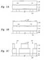
- FIGS. 1A-Gare cross sectional views of a substrate having the steps of the invention formed thereon.
- a silicon carbide barrier layer 110is deposited on the substrate surface to eliminate inter-level diffusion between the substrate and subsequently deposited material.
- the substrate surfacemay comprise metal features 107 formed in a dielectric material 105 .
- the silicon carbide barrier layer 110may be doped with oxygen, boron, phosphorus, or combinations thereof.
- a first dielectric layer 112comprising silicon, oxygen, and carbon, as described herein is deposited on the silicon carbide barrier layer 110 on the substrate surface including metal features 107 formed in a dielectric material 105 .
- the first dielectric layer 112 of interlayer dielectric materialis deposited on the first silicon carbide barrier layer 110 by oxidizing an organosilane or organosiloxane, such as trimethylsilane, to a thickness of about 5,000 to about 15,000 ⁇ , depending on the size of the structure to be fabricated.
- the first dielectric layermay also comprise other low k dielectric material such as a low k polymer material including paralyne or a low k spin-on glass such as un-doped silicon glass (USG) or fluorine-doped silicon glass (FSG).
- a plasma process following deposition as described herein for the silicon oxycarbide layermay then treat the first dielectric layer 112 .
- a low k etch stop (or second barrier layer) 114 of a silicon carbide material or oxidized organo silane layeris then deposited on the first dielectric layer 112 to a thickness of about 200 to about 1000 ⁇ .
- the etch stop 114may be a nitrogen containing silicon carbide material.
- the low k etch stop 114is then pattern etched to define the contact/via openings 116 and to expose first dielectric layer 112 in the areas where the contacts/vias are to be formed as shown in FIG. 1 A.
- the low k etch stop 114is pattern etched using conventional photolithography and etch processes using fluorine, carbon, and oxygen ions. While not shown, a nitrogen-free silicon carbide or silicon oxide cap layer between about 100 ⁇ and about 500 ⁇ thick may be deposited on the etch stop 116 prior to depositing further materials.
- a second dielectric layer 118 of silicon oxycarbide as described hereinis deposited to a thickness of about 5,000 to about 15,000 ⁇ as shown in FIG. 1 A.
- the second dielectric layer 118may also be plasma treated as described herein for the silicon oxycarbide layer.
- a nitrogen-free silicon carbide or silicon oxide cap layer between about 100 ⁇ and about 500 ⁇ thickmay be deposited on second dielectric layer 118 prior to depositing additional materials, such as photoresist materials.
- a silicon carbide cap layer(not shown) may be deposited on the second dielectric layer 118 prior to depositing additional materials, such as photoresist materials.
- An amorphous carbon layer 122is then deposited on the second dielectric layer 118 (or cap layer) and patterned preferably using conventional photolithography processes to define the interconnect lines 120 as shown in FIG. 1 B.
- the amorphous carbon layer 122is deposited as described herein.
- the amorphous carbon layerhas a thickness in the range of about 50 ⁇ to about 1000 ⁇ .
- the amorphous carbon layer 122is a hardmask which may perform as a stop for chemical mechanical polishing techniques to allow removal of conductive material while protecting low k dielectric materials, such as the second dielectric layer 118 , from damage during etching or from polishing methods.
- the featuresare then etched through the second dielectric layer 118 , the low k etch stop 114 , the first dielectric layer 112 , and the silicon carbide barrier layer 110 as shown in FIG. 1 C.
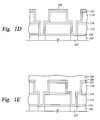
- the interconnect lines 120are filed to form a metallization structure with a conductive material such as aluminum, copper, tungsten or combinations thereof.
- a suitable barrier layer 124such as tantalum or tantalum nitride is first deposited conformally in the metallization pattern to prevent copper migration into the surrounding silicon and/or dielectric material.
- copper 126is deposited using either chemical vapor deposition, physical vapor deposition, electroplating, or combinations thereof to fill the structure as shown in FIG. 1 E.
- the amorphous carbon layerhas a selectivity, or removal rate ratio, of conductive material, either copper or barrier layer materials, to amorphous carbon of greater than about 1:1, such as between about 5:1 and about 30:1, and can include removal rate ratios of greater than 30:1.
- the amorphous carbon layer 122is then exposed to a plasma of a hydrogen-containing gas to remove the amorphous containing material from the surface of the substrate.
- a hydrogen-containing plasma removal processmay be performed by introducing hydrogen gas at a flow rate of about 1000 sccm, maintaining a chamber pressure of about 5 Torr, maintaining a substrate temperature at about 250° C., generating a plasma by supplying a RF power level of between about 100 W and about 300 W for a 200 mm substrate, and maintaining the plasma for about 60 seconds, or as necessary to remove the amorphous carbon material.
- the gas distributoris positioned about 500 mils from the substrate surface during the plasma treatment.
Landscapes
- Engineering & Computer Science (AREA)
- Physics & Mathematics (AREA)
- Condensed Matter Physics & Semiconductors (AREA)
- General Physics & Mathematics (AREA)
- Manufacturing & Machinery (AREA)
- Computer Hardware Design (AREA)
- Microelectronics & Electronic Packaging (AREA)
- Power Engineering (AREA)
- Plasma & Fusion (AREA)
- Chemical & Material Sciences (AREA)
- Chemical Kinetics & Catalysis (AREA)
- General Chemical & Material Sciences (AREA)
- Inorganic Chemistry (AREA)
- Internal Circuitry In Semiconductor Integrated Circuit Devices (AREA)
- Chemical Vapour Deposition (AREA)
- Formation Of Insulating Films (AREA)
Abstract
Description
This application is related to co-pending U.S. patent application Ser. No. 09/590,322 (AMAT/4227), filed on Jun. 8, 2000, and co-pending U.S. patent application Ser. No. 09/921,938 (AMAT/4227.P1), filed on Aug. 2, 2001.
1. Field of the Invention
The invention relates to the fabrication of integrated circuits and to a process for depositing dielectric layers on a substrate and the structures formed by the dielectric layer.
2. Description of the Related Art
One of the primary steps in the fabrication of modern semiconductor devices is the formation of metal and dielectric layers on a substrate by chemical reaction of gases. Such deposition processes are referred to as chemical vapor deposition or CVD. Conventional thermal CVD processes supply reactive gases to the substrate surface where heat-induced chemical reactions take place to produce a desired layer.
Semiconductor device geometries have dramatically decreased in size since such devices were first introduced several decades ago. Since then, integrated circuits have generally followed the two year/half-size rule (often called Moore's Law), which means that the number of devices that will fit on a chip doubles every two years. Today's fabrication plants are routinely producing devices having 0.35 μm and even 0.18 μm feature sizes, and tomorrow's plants soon will be producing devices having even smaller geometries.
To further reduce the size of devices on integrated circuits, it has become necessary to use conductive materials having low resistivity and to use insulators having low dielectric constants (dielectric constant (k)<4.0) to also reduce the capacitive coupling between adjacent metal lines. One such low k material is silicon oxycarbide deposited by a chemical vapor deposition process and silicon carbide, both of which may be used as dielectric materials in fabricating damascene features.
One conductive material having a low resistivity is copper and its alloys, which have become the materials of choice for sub-quarter-micron interconnect technology because copper has a lower resistivity than aluminum, (1.7 μΩ-cm compared to 3.1 μΩ-cm for aluminum), a higher current and higher carrying capacity. These characteristics are important for supporting the higher current densities experienced at high levels of integration and increased device speed. Further, copper has a good thermal conductivity and is available in a highly pure state.
One difficulty in using copper in semiconductor devices is that copper is difficult to etch and achieve a precise pattern. Etching with copper using traditional deposition/etch processes for forming interconnects has been less than satisfactory. Therefore, new methods of manufacturing interconnects having copper containing materials and low k dielectric materials are being developed.
One method for forming vertical and horizontal interconnects is by a damascene or dual damascene method. In the damascene method, one or more dielectric materials, such as the low k dielectric materials, are deposited and pattern etched to form the vertical interconnects, e.g., vias, and horizontal interconnects, e.g., lines. Conductive materials, such as copper containing materials, and other materials, such as barrier layer materials used to prevent diffusion of copper containing materials into the surrounding low k dielectric, are then inlaid into the etched pattern. Any excess copper containing materials and excess barrier layer material external to the etched pattern, such as on the field of the substrate, is then removed.
However, when low k material have been used in damascene formation, it has been difficult to produced features with little or no surface defects or feature deformation. It as been observed that low k dielectric materials are often porous and susceptible to being scratched and damaged during removal of conductive materials, which results in surface defects being formed on the substrate surface. Further, low k materials are often brittle and may deform under conventional polishing processes. One solution to limiting or reducing surface defects and deformation is to deposit a hardmask over the exposed low k materials prior to patterning and etching feature definitions in the low k materials. The hardmask is resistive to damage and deformation. The hardmask protects the underlying low k materials during subsequent material deposition and planarization or material removal processes, such as chemical mechanical polishing techniques or etching techniques, to reduce defect formation and feature deformation. The hardmask may then be removed following planarization prior to subsequent processing of the substrate.
One material of interest as a hardmask is amorphous carbon. Amorphous carbon has a low dielectric constant (i.e., k<4) and a sufficiently high resistance to removal from etching and polishing techniques to perform as a hardmask. However, hardmask removal processes comprise plasma-stripping processes containing oxygen, etching gases, such as CF4, and inert gases. The underlying low k material is sensitive to damage from etching gases and inert gases during the stripping processes and is sensitive to oxygen contamination, which may result in surface defects in the underlying low k material as well as an increase in the dielectric constant of the low k material from oxygen contamination. Thus, such hardmask removal processes have been observed to produce dielectric stacks having a higher than desired dielectric constant.
Therefore, there remains a need for an improved process for depositing and removing layers disposed on low k dielectric materials with minimal effect of dielectric constants.
Aspects of the invention generally provide a method for removing one or more amorphous carbon layers disposed on a low k dielectric material with minimal or reduced defect formation and with minimal change in the dielectric constant of the low k dielectric material. In one aspect, the invention provides a method for processing a substrate including depositing at least one dielectric layer on a substrate surface, wherein the dielectric layer comprises silicon, oxygen, and carbon and has a dielectric constant of about 3 or less, forming one or more amorphous carbon layers on the at least one dielectric layer, and removing the one or more amorphous carbon layers by exposing the one or more amorphous carbon layers to a plasma of a hydrogen-containing gas.
In another aspect of the invention, a method is provided for processing a substrate including depositing at least one dielectric layer on a substrate surface, wherein the dielectric layer comprises silicon, oxygen, and carbon and has a dielectric constant of about 3 or less, forming one or more amorphous carbon layers on the at least one dielectric layer by providing a gas mixture to the deposition chamber, wherein the gas mixture comprises one or more hydrocarbon compounds have the general formula CxHy, wherein x has a range of 2 to 4 and y has a range of 2 to 10, and an inert gas and generating a plasma of the gas mixture to disassociate the one or more hydrocarbon compounds in the gas mixture to form an amorphous carbon layer on the substrate, and removing the one or more amorphous carbon layers by exposing the one or more amorphous carbon layers to a plasma of a hydrogen-containing gas.
In another aspect of the invention, a method is provided for processing a substrate depositing at least one dielectric layer on a substrate surface, wherein the dielectric layer comprises silicon, oxygen, and carbon and has a dielectric constant of about 3 or less, forming one or more amorphous carbon layers on the at least one dielectric layer, defining a pattern in at least one region of the one or more amorphous carbon layers, forming feature definitions in the at least one dielectric layer by the patter n formed in the at least one region of the one or more amorphous carbon layers, depositing one or more conductive materials in the feature definitions, polishing the one or more conductive materials and stopping on the one or more amorphous carbon layers, and removing the one or more amorphous carbon layers by exposing the one or more amorphous carbon layers to a plasma of a hydrogen-containing gas.
So that the manner in which the above features of the invention are attained and can be understood in detail, a more particular description of the invention, briefly summarized above, may be had by reference to the embodiments thereof which are illustrated in the appended drawings.
It is to be noted, however, that the appended drawings illustrate only typical embodiments of this invention and are therefore not to be considered limiting of its scope, for the invention may admit to other equally effective embodiments.
FIGS. 1A-1G are cross sectional views showing one embodiment of a dual damascene deposition sequence of the invention;
For a further understanding of aspect of the invention, reference should be made to the ensuing detailed description.
Aspects of the invention generally provide a method for removing amorphous carbon material disposed on a low k dielectric material with minimal or reduced defect formation and minimal change in the dielectric constant of the low k dielectric material. The words and phrases used herein should be given their ordinary and customary meaning in the art by one skilled in the art unless otherwise further defined.
The amorphous carbon material may be removed by exposing the amorphous carbon material to a plasma of a hydrogen-containing gas. Low k material surfaces observed after removal of the amorphous carbon layer by the hydrogen-containing plasma have reduced surface defects compared to other removal processes with minimal change in the dielectric constant of the low k dielectric material thereunder.
The low k dielectric layer may be a silicon, oxygen, and carbon containing layer, such as a silicon oxycarbide layer. The silicon oxycarbide layer generally comprises between about 15 atomic % or greater of oxygen in the layer. The silicon oxycarbide layer may also contain hydrogen, nitrogen, or combinations thereof. The silicon oxycarbide layer is deposited by reacting an organosilicon compound to form a dielectric layer comprising carbon-silicon bonds and a dielectric constant less than about 3.
Suitable organosilane compounds include aliphatic organosilicon compounds, cyclic organosilicon compounds, or combinations thereof. Cyclic organosilicon compounds typically have a ring comprising three or more silicon atoms and the ring may further comprise one or more oxygen atoms. Commercially available cyclic organosilicon compounds include rings having alternating silicon and oxygen atoms with one or two alkyl groups bonded to the silicon atoms.
Aliphatic organosilicon compounds have linear or branched structures comprising one or more silicon atoms and one or more carbon atoms, and the structure may further comprise oxygen. Commercially available aliphatic organosilicon compounds include organosilanes that do not contain oxygen between silicon atoms and organosiloxanes that contain oxygen between two or more silicon atoms.
The carbon content of the deposited layers refers to atomic analysis of the layer structure that typically does not contain significant amounts of non-bonded hydrocarbons. The carbon contents are represented by the percent of carbon atoms in the deposited layer, excluding hydrogen atoms that are difficult to quantify. For example, a layer having an average of one silicon atom, one oxygen atom, one carbon atom, and two hydrogen atoms has a carbon content of 20 atomic percent (one carbon atom per five total atoms), or a carbon content of 33 atomic percent excluding hydrogen atoms (one carbon atom per three total atoms).
Organosilicon compounds contain carbon atoms in organic groups. Low dielectric constant layers are prepared from organosilicon compounds that have one or more carbon atoms attached to silicon wherein the carbon is not readily removed by oxidation at suitable processing conditions. Organic groups may include alkyl, alkenyl, cyclohexenyl, and aryl groups in addition to functional derivatives thereof.
Cyclic organosilicon compounds include, for example, one or more of the following compounds:
| 1,3,5-trisilano- | —(—SiH2CH2—)3— (cyclic) |
| 2,4,6-trimethylene, | |
| 1,3,5,7- | —(—SiHCH3—O—)4— (cyclic) |
| tetramethylcyclotetra- | |
| siloxane (TMCTS) | |
| Octamethylcyclotetra- | —(—Si(CH3)2—O—)4— (cyclic) |
| siloxane (OMCTS), | |
| 2,4,6,8,10- | —(—SiHCH3—O—)5— (cyclic) |
| pentamethylcyclopenta- | |
| siloxane, | |
| 1,3,5,7-tetrasilano- | —(—SiH2—CH2—SiH2—O—)2— (cyclic) |
| 2,6-dioxy-4,8-dimethylene, | |
| Hexamethylcyclotrisiloxane | —(—Si(CH3)2—O—)3— (cyclic) |
Aliphatic organosilicon compounds include for example, one or more of the following compounds:
| Methylsilane, | CH3—SiH3 |
| Dimethylsilane, | (CH3)2—SiH2 |
| Trimethylsilane, | (CH3)3—SiH |
| Dimethyldimethoxysilane, | (CH3)2—Si—(OCH3)2 |
| Ethylsilane, | CH3—CH2—SiH3 |
| Disilanomethane, | SiH3—CH2—SiH3 |
| bis(methylsilano)methane, | CH3—SiH2—CH2—SiH2—CH3 |
| 1,2-disilanoethane, | SiH3—CH2—CH2—SiH3 |
| 1,2-bis(methylsilano)ethane, | CH3—SiH2—CH2—CH2—SiH2—CH3 |
| 2,2-disilanopropane, | SiH3—C(CH3)2—SiH3 |
| 1,3-dimethyldisiloxane, | CH3—SiH2—O—SiH2—CH3 |
| 1,1,3,3-tetramethyldisiloxane, | (CH3)2—SiH—O—SiH—(CH3)2 |
| Hexamethyldisiloxane (HMDS), | (CH3)3—Si—O—Si—(CH3)3 |
| 1,3-bis(silanomethylene) | (SiH3—CH2—SiH2—)2—O |
| disiloxane, | |
| bis(1-methyldisiloxanyl) | (CH3—SiH2—O—SiH2—)2—CH2 |
| methane, | |
| 2,2-bis(1-methyldisiloxanyl) | (CH3—SiH2—O—SiH2—)2—C(CH3)2, |
| propane, | and |
| Hexamethoxydisiloxane | (CH3O)3—Si—O—Si—(OCH3)3. |
| (HMDOS) | |
The above list is illustrative and should not be construed or interpreted as limiting the scope of the invention.
In one aspect, a cyclic organosilicon compound and an aliphatic organosilicon compound are reacted with an oxidizing gas in amounts sufficient to deposit a low dielectric constant layer on a semiconductor substrate, wherein the cyclic organosilicon compound comprises at least one silicon-carbon bond. The aliphatic organosilicon compound contains a silicon-hydrogen bond or a silicon-oxygen bond, preferably a silicon-hydrogen bond. For example, the cyclic organosilicon compound may be 1,3,5,7-tetramethylcyclotetrasiloxane or octamethylcyclotetrasiloxane and the aliphatic organosilicon compound may be trimethylsilane or 1,1,3,3-tetramethyldisiloxane.
In another aspect, both the cyclic organosilicon compound and the aliphatic organosilicon compound contain a silicon-hydrogen bond. For example, 1,3,5,7-tetramethylcyclotetrasiloxane and trimethylsilane or 1,1,3,3-tetramethyldisiloxane are blended and oxidized while applying RF power.
Generally, the organosilicon compounds are reacted in a plasma comprising a relatively inert gas, preferably a noble gas, such as helium or argon, or nitrogen (N2). The deposited silicon oxycarbide layers may have dielectric constants of about 3 or less.
A preferred silicon, oxygen, and carbon layer is deposited in one embodiment by supplying trimethylsilane or 1,3,5,7-tetramethylcyclotetrasiloxane to a plasma processing chamber at a flow rate between about 10 and about 1000 standard cubic centimeters per minute (sccm) with an oxidizing gas supplied to the processing chamber at a flow rate between about 10 sccm and about 1000 sccm. An inert gas, such as helium, argon, or combinations thereof, is also supplied to the chamber at a flow rate between about 50 sccm and about 5000 sccm. The chamber pressure is maintained between about 100 milliTorr and about 15 Torr. The substrate surface temperature is maintained between about 100° C. and about 450° C. during the deposition process.
The organosilicon compound, the oxidizing gas, and the inert gas, are introduced to the processing chamber via a gas distribution plate spaced between about 200 millimeters (mm) and about 600 millimeters from the substrate on which the silicon carbide layer is being deposited upon. Power from a single 13.56 MHz RF power source is supplied to the chamber 10 to form the plasma at a power density between about 0.3 watts/cm2and about 3.2 watts/cm2, or a power level between about 100 watts and about 1000 watts for a 200 mm substrate. A power density between about 0.9 watts/cm2and about 2.3 watts/cm2, or a power level between about 300 watts and about 700 watts for a 200 mm substrate, is preferably supplied to the processing chamber to generate the plasma.
The organosilicon compounds are oxidized during deposition of the silicon oxycarbide layer, preferably by reaction with oxygen (O2), ozone (O3), nitrous oxide (N2O), carbon monoxide (CO), carbon dioxide (CO2), water (H2O), or combinations thereof. When ozone is used as an oxidizing gas, an ozone generator typically converts about 15 wt. % of the oxygen in a source gas to ozone, with the remainder typically being oxygen. However, the ozone concentration may be increased or decreased based upon the amount of ozone desired and the type of ozone generating equipment used. Organosilicon compounds that contain oxygen may be disassociated to provide the oxygen. During deposition of the silicon oxycarbide layer, the substrate is maintained at a temperature between about −20° C. and about 500° C., and preferably is maintained at a temperature between about 170° C. and about 180° C.
For a plasma enhanced deposition of the silicon oxycarbide layer, the organosilicon material is deposited using a power density ranging between about 0.03 W/cm2and about 6.4 W/cm2, which is a RF power level of between about 10 W and about 2000 W for a 200 mm substrate. Preferably, the RF power level is between about 300 W and about 1700 W. The RF power is provided at a frequency between about 0.01 MHz and 300 MHz. The RF power may be provided continuously or in short duration cycles wherein the power is on at the stated levels for cycles less than about 200 Hz and the on cycles total between about 10% and about 50% of the total duty cycle. The deposition process of the low dielectric constant layer is performed in a substrate processing system described in more detail below. The silicon oxycarbide layer can be deposited continuously or with interruptions, such as changing chambers or providing cooling time, to improve porosity.
In one embodiment of plasma enhanced deposition, oxygen or oxygen containing compounds are dissociated to increase reactivity and achieve desired oxidation of the deposited layer. RF power is coupled to the deposition chamber to increase dissociation of the compounds. The compounds may also be dissociated in a microwave chamber prior to entering the deposition chamber.
Following deposition, the deposited dielectric material may be annealed at a temperature between about 100° C. and about 400° C. for between about 1 minute and about 60 minutes, preferably at about 30 minutes, to reduce the moisture content and increase the solidity and hardness of the dielectric material, if desired. The anneal is preferably performed after the deposition of the next layer which prevents shrinkage or deformation of the dielectric layer. Inert gases, such as argon and helium, may be added to the annealing atmosphere.
The deposited silicon oxycarbide layer may also be plasma treated prior to deposition of photoresist materials thereon. The plasma treatment is believed to remove a portion of the carbon material from the surface of the silicon oxycarbide layer or silicon carbide layer that reduces the surface's reactivity to subsequently deposited materials. The plasma treatment may be performed in the same chamber used to deposit the silicon and carbon containing material.
The plasma treatment generally includes providing an inert gas including helium, argon, neon, xenon, krypton, or combinations thereof, to a processing chamber at a flow rate between about 500 sccm and about 3000 sccm, and generating a plasma in the processing chamber. The plasma may be generated using a power density ranging between about 0.03 W/cm2and about 3.2 W/cm2, which is a RF power level of between about 10 W and about 1000 W for a 200 mm substrate. Preferably, a power level of between about 200 watts and about 800 watts is used in depositing the silicon carbide material for a 200 mm substrate. The RF power can be provided at a high frequency such as between 13 MHz and 14 MHz. The RF power can be provided continuously or in short duration cycles wherein the power is on at the stated levels for cycles less than about 200 Hz and the on cycles total between about 10% and about 30% of the total duty cycle.
The processing chamber is generally maintained at a chamber pressure of between about 3 Torr and about 12 Torr. A chamber pressure between about 7 Torr and about 10 Torr. The substrate is maintained at a temperature between about 300° C. and about 450° C. during the plasma treatment. A substrate temperature between about 350° C. and about 400° C. may be used during the plasma treatment. The plasma treatment may be performed between about 10 seconds and about 100 seconds, with a plasma treatment between about 40 seconds and about 60 seconds preferably used.
The processing gas may be introduced into the chamber by a gas distributor, the gas distributor may be positioned between about 200 mils and about 500 mils from the substrate surface. The showerhead may be positioned between about 300 mils and about 400 mils during the plasma treatment. However, it should be noted that the respective parameters may be modified to perform the plasma processes in various chambers and for different substrate sizes, such as 300 mm substrates.
Alternatively, a silicon carbide layer may be deposited with the silicon oxycarbide layer. The silicon carbide layer is a dielectric material having a dielectric constant (k) of about 6 or less. The silicon carbide material may be deposited before or after deposition of the silicon oxycarbide material, and may be used as a barrier layer, an etch stop, or an antireflective coating.
An amorphous carbon layer is then deposited on the low k dielectric material. In one embodiment, a gas mixture of a hydrocarbon compound, and, optionally, an inert gas, such as argon (Ar) or helium (He), is introduced into a processing chamber. The hydrocarbon compound has a formula CxHy, where x has a range of between 2 and 4 and y has a range of between 2 and 10. For example, propylene (C3H6), propyne (C3H4), propane (C3H8), butane (C4H10), butylene (C4H8), butadiene (C4H6), or acetelyne (C2H2) as well as combinations thereof, may be used as the hydrocarbon compound. Alternatively, partially or completely fluorinated derivatives of the hydrocarbon compounds, for example, C3F8or C4F8, may be used to deposit a fluorinated amorphous carbon layer, which may be described as an amorphous fluorocarbon layer. A combination of hydrocarbon compounds and fluorinated derivatives of hydrocarbon compounds may be used to deposit the amorphous carbon layer or amorphous fluorocarbon layer.
Similarly, a variety of gases such as hydrogen (H2), nitrogen (N2), ammonia (NH3), or combinations thereof, among others, may be added to the gas mixture to modify properties of the amorphous carbon material. Argon, helium, and nitrogen are used to control the density and deposition rate of the amorphous carbon layer.
The addition of H2and/or NH3can be used to control the hydrogen ratio of the amorphous carbon layer to control layer properties, such as reflectivity.
The amorphous carbon layer is then deposited from the processing gas using the following deposition process parameters. The substrate is maintained at a substrate temperature between about 100° C. and about 500° C., a chamber pressure is maintained between about 1 Torr and about 20 Torr, the hydrocarbon gas (CxHy) has a flow rate between about 50 sccm and about 500 sccm for a 200 mm substrate, a plasma is generated by applying a RF power of between about 3 W/cm2and about 20 W/cm2, or between about 1000 watts (w) and about 6000 W for a 200 mm substrate, with a gas distributor being between about 300 mils and about 600 mils from the substrate surface. The above process parameters provide a typical deposition rate for the amorphous carbon layer in the range of about 100 Å/min to about 1000 Å/min and can be implemented on a 200 mm substrate in a deposition chamber, such as the DxZ™ processing chamber commercially available from Applied Materials, Inc. The applied RF power may be varied based upon the substrate size and the equipment used, for example, the applied RF power may be between about 19 W/cm2and about 130 W/cm2. The amorphous carbon deposition values provided herein are illustrative and should not be construed as limiting the scope of the invention.
The amorphous carbon layer comprises carbon and hydrogen atoms, which may be an adjustable carbon:hydrogen ratio that ranges from about 10% hydrogen to about 60% hydrogen. Controlling the hydrogen ratio of the amorphous carbon layer is desirable for tuning the respective optical properties, etch selectivity and chemical mechanical polishing resistance properties. Specifically, as the hydrogen content decreases the optical properties of the as-deposited layer such as for example, the index of refraction (n) and the absorption coefficient (k) increase. Similarly, as the hydrogen content decreases the etch resistance of the amorphous carbon layer increases.
The light absorption coefficient, k, of the amorphous carbon layer can be varied between about 0.1 to about 1.0 at wavelengths below about 250 nm, such as between about 193 nm and about 250 nm, making the amorphous carbon layer suitable for use as an anti-reflective coating (ARC) at DUV wavelengths. The absorption coefficient of the amorphous carbon layer can be varied as a function of the deposition temperature. In particular, as the temperature increases the absorption coefficient of the as-deposited layer likewise increases. For example, when propylene is the hydrocarbon compound the k value for the as-deposited amorphous carbon layers can be increased from about 0.2 to about 0.7 by increasing the deposition temperature from about 150° C. to about 480° C.
The absorption coefficient of the amorphous carbon layer can also be varied as a function of the additive used in the gas mixture. In particular, the presence of hydrogen (H2), ammonia (NH3), and nitrogen (N2), or combinations thereof, in the gas mixture can increase the k value by about 10% to about 100%. The amorphous carbon layer is further described in U.S. patent application Ser. No. 09/590,322, filed on Jun. 8, 2000, entitled, “Method for Depositing an Amorphous Carbon Layer”, which is incorporated herein to the extent not inconsistent with the claimed aspects and description herein.
Removal of the amorphous carbon material from the low k dielectric material may be achieved by subjecting the amorphous carbon layer to a plasma of a hydrogen-containing gas. The plasma of the hydrogen-containing gas is believed to remove the amorphous carbon material with minimal change on the dielectric constant of the low k material disposed thereunder and reduced or minimal surface defect formation.
The plasma treatment generally includes providing the hydrogen containing gas including hydrogen, ammonia, water vapor (H2O), or combinations thereof, to a processing chamber at a flow rate between about 100 sccm and about 1000 sccm, preferably between about 500 sccm and about 1000 sccm, and generating a plasma in the processing chamber. The plasma may be generated using a power density ranging between about 0.15 W/cm2and about 5 W/cm2, which is a RF power level of between about 50 W and about 1500 W for a 200 mm substrate. The RF power can be provided at a high frequency such as between 13 MHz and 14 MHz. The RF power can be provided continuously or in short duration cycles wherein the power is on at the stated levels for cycles less than about 200 Hz and the on cycles total between about 10% and about 30% of the total duty cycle.
The processing chamber is generally maintained at a chamber pressure of between about 1 Torr and about 10 Torr, preferably between about 3 Torr and about 8 Torr. The substrate is maintained at a temperature between about 100° C. and about 300° C. during the plasma treatment, preferably, between about 200° C. and about 300° C. The plasma treatment may be performed between about 15 seconds and about 120 seconds, or as necessary to remove the amorphous carbon material. The processing gas may be introduced into the chamber by a gas distributor, the gas distributor may be positioned between about 100 mils and about 2000 mils from the substrate surface, preferably positioned between about 200 mils and about 1000 mils, during the plasma treatment. However, it should be noted that the respective parameters may be modified to perform the plasma processes in various chambers and for different substrate sizes, such as 300 mm substrates.
A suitable reactor for performing the low k deposition, the amorphous carbon material deposition, and the hydrogen-containing gas plasma removal of the amorphous carbon materials described herein may be performed in a DxZ™ chemical vapor deposition chamber commercially available from Applied Materials, Inc., Santa Clara, Calif.
Deposition of a Dual Damascene Structure
An example of a damascene structure that is formed using the low k dielectric silicon, oxygen, and carbon material, the amorphous carbon material, and the amorphous carbon material removal process described herein is shown in FIGS. 1A-G, which are cross sectional views of a substrate having the steps of the invention formed thereon.
As shown in FIG. 1 A, a siliconcarbide barrier layer 110 is deposited on the substrate surface to eliminate inter-level diffusion between the substrate and subsequently deposited material. The substrate surface may comprise metal features107 formed in adielectric material 105. The siliconcarbide barrier layer 110 may be doped with oxygen, boron, phosphorus, or combinations thereof.
Afirst dielectric layer 112, comprising silicon, oxygen, and carbon, as described herein is deposited on the siliconcarbide barrier layer 110 on the substrate surface including metal features107 formed in adielectric material 105. Thefirst dielectric layer 112 of interlayer dielectric material is deposited on the first siliconcarbide barrier layer 110 by oxidizing an organosilane or organosiloxane, such as trimethylsilane, to a thickness of about 5,000 to about 15,000 Å, depending on the size of the structure to be fabricated.
An example of a low dielectric constant material that may be used as an interlayer dielectric material is Black Diamond ® dielectric material commercially available from Applied Materials, Inc., of Santa Clara, Calif. Alternatively, the first dielectric layer may also comprise other low k dielectric material such as a low k polymer material including paralyne or a low k spin-on glass such as un-doped silicon glass (USG) or fluorine-doped silicon glass (FSG). A plasma process following deposition as described herein for the silicon oxycarbide layer may then treat thefirst dielectric layer 112.
A low k etch stop (or second barrier layer)114 of a silicon carbide material or oxidized organo silane layer is then deposited on thefirst dielectric layer 112 to a thickness of about 200 to about 1000 Å. Alternatively, the etch stop114 may be a nitrogen containing silicon carbide material. The lowk etch stop 114 is then pattern etched to define the contact/viaopenings 116 and to expose firstdielectric layer 112 in the areas where the contacts/vias are to be formed as shown in FIG.1A. Preferably, the lowk etch stop 114 is pattern etched using conventional photolithography and etch processes using fluorine, carbon, and oxygen ions. While not shown, a nitrogen-free silicon carbide or silicon oxide cap layer between about 100 Å and about 500 Å thick may be deposited on the etch stop116 prior to depositing further materials.
After the lowk etch stop 114 has been etched to pattern the contacts/vias and the photoresist has been removed, asecond dielectric layer 118 of silicon oxycarbide as described herein is deposited to a thickness of about 5,000 to about 15,000 Å as shown in FIG.1A. Thesecond dielectric layer 118 may also be plasma treated as described herein for the silicon oxycarbide layer.
In an alternative embodiment, a nitrogen-free silicon carbide or silicon oxide cap layer between about 100 Å and about 500 Å thick may be deposited on seconddielectric layer 118 prior to depositing additional materials, such as photoresist materials. In a further alternative embodiment, a silicon carbide cap layer (not shown) may be deposited on thesecond dielectric layer 118 prior to depositing additional materials, such as photoresist materials.
Anamorphous carbon layer 122 is then deposited on the second dielectric layer118 (or cap layer) and patterned preferably using conventional photolithography processes to define theinterconnect lines 120 as shown in FIG.1B. Theamorphous carbon layer 122 is deposited as described herein. Typically, the amorphous carbon layer has a thickness in the range of about 50 Å to about 1000 Å.
Theamorphous carbon layer 122 is a hardmask which may perform as a stop for chemical mechanical polishing techniques to allow removal of conductive material while protecting low k dielectric materials, such as thesecond dielectric layer 118, from damage during etching or from polishing methods.
The features are then etched through thesecond dielectric layer 118, the lowk etch stop 114, thefirst dielectric layer 112, and the siliconcarbide barrier layer 110 as shown in FIG.1C. The interconnect lines120 are filed to form a metallization structure with a conductive material such as aluminum, copper, tungsten or combinations thereof. Presently, the trend is to use copper to form the smaller features due to the low resistivity of copper (1.7 mW-cm compared to 3.1 mW-cm for aluminum). Preferably, as shown in FIG. 1D, asuitable barrier layer 124 such as tantalum or tantalum nitride is first deposited conformally in the metallization pattern to prevent copper migration into the surrounding silicon and/or dielectric material. Thereafter,copper 126 is deposited using either chemical vapor deposition, physical vapor deposition, electroplating, or combinations thereof to fill the structure as shown in FIG.1E.
Once the structure has been filled with copper or other metal, the surface is planarized using chemical mechanical polishing to remove anyexcess copper 126 andbarrier layer 124 materials. However, the polishing resistantamorphous carbon layer 122 remains behind after the polishing process as shown in FIG.1F. The amorphous carbon layer has a selectivity, or removal rate ratio, of conductive material, either copper or barrier layer materials, to amorphous carbon of greater than about 1:1, such as between about 5:1 and about 30:1, and can include removal rate ratios of greater than 30:1.
Theamorphous carbon layer 122 is then exposed to a plasma of a hydrogen-containing gas to remove the amorphous containing material from the surface of the substrate. An example of the hydrogen-containing plasma removal process may be performed by introducing hydrogen gas at a flow rate of about 1000 sccm, maintaining a chamber pressure of about 5 Torr, maintaining a substrate temperature at about 250° C., generating a plasma by supplying a RF power level of between about 100 W and about 300 W for a 200 mm substrate, and maintaining the plasma for about 60 seconds, or as necessary to remove the amorphous carbon material. The gas distributor is positioned about 500 mils from the substrate surface during the plasma treatment.
While the foregoing is directed to preferred embodiments of the present invention, other and further embodiments of the invention may be devised without departing from the basic scope thereof, and the scope thereof is determined by the claims that follow.
Claims (22)
1. A method for processing a substrate in a chamber, comprising:
depositing at least one dielectric layer on a substrate surface, wherein the dielectric layer comprises silicon, oxygen, and carbon and has a dielectric constant of about 3 or less;
forming one or more amorphous carbon layers on the at least one dielectric layer; and
removing the one or more amorphous carbon layers by exposing the one or more amorphous carbon layers to a plasma of a hydrogen-containing gas.
2. The method ofclaim 1 , wherein the forming one or more amorphous carbon layers comprises reacting one or more hydrocarbon compounds having the general formula CxHy, wherein x has a range of 2 to 4 and y has a range of 2 to 10.
3. The method ofclaim 2 , wherein the one or more hydrocarbon compounds are selected from the group consisting of propylene (C3H6), propyne (C3H4), propane (C3H8), butane (C4H10), butylene (C4H8), butadiene (C4H6), acetelyne (C2H2), and combinations thereof.
4. The method ofclaim 2 , further comprising generating a plasma when reacting the one or more hydrocarbon compounds.
5. The method ofclaim 1 , wherein the hydrogen-containing gas comprises a gas selected from the group of hydrogen, ammonia, water vapor, and combinations thereof.
6. The method ofclaim 1 , wherein the plasma is generated by applying a power level between about 0.15 watts/cm2and about 5 watts/cm2to the chamber.
7. The method ofclaim 6 , wherein the one or more amorphous carbon layers are exposed to the plasma for between about 10 seconds and about 120 seconds.
8. The method ofclaim 1 , wherein removing the one or more amorphous carbon layers comprises introducing a hydrogen-containing gas selected from the group of hydrogen, ammonia, water vapor, and combinations thereof, into the chamber at a flow rate of about 5000 sccm or less, maintaining the chamber at a pressure of between about 1 Torr and about 10 Torr, maintaining the substrate temperature between about 100° C. and about 300° C., generating the plasma by supplying a power level between about 50 watts and about 1500 watts to the processing chamber for a 200 mm substrate, and maintaining the plasma between about 10 seconds and about 120 seconds.
9. A method for processing a substrate, comprising:
depositing at least one dielectric layer on a substrate surface, wherein the dielectric layer comprises silicon, oxygen, and carbon and has a dielectric constant of about 3 or less;
forming one or more amorphous carbon layers on the at least one dielectric layer by providing a gas mixture to the deposition chamber and generating a plasma of the gas mixture to disassociate the one or more hydrocarbon compounds in the gas mixture, wherein the gas mixture comprises an inert gas and one or more hydrocarbon compounds have the general formula CxHy, wherein x has a range of 2 to 4 and y has a range of 2 to 10; and
removing the one or more amorphous carbon layers by exposing the one or more amorphous carbon layers to a hydrogen-containing plasma for between about 10 seconds and about 120 seconds.
10. The method ofclaim 9 , wherein the hydrogen containing plasma comprises a hydrogen-containing gas selected from the group of hydrogen, ammonia, water vapor, and combinations thereof.
11. The method ofclaim 10 , wherein the one or more hydrocarbon compounds are selected from the group consisting of propylene (C3H6), propyne (C3H4), propane (C3H8), butane (C4H10), butylene (C4H8), butadiene (C4H6), acetelyne (C2H2), and combinations thereof.
12. The method ofclaim 11 , wherein the one or more hydrocarbon compounds further comprises one or more fluorinated derivatives of the one or more hydrocarbon compounds.
13. The method ofclaim 9 , wherein removing the one or more amorphous carbon layers comprises introducing a hydrogen-containing gas selected from the group of hydrogen, ammonia, water vapor, and combinations thereof, into the chamber at a flow rate of about 5000 sccm or less, maintaining the chamber at a pressure of between about 1 Torr and about 10 Torr, maintaining the substrate temperature between about 100° C. and about 300° C., generating the plasma by supplying a power level between about 50 watts and about 1500 watts to the processing chamber for a 200 mm substrate, and maintaining the plasma between about 10 seconds and about 120 seconds.
14. A method for processing a substrate, comprising:
depositing at least one dielectric layer on a substrate surface, wherein the dielectric layer comprises silicon, oxygen, and carbon and has a dielectric constant of about 3 or less;
forming one or more amorphous carbon layers on the at least one dielectric layer;
defining a pattern in at least one region of the one or more amorphous carbon layers;
forming feature definitions in the at least one dielectric layer by the pattern formed in the at least one region of the one or more amorphous carbon layers;
depositing one or more conductive materials in the feature definitions;
polishing the one or more conductive materials and stopping on the one or more amorphous carbon layers; and
removing the one or more amorphous carbon layers by exposing the one or more amorphous carbon layers to a plasma of a hydrogen-containing gas.
15. The method ofclaim 14 , wherein the forming one or more amorphous carbon layers comprises reacting one or more hydrocarbon compounds having the general formula CxHy, wherein x has a range of 2 to 4 and y has a range of 2 to 10.
16. The method ofclaim 15 , wherein the one or more hydrocarbon compounds are selected from the group consisting of propylene (C3H6), propyne (C3H4), propane (C3H8), butane (C4H10), butylene (C4H8), butadiene (C4H6), acetelyne (C2H2), and combinations thereof.
17. The method ofclaim 15 , wherein the one or more hydrocarbon compounds further comprises one or more fluorinated derivatives of the one or more hydrocarbon compounds.
18. The method ofclaim 15 , further comprising generating a plasma when reacting the one or more hydrocarbon compounds.
19. The method ofclaim 14 , wherein the hydrogen-containing gas comprises a gas selected from the group of hydrogen, ammonia, water vapor, and combinations thereof.
20. The method ofclaim 17 , wherein the plasma is generated by applying a power level between about 0.15 watts/cm2and about 5 watts/cm2to the chamber for between about 10 seconds and about 120 seconds.
21. The method ofclaim 14 , wherein removing the one or more amorphous carbon layers comprises introducing a hydrogen-containing gas selected from the group of hydrogen, ammonia, water vapor, and combinations thereof, into the chamber at a flow rate of about 5000 sccm or less, maintaining the chamber at a pressure of between about 1 Torr and about 10 Torr, maintaining the substrate temperature between about 100° C. and about 300° C., generating the plasma by supplying a power level between about 50 watts and about 1500 watts to the processing chamber for a 200 mm substrate, and maintaining the plasma between about 10 seconds and about 120 seconds.
22. The method ofclaim 14 , wherein the one or more conductive materials and the one or more amorphous carbon layers are removed at a ratio of conductive materials to amorphous carbon of greater than about 1:1.
Priority Applications (4)
| Application Number | Priority Date | Filing Date | Title |
|---|---|---|---|
| US10/112,012US6541397B1 (en) | 2002-03-29 | 2002-03-29 | Removable amorphous carbon CMP stop |
| US10/383,839US6852647B2 (en) | 2002-03-29 | 2003-03-07 | Removable amorphous carbon CMP stop |
| US11/053,193US7148156B2 (en) | 2002-03-29 | 2005-02-08 | Removable amorphous carbon CMP stop |
| US11/594,626US7507677B2 (en) | 2002-03-29 | 2006-11-08 | Removable amorphous carbon CMP stop |
Applications Claiming Priority (1)
| Application Number | Priority Date | Filing Date | Title |
|---|---|---|---|
| US10/112,012US6541397B1 (en) | 2002-03-29 | 2002-03-29 | Removable amorphous carbon CMP stop |
Related Child Applications (1)
| Application Number | Title | Priority Date | Filing Date |
|---|---|---|---|
| US10/383,839ContinuationUS6852647B2 (en) | 2002-03-29 | 2003-03-07 | Removable amorphous carbon CMP stop |
Publications (1)
| Publication Number | Publication Date |
|---|---|
| US6541397B1true US6541397B1 (en) | 2003-04-01 |
Family
ID=22341664
Family Applications (4)
| Application Number | Title | Priority Date | Filing Date |
|---|---|---|---|
| US10/112,012Expired - Fee RelatedUS6541397B1 (en) | 2002-03-29 | 2002-03-29 | Removable amorphous carbon CMP stop |
| US10/383,839Expired - LifetimeUS6852647B2 (en) | 2002-03-29 | 2003-03-07 | Removable amorphous carbon CMP stop |
| US11/053,193Expired - Fee RelatedUS7148156B2 (en) | 2002-03-29 | 2005-02-08 | Removable amorphous carbon CMP stop |
| US11/594,626Expired - Fee RelatedUS7507677B2 (en) | 2002-03-29 | 2006-11-08 | Removable amorphous carbon CMP stop |
Family Applications After (3)
| Application Number | Title | Priority Date | Filing Date |
|---|---|---|---|
| US10/383,839Expired - LifetimeUS6852647B2 (en) | 2002-03-29 | 2003-03-07 | Removable amorphous carbon CMP stop |
| US11/053,193Expired - Fee RelatedUS7148156B2 (en) | 2002-03-29 | 2005-02-08 | Removable amorphous carbon CMP stop |
| US11/594,626Expired - Fee RelatedUS7507677B2 (en) | 2002-03-29 | 2006-11-08 | Removable amorphous carbon CMP stop |
Country Status (1)
| Country | Link |
|---|---|
| US (4) | US6541397B1 (en) |
Cited By (222)
| Publication number | Priority date | Publication date | Assignee | Title |
|---|---|---|---|---|
| US20020001778A1 (en)* | 2000-06-08 | 2002-01-03 | Applied Materials, Inc. | Photolithography scheme using a silicon containing resist |
| US20030091938A1 (en)* | 2000-02-17 | 2003-05-15 | Applied Materials, Inc. | Method of depositing an amorphous carbon layer |
| US20030186477A1 (en)* | 2002-03-29 | 2003-10-02 | Applied Materials, Inc. | Removable amorphous carbon CMP stop |
| US20040089924A1 (en)* | 2002-10-25 | 2004-05-13 | Matsushita Electric Industrial Co., Ltd. | Electronic device and method for fabricating the same |
| US20040121604A1 (en)* | 2002-12-18 | 2004-06-24 | Chun-Feng Nieh | Method of etching a low-k dielectric layer |
| US6780753B2 (en) | 2002-05-31 | 2004-08-24 | Applied Materials Inc. | Airgap for semiconductor devices |
| US20040185674A1 (en)* | 2003-03-17 | 2004-09-23 | Applied Materials, Inc. | Nitrogen-free hard mask over low K dielectric |
| US20040214446A1 (en)* | 2002-07-11 | 2004-10-28 | Applied Materials, Inc. | Nitrogen-free dielectric anti-reflective coating and hardmask |
| US6833625B1 (en)* | 2002-04-25 | 2004-12-21 | Advanced Micro Devices, Inc. | Self-aligned barrier formed with an alloy having at least two dopant elements for minimized resistance of interconnect |
| US20040259381A1 (en)* | 2003-06-18 | 2004-12-23 | Semiconductor Leading Edge Technologies, Inc. | Method for manufacturing semiconductor device |
| US20050026338A1 (en)* | 2003-07-28 | 2005-02-03 | Reber Douglas M. | Semiconductor device having an organic anti-reflective coating (ARC) and method therefor |
| US20050056835A1 (en)* | 2003-09-12 | 2005-03-17 | Micron Technology, Inc. | Transparent amorphous carbon structure in semiconductor devices |
| US20050056940A1 (en)* | 2003-09-12 | 2005-03-17 | Sandhu Gurtej S. | Masking structure having multiple layers including an amorphous carbon layer |
| US20050087870A1 (en)* | 2003-10-23 | 2005-04-28 | Adetutu Olubunmi O. | Semiconductor device and method of forming the same |
| US6893978B1 (en)* | 2002-12-03 | 2005-05-17 | Silicon Magnetic Systems | Method for oxidizing a metal layer |
| US20050124151A1 (en)* | 2003-12-04 | 2005-06-09 | Taiwan Semiconductor Manufacturing Co. | Novel method to deposit carbon doped SiO2 films with improved film quality |
| US20050167394A1 (en)* | 2004-01-30 | 2005-08-04 | Wei Liu | Techniques for the use of amorphous carbon (APF) for various etch and litho integration scheme |
| US20050184295A1 (en)* | 2004-02-24 | 2005-08-25 | Chartered Semiconductor Manufacturing Ltd. | Oxygen doped SiC for Cu barrier and etch stop layer in dual damascene fabrication |
| US20050202683A1 (en)* | 2004-03-12 | 2005-09-15 | Applied Materials, Inc. | Method of depositing an amorphous carbon film for etch hardmask application |
| US20050199013A1 (en)* | 2004-03-12 | 2005-09-15 | Applied Materials, Inc. | Use of amorphous carbon film as a hardmask in the fabrication of optical waveguides |
| US20050199585A1 (en)* | 2004-03-12 | 2005-09-15 | Applied Materials, Inc. | Method of depositing an amorphous carbon film for metal etch hardmask application |
| US20050208758A1 (en)* | 2002-12-16 | 2005-09-22 | Lsi Logic Corporation | Dielectric barrier films for use as copper barrier layers in semiconductor trench and via structures |
| US20050239002A1 (en)* | 2002-05-03 | 2005-10-27 | Weimin Li | Semiconductor multilevel interconnect structure |
| US20050287771A1 (en)* | 2004-03-05 | 2005-12-29 | Applied Materials, Inc. | Liquid precursors for the CVD deposition of amorphous carbon films |
| US20060014397A1 (en)* | 2004-07-13 | 2006-01-19 | Seamons Martin J | Methods for the reduction and elimination of particulate contamination with CVD of amorphous carbon |
| US20060051966A1 (en)* | 2004-02-26 | 2006-03-09 | Applied Materials, Inc. | In-situ chamber clean process to remove by-product deposits from chemical vapor etch chamber |
| US20060110938A1 (en)* | 2002-12-31 | 2006-05-25 | Lin Simon S | Etch stop layer |
| US20060154493A1 (en)* | 2005-01-10 | 2006-07-13 | Reza Arghavani | Method for producing gate stack sidewall spacers |
| US7105460B2 (en)* | 2002-07-11 | 2006-09-12 | Applied Materials | Nitrogen-free dielectric anti-reflective coating and hardmask |
| US20060222771A1 (en)* | 2004-07-13 | 2006-10-05 | Seamons Martin J | Methods for the reduction and elimination of particulate contamination with cvd of amorphous carbon |
| US20060292859A1 (en)* | 2005-06-27 | 2006-12-28 | Taiwan Semiconductor Manufacturing Co., Ltd. | Damascene process using dielectic layer containing fluorine and nitrogen |
| US20070128553A1 (en)* | 2005-10-19 | 2007-06-07 | Joerg Linz | Method for forming feature definitions |
| US20070202640A1 (en)* | 2006-02-28 | 2007-08-30 | Applied Materials, Inc. | Low-k spacer integration into CMOS transistors |
| US20070238254A1 (en)* | 2006-03-28 | 2007-10-11 | Applied Materials, Inc. | Method of etching low dielectric constant films |
| US20070286954A1 (en)* | 2006-06-13 | 2007-12-13 | Applied Materials, Inc. | Methods for low temperature deposition of an amorphous carbon layer |
| US7381644B1 (en) | 2005-12-23 | 2008-06-03 | Novellus Systems, Inc. | Pulsed PECVD method for modulating hydrogen content in hard mask |
| US7399712B1 (en) | 2005-10-31 | 2008-07-15 | Novellus Systems, Inc. | Method for etching organic hardmasks |
| US20080254233A1 (en)* | 2007-04-10 | 2008-10-16 | Kwangduk Douglas Lee | Plasma-induced charge damage control for plasma enhanced chemical vapor deposition processes |
| US20090053902A1 (en)* | 2001-12-14 | 2009-02-26 | Kang Sub Yim | Low dielectric (low k) barrier films with oxygen doping by plasma-enhanced chemical vapor deposition (pecvd) |
| US20090093128A1 (en)* | 2007-10-08 | 2009-04-09 | Martin Jay Seamons | Methods for high temperature deposition of an amorphous carbon layer |
| US20090095621A1 (en)* | 2004-02-26 | 2009-04-16 | Chien-Teh Kao | Support assembly |
| US20090104541A1 (en)* | 2007-10-23 | 2009-04-23 | Eui Kyoon Kim | Plasma surface treatment to prevent pattern collapse in immersion lithography |
| US20090269923A1 (en)* | 2008-04-25 | 2009-10-29 | Lee Sang M | Adhesion and electromigration improvement between dielectric and conductive layers |
| US20090305516A1 (en)* | 2008-06-04 | 2009-12-10 | Novellus Systems, Inc. | Method for purifying acetylene gas for use in semiconductor processes |
| US20100151691A1 (en)* | 2008-12-12 | 2010-06-17 | Novellus Systems Inc. | Method for improved thickness repeatability of pecvd deposited carbon films |
| US7981810B1 (en) | 2006-06-08 | 2011-07-19 | Novellus Systems, Inc. | Methods of depositing highly selective transparent ashable hardmask films |
| US7981777B1 (en) | 2007-02-22 | 2011-07-19 | Novellus Systems, Inc. | Methods of depositing stable and hermetic ashable hardmask films |
| US8110493B1 (en) | 2005-12-23 | 2012-02-07 | Novellus Systems, Inc. | Pulsed PECVD method for modulating hydrogen content in hard mask |
| US8435608B1 (en) | 2008-06-27 | 2013-05-07 | Novellus Systems, Inc. | Methods of depositing smooth and conformal ashable hard mask films |
| CN103247525A (en)* | 2012-02-13 | 2013-08-14 | 诺发系统公司 | Method for etching organic hardmasks |
| US8557649B2 (en) | 2011-10-21 | 2013-10-15 | International Business Machines Corporation | Method for controlling structure height |
| US8563414B1 (en) | 2010-04-23 | 2013-10-22 | Novellus Systems, Inc. | Methods for forming conductive carbon films by PECVD |
| US8664124B2 (en) | 2005-10-31 | 2014-03-04 | Novellus Systems, Inc. | Method for etching organic hardmasks |
| US8669181B1 (en) | 2007-02-22 | 2014-03-11 | Novellus Systems, Inc. | Diffusion barrier and etch stop films |
| US8679982B2 (en) | 2011-08-26 | 2014-03-25 | Applied Materials, Inc. | Selective suppression of dry-etch rate of materials containing both silicon and oxygen |
| US8679983B2 (en) | 2011-09-01 | 2014-03-25 | Applied Materials, Inc. | Selective suppression of dry-etch rate of materials containing both silicon and nitrogen |
| US8765574B2 (en) | 2012-11-09 | 2014-07-01 | Applied Materials, Inc. | Dry etch process |
| US8771539B2 (en) | 2011-02-22 | 2014-07-08 | Applied Materials, Inc. | Remotely-excited fluorine and water vapor etch |
| US8801952B1 (en) | 2013-03-07 | 2014-08-12 | Applied Materials, Inc. | Conformal oxide dry etch |
| US8808563B2 (en) | 2011-10-07 | 2014-08-19 | Applied Materials, Inc. | Selective etch of silicon by way of metastable hydrogen termination |
| US8895449B1 (en) | 2013-05-16 | 2014-11-25 | Applied Materials, Inc. | Delicate dry clean |
| US8921234B2 (en) | 2012-12-21 | 2014-12-30 | Applied Materials, Inc. | Selective titanium nitride etching |
| US8927390B2 (en) | 2011-09-26 | 2015-01-06 | Applied Materials, Inc. | Intrench profile |
| US8951429B1 (en) | 2013-10-29 | 2015-02-10 | Applied Materials, Inc. | Tungsten oxide processing |
| US8956980B1 (en) | 2013-09-16 | 2015-02-17 | Applied Materials, Inc. | Selective etch of silicon nitride |
| US8962101B2 (en) | 2007-08-31 | 2015-02-24 | Novellus Systems, Inc. | Methods and apparatus for plasma-based deposition |
| US8969212B2 (en) | 2012-11-20 | 2015-03-03 | Applied Materials, Inc. | Dry-etch selectivity |
| US8975152B2 (en) | 2011-11-08 | 2015-03-10 | Applied Materials, Inc. | Methods of reducing substrate dislocation during gapfill processing |
| US8980763B2 (en) | 2012-11-30 | 2015-03-17 | Applied Materials, Inc. | Dry-etch for selective tungsten removal |
| US8999856B2 (en) | 2011-03-14 | 2015-04-07 | Applied Materials, Inc. | Methods for etch of sin films |
| US9023732B2 (en) | 2013-03-15 | 2015-05-05 | Applied Materials, Inc. | Processing systems and methods for halide scavenging |
| US9023731B2 (en) | 2012-05-18 | 2015-05-05 | Novellus Systems, Inc. | Carbon deposition-etch-ash gap fill process |
| US9023734B2 (en) | 2012-09-18 | 2015-05-05 | Applied Materials, Inc. | Radical-component oxide etch |
| US9034770B2 (en) | 2012-09-17 | 2015-05-19 | Applied Materials, Inc. | Differential silicon oxide etch |
| US9040422B2 (en) | 2013-03-05 | 2015-05-26 | Applied Materials, Inc. | Selective titanium nitride removal |
| US9064816B2 (en) | 2012-11-30 | 2015-06-23 | Applied Materials, Inc. | Dry-etch for selective oxidation removal |
| US9064815B2 (en) | 2011-03-14 | 2015-06-23 | Applied Materials, Inc. | Methods for etch of metal and metal-oxide films |
| US9111877B2 (en) | 2012-12-18 | 2015-08-18 | Applied Materials, Inc. | Non-local plasma oxide etch |
| US9117855B2 (en) | 2013-12-04 | 2015-08-25 | Applied Materials, Inc. | Polarity control for remote plasma |
| US9114438B2 (en) | 2013-05-21 | 2015-08-25 | Applied Materials, Inc. | Copper residue chamber clean |
| US9136273B1 (en) | 2014-03-21 | 2015-09-15 | Applied Materials, Inc. | Flash gate air gap |
| US9132436B2 (en) | 2012-09-21 | 2015-09-15 | Applied Materials, Inc. | Chemical control features in wafer process equipment |
| US9159606B1 (en) | 2014-07-31 | 2015-10-13 | Applied Materials, Inc. | Metal air gap |
| US9165786B1 (en) | 2014-08-05 | 2015-10-20 | Applied Materials, Inc. | Integrated oxide and nitride recess for better channel contact in 3D architectures |
| US20150325448A1 (en)* | 2010-08-27 | 2015-11-12 | Tokyo Electron Limited | Etching method, substrate processing method, pattern forming method, method for manufacturing semiconductor element, and semiconductor element |
| US9190293B2 (en) | 2013-12-18 | 2015-11-17 | Applied Materials, Inc. | Even tungsten etch for high aspect ratio trenches |
| US9236266B2 (en) | 2011-08-01 | 2016-01-12 | Applied Materials, Inc. | Dry-etch for silicon-and-carbon-containing films |
| US9236265B2 (en) | 2013-11-04 | 2016-01-12 | Applied Materials, Inc. | Silicon germanium processing |
| US9245762B2 (en) | 2013-12-02 | 2016-01-26 | Applied Materials, Inc. | Procedure for etch rate consistency |
| US9263278B2 (en) | 2013-12-17 | 2016-02-16 | Applied Materials, Inc. | Dopant etch selectivity control |
| US9269590B2 (en) | 2014-04-07 | 2016-02-23 | Applied Materials, Inc. | Spacer formation |
| US9287095B2 (en) | 2013-12-17 | 2016-03-15 | Applied Materials, Inc. | Semiconductor system assemblies and methods of operation |
| US9287134B2 (en) | 2014-01-17 | 2016-03-15 | Applied Materials, Inc. | Titanium oxide etch |
| US9293568B2 (en) | 2014-01-27 | 2016-03-22 | Applied Materials, Inc. | Method of fin patterning |
| US9299537B2 (en) | 2014-03-20 | 2016-03-29 | Applied Materials, Inc. | Radial waveguide systems and methods for post-match control of microwaves |
| US9299538B2 (en) | 2014-03-20 | 2016-03-29 | Applied Materials, Inc. | Radial waveguide systems and methods for post-match control of microwaves |
| US9299583B1 (en) | 2014-12-05 | 2016-03-29 | Applied Materials, Inc. | Aluminum oxide selective etch |
| US9299575B2 (en) | 2014-03-17 | 2016-03-29 | Applied Materials, Inc. | Gas-phase tungsten etch |
| US9299582B2 (en) | 2013-11-12 | 2016-03-29 | Applied Materials, Inc. | Selective etch for metal-containing materials |
| US9299581B2 (en) | 2011-05-12 | 2016-03-29 | Applied Materials, Inc. | Methods of dry stripping boron-carbon films |
| US9304396B2 (en) | 2013-02-25 | 2016-04-05 | Lam Research Corporation | PECVD films for EUV lithography |
| US9309598B2 (en) | 2014-05-28 | 2016-04-12 | Applied Materials, Inc. | Oxide and metal removal |
| US9320387B2 (en) | 2013-09-30 | 2016-04-26 | Lam Research Corporation | Sulfur doped carbon hard masks |
| US9324576B2 (en) | 2010-05-27 | 2016-04-26 | Applied Materials, Inc. | Selective etch for silicon films |
| US9343272B1 (en) | 2015-01-08 | 2016-05-17 | Applied Materials, Inc. | Self-aligned process |
| US9349605B1 (en) | 2015-08-07 | 2016-05-24 | Applied Materials, Inc. | Oxide etch selectivity systems and methods |
| US9355862B2 (en) | 2014-09-24 | 2016-05-31 | Applied Materials, Inc. | Fluorine-based hardmask removal |
| US9355856B2 (en) | 2014-09-12 | 2016-05-31 | Applied Materials, Inc. | V trench dry etch |
| US9362130B2 (en) | 2013-03-01 | 2016-06-07 | Applied Materials, Inc. | Enhanced etching processes using remote plasma sources |
| US9362133B2 (en) | 2012-12-14 | 2016-06-07 | Lam Research Corporation | Method for forming a mask by etching conformal film on patterned ashable hardmask |
| US9368364B2 (en) | 2014-09-24 | 2016-06-14 | Applied Materials, Inc. | Silicon etch process with tunable selectivity to SiO2 and other materials |
| US9373517B2 (en) | 2012-08-02 | 2016-06-21 | Applied Materials, Inc. | Semiconductor processing with DC assisted RF power for improved control |
| US9373522B1 (en) | 2015-01-22 | 2016-06-21 | Applied Mateials, Inc. | Titanium nitride removal |
| US9378969B2 (en) | 2014-06-19 | 2016-06-28 | Applied Materials, Inc. | Low temperature gas-phase carbon removal |
| US9378978B2 (en) | 2014-07-31 | 2016-06-28 | Applied Materials, Inc. | Integrated oxide recess and floating gate fin trimming |
| US9385028B2 (en) | 2014-02-03 | 2016-07-05 | Applied Materials, Inc. | Air gap process |
| US9390937B2 (en) | 2012-09-20 | 2016-07-12 | Applied Materials, Inc. | Silicon-carbon-nitride selective etch |
| US9396989B2 (en) | 2014-01-27 | 2016-07-19 | Applied Materials, Inc. | Air gaps between copper lines |
| US9406523B2 (en) | 2014-06-19 | 2016-08-02 | Applied Materials, Inc. | Highly selective doped oxide removal method |
| US9425058B2 (en) | 2014-07-24 | 2016-08-23 | Applied Materials, Inc. | Simplified litho-etch-litho-etch process |
| US9449846B2 (en) | 2015-01-28 | 2016-09-20 | Applied Materials, Inc. | Vertical gate separation |
| US9478432B2 (en) | 2014-09-25 | 2016-10-25 | Applied Materials, Inc. | Silicon oxide selective removal |
| US9493879B2 (en) | 2013-07-12 | 2016-11-15 | Applied Materials, Inc. | Selective sputtering for pattern transfer |
| US9496167B2 (en) | 2014-07-31 | 2016-11-15 | Applied Materials, Inc. | Integrated bit-line airgap formation and gate stack post clean |
| US9502258B2 (en) | 2014-12-23 | 2016-11-22 | Applied Materials, Inc. | Anisotropic gap etch |
| US9499898B2 (en) | 2014-03-03 | 2016-11-22 | Applied Materials, Inc. | Layered thin film heater and method of fabrication |
| US9553102B2 (en) | 2014-08-19 | 2017-01-24 | Applied Materials, Inc. | Tungsten separation |
| US9576809B2 (en) | 2013-11-04 | 2017-02-21 | Applied Materials, Inc. | Etch suppression with germanium |
| US9589799B2 (en) | 2013-09-30 | 2017-03-07 | Lam Research Corporation | High selectivity and low stress carbon hardmask by pulsed low frequency RF power |
| US9653327B2 (en) | 2011-05-12 | 2017-05-16 | Applied Materials, Inc. | Methods of removing a material layer from a substrate using water vapor treatment |
| US9659753B2 (en) | 2014-08-07 | 2017-05-23 | Applied Materials, Inc. | Grooved insulator to reduce leakage current |
| US9691645B2 (en) | 2015-08-06 | 2017-06-27 | Applied Materials, Inc. | Bolted wafer chuck thermal management systems and methods for wafer processing systems |
| US9721789B1 (en) | 2016-10-04 | 2017-08-01 | Applied Materials, Inc. | Saving ion-damaged spacers |
| US9728437B2 (en) | 2015-02-03 | 2017-08-08 | Applied Materials, Inc. | High temperature chuck for plasma processing systems |
| US9741593B2 (en) | 2015-08-06 | 2017-08-22 | Applied Materials, Inc. | Thermal management systems and methods for wafer processing systems |
| US9768034B1 (en) | 2016-11-11 | 2017-09-19 | Applied Materials, Inc. | Removal methods for high aspect ratio structures |
| US9773648B2 (en) | 2013-08-30 | 2017-09-26 | Applied Materials, Inc. | Dual discharge modes operation for remote plasma |
| US9847289B2 (en) | 2014-05-30 | 2017-12-19 | Applied Materials, Inc. | Protective via cap for improved interconnect performance |
| US9865484B1 (en) | 2016-06-29 | 2018-01-09 | Applied Materials, Inc. | Selective etch using material modification and RF pulsing |
| US9881805B2 (en) | 2015-03-02 | 2018-01-30 | Applied Materials, Inc. | Silicon selective removal |
| US9885117B2 (en) | 2014-03-31 | 2018-02-06 | Applied Materials, Inc. | Conditioned semiconductor system parts |
| US9934942B1 (en) | 2016-10-04 | 2018-04-03 | Applied Materials, Inc. | Chamber with flow-through source |
| US9935012B1 (en) | 2016-11-28 | 2018-04-03 | Globalfoundries Inc. | Methods for forming different shapes in different regions of the same layer |
| US9947549B1 (en) | 2016-10-10 | 2018-04-17 | Applied Materials, Inc. | Cobalt-containing material removal |
| US10026621B2 (en) | 2016-11-14 | 2018-07-17 | Applied Materials, Inc. | SiN spacer profile patterning |
| US10043684B1 (en) | 2017-02-06 | 2018-08-07 | Applied Materials, Inc. | Self-limiting atomic thermal etching systems and methods |
| US10043674B1 (en) | 2017-08-04 | 2018-08-07 | Applied Materials, Inc. | Germanium etching systems and methods |
| US10049891B1 (en) | 2017-05-31 | 2018-08-14 | Applied Materials, Inc. | Selective in situ cobalt residue removal |
| US10062575B2 (en) | 2016-09-09 | 2018-08-28 | Applied Materials, Inc. | Poly directional etch by oxidation |
| US10062587B2 (en) | 2012-07-18 | 2018-08-28 | Applied Materials, Inc. | Pedestal with multi-zone temperature control and multiple purge capabilities |
| US10062579B2 (en) | 2016-10-07 | 2018-08-28 | Applied Materials, Inc. | Selective SiN lateral recess |
| US10062585B2 (en) | 2016-10-04 | 2018-08-28 | Applied Materials, Inc. | Oxygen compatible plasma source |
| US10128086B1 (en) | 2017-10-24 | 2018-11-13 | Applied Materials, Inc. | Silicon pretreatment for nitride removal |
| US10163696B2 (en) | 2016-11-11 | 2018-12-25 | Applied Materials, Inc. | Selective cobalt removal for bottom up gapfill |
| US10170336B1 (en) | 2017-08-04 | 2019-01-01 | Applied Materials, Inc. | Methods for anisotropic control of selective silicon removal |
| US10170282B2 (en) | 2013-03-08 | 2019-01-01 | Applied Materials, Inc. | Insulated semiconductor faceplate designs |
| US10224210B2 (en) | 2014-12-09 | 2019-03-05 | Applied Materials, Inc. | Plasma processing system with direct outlet toroidal plasma source |
| US10242908B2 (en) | 2016-11-14 | 2019-03-26 | Applied Materials, Inc. | Airgap formation with damage-free copper |
| US10256112B1 (en) | 2017-12-08 | 2019-04-09 | Applied Materials, Inc. | Selective tungsten removal |
| US10256079B2 (en) | 2013-02-08 | 2019-04-09 | Applied Materials, Inc. | Semiconductor processing systems having multiple plasma configurations |
| US10283321B2 (en) | 2011-01-18 | 2019-05-07 | Applied Materials, Inc. | Semiconductor processing system and methods using capacitively coupled plasma |
| US10283324B1 (en) | 2017-10-24 | 2019-05-07 | Applied Materials, Inc. | Oxygen treatment for nitride etching |
| US10297458B2 (en) | 2017-08-07 | 2019-05-21 | Applied Materials, Inc. | Process window widening using coated parts in plasma etch processes |
| US10319649B2 (en) | 2017-04-11 | 2019-06-11 | Applied Materials, Inc. | Optical emission spectroscopy (OES) for remote plasma monitoring |
| US10319739B2 (en) | 2017-02-08 | 2019-06-11 | Applied Materials, Inc. | Accommodating imperfectly aligned memory holes |
| US10319600B1 (en) | 2018-03-12 | 2019-06-11 | Applied Materials, Inc. | Thermal silicon etch |
| US10354889B2 (en) | 2017-07-17 | 2019-07-16 | Applied Materials, Inc. | Non-halogen etching of silicon-containing materials |
| US10403507B2 (en) | 2017-02-03 | 2019-09-03 | Applied Materials, Inc. | Shaped etch profile with oxidation |
| US10431429B2 (en) | 2017-02-03 | 2019-10-01 | Applied Materials, Inc. | Systems and methods for radial and azimuthal control of plasma uniformity |
| US10468267B2 (en) | 2017-05-31 | 2019-11-05 | Applied Materials, Inc. | Water-free etching methods |
| US10490418B2 (en) | 2014-10-14 | 2019-11-26 | Applied Materials, Inc. | Systems and methods for internal surface conditioning assessment in plasma processing equipment |
| US10490406B2 (en) | 2018-04-10 | 2019-11-26 | Appled Materials, Inc. | Systems and methods for material breakthrough |
| US10497573B2 (en) | 2018-03-13 | 2019-12-03 | Applied Materials, Inc. | Selective atomic layer etching of semiconductor materials |
| US10504700B2 (en) | 2015-08-27 | 2019-12-10 | Applied Materials, Inc. | Plasma etching systems and methods with secondary plasma injection |
| US10504754B2 (en) | 2016-05-19 | 2019-12-10 | Applied Materials, Inc. | Systems and methods for improved semiconductor etching and component protection |
| US10510518B2 (en) | 2013-02-06 | 2019-12-17 | Applied Materials, Inc. | Methods of dry stripping boron-carbon films |
| US10522371B2 (en) | 2016-05-19 | 2019-12-31 | Applied Materials, Inc. | Systems and methods for improved semiconductor etching and component protection |
| US10541184B2 (en) | 2017-07-11 | 2020-01-21 | Applied Materials, Inc. | Optical emission spectroscopic techniques for monitoring etching |
| US10541246B2 (en) | 2017-06-26 | 2020-01-21 | Applied Materials, Inc. | 3D flash memory cells which discourage cross-cell electrical tunneling |
| US10546729B2 (en) | 2016-10-04 | 2020-01-28 | Applied Materials, Inc. | Dual-channel showerhead with improved profile |
| US10566206B2 (en) | 2016-12-27 | 2020-02-18 | Applied Materials, Inc. | Systems and methods for anisotropic material breakthrough |
| US10573527B2 (en) | 2018-04-06 | 2020-02-25 | Applied Materials, Inc. | Gas-phase selective etching systems and methods |
| US10573496B2 (en) | 2014-12-09 | 2020-02-25 | Applied Materials, Inc. | Direct outlet toroidal plasma source |
| US20200083209A1 (en)* | 2016-12-15 | 2020-03-12 | Semiconductor Manufacturing International (Beijing) Corporation | Interconnect structure having a fluorocarbon layer |
| US10593560B2 (en) | 2018-03-01 | 2020-03-17 | Applied Materials, Inc. | Magnetic induction plasma source for semiconductor processes and equipment |
| US10593523B2 (en) | 2014-10-14 | 2020-03-17 | Applied Materials, Inc. | Systems and methods for internal surface conditioning in plasma processing equipment |
| US10615047B2 (en) | 2018-02-28 | 2020-04-07 | Applied Materials, Inc. | Systems and methods to form airgaps |
| US10629473B2 (en) | 2016-09-09 | 2020-04-21 | Applied Materials, Inc. | Footing removal for nitride spacer |
| US10672642B2 (en) | 2018-07-24 | 2020-06-02 | Applied Materials, Inc. | Systems and methods for pedestal configuration |
| US10679870B2 (en) | 2018-02-15 | 2020-06-09 | Applied Materials, Inc. | Semiconductor processing chamber multistage mixing apparatus |
| US10699879B2 (en) | 2018-04-17 | 2020-06-30 | Applied Materials, Inc. | Two piece electrode assembly with gap for plasma control |
| US10727080B2 (en) | 2017-07-07 | 2020-07-28 | Applied Materials, Inc. | Tantalum-containing material removal |
| US10755941B2 (en) | 2018-07-06 | 2020-08-25 | Applied Materials, Inc. | Self-limiting selective etching systems and methods |
| US10854426B2 (en) | 2018-01-08 | 2020-12-01 | Applied Materials, Inc. | Metal recess for semiconductor structures |
| US10872778B2 (en) | 2018-07-06 | 2020-12-22 | Applied Materials, Inc. | Systems and methods utilizing solid-phase etchants |
| US10886137B2 (en) | 2018-04-30 | 2021-01-05 | Applied Materials, Inc. | Selective nitride removal |
| US10892198B2 (en) | 2018-09-14 | 2021-01-12 | Applied Materials, Inc. | Systems and methods for improved performance in semiconductor processing |
| US10903054B2 (en) | 2017-12-19 | 2021-01-26 | Applied Materials, Inc. | Multi-zone gas distribution systems and methods |
| US10920320B2 (en) | 2017-06-16 | 2021-02-16 | Applied Materials, Inc. | Plasma health determination in semiconductor substrate processing reactors |
| US10920319B2 (en) | 2019-01-11 | 2021-02-16 | Applied Materials, Inc. | Ceramic showerheads with conductive electrodes |
| US10943834B2 (en) | 2017-03-13 | 2021-03-09 | Applied Materials, Inc. | Replacement contact process |
| US10964512B2 (en) | 2018-02-15 | 2021-03-30 | Applied Materials, Inc. | Semiconductor processing chamber multistage mixing apparatus and methods |
| US11049755B2 (en) | 2018-09-14 | 2021-06-29 | Applied Materials, Inc. | Semiconductor substrate supports with embedded RF shield |
| US11062887B2 (en) | 2018-09-17 | 2021-07-13 | Applied Materials, Inc. | High temperature RF heater pedestals |
| CN113228235A (en)* | 2018-12-18 | 2021-08-06 | 昭和电工株式会社 | Method for removing deposit and method for forming film |
| US11121002B2 (en) | 2018-10-24 | 2021-09-14 | Applied Materials, Inc. | Systems and methods for etching metals and metal derivatives |
| US11239061B2 (en) | 2014-11-26 | 2022-02-01 | Applied Materials, Inc. | Methods and systems to enhance process uniformity |
| US11257693B2 (en) | 2015-01-09 | 2022-02-22 | Applied Materials, Inc. | Methods and systems to improve pedestal temperature control |
| US11276590B2 (en) | 2017-05-17 | 2022-03-15 | Applied Materials, Inc. | Multi-zone semiconductor substrate supports |
| US11276559B2 (en) | 2017-05-17 | 2022-03-15 | Applied Materials, Inc. | Semiconductor processing chamber for multiple precursor flow |
| US11328909B2 (en) | 2017-12-22 | 2022-05-10 | Applied Materials, Inc. | Chamber conditioning and removal processes |
| US11417534B2 (en) | 2018-09-21 | 2022-08-16 | Applied Materials, Inc. | Selective material removal |
| US20220277964A1 (en)* | 2021-02-26 | 2022-09-01 | International Business Machines Corporation | Chemical mechanical planarization slurries and processes for platinum group metals |
| US11437242B2 (en) | 2018-11-27 | 2022-09-06 | Applied Materials, Inc. | Selective removal of silicon-containing materials |
| US11557509B1 (en) | 2018-12-21 | 2023-01-17 | Applied Materials, Inc. | Self-alignment etching of interconnect layers |
| US11594428B2 (en) | 2015-02-03 | 2023-02-28 | Applied Materials, Inc. | Low temperature chuck for plasma processing systems |
| US11658041B2 (en) | 2020-05-28 | 2023-05-23 | Applied Materials, Inc. | Methods of modifying portions of layer stacks |
| US11682560B2 (en) | 2018-10-11 | 2023-06-20 | Applied Materials, Inc. | Systems and methods for hafnium-containing film removal |
| US11721527B2 (en) | 2019-01-07 | 2023-08-08 | Applied Materials, Inc. | Processing chamber mixing systems |
| US11837441B2 (en) | 2019-05-29 | 2023-12-05 | Lam Research Corporation | Depositing a carbon hardmask by high power pulsed low frequency RF |
| US12340979B2 (en) | 2017-05-17 | 2025-06-24 | Applied Materials, Inc. | Semiconductor processing chamber for improved precursor flow |
| US12435412B2 (en) | 2019-08-30 | 2025-10-07 | Lam Research Corporation | High density, modulus, and hardness amorphous carbon films at low pressure |
Families Citing this family (11)
| Publication number | Priority date | Publication date | Assignee | Title |
|---|---|---|---|---|
| US7217651B2 (en)* | 2004-07-28 | 2007-05-15 | Intel Corporation | Interconnects with interlocks |
| US7166544B2 (en)* | 2004-09-01 | 2007-01-23 | Applied Materials, Inc. | Method to deposit functionally graded dielectric films via chemical vapor deposition using viscous precursors |
| JP2007224383A (en)* | 2006-02-24 | 2007-09-06 | Tokyo Electron Ltd | Method for forming amorphous carbon film, method for manufacturing semiconductor device using the same, and computer-readable storage medium |
| JP5200371B2 (en)* | 2006-12-01 | 2013-06-05 | 東京エレクトロン株式会社 | Film forming method, semiconductor device, and storage medium |
| US20090266790A1 (en)* | 2008-04-28 | 2009-10-29 | Hamid Balamane | Method of making a magnetoresistive reader structure |
| DE102009046259B4 (en)* | 2009-10-30 | 2019-10-10 | GLOBALFOUNDRIES Dresden Module One Ltd. Liability Company & Co. KG | Greater adhesion of a PECVD carbon to dielectric materials by providing a bond interface |
| US8361338B2 (en)* | 2010-02-11 | 2013-01-29 | Taiwan Semiconductor Manufacturing Company, Ltd. | Hard mask removal method |
| FR2969817B1 (en)* | 2010-12-23 | 2013-09-27 | St Microelectronics Crolles 2 | REALIZING VIAS IN AN INTEGRATED CIRCUIT |
| US8524329B2 (en)* | 2011-12-13 | 2013-09-03 | Lam Research Corporation | Electroless copper deposition |
| CN102709229A (en)* | 2012-05-22 | 2012-10-03 | 上海华力微电子有限公司 | Method for forming W plug |
| US9355820B2 (en)* | 2013-09-12 | 2016-05-31 | Applied Materials, Inc. | Methods for removing carbon containing films |
Citations (14)
| Publication number | Priority date | Publication date | Assignee | Title |
|---|---|---|---|---|
| US5601883A (en)* | 1987-02-10 | 1997-02-11 | Semicondoctor Energy Laboratory Co., Inc. | Microwave enhanced CVD method for coating plastic with carbon films |
| US5616368A (en)* | 1995-01-31 | 1997-04-01 | Lucent Technologies Inc. | Field emission devices employing activated diamond particle emitters and methods for making same |
| US5691009A (en)* | 1994-11-08 | 1997-11-25 | Micron Technology, Inc. | Method of reducing carbon incorporation into films produced by chemical vapor deposition involving organic precursor compounds |
| US5789320A (en) | 1996-04-23 | 1998-08-04 | International Business Machines Corporation | Plating of noble metal electrodes for DRAM and FRAM |
| US5900288A (en) | 1994-01-03 | 1999-05-04 | Xerox Corporation | Method for improving substrate adhesion in fluoropolymer deposition processes |
| US6030901A (en)* | 1999-06-24 | 2000-02-29 | Advanced Micro Devices, Inc. | Photoresist stripping without degrading low dielectric constant materials |
| US6066577A (en) | 1996-11-08 | 2000-05-23 | International Business Machines Corporation | Method for providing fluorine barrier layer between conductor and insulator for degradation prevention |
| US6124213A (en)* | 1997-11-18 | 2000-09-26 | Nec Corporation | Process of fabricating semiconductor device having ashing step for photo-resist mask in plasma produced from Nx Hy gas |
| US6140226A (en) | 1998-01-16 | 2000-10-31 | International Business Machines Corporation | Dual damascene processing for semiconductor chip interconnects |
| US6140224A (en) | 1999-04-19 | 2000-10-31 | Worldiwide Semiconductor Manufacturing Corporation | Method of forming a tungsten plug |
| US6153935A (en) | 1999-09-30 | 2000-11-28 | International Business Machines Corporation | Dual etch stop/diffusion barrier for damascene interconnects |
| US6228751B1 (en)* | 1995-09-08 | 2001-05-08 | Semiconductor Energy Laboratory Co., Ltd. | Method of manufacturing a semiconductor device |
| US6235629B1 (en) | 1998-09-29 | 2001-05-22 | Sharp Kabushiki Kaisha | Process for producing a semiconductor device |
| US6413852B1 (en) | 2000-08-31 | 2002-07-02 | International Business Machines Corporation | Method of forming multilevel interconnect structure containing air gaps including utilizing both sacrificial and placeholder material |
Family Cites Families (142)
| Publication number | Priority date | Publication date | Assignee | Title |
|---|---|---|---|---|
| US4486286A (en)* | 1982-09-28 | 1984-12-04 | Nerken Research Corp. | Method of depositing a carbon film on a substrate and products obtained thereby |
| JPS61210518A (en)* | 1985-03-13 | 1986-09-18 | Matsushita Electric Ind Co Ltd | Method for manufacturing magnetic recording media |
| US4576834A (en)* | 1985-05-20 | 1986-03-18 | Ncr Corporation | Method for forming trench isolation structures |
| US5262262A (en) | 1985-05-31 | 1993-11-16 | Fuji Xerox Co., Ltd. | Electrophotographic photoreceptor having conductive layer and amorphous carbon overlayer |
| US4576634A (en)* | 1985-08-15 | 1986-03-18 | Xerox Corporation | Process for the preparation of chalcogenide alloys |
| US4789648A (en)* | 1985-10-28 | 1988-12-06 | International Business Machines Corporation | Method for producing coplanar multi-level metal/insulator films on a substrate and for forming patterned conductive lines simultaneously with stud vias |
| US4782380A (en)* | 1987-01-22 | 1988-11-01 | Advanced Micro Devices, Inc. | Multilayer interconnection for integrated circuit structure having two or more conductive metal layers |
| US5087959A (en)* | 1987-03-02 | 1992-02-11 | Microwave Technology, Inc. | Protective coating useful as a passivation layer for semiconductor devices |
| JPS63262565A (en)* | 1987-04-20 | 1988-10-28 | Hitachi Ltd | flow cell |
| EP0299549A3 (en)* | 1987-07-09 | 1989-02-08 | Duphar International Research B.V | Tertiary 2,5-dialkyl-3-phenyl-piperidine derivatives having opiate-antagonistic activity |
| US5121706A (en)* | 1987-10-16 | 1992-06-16 | The Curators Of The University Of Missouri | Apparatus for applying a composite insulative coating to a substrate |
| US4975144A (en)* | 1988-03-22 | 1990-12-04 | Semiconductor Energy Laboratory Co., Ltd. | Method of plasma etching amorphous carbon films |
| JPH01246116A (en)* | 1988-03-29 | 1989-10-02 | Natl Inst For Res In Inorg Mater | Method for producing needle-shaped, fibrous, porous diamonds or aggregates thereof |
| JPH0258221A (en)* | 1988-08-23 | 1990-02-27 | Semiconductor Energy Lab Co Ltd | Etching method using carbon or mask mainly comprising carbon |
| JPH02135736A (en) | 1988-11-17 | 1990-05-24 | Oki Electric Ind Co Ltd | Growing method for silicon nitride fluoride film |
| EP0381109A3 (en) | 1989-02-01 | 1990-12-12 | Siemens Aktiengesellschaft | Moisture barrier for organic dielectrics |
| JP2708533B2 (en) | 1989-03-14 | 1998-02-04 | 富士通株式会社 | Method for removing residual gas from CVD apparatus |
| DE69005938T2 (en) | 1989-07-31 | 1994-05-19 | Matsushita Electric Ind Co Ltd | Device for producing a thin diamond-like carbon layer. |
| US5246864A (en)* | 1990-01-11 | 1993-09-21 | Research Corporation Technologies, Inc. | Circular dichroism and spectrophotometric absorption detection methods |
| US5091339A (en)* | 1990-07-23 | 1992-02-25 | Microelectronics And Computer Technology Corporation | Trenching techniques for forming vias and channels in multilayer electrical interconnects |
| US5232871A (en)* | 1990-12-27 | 1993-08-03 | Intel Corporation | Method for forming a titanium nitride barrier layer |
| US5397558A (en)* | 1991-03-26 | 1995-03-14 | Semiconductor Energy Laboratory Co., Ltd. | Method of forming diamond or diamond containing carbon film |
| JPH06101462B2 (en)* | 1991-04-30 | 1994-12-12 | インターナショナル・ビジネス・マシーンズ・コーポレイション | Method and substrate for bonding fluorocarbon polymer film to substrate |
| US5221414A (en)* | 1991-07-16 | 1993-06-22 | Micron Technology, Inc. | Process and system for stabilizing layer deposition and etch rates while simultaneously maintaining cleanliness in a water processing reaction chamber |
| US5246884A (en) | 1991-10-30 | 1993-09-21 | International Business Machines Corporation | Cvd diamond or diamond-like carbon for chemical-mechanical polish etch stop |
| US5232671A (en)* | 1992-01-27 | 1993-08-03 | W. R. Grace & Co.-Conn. | Core for a catalytic converter |
| JPH0669190A (en)* | 1992-08-21 | 1994-03-11 | Fujitsu Ltd | Method for forming fluororesin film |
| US5470661A (en)* | 1993-01-07 | 1995-11-28 | International Business Machines Corporation | Diamond-like carbon films from a hydrocarbon helium plasma |
| US6007732A (en) | 1993-03-26 | 1999-12-28 | Fujitsu Limited | Reduction of reflection by amorphous carbon |
| US5360491A (en) | 1993-04-07 | 1994-11-01 | The United States Of America As Represented By The United States Department Of Energy | β-silicon carbide protective coating and method for fabricating same |
| US5691010A (en)* | 1993-10-19 | 1997-11-25 | Sanyo Electric Co., Ltd. | Arc discharge plasma CVD method for forming diamond-like carbon films |
| DE69424759T2 (en)* | 1993-12-28 | 2001-02-08 | Applied Materials, Inc. | Vapor deposition process in a single chamber for thin film transistors |
| KR970009858B1 (en) | 1994-01-12 | 1997-06-18 | 엘지반도체 주식회사 | Multi-layer photoresist patterning method |
| JP3441011B2 (en)* | 1994-03-18 | 2003-08-25 | 富士通株式会社 | Semiconductor device manufacturing method using amorphous carbon |
| US5679267A (en)* | 1994-04-04 | 1997-10-21 | Texas Instruments Incorporated | Dual etching of ceramic materials with an elevated thin film |
| US5461003A (en)* | 1994-05-27 | 1995-10-24 | Texas Instruments Incorporated | Multilevel interconnect structure with air gaps formed between metal leads |
| US5559367A (en)* | 1994-07-12 | 1996-09-24 | International Business Machines Corporation | Diamond-like carbon for use in VLSI and ULSI interconnect systems |
| JPH0827576A (en)* | 1994-07-18 | 1996-01-30 | Canon Inc | Method for forming diamond film |
| CA2157257C (en)* | 1994-09-12 | 1999-08-10 | Kazuhiko Endo | Semiconductor device with amorphous carbon layer and method of fabricating the same |
| US5635423A (en)* | 1994-10-11 | 1997-06-03 | Advanced Micro Devices, Inc. | Simplified dual damascene process for multi-level metallization and interconnection structure |
| TW366367B (en)* | 1995-01-26 | 1999-08-11 | Ibm | Sputter deposition of hydrogenated amorphous carbon film |
| TW302507B (en)* | 1995-02-10 | 1997-04-11 | Siemens Ag | |
| KR0164149B1 (en) | 1995-03-28 | 1999-02-01 | 김주용 | Modification of Titanium Carbo nitride Layer |
| US6414587B1 (en)* | 1998-03-13 | 2002-07-02 | The Chamberlain Group, Inc. | Code learning system for a movable barrier operator |
| US5710067A (en)* | 1995-06-07 | 1998-01-20 | Advanced Micro Devices, Inc. | Silicon oxime film |
| JP3361918B2 (en) | 1995-07-26 | 2003-01-07 | 沖電気工業株式会社 | Method for forming fine holes in semiconductor integrated circuit device |
| US5795648A (en)* | 1995-10-03 | 1998-08-18 | Advanced Refractory Technologies, Inc. | Method for preserving precision edges using diamond-like nanocomposite film coatings |
| JP2737720B2 (en) | 1995-10-12 | 1998-04-08 | 日本電気株式会社 | Thin film forming method and apparatus |
| US5759745A (en)* | 1995-12-05 | 1998-06-02 | Materials Research Group, Inc. | Method of using amorphous silicon as a photoresist |
| US5801413A (en)* | 1995-12-19 | 1998-09-01 | Micron Technology, Inc. | Container-shaped bottom electrode for integrated circuit capacitor with partially rugged surface |
| US5942328A (en)* | 1996-02-29 | 1999-08-24 | International Business Machines Corporation | Low dielectric constant amorphous fluorinated carbon and method of preparation |
| JP2956571B2 (en)* | 1996-03-07 | 1999-10-04 | 日本電気株式会社 | Semiconductor device |
| US5837331A (en) | 1996-03-13 | 1998-11-17 | Motorola, Inc. | Amorphous multi-layered structure and method of making the same |
| JP3058828B2 (en)* | 1996-03-15 | 2000-07-04 | 株式会社巴川製紙所 | Polyester resin for electrophotographic toner, method for producing the resin, and toner for electrophotography using the resin |
| US5893754A (en)* | 1996-05-21 | 1999-04-13 | Micron Technology, Inc. | Method for chemical-mechanical planarization of stop-on-feature semiconductor wafers |
| US5759746A (en) | 1996-05-24 | 1998-06-02 | Kabushiki Kaisha Toshiba | Fabrication process using a thin resist |
| US5759913A (en)* | 1996-06-05 | 1998-06-02 | Advanced Micro Devices, Inc. | Method of formation of an air gap within a semiconductor dielectric by solvent desorption |
| US5824365A (en)* | 1996-06-24 | 1998-10-20 | Micron Technology, Inc. | Method of inhibiting deposition of material on an internal wall of a chemical vapor deposition reactor |
| US5989998A (en)* | 1996-08-29 | 1999-11-23 | Matsushita Electric Industrial Co., Ltd. | Method of forming interlayer insulating film |
| US5773199A (en)* | 1996-09-09 | 1998-06-30 | Vanguard International Semiconductor Corporation | Method for controlling linewidth by etching bottom anti-reflective coating |
| KR100205318B1 (en)* | 1996-10-11 | 1999-07-01 | 구본준 | Method of manufacturing insulating film with free electrons |
| US5744865A (en)* | 1996-10-22 | 1998-04-28 | Texas Instruments Incorporated | Highly thermally conductive interconnect structure for intergrated circuits |
| US5804259A (en)* | 1996-11-07 | 1998-09-08 | Applied Materials, Inc. | Method and apparatus for depositing a multilayered low dielectric constant film |
| JP3228183B2 (en)* | 1996-12-02 | 2001-11-12 | 日本電気株式会社 | Insulating film, semiconductor device having the insulating film, and method of manufacturing the same |
| ATE415704T1 (en) | 1997-01-21 | 2008-12-15 | Georgia Tech Res Inst | PRODUCTION OF A SEMICONDUCTOR COMPONENT WITH AIR GAPES FOR LOW CAPACITIVE CONDUCTOR TRACKS |
| US6054118A (en)* | 1997-01-22 | 2000-04-25 | Nycomed Imaging As | Contrast agents comprising two types of gas-containing microparticles |
| US5930669A (en)* | 1997-04-03 | 1999-07-27 | International Business Machines Corporation | Continuous highly conductive metal wiring structures and method for fabricating the same |
| JP2962272B2 (en)* | 1997-04-18 | 1999-10-12 | 日本電気株式会社 | Method for manufacturing semiconductor device |
| EP0881668A3 (en)* | 1997-05-28 | 2000-11-15 | Dow Corning Toray Silicone Company, Ltd. | Deposition of an electrically insulating thin film with a low dielectric constant |
| US6428894B1 (en)* | 1997-06-04 | 2002-08-06 | International Business Machines Corporation | Tunable and removable plasma deposited antireflective coatings |
| US6057227A (en)* | 1997-06-23 | 2000-05-02 | Vlsi Technology, Inc. | Oxide etch stop techniques for uniform damascene trench depth |
| JPH1126578A (en) | 1997-07-02 | 1999-01-29 | Sony Corp | Formation of fine connection hole |
| US6191463B1 (en)* | 1997-07-15 | 2001-02-20 | Kabushiki Kaisha Toshiba | Apparatus and method of improving an insulating film on a semiconductor device |
| US6008140A (en) | 1997-08-13 | 1999-12-28 | Applied Materials, Inc. | Copper etch using HCI and HBr chemistry |
| US6133618A (en) | 1997-08-14 | 2000-10-17 | Lucent Technologies Inc. | Semiconductor device having an anti-reflective layer and a method of manufacture thereof |
| US5989623A (en)* | 1997-08-19 | 1999-11-23 | Applied Materials, Inc. | Dual damascene metallization |
| US6030904A (en)* | 1997-08-21 | 2000-02-29 | International Business Machines Corporation | Stabilization of low-k carbon-based dielectrics |
| US6333255B1 (en) | 1997-08-21 | 2001-12-25 | Matsushita Electronics Corporation | Method for making semiconductor device containing low carbon film for interconnect structures |
| US6203898B1 (en)* | 1997-08-29 | 2001-03-20 | 3M Innovatave Properties Company | Article comprising a substrate having a silicone coating |
| US6035803A (en)* | 1997-09-29 | 2000-03-14 | Applied Materials, Inc. | Method and apparatus for controlling the deposition of a fluorinated carbon film |
| US6323119B1 (en)* | 1997-10-10 | 2001-11-27 | Applied Materials, Inc. | CVD deposition method to improve adhesion of F-containing dielectric metal lines for VLSI application |
| US6624064B1 (en)* | 1997-10-10 | 2003-09-23 | Applied Materials, Inc. | Chamber seasoning method to improve adhesion of F-containing dielectric film to metal for VLSI application |
| US6211065B1 (en)* | 1997-10-10 | 2001-04-03 | Applied Materials, Inc. | Method of depositing and amorphous fluorocarbon film using HDP-CVD |
| US5981000A (en)* | 1997-10-14 | 1999-11-09 | International Business Machines Corporation | Method for fabricating a thermally stable diamond-like carbon film |
| US6020458A (en)* | 1997-10-24 | 2000-02-01 | Quester Technology, Inc. | Precursors for making low dielectric constant materials with improved thermal stability |
| US6057226A (en)* | 1997-11-25 | 2000-05-02 | Intel Corporation | Air gap based low dielectric constant interconnect structure and method of making same |
| US6098568A (en)* | 1997-12-01 | 2000-08-08 | Applied Materials, Inc. | Mixed frequency CVD apparatus |
| US6143476A (en)* | 1997-12-12 | 2000-11-07 | Applied Materials Inc | Method for high temperature etching of patterned layers using an organic mask stack |
| TWI246633B (en) | 1997-12-12 | 2006-01-01 | Applied Materials Inc | Method of pattern etching a low k dielectric layen |
| US6291334B1 (en) | 1997-12-19 | 2001-09-18 | Applied Materials, Inc. | Etch stop layer for dual damascene process |
| JP3507322B2 (en)* | 1997-12-24 | 2004-03-15 | キヤノン株式会社 | Electrophotographic equipment |
| US6204168B1 (en)* | 1998-02-02 | 2001-03-20 | Applied Materials, Inc. | Damascene structure fabricated using a layer of silicon-based photoresist material |
| US6054379A (en)* | 1998-02-11 | 2000-04-25 | Applied Materials, Inc. | Method of depositing a low k dielectric with organo silane |
| US6176932B1 (en)* | 1998-02-16 | 2001-01-23 | Anelva Corporation | Thin film deposition apparatus |
| US6147407A (en)* | 1998-03-27 | 2000-11-14 | Lucent Technologies Inc. | Article comprising fluorinated amorphous carbon and process for fabricating article |
| US6025273A (en)* | 1998-04-06 | 2000-02-15 | Taiwan Semiconductor Manufacturing Company, Ltd. | Method for etching reliable small contact holes with improved profiles for semiconductor integrated circuits using a carbon doped hard mask |
| US5981398A (en) | 1998-04-10 | 1999-11-09 | Taiwan Semiconductor Manufacturing Company, Ltd. | Hard mask method for forming chlorine containing plasma etched layer |
| US5986344A (en) | 1998-04-14 | 1999-11-16 | Advanced Micro Devices, Inc. | Anti-reflective coating layer for semiconductor device |
| US6087269A (en)* | 1998-04-20 | 2000-07-11 | Advanced Micro Devices, Inc. | Method of making an interconnect using a tungsten hard mask |
| US6184572B1 (en)* | 1998-04-29 | 2001-02-06 | Novellus Systems, Inc. | Interlevel dielectric stack containing plasma deposited fluorinated amorphous carbon films for semiconductor devices |
| US5882830A (en) | 1998-04-30 | 1999-03-16 | Eastman Kodak Company | Photoconductive elements having multilayer protective overcoats |
| US6127263A (en)* | 1998-07-10 | 2000-10-03 | Applied Materials, Inc. | Misalignment tolerant techniques for dual damascene fabrication |
| US6245662B1 (en) | 1998-07-23 | 2001-06-12 | Applied Materials, Inc. | Method of producing an interconnect structure for an integrated circuit |
| US6265779B1 (en)* | 1998-08-11 | 2001-07-24 | International Business Machines Corporation | Method and material for integration of fuorine-containing low-k dielectrics |
| US6087064A (en)* | 1998-09-03 | 2000-07-11 | International Business Machines Corporation | Silsesquioxane polymers, method of synthesis, photoresist composition, and multilayer lithographic method |
| US6635583B2 (en) | 1998-10-01 | 2003-10-21 | Applied Materials, Inc. | Silicon carbide deposition for use as a low-dielectric constant anti-reflective coating |
| US6245690B1 (en)* | 1998-11-04 | 2001-06-12 | Applied Materials, Inc. | Method of improving moisture resistance of low dielectric constant films |
| US6165695A (en) | 1998-12-01 | 2000-12-26 | Advanced Micro Devices, Inc. | Thin resist with amorphous silicon hard mask for via etch application |
| US6156485A (en) | 1999-01-19 | 2000-12-05 | Taiwan Semiconductor Manufacturing Company Ltd. | Film scheme to solve high aspect ratio metal etch masking layer selectivity and improve photo I-line PR resolution capability in quarter-micron technology |
| US6187505B1 (en)* | 1999-02-02 | 2001-02-13 | International Business Machines Corporation | Radiation sensitive silicon-containing resists |
| KR100307629B1 (en)* | 1999-04-30 | 2001-09-26 | 윤종용 | Method for forming and applicating a anti reflective film using hydrocarbon based gas |
| US6207573B1 (en)* | 1999-05-19 | 2001-03-27 | Infineon Technologies North America Corp. | Differential trench open process |
| US6156480A (en) | 1999-06-18 | 2000-12-05 | Advanced Micro Devices, Inc. | Low defect thin resist processing for deep submicron lithography |
| US6423384B1 (en)* | 1999-06-25 | 2002-07-23 | Applied Materials, Inc. | HDP-CVD deposition of low dielectric constant amorphous carbon film |
| KR100304708B1 (en)* | 1999-07-14 | 2001-11-01 | 윤종용 | Semiconductor device having a double layer type anti-reflective coating &fabricating method thereof |
| US6596465B1 (en)* | 1999-10-08 | 2003-07-22 | Motorola, Inc. | Method of manufacturing a semiconductor component |
| US6514587B1 (en)* | 1999-12-17 | 2003-02-04 | Promaxx Inovative Pc Print Media Gmbh | Set for lamination of a print carrier with a protective element |
| US6541367B1 (en)* | 2000-01-18 | 2003-04-01 | Applied Materials, Inc. | Very low dielectric constant plasma-enhanced CVD films |
| US6184128B1 (en)* | 2000-01-31 | 2001-02-06 | Advanced Micro Devices, Inc. | Method using a thin resist mask for dual damascene stop layer etch |
| US20020086547A1 (en)* | 2000-02-17 | 2002-07-04 | Applied Materials, Inc. | Etch pattern definition using a CVD organic layer as an anti-reflection coating and hardmask |
| US6573030B1 (en)* | 2000-02-17 | 2003-06-03 | Applied Materials, Inc. | Method for depositing an amorphous carbon layer |
| JP2002194547A (en)* | 2000-06-08 | 2002-07-10 | Applied Materials Inc | Method for depositing amorphous carbon layer |
| US6764958B1 (en)* | 2000-07-28 | 2004-07-20 | Applied Materials Inc. | Method of depositing dielectric films |
| US6524755B2 (en)* | 2000-09-07 | 2003-02-25 | Gray Scale Technologies, Inc. | Phase-shift masks and methods of fabrication |
| US6380106B1 (en)* | 2000-11-27 | 2002-04-30 | Chartered Semiconductor Manufacturing Inc. | Method for fabricating an air gap metallization scheme that reduces inter-metal capacitance of interconnect structures |
| TW462122B (en)* | 2000-12-18 | 2001-11-01 | United Microelectronics Corp | Air gap semiconductor structure and the manufacturing method thereof |
| TW476135B (en)* | 2001-01-09 | 2002-02-11 | United Microelectronics Corp | Manufacture of semiconductor with air gap |
| US6537733B2 (en)* | 2001-02-23 | 2003-03-25 | Applied Materials, Inc. | Method of depositing low dielectric constant silicon carbide layers |
| CN1596466A (en)* | 2001-07-02 | 2005-03-16 | 陶氏康宁公司 | Improved metal barrier behavior by SIC:H deposition on porous materials |
| US6548417B2 (en)* | 2001-09-19 | 2003-04-15 | Intel Corporation | In-situ balancing for phase-shifting mask |
| US6541397B1 (en)* | 2002-03-29 | 2003-04-01 | Applied Materials, Inc. | Removable amorphous carbon CMP stop |
| US6835663B2 (en) | 2002-06-28 | 2004-12-28 | Infineon Technologies Ag | Hardmask of amorphous carbon-hydrogen (a-C:H) layers with tunable etch resistivity |
| US6653735B1 (en) | 2002-07-30 | 2003-11-25 | Advanced Micro Devices, Inc. | CVD silicon carbide layer as a BARC and hard mask for gate patterning |
| US6939808B2 (en) | 2002-08-02 | 2005-09-06 | Applied Materials, Inc. | Undoped and fluorinated amorphous carbon film as pattern mask for metal etch |
| US6884733B1 (en)* | 2002-08-08 | 2005-04-26 | Advanced Micro Devices, Inc. | Use of amorphous carbon hard mask for gate patterning to eliminate requirement of poly re-oxidation |
| US20040038537A1 (en) | 2002-08-20 | 2004-02-26 | Wei Liu | Method of preventing or suppressing sidewall buckling of mask structures used to etch feature sizes smaller than 50nm |
| US20040166691A1 (en) | 2003-02-26 | 2004-08-26 | Chun-Feng Nieh | Method of etching a metal line |
| US20040180551A1 (en) | 2003-03-13 | 2004-09-16 | Biles Peter John | Carbon hard mask for aluminum interconnect fabrication |
| US20040229470A1 (en) | 2003-05-14 | 2004-11-18 | Applied Materials, Inc. | Method for etching an aluminum layer using an amorphous carbon mask |
| US7064078B2 (en)* | 2004-01-30 | 2006-06-20 | Applied Materials | Techniques for the use of amorphous carbon (APF) for various etch and litho integration scheme |
| US7079740B2 (en)* | 2004-03-12 | 2006-07-18 | Applied Materials, Inc. | Use of amorphous carbon film as a hardmask in the fabrication of optical waveguides |
| US20050199585A1 (en) | 2004-03-12 | 2005-09-15 | Applied Materials, Inc. | Method of depositing an amorphous carbon film for metal etch hardmask application |
- 2002
- 2002-03-29USUS10/112,012patent/US6541397B1/ennot_activeExpired - Fee Related
- 2003
- 2003-03-07USUS10/383,839patent/US6852647B2/ennot_activeExpired - Lifetime
- 2005
- 2005-02-08USUS11/053,193patent/US7148156B2/ennot_activeExpired - Fee Related
- 2006
- 2006-11-08USUS11/594,626patent/US7507677B2/ennot_activeExpired - Fee Related
Patent Citations (15)
| Publication number | Priority date | Publication date | Assignee | Title |
|---|---|---|---|---|
| US5601883A (en)* | 1987-02-10 | 1997-02-11 | Semicondoctor Energy Laboratory Co., Inc. | Microwave enhanced CVD method for coating plastic with carbon films |
| US5900288A (en) | 1994-01-03 | 1999-05-04 | Xerox Corporation | Method for improving substrate adhesion in fluoropolymer deposition processes |
| US5691009A (en)* | 1994-11-08 | 1997-11-25 | Micron Technology, Inc. | Method of reducing carbon incorporation into films produced by chemical vapor deposition involving organic precursor compounds |
| US5616368A (en)* | 1995-01-31 | 1997-04-01 | Lucent Technologies Inc. | Field emission devices employing activated diamond particle emitters and methods for making same |
| US6228751B1 (en)* | 1995-09-08 | 2001-05-08 | Semiconductor Energy Laboratory Co., Ltd. | Method of manufacturing a semiconductor device |
| US5789320A (en) | 1996-04-23 | 1998-08-04 | International Business Machines Corporation | Plating of noble metal electrodes for DRAM and FRAM |
| US6066577A (en) | 1996-11-08 | 2000-05-23 | International Business Machines Corporation | Method for providing fluorine barrier layer between conductor and insulator for degradation prevention |
| US6214730B1 (en) | 1996-11-08 | 2001-04-10 | International Business Machines Corporation | Fluorine barrier layer between conductor and insulator for degradation prevention |
| US6124213A (en)* | 1997-11-18 | 2000-09-26 | Nec Corporation | Process of fabricating semiconductor device having ashing step for photo-resist mask in plasma produced from Nx Hy gas |
| US6140226A (en) | 1998-01-16 | 2000-10-31 | International Business Machines Corporation | Dual damascene processing for semiconductor chip interconnects |
| US6235629B1 (en) | 1998-09-29 | 2001-05-22 | Sharp Kabushiki Kaisha | Process for producing a semiconductor device |
| US6140224A (en) | 1999-04-19 | 2000-10-31 | Worldiwide Semiconductor Manufacturing Corporation | Method of forming a tungsten plug |
| US6030901A (en)* | 1999-06-24 | 2000-02-29 | Advanced Micro Devices, Inc. | Photoresist stripping without degrading low dielectric constant materials |
| US6153935A (en) | 1999-09-30 | 2000-11-28 | International Business Machines Corporation | Dual etch stop/diffusion barrier for damascene interconnects |
| US6413852B1 (en) | 2000-08-31 | 2002-07-02 | International Business Machines Corporation | Method of forming multilevel interconnect structure containing air gaps including utilizing both sacrificial and placeholder material |
Cited By (359)
| Publication number | Priority date | Publication date | Assignee | Title |
|---|---|---|---|---|
| US20050233257A1 (en)* | 2000-02-17 | 2005-10-20 | Applied Materials, Inc. | Photolithography scheme using a silicon containing resist |
| US20070128538A1 (en)* | 2000-02-17 | 2007-06-07 | Applied Materials, Inc. | Method of depositing an amorphous carbon layer |
| US20030091938A1 (en)* | 2000-02-17 | 2003-05-15 | Applied Materials, Inc. | Method of depositing an amorphous carbon layer |
| US20050112509A1 (en)* | 2000-02-17 | 2005-05-26 | Kevin Fairbairn | Method of depositing an amrphous carbon layer |
| US7332262B2 (en) | 2000-02-17 | 2008-02-19 | Applied Materials, Inc. | Photolithography scheme using a silicon containing resist |
| US7335462B2 (en) | 2000-02-17 | 2008-02-26 | Applied Materials, Inc. | Method of depositing an amorphous carbon layer |
| US7223526B2 (en)* | 2000-02-17 | 2007-05-29 | Applied Materials, Inc. | Method of depositing an amorphous carbon layer |
| US6841341B2 (en) | 2000-02-17 | 2005-01-11 | Applied Materials, Inc. | Method of depositing an amorphous carbon layer |
| US20020001778A1 (en)* | 2000-06-08 | 2002-01-03 | Applied Materials, Inc. | Photolithography scheme using a silicon containing resist |
| US6967072B2 (en) | 2000-06-08 | 2005-11-22 | Applied Materials, Inc. | Photolithography scheme using a silicon containing resist |
| US20090053902A1 (en)* | 2001-12-14 | 2009-02-26 | Kang Sub Yim | Low dielectric (low k) barrier films with oxygen doping by plasma-enhanced chemical vapor deposition (pecvd) |
| US7745328B2 (en)* | 2001-12-14 | 2010-06-29 | Applied Materials, Inc. | Low dielectric (low k) barrier films with oxygen doping by plasma-enhanced chemical vapor deposition (PECVD) |
| US20050191848A1 (en)* | 2002-03-29 | 2005-09-01 | Bencher Christopher D. | Removable amorphous carbon CMP stop |
| US6852647B2 (en)* | 2002-03-29 | 2005-02-08 | Applied Materials, Inc. | Removable amorphous carbon CMP stop |
| US20070054500A1 (en)* | 2002-03-29 | 2007-03-08 | Applied Materials, Inc. | Removable amorphous carbon cmp stop |
| US7507677B2 (en)* | 2002-03-29 | 2009-03-24 | Applied Materials, Inc. | Removable amorphous carbon CMP stop |
| US7148156B2 (en) | 2002-03-29 | 2006-12-12 | Applied Materials, Inc. | Removable amorphous carbon CMP stop |
| US20030186477A1 (en)* | 2002-03-29 | 2003-10-02 | Applied Materials, Inc. | Removable amorphous carbon CMP stop |
| US6833625B1 (en)* | 2002-04-25 | 2004-12-21 | Advanced Micro Devices, Inc. | Self-aligned barrier formed with an alloy having at least two dopant elements for minimized resistance of interconnect |
| US20050239002A1 (en)* | 2002-05-03 | 2005-10-27 | Weimin Li | Semiconductor multilevel interconnect structure |
| US6780753B2 (en) | 2002-05-31 | 2004-08-24 | Applied Materials Inc. | Airgap for semiconductor devices |
| US6927178B2 (en) | 2002-07-11 | 2005-08-09 | Applied Materials, Inc. | Nitrogen-free dielectric anti-reflective coating and hardmask |
| US20040214446A1 (en)* | 2002-07-11 | 2004-10-28 | Applied Materials, Inc. | Nitrogen-free dielectric anti-reflective coating and hardmask |
| US7105460B2 (en)* | 2002-07-11 | 2006-09-12 | Applied Materials | Nitrogen-free dielectric anti-reflective coating and hardmask |
| US20040089924A1 (en)* | 2002-10-25 | 2004-05-13 | Matsushita Electric Industrial Co., Ltd. | Electronic device and method for fabricating the same |
| US7208408B2 (en) | 2002-10-25 | 2007-04-24 | Matsushita Electric Industrial Co., Ltd. | Method for fabricating a dual damascene contact in an insulating film having density gradually varying in the thickness direction |
| US6930394B2 (en)* | 2002-10-25 | 2005-08-16 | Matsushita Electric Industrial Co., Ltd. | Electronic device includes an insulating film having density or carbon concentration varying gradually in the direction of the thickness and a conductive film formed therein |
| US20050263857A1 (en)* | 2002-10-25 | 2005-12-01 | Matsushita Electric Industrial Co., Ltd. | Electronic device and method for fabricating the same |
| US6893978B1 (en)* | 2002-12-03 | 2005-05-17 | Silicon Magnetic Systems | Method for oxidizing a metal layer |
| US20050208758A1 (en)* | 2002-12-16 | 2005-09-22 | Lsi Logic Corporation | Dielectric barrier films for use as copper barrier layers in semiconductor trench and via structures |
| US7427563B2 (en)* | 2002-12-16 | 2008-09-23 | Lsi Corporation | Dielectric barrier films for use as copper barrier layers in semiconductor trench and via structures |
| US20040121604A1 (en)* | 2002-12-18 | 2004-06-24 | Chun-Feng Nieh | Method of etching a low-k dielectric layer |
| US20060110938A1 (en)* | 2002-12-31 | 2006-05-25 | Lin Simon S | Etch stop layer |
| US7375040B2 (en)* | 2002-12-31 | 2008-05-20 | Taiwan Semiconductor Manufacturing Company, Ltd. | Etch stop layer |
| US20040185674A1 (en)* | 2003-03-17 | 2004-09-23 | Applied Materials, Inc. | Nitrogen-free hard mask over low K dielectric |
| US20040259381A1 (en)* | 2003-06-18 | 2004-12-23 | Semiconductor Leading Edge Technologies, Inc. | Method for manufacturing semiconductor device |
| US7199044B2 (en)* | 2003-06-18 | 2007-04-03 | Fujitsu Limited | Method for manufacturing semiconductor device |
| US8039389B2 (en) | 2003-07-28 | 2011-10-18 | Freescale Semiconductor, Inc. | Semiconductor device having an organic anti-reflective coating (ARC) and method therefor |
| US6972255B2 (en)* | 2003-07-28 | 2005-12-06 | Freescale Semiconductor, Inc. | Semiconductor device having an organic anti-reflective coating (ARC) and method therefor |
| US20050026338A1 (en)* | 2003-07-28 | 2005-02-03 | Reber Douglas M. | Semiconductor device having an organic anti-reflective coating (ARC) and method therefor |
| US20070141770A1 (en)* | 2003-07-28 | 2007-06-21 | Freescale Semiconductor, Inc. | Semiconductor device having an organic anti-reflective coating (arc) and method therefor |
| US20060022247A1 (en)* | 2003-09-12 | 2006-02-02 | Micron Technology, Inc. | Transparent amorphous carbon structure in semiconductor devices |
| US7132201B2 (en) | 2003-09-12 | 2006-11-07 | Micron Technology, Inc. | Transparent amorphous carbon structure in semiconductor devices |
| US20050059262A1 (en)* | 2003-09-12 | 2005-03-17 | Zhiping Yin | Transparent amorphous carbon structure in semiconductor devices |
| US20050056940A1 (en)* | 2003-09-12 | 2005-03-17 | Sandhu Gurtej S. | Masking structure having multiple layers including an amorphous carbon layer |
| US7341957B2 (en) | 2003-09-12 | 2008-03-11 | Micron Technology, Inc. | Masking structure having multiple layers including amorphous carbon layer |
| US7298024B2 (en) | 2003-09-12 | 2007-11-20 | Micron Technology, Inc. | Transparent amorphous carbon structure in semiconductor devices |
| US7220683B2 (en) | 2003-09-12 | 2007-05-22 | Micron Technology, Inc. | Transparent amorphous carbon structure in semiconductor devices |
| US20060003237A1 (en)* | 2003-09-12 | 2006-01-05 | Micron Technology, Inc. | Transparent amorphous carbon structure in semiconductor devices |
| US20060001175A1 (en)* | 2003-09-12 | 2006-01-05 | Micron Technology, Inc. | Masking structure having multiple layers including an amorphous carbon layer |
| US20050056835A1 (en)* | 2003-09-12 | 2005-03-17 | Micron Technology, Inc. | Transparent amorphous carbon structure in semiconductor devices |
| US7129180B2 (en) | 2003-09-12 | 2006-10-31 | Micron Technology, Inc. | Masking structure having multiple layers including an amorphous carbon layer |
| US20060244086A1 (en)* | 2003-09-12 | 2006-11-02 | Micron Technology, Inc. | Transparent amorphous carbon structure in semiconductor devices |
| US6933227B2 (en) | 2003-10-23 | 2005-08-23 | Freescale Semiconductor, Inc. | Semiconductor device and method of forming the same |
| US20050087870A1 (en)* | 2003-10-23 | 2005-04-28 | Adetutu Olubunmi O. | Semiconductor device and method of forming the same |
| US20050124151A1 (en)* | 2003-12-04 | 2005-06-09 | Taiwan Semiconductor Manufacturing Co. | Novel method to deposit carbon doped SiO2 films with improved film quality |
| US7064078B2 (en) | 2004-01-30 | 2006-06-20 | Applied Materials | Techniques for the use of amorphous carbon (APF) for various etch and litho integration scheme |
| US20060231524A1 (en)* | 2004-01-30 | 2006-10-19 | Wei Liu | Techniques for the use of amorphous carbon (apf) for various etch and litho integration schemes |
| US20050167394A1 (en)* | 2004-01-30 | 2005-08-04 | Wei Liu | Techniques for the use of amorphous carbon (APF) for various etch and litho integration scheme |
| US7718081B2 (en) | 2004-01-30 | 2010-05-18 | Applied Materials, Inc. | Techniques for the use of amorphous carbon (APF) for various etch and litho integration schemes |
| US20060202343A1 (en)* | 2004-02-24 | 2006-09-14 | Chartered Semiconductor Manufacturing Ltd. | Oxygen doped SiC for Cu barrier and etch stop layer in dual damascene fabrication |
| US7538353B2 (en) | 2004-02-24 | 2009-05-26 | Chartered Semiconductor Manufacturing Ltd. | Composite barrier/etch stop layer comprising oxygen doped SiC and SiC for interconnect structures |
| US7052932B2 (en) | 2004-02-24 | 2006-05-30 | Chartered Semiconductor Manufacturing Ltd. | Oxygen doped SiC for Cu barrier and etch stop layer in dual damascene fabrication |
| US20050184295A1 (en)* | 2004-02-24 | 2005-08-25 | Chartered Semiconductor Manufacturing Ltd. | Oxygen doped SiC for Cu barrier and etch stop layer in dual damascene fabrication |
| US8343307B2 (en) | 2004-02-26 | 2013-01-01 | Applied Materials, Inc. | Showerhead assembly |
| US20060051966A1 (en)* | 2004-02-26 | 2006-03-09 | Applied Materials, Inc. | In-situ chamber clean process to remove by-product deposits from chemical vapor etch chamber |
| US10593539B2 (en) | 2004-02-26 | 2020-03-17 | Applied Materials, Inc. | Support assembly |
| US20090095621A1 (en)* | 2004-02-26 | 2009-04-16 | Chien-Teh Kao | Support assembly |
| US20050287771A1 (en)* | 2004-03-05 | 2005-12-29 | Applied Materials, Inc. | Liquid precursors for the CVD deposition of amorphous carbon films |
| US7407893B2 (en) | 2004-03-05 | 2008-08-05 | Applied Materials, Inc. | Liquid precursors for the CVD deposition of amorphous carbon films |
| US7638440B2 (en) | 2004-03-12 | 2009-12-29 | Applied Materials, Inc. | Method of depositing an amorphous carbon film for etch hardmask application |
| US20050202683A1 (en)* | 2004-03-12 | 2005-09-15 | Applied Materials, Inc. | Method of depositing an amorphous carbon film for etch hardmask application |
| US7079740B2 (en) | 2004-03-12 | 2006-07-18 | Applied Materials, Inc. | Use of amorphous carbon film as a hardmask in the fabrication of optical waveguides |
| US20050199013A1 (en)* | 2004-03-12 | 2005-09-15 | Applied Materials, Inc. | Use of amorphous carbon film as a hardmask in the fabrication of optical waveguides |
| US20050199585A1 (en)* | 2004-03-12 | 2005-09-15 | Applied Materials, Inc. | Method of depositing an amorphous carbon film for metal etch hardmask application |
| US7094442B2 (en) | 2004-07-13 | 2006-08-22 | Applied Materials, Inc. | Methods for the reduction and elimination of particulate contamination with CVD of amorphous carbon |
| US20060222771A1 (en)* | 2004-07-13 | 2006-10-05 | Seamons Martin J | Methods for the reduction and elimination of particulate contamination with cvd of amorphous carbon |
| US20060014397A1 (en)* | 2004-07-13 | 2006-01-19 | Seamons Martin J | Methods for the reduction and elimination of particulate contamination with CVD of amorphous carbon |
| US20060154493A1 (en)* | 2005-01-10 | 2006-07-13 | Reza Arghavani | Method for producing gate stack sidewall spacers |
| US7253123B2 (en) | 2005-01-10 | 2007-08-07 | Applied Materials, Inc. | Method for producing gate stack sidewall spacers |
| US20060292859A1 (en)* | 2005-06-27 | 2006-12-28 | Taiwan Semiconductor Manufacturing Co., Ltd. | Damascene process using dielectic layer containing fluorine and nitrogen |
| US20070128553A1 (en)* | 2005-10-19 | 2007-06-07 | Joerg Linz | Method for forming feature definitions |
| US20080254639A1 (en)* | 2005-10-31 | 2008-10-16 | Novellus Systems, Inc. | Method for etching organic hardmasks |
| US8664124B2 (en) | 2005-10-31 | 2014-03-04 | Novellus Systems, Inc. | Method for etching organic hardmasks |
| US8114782B2 (en) | 2005-10-31 | 2012-02-14 | Novellus Systems, Inc. | Method for etching organic hardmasks |
| US7399712B1 (en) | 2005-10-31 | 2008-07-15 | Novellus Systems, Inc. | Method for etching organic hardmasks |
| US8569179B2 (en) | 2005-10-31 | 2013-10-29 | Novellus Systems, Inc. | Method for etching organic hardmasks |
| US8110493B1 (en) | 2005-12-23 | 2012-02-07 | Novellus Systems, Inc. | Pulsed PECVD method for modulating hydrogen content in hard mask |
| US7381644B1 (en) | 2005-12-23 | 2008-06-03 | Novellus Systems, Inc. | Pulsed PECVD method for modulating hydrogen content in hard mask |
| US20070202640A1 (en)* | 2006-02-28 | 2007-08-30 | Applied Materials, Inc. | Low-k spacer integration into CMOS transistors |
| US20070238254A1 (en)* | 2006-03-28 | 2007-10-11 | Applied Materials, Inc. | Method of etching low dielectric constant films |
| US20070286965A1 (en)* | 2006-06-08 | 2007-12-13 | Martin Jay Seamons | Methods for the reduction and elimination of particulate contamination with cvd of amorphous carbon |
| US7981810B1 (en) | 2006-06-08 | 2011-07-19 | Novellus Systems, Inc. | Methods of depositing highly selective transparent ashable hardmask films |
| US20070286954A1 (en)* | 2006-06-13 | 2007-12-13 | Applied Materials, Inc. | Methods for low temperature deposition of an amorphous carbon layer |
| US8669181B1 (en) | 2007-02-22 | 2014-03-11 | Novellus Systems, Inc. | Diffusion barrier and etch stop films |
| US7981777B1 (en) | 2007-02-22 | 2011-07-19 | Novellus Systems, Inc. | Methods of depositing stable and hermetic ashable hardmask films |
| US20080254233A1 (en)* | 2007-04-10 | 2008-10-16 | Kwangduk Douglas Lee | Plasma-induced charge damage control for plasma enhanced chemical vapor deposition processes |
| US8962101B2 (en) | 2007-08-31 | 2015-02-24 | Novellus Systems, Inc. | Methods and apparatus for plasma-based deposition |
| US20090093128A1 (en)* | 2007-10-08 | 2009-04-09 | Martin Jay Seamons | Methods for high temperature deposition of an amorphous carbon layer |
| US20110111604A1 (en)* | 2007-10-23 | 2011-05-12 | Eui Kyoon Kim | Plasma surface treatment to prevent pattern collapse in immersion lithography |
| US20090104541A1 (en)* | 2007-10-23 | 2009-04-23 | Eui Kyoon Kim | Plasma surface treatment to prevent pattern collapse in immersion lithography |
| US20090269923A1 (en)* | 2008-04-25 | 2009-10-29 | Lee Sang M | Adhesion and electromigration improvement between dielectric and conductive layers |
| US8309473B2 (en) | 2008-06-04 | 2012-11-13 | Novellus Systems, Inc. | Method for purifying acetylene gas for use in semiconductor processes |
| US20090305516A1 (en)* | 2008-06-04 | 2009-12-10 | Novellus Systems, Inc. | Method for purifying acetylene gas for use in semiconductor processes |
| US20100297853A1 (en)* | 2008-06-04 | 2010-11-25 | Novellus | Method for purifying acetylene gas for use in semiconductor processes |
| US7820556B2 (en) | 2008-06-04 | 2010-10-26 | Novellus Systems, Inc. | Method for purifying acetylene gas for use in semiconductor processes |
| US9240320B1 (en) | 2008-06-27 | 2016-01-19 | Novellus Systems, Inc. | Methods of depositing smooth and conformal ashable hard mask films |
| US8435608B1 (en) | 2008-06-27 | 2013-05-07 | Novellus Systems, Inc. | Methods of depositing smooth and conformal ashable hard mask films |
| US20100151691A1 (en)* | 2008-12-12 | 2010-06-17 | Novellus Systems Inc. | Method for improved thickness repeatability of pecvd deposited carbon films |
| US7955990B2 (en) | 2008-12-12 | 2011-06-07 | Novellus Systems, Inc. | Method for improved thickness repeatability of PECVD deposited carbon films |
| US8563414B1 (en) | 2010-04-23 | 2013-10-22 | Novellus Systems, Inc. | Methods for forming conductive carbon films by PECVD |
| US9754800B2 (en) | 2010-05-27 | 2017-09-05 | Applied Materials, Inc. | Selective etch for silicon films |
| US9324576B2 (en) | 2010-05-27 | 2016-04-26 | Applied Materials, Inc. | Selective etch for silicon films |
| US20150325448A1 (en)* | 2010-08-27 | 2015-11-12 | Tokyo Electron Limited | Etching method, substrate processing method, pattern forming method, method for manufacturing semiconductor element, and semiconductor element |
| US10283321B2 (en) | 2011-01-18 | 2019-05-07 | Applied Materials, Inc. | Semiconductor processing system and methods using capacitively coupled plasma |
| US8771539B2 (en) | 2011-02-22 | 2014-07-08 | Applied Materials, Inc. | Remotely-excited fluorine and water vapor etch |
| US9842744B2 (en) | 2011-03-14 | 2017-12-12 | Applied Materials, Inc. | Methods for etch of SiN films |
| US10062578B2 (en) | 2011-03-14 | 2018-08-28 | Applied Materials, Inc. | Methods for etch of metal and metal-oxide films |
| US9064815B2 (en) | 2011-03-14 | 2015-06-23 | Applied Materials, Inc. | Methods for etch of metal and metal-oxide films |
| US8999856B2 (en) | 2011-03-14 | 2015-04-07 | Applied Materials, Inc. | Methods for etch of sin films |
| US9653327B2 (en) | 2011-05-12 | 2017-05-16 | Applied Materials, Inc. | Methods of removing a material layer from a substrate using water vapor treatment |
| US9299581B2 (en) | 2011-05-12 | 2016-03-29 | Applied Materials, Inc. | Methods of dry stripping boron-carbon films |
| US9236266B2 (en) | 2011-08-01 | 2016-01-12 | Applied Materials, Inc. | Dry-etch for silicon-and-carbon-containing films |
| US8679982B2 (en) | 2011-08-26 | 2014-03-25 | Applied Materials, Inc. | Selective suppression of dry-etch rate of materials containing both silicon and oxygen |
| US8679983B2 (en) | 2011-09-01 | 2014-03-25 | Applied Materials, Inc. | Selective suppression of dry-etch rate of materials containing both silicon and nitrogen |
| US9012302B2 (en) | 2011-09-26 | 2015-04-21 | Applied Materials, Inc. | Intrench profile |
| US8927390B2 (en) | 2011-09-26 | 2015-01-06 | Applied Materials, Inc. | Intrench profile |
| US9418858B2 (en) | 2011-10-07 | 2016-08-16 | Applied Materials, Inc. | Selective etch of silicon by way of metastable hydrogen termination |
| US8808563B2 (en) | 2011-10-07 | 2014-08-19 | Applied Materials, Inc. | Selective etch of silicon by way of metastable hydrogen termination |
| US8557649B2 (en) | 2011-10-21 | 2013-10-15 | International Business Machines Corporation | Method for controlling structure height |
| US8975152B2 (en) | 2011-11-08 | 2015-03-10 | Applied Materials, Inc. | Methods of reducing substrate dislocation during gapfill processing |
| CN103247525A (en)* | 2012-02-13 | 2013-08-14 | 诺发系统公司 | Method for etching organic hardmasks |
| CN103247525B (en)* | 2012-02-13 | 2017-11-17 | 诺发系统公司 | Method for etching organic hard mask |
| US9023731B2 (en) | 2012-05-18 | 2015-05-05 | Novellus Systems, Inc. | Carbon deposition-etch-ash gap fill process |
| US10062587B2 (en) | 2012-07-18 | 2018-08-28 | Applied Materials, Inc. | Pedestal with multi-zone temperature control and multiple purge capabilities |
| US9373517B2 (en) | 2012-08-02 | 2016-06-21 | Applied Materials, Inc. | Semiconductor processing with DC assisted RF power for improved control |
| US10032606B2 (en) | 2012-08-02 | 2018-07-24 | Applied Materials, Inc. | Semiconductor processing with DC assisted RF power for improved control |
| US9034770B2 (en) | 2012-09-17 | 2015-05-19 | Applied Materials, Inc. | Differential silicon oxide etch |
| US9887096B2 (en) | 2012-09-17 | 2018-02-06 | Applied Materials, Inc. | Differential silicon oxide etch |
| US9023734B2 (en) | 2012-09-18 | 2015-05-05 | Applied Materials, Inc. | Radical-component oxide etch |
| US9437451B2 (en) | 2012-09-18 | 2016-09-06 | Applied Materials, Inc. | Radical-component oxide etch |
| US9390937B2 (en) | 2012-09-20 | 2016-07-12 | Applied Materials, Inc. | Silicon-carbon-nitride selective etch |
| US10354843B2 (en) | 2012-09-21 | 2019-07-16 | Applied Materials, Inc. | Chemical control features in wafer process equipment |
| US9978564B2 (en) | 2012-09-21 | 2018-05-22 | Applied Materials, Inc. | Chemical control features in wafer process equipment |
| US11264213B2 (en) | 2012-09-21 | 2022-03-01 | Applied Materials, Inc. | Chemical control features in wafer process equipment |
| US9132436B2 (en) | 2012-09-21 | 2015-09-15 | Applied Materials, Inc. | Chemical control features in wafer process equipment |
| US8765574B2 (en) | 2012-11-09 | 2014-07-01 | Applied Materials, Inc. | Dry etch process |
| US8969212B2 (en) | 2012-11-20 | 2015-03-03 | Applied Materials, Inc. | Dry-etch selectivity |
| US9384997B2 (en) | 2012-11-20 | 2016-07-05 | Applied Materials, Inc. | Dry-etch selectivity |
| US8980763B2 (en) | 2012-11-30 | 2015-03-17 | Applied Materials, Inc. | Dry-etch for selective tungsten removal |
| US9064816B2 (en) | 2012-11-30 | 2015-06-23 | Applied Materials, Inc. | Dry-etch for selective oxidation removal |
| US9412608B2 (en) | 2012-11-30 | 2016-08-09 | Applied Materials, Inc. | Dry-etch for selective tungsten removal |
| US9362133B2 (en) | 2012-12-14 | 2016-06-07 | Lam Research Corporation | Method for forming a mask by etching conformal film on patterned ashable hardmask |
| US10192759B2 (en) | 2012-12-14 | 2019-01-29 | Lam Research Corporation | Image reversal with AHM gap fill for multiple patterning |
| US9111877B2 (en) | 2012-12-18 | 2015-08-18 | Applied Materials, Inc. | Non-local plasma oxide etch |
| US9355863B2 (en) | 2012-12-18 | 2016-05-31 | Applied Materials, Inc. | Non-local plasma oxide etch |
| US8921234B2 (en) | 2012-12-21 | 2014-12-30 | Applied Materials, Inc. | Selective titanium nitride etching |
| US9449845B2 (en) | 2012-12-21 | 2016-09-20 | Applied Materials, Inc. | Selective titanium nitride etching |
| US10510518B2 (en) | 2013-02-06 | 2019-12-17 | Applied Materials, Inc. | Methods of dry stripping boron-carbon films |
| US11024486B2 (en) | 2013-02-08 | 2021-06-01 | Applied Materials, Inc. | Semiconductor processing systems having multiple plasma configurations |
| US10256079B2 (en) | 2013-02-08 | 2019-04-09 | Applied Materials, Inc. | Semiconductor processing systems having multiple plasma configurations |
| US9304396B2 (en) | 2013-02-25 | 2016-04-05 | Lam Research Corporation | PECVD films for EUV lithography |
| US9618846B2 (en) | 2013-02-25 | 2017-04-11 | Lam Research Corporation | PECVD films for EUV lithography |
| US10424485B2 (en) | 2013-03-01 | 2019-09-24 | Applied Materials, Inc. | Enhanced etching processes using remote plasma sources |
| US9362130B2 (en) | 2013-03-01 | 2016-06-07 | Applied Materials, Inc. | Enhanced etching processes using remote plasma sources |
| US9607856B2 (en) | 2013-03-05 | 2017-03-28 | Applied Materials, Inc. | Selective titanium nitride removal |
| US9040422B2 (en) | 2013-03-05 | 2015-05-26 | Applied Materials, Inc. | Selective titanium nitride removal |
| US8801952B1 (en) | 2013-03-07 | 2014-08-12 | Applied Materials, Inc. | Conformal oxide dry etch |
| US9093390B2 (en) | 2013-03-07 | 2015-07-28 | Applied Materials, Inc. | Conformal oxide dry etch |
| US10170282B2 (en) | 2013-03-08 | 2019-01-01 | Applied Materials, Inc. | Insulated semiconductor faceplate designs |
| US9704723B2 (en) | 2013-03-15 | 2017-07-11 | Applied Materials, Inc. | Processing systems and methods for halide scavenging |
| US9023732B2 (en) | 2013-03-15 | 2015-05-05 | Applied Materials, Inc. | Processing systems and methods for halide scavenging |
| US9659792B2 (en) | 2013-03-15 | 2017-05-23 | Applied Materials, Inc. | Processing systems and methods for halide scavenging |
| US9153442B2 (en) | 2013-03-15 | 2015-10-06 | Applied Materials, Inc. | Processing systems and methods for halide scavenging |
| US9991134B2 (en) | 2013-03-15 | 2018-06-05 | Applied Materials, Inc. | Processing systems and methods for halide scavenging |
| US9184055B2 (en) | 2013-03-15 | 2015-11-10 | Applied Materials, Inc. | Processing systems and methods for halide scavenging |
| US9093371B2 (en) | 2013-03-15 | 2015-07-28 | Applied Materials, Inc. | Processing systems and methods for halide scavenging |
| US9449850B2 (en) | 2013-03-15 | 2016-09-20 | Applied Materials, Inc. | Processing systems and methods for halide scavenging |
| US8895449B1 (en) | 2013-05-16 | 2014-11-25 | Applied Materials, Inc. | Delicate dry clean |
| US9114438B2 (en) | 2013-05-21 | 2015-08-25 | Applied Materials, Inc. | Copper residue chamber clean |
| US9493879B2 (en) | 2013-07-12 | 2016-11-15 | Applied Materials, Inc. | Selective sputtering for pattern transfer |
| US9773648B2 (en) | 2013-08-30 | 2017-09-26 | Applied Materials, Inc. | Dual discharge modes operation for remote plasma |
| US9209012B2 (en) | 2013-09-16 | 2015-12-08 | Applied Materials, Inc. | Selective etch of silicon nitride |
| US8956980B1 (en) | 2013-09-16 | 2015-02-17 | Applied Materials, Inc. | Selective etch of silicon nitride |
| US9589799B2 (en) | 2013-09-30 | 2017-03-07 | Lam Research Corporation | High selectivity and low stress carbon hardmask by pulsed low frequency RF power |
| US9320387B2 (en) | 2013-09-30 | 2016-04-26 | Lam Research Corporation | Sulfur doped carbon hard masks |
| US8951429B1 (en) | 2013-10-29 | 2015-02-10 | Applied Materials, Inc. | Tungsten oxide processing |
| US9236265B2 (en) | 2013-11-04 | 2016-01-12 | Applied Materials, Inc. | Silicon germanium processing |
| US9576809B2 (en) | 2013-11-04 | 2017-02-21 | Applied Materials, Inc. | Etch suppression with germanium |
| US9472417B2 (en) | 2013-11-12 | 2016-10-18 | Applied Materials, Inc. | Plasma-free metal etch |
| US9520303B2 (en) | 2013-11-12 | 2016-12-13 | Applied Materials, Inc. | Aluminum selective etch |
| US9711366B2 (en) | 2013-11-12 | 2017-07-18 | Applied Materials, Inc. | Selective etch for metal-containing materials |
| US9299582B2 (en) | 2013-11-12 | 2016-03-29 | Applied Materials, Inc. | Selective etch for metal-containing materials |
| US9472412B2 (en) | 2013-12-02 | 2016-10-18 | Applied Materials, Inc. | Procedure for etch rate consistency |
| US9245762B2 (en) | 2013-12-02 | 2016-01-26 | Applied Materials, Inc. | Procedure for etch rate consistency |
| US9117855B2 (en) | 2013-12-04 | 2015-08-25 | Applied Materials, Inc. | Polarity control for remote plasma |
| US9263278B2 (en) | 2013-12-17 | 2016-02-16 | Applied Materials, Inc. | Dopant etch selectivity control |
| US9287095B2 (en) | 2013-12-17 | 2016-03-15 | Applied Materials, Inc. | Semiconductor system assemblies and methods of operation |
| US9190293B2 (en) | 2013-12-18 | 2015-11-17 | Applied Materials, Inc. | Even tungsten etch for high aspect ratio trenches |
| US9287134B2 (en) | 2014-01-17 | 2016-03-15 | Applied Materials, Inc. | Titanium oxide etch |
| US9293568B2 (en) | 2014-01-27 | 2016-03-22 | Applied Materials, Inc. | Method of fin patterning |
| US9396989B2 (en) | 2014-01-27 | 2016-07-19 | Applied Materials, Inc. | Air gaps between copper lines |
| US9385028B2 (en) | 2014-02-03 | 2016-07-05 | Applied Materials, Inc. | Air gap process |
| US9499898B2 (en) | 2014-03-03 | 2016-11-22 | Applied Materials, Inc. | Layered thin film heater and method of fabrication |
| US9299575B2 (en) | 2014-03-17 | 2016-03-29 | Applied Materials, Inc. | Gas-phase tungsten etch |
| US9299537B2 (en) | 2014-03-20 | 2016-03-29 | Applied Materials, Inc. | Radial waveguide systems and methods for post-match control of microwaves |
| US9837249B2 (en) | 2014-03-20 | 2017-12-05 | Applied Materials, Inc. | Radial waveguide systems and methods for post-match control of microwaves |
| US9564296B2 (en) | 2014-03-20 | 2017-02-07 | Applied Materials, Inc. | Radial waveguide systems and methods for post-match control of microwaves |
| US9299538B2 (en) | 2014-03-20 | 2016-03-29 | Applied Materials, Inc. | Radial waveguide systems and methods for post-match control of microwaves |
| US9136273B1 (en) | 2014-03-21 | 2015-09-15 | Applied Materials, Inc. | Flash gate air gap |
| US9903020B2 (en) | 2014-03-31 | 2018-02-27 | Applied Materials, Inc. | Generation of compact alumina passivation layers on aluminum plasma equipment components |
| US9885117B2 (en) | 2014-03-31 | 2018-02-06 | Applied Materials, Inc. | Conditioned semiconductor system parts |
| US9269590B2 (en) | 2014-04-07 | 2016-02-23 | Applied Materials, Inc. | Spacer formation |
| US10465294B2 (en) | 2014-05-28 | 2019-11-05 | Applied Materials, Inc. | Oxide and metal removal |
| US9309598B2 (en) | 2014-05-28 | 2016-04-12 | Applied Materials, Inc. | Oxide and metal removal |
| US9847289B2 (en) | 2014-05-30 | 2017-12-19 | Applied Materials, Inc. | Protective via cap for improved interconnect performance |
| US9378969B2 (en) | 2014-06-19 | 2016-06-28 | Applied Materials, Inc. | Low temperature gas-phase carbon removal |
| US9406523B2 (en) | 2014-06-19 | 2016-08-02 | Applied Materials, Inc. | Highly selective doped oxide removal method |
| US9425058B2 (en) | 2014-07-24 | 2016-08-23 | Applied Materials, Inc. | Simplified litho-etch-litho-etch process |
| US9496167B2 (en) | 2014-07-31 | 2016-11-15 | Applied Materials, Inc. | Integrated bit-line airgap formation and gate stack post clean |
| US9773695B2 (en) | 2014-07-31 | 2017-09-26 | Applied Materials, Inc. | Integrated bit-line airgap formation and gate stack post clean |
| US9159606B1 (en) | 2014-07-31 | 2015-10-13 | Applied Materials, Inc. | Metal air gap |
| US9378978B2 (en) | 2014-07-31 | 2016-06-28 | Applied Materials, Inc. | Integrated oxide recess and floating gate fin trimming |
| US9165786B1 (en) | 2014-08-05 | 2015-10-20 | Applied Materials, Inc. | Integrated oxide and nitride recess for better channel contact in 3D architectures |
| US9659753B2 (en) | 2014-08-07 | 2017-05-23 | Applied Materials, Inc. | Grooved insulator to reduce leakage current |
| US9553102B2 (en) | 2014-08-19 | 2017-01-24 | Applied Materials, Inc. | Tungsten separation |
| US9355856B2 (en) | 2014-09-12 | 2016-05-31 | Applied Materials, Inc. | V trench dry etch |
| US9478434B2 (en) | 2014-09-24 | 2016-10-25 | Applied Materials, Inc. | Chlorine-based hardmask removal |
| US9368364B2 (en) | 2014-09-24 | 2016-06-14 | Applied Materials, Inc. | Silicon etch process with tunable selectivity to SiO2 and other materials |
| US9355862B2 (en) | 2014-09-24 | 2016-05-31 | Applied Materials, Inc. | Fluorine-based hardmask removal |
| US9837284B2 (en) | 2014-09-25 | 2017-12-05 | Applied Materials, Inc. | Oxide etch selectivity enhancement |
| US9478432B2 (en) | 2014-09-25 | 2016-10-25 | Applied Materials, Inc. | Silicon oxide selective removal |
| US9613822B2 (en) | 2014-09-25 | 2017-04-04 | Applied Materials, Inc. | Oxide etch selectivity enhancement |
| US10490418B2 (en) | 2014-10-14 | 2019-11-26 | Applied Materials, Inc. | Systems and methods for internal surface conditioning assessment in plasma processing equipment |
| US10593523B2 (en) | 2014-10-14 | 2020-03-17 | Applied Materials, Inc. | Systems and methods for internal surface conditioning in plasma processing equipment |
| US10707061B2 (en) | 2014-10-14 | 2020-07-07 | Applied Materials, Inc. | Systems and methods for internal surface conditioning in plasma processing equipment |
| US10796922B2 (en) | 2014-10-14 | 2020-10-06 | Applied Materials, Inc. | Systems and methods for internal surface conditioning assessment in plasma processing equipment |
| US11239061B2 (en) | 2014-11-26 | 2022-02-01 | Applied Materials, Inc. | Methods and systems to enhance process uniformity |
| US11637002B2 (en) | 2014-11-26 | 2023-04-25 | Applied Materials, Inc. | Methods and systems to enhance process uniformity |
| US9299583B1 (en) | 2014-12-05 | 2016-03-29 | Applied Materials, Inc. | Aluminum oxide selective etch |
| US10573496B2 (en) | 2014-12-09 | 2020-02-25 | Applied Materials, Inc. | Direct outlet toroidal plasma source |
| US10224210B2 (en) | 2014-12-09 | 2019-03-05 | Applied Materials, Inc. | Plasma processing system with direct outlet toroidal plasma source |
| US9502258B2 (en) | 2014-12-23 | 2016-11-22 | Applied Materials, Inc. | Anisotropic gap etch |
| US9343272B1 (en) | 2015-01-08 | 2016-05-17 | Applied Materials, Inc. | Self-aligned process |
| US11257693B2 (en) | 2015-01-09 | 2022-02-22 | Applied Materials, Inc. | Methods and systems to improve pedestal temperature control |
| US9373522B1 (en) | 2015-01-22 | 2016-06-21 | Applied Mateials, Inc. | Titanium nitride removal |
| US9449846B2 (en) | 2015-01-28 | 2016-09-20 | Applied Materials, Inc. | Vertical gate separation |
| US12009228B2 (en) | 2015-02-03 | 2024-06-11 | Applied Materials, Inc. | Low temperature chuck for plasma processing systems |
| US11594428B2 (en) | 2015-02-03 | 2023-02-28 | Applied Materials, Inc. | Low temperature chuck for plasma processing systems |
| US9728437B2 (en) | 2015-02-03 | 2017-08-08 | Applied Materials, Inc. | High temperature chuck for plasma processing systems |
| US10468285B2 (en) | 2015-02-03 | 2019-11-05 | Applied Materials, Inc. | High temperature chuck for plasma processing systems |
| US9881805B2 (en) | 2015-03-02 | 2018-01-30 | Applied Materials, Inc. | Silicon selective removal |
| US10468276B2 (en) | 2015-08-06 | 2019-11-05 | Applied Materials, Inc. | Thermal management systems and methods for wafer processing systems |
| US11158527B2 (en) | 2015-08-06 | 2021-10-26 | Applied Materials, Inc. | Thermal management systems and methods for wafer processing systems |
| US10607867B2 (en) | 2015-08-06 | 2020-03-31 | Applied Materials, Inc. | Bolted wafer chuck thermal management systems and methods for wafer processing systems |
| US10147620B2 (en) | 2015-08-06 | 2018-12-04 | Applied Materials, Inc. | Bolted wafer chuck thermal management systems and methods for wafer processing systems |
| US9691645B2 (en) | 2015-08-06 | 2017-06-27 | Applied Materials, Inc. | Bolted wafer chuck thermal management systems and methods for wafer processing systems |
| US9741593B2 (en) | 2015-08-06 | 2017-08-22 | Applied Materials, Inc. | Thermal management systems and methods for wafer processing systems |
| US10424463B2 (en) | 2015-08-07 | 2019-09-24 | Applied Materials, Inc. | Oxide etch selectivity systems and methods |
| US10424464B2 (en) | 2015-08-07 | 2019-09-24 | Applied Materials, Inc. | Oxide etch selectivity systems and methods |
| US9349605B1 (en) | 2015-08-07 | 2016-05-24 | Applied Materials, Inc. | Oxide etch selectivity systems and methods |
| US10504700B2 (en) | 2015-08-27 | 2019-12-10 | Applied Materials, Inc. | Plasma etching systems and methods with secondary plasma injection |
| US11476093B2 (en) | 2015-08-27 | 2022-10-18 | Applied Materials, Inc. | Plasma etching systems and methods with secondary plasma injection |
| US10522371B2 (en) | 2016-05-19 | 2019-12-31 | Applied Materials, Inc. | Systems and methods for improved semiconductor etching and component protection |
| US10504754B2 (en) | 2016-05-19 | 2019-12-10 | Applied Materials, Inc. | Systems and methods for improved semiconductor etching and component protection |
| US11735441B2 (en) | 2016-05-19 | 2023-08-22 | Applied Materials, Inc. | Systems and methods for improved semiconductor etching and component protection |
| US12057329B2 (en) | 2016-06-29 | 2024-08-06 | Applied Materials, Inc. | Selective etch using material modification and RF pulsing |
| US9865484B1 (en) | 2016-06-29 | 2018-01-09 | Applied Materials, Inc. | Selective etch using material modification and RF pulsing |
| US10062575B2 (en) | 2016-09-09 | 2018-08-28 | Applied Materials, Inc. | Poly directional etch by oxidation |
| US10629473B2 (en) | 2016-09-09 | 2020-04-21 | Applied Materials, Inc. | Footing removal for nitride spacer |
| US10546729B2 (en) | 2016-10-04 | 2020-01-28 | Applied Materials, Inc. | Dual-channel showerhead with improved profile |
| US11049698B2 (en) | 2016-10-04 | 2021-06-29 | Applied Materials, Inc. | Dual-channel showerhead with improved profile |
| US10541113B2 (en) | 2016-10-04 | 2020-01-21 | Applied Materials, Inc. | Chamber with flow-through source |
| US10224180B2 (en) | 2016-10-04 | 2019-03-05 | Applied Materials, Inc. | Chamber with flow-through source |
| US9721789B1 (en) | 2016-10-04 | 2017-08-01 | Applied Materials, Inc. | Saving ion-damaged spacers |
| US10062585B2 (en) | 2016-10-04 | 2018-08-28 | Applied Materials, Inc. | Oxygen compatible plasma source |
| US9934942B1 (en) | 2016-10-04 | 2018-04-03 | Applied Materials, Inc. | Chamber with flow-through source |
| US10319603B2 (en) | 2016-10-07 | 2019-06-11 | Applied Materials, Inc. | Selective SiN lateral recess |
| US10062579B2 (en) | 2016-10-07 | 2018-08-28 | Applied Materials, Inc. | Selective SiN lateral recess |
| US9947549B1 (en) | 2016-10-10 | 2018-04-17 | Applied Materials, Inc. | Cobalt-containing material removal |
| US10770346B2 (en) | 2016-11-11 | 2020-09-08 | Applied Materials, Inc. | Selective cobalt removal for bottom up gapfill |
| US9768034B1 (en) | 2016-11-11 | 2017-09-19 | Applied Materials, Inc. | Removal methods for high aspect ratio structures |
| US10163696B2 (en) | 2016-11-11 | 2018-12-25 | Applied Materials, Inc. | Selective cobalt removal for bottom up gapfill |
| US10186428B2 (en) | 2016-11-11 | 2019-01-22 | Applied Materials, Inc. | Removal methods for high aspect ratio structures |
| US10026621B2 (en) | 2016-11-14 | 2018-07-17 | Applied Materials, Inc. | SiN spacer profile patterning |
| US10600639B2 (en) | 2016-11-14 | 2020-03-24 | Applied Materials, Inc. | SiN spacer profile patterning |
| US10242908B2 (en) | 2016-11-14 | 2019-03-26 | Applied Materials, Inc. | Airgap formation with damage-free copper |
| US9935012B1 (en) | 2016-11-28 | 2018-04-03 | Globalfoundries Inc. | Methods for forming different shapes in different regions of the same layer |
| US20200083209A1 (en)* | 2016-12-15 | 2020-03-12 | Semiconductor Manufacturing International (Beijing) Corporation | Interconnect structure having a fluorocarbon layer |
| US11081478B2 (en)* | 2016-12-15 | 2021-08-03 | Semiconductor Manufacturing International (Beijing) Corporation | Interconnect structure having a fluorocarbon layer |
| US10566206B2 (en) | 2016-12-27 | 2020-02-18 | Applied Materials, Inc. | Systems and methods for anisotropic material breakthrough |
| US10431429B2 (en) | 2017-02-03 | 2019-10-01 | Applied Materials, Inc. | Systems and methods for radial and azimuthal control of plasma uniformity |
| US10903052B2 (en) | 2017-02-03 | 2021-01-26 | Applied Materials, Inc. | Systems and methods for radial and azimuthal control of plasma uniformity |
| US10403507B2 (en) | 2017-02-03 | 2019-09-03 | Applied Materials, Inc. | Shaped etch profile with oxidation |
| US10043684B1 (en) | 2017-02-06 | 2018-08-07 | Applied Materials, Inc. | Self-limiting atomic thermal etching systems and methods |
| US10319739B2 (en) | 2017-02-08 | 2019-06-11 | Applied Materials, Inc. | Accommodating imperfectly aligned memory holes |
| US10325923B2 (en) | 2017-02-08 | 2019-06-18 | Applied Materials, Inc. | Accommodating imperfectly aligned memory holes |
| US10529737B2 (en) | 2017-02-08 | 2020-01-07 | Applied Materials, Inc. | Accommodating imperfectly aligned memory holes |
| US10943834B2 (en) | 2017-03-13 | 2021-03-09 | Applied Materials, Inc. | Replacement contact process |
| US10319649B2 (en) | 2017-04-11 | 2019-06-11 | Applied Materials, Inc. | Optical emission spectroscopy (OES) for remote plasma monitoring |
| US11276559B2 (en) | 2017-05-17 | 2022-03-15 | Applied Materials, Inc. | Semiconductor processing chamber for multiple precursor flow |
| US11915950B2 (en) | 2017-05-17 | 2024-02-27 | Applied Materials, Inc. | Multi-zone semiconductor substrate supports |
| US12340979B2 (en) | 2017-05-17 | 2025-06-24 | Applied Materials, Inc. | Semiconductor processing chamber for improved precursor flow |
| US11361939B2 (en) | 2017-05-17 | 2022-06-14 | Applied Materials, Inc. | Semiconductor processing chamber for multiple precursor flow |
| US11276590B2 (en) | 2017-05-17 | 2022-03-15 | Applied Materials, Inc. | Multi-zone semiconductor substrate supports |
| US10468267B2 (en) | 2017-05-31 | 2019-11-05 | Applied Materials, Inc. | Water-free etching methods |
| US10497579B2 (en) | 2017-05-31 | 2019-12-03 | Applied Materials, Inc. | Water-free etching methods |
| US10049891B1 (en) | 2017-05-31 | 2018-08-14 | Applied Materials, Inc. | Selective in situ cobalt residue removal |
| US10920320B2 (en) | 2017-06-16 | 2021-02-16 | Applied Materials, Inc. | Plasma health determination in semiconductor substrate processing reactors |
| US10541246B2 (en) | 2017-06-26 | 2020-01-21 | Applied Materials, Inc. | 3D flash memory cells which discourage cross-cell electrical tunneling |
| US10727080B2 (en) | 2017-07-07 | 2020-07-28 | Applied Materials, Inc. | Tantalum-containing material removal |
| US10541184B2 (en) | 2017-07-11 | 2020-01-21 | Applied Materials, Inc. | Optical emission spectroscopic techniques for monitoring etching |
| US10354889B2 (en) | 2017-07-17 | 2019-07-16 | Applied Materials, Inc. | Non-halogen etching of silicon-containing materials |
| US10043674B1 (en) | 2017-08-04 | 2018-08-07 | Applied Materials, Inc. | Germanium etching systems and methods |
| US10593553B2 (en) | 2017-08-04 | 2020-03-17 | Applied Materials, Inc. | Germanium etching systems and methods |
| US10170336B1 (en) | 2017-08-04 | 2019-01-01 | Applied Materials, Inc. | Methods for anisotropic control of selective silicon removal |
| US11101136B2 (en) | 2017-08-07 | 2021-08-24 | Applied Materials, Inc. | Process window widening using coated parts in plasma etch processes |
| US10297458B2 (en) | 2017-08-07 | 2019-05-21 | Applied Materials, Inc. | Process window widening using coated parts in plasma etch processes |
| US10283324B1 (en) | 2017-10-24 | 2019-05-07 | Applied Materials, Inc. | Oxygen treatment for nitride etching |
| US10128086B1 (en) | 2017-10-24 | 2018-11-13 | Applied Materials, Inc. | Silicon pretreatment for nitride removal |
| US10256112B1 (en) | 2017-12-08 | 2019-04-09 | Applied Materials, Inc. | Selective tungsten removal |
| US10903054B2 (en) | 2017-12-19 | 2021-01-26 | Applied Materials, Inc. | Multi-zone gas distribution systems and methods |
| US12148597B2 (en) | 2017-12-19 | 2024-11-19 | Applied Materials, Inc. | Multi-zone gas distribution systems and methods |
| US11328909B2 (en) | 2017-12-22 | 2022-05-10 | Applied Materials, Inc. | Chamber conditioning and removal processes |
| US10854426B2 (en) | 2018-01-08 | 2020-12-01 | Applied Materials, Inc. | Metal recess for semiconductor structures |
| US10861676B2 (en) | 2018-01-08 | 2020-12-08 | Applied Materials, Inc. | Metal recess for semiconductor structures |
| US10699921B2 (en) | 2018-02-15 | 2020-06-30 | Applied Materials, Inc. | Semiconductor processing chamber multistage mixing apparatus |
| US10679870B2 (en) | 2018-02-15 | 2020-06-09 | Applied Materials, Inc. | Semiconductor processing chamber multistage mixing apparatus |
| US10964512B2 (en) | 2018-02-15 | 2021-03-30 | Applied Materials, Inc. | Semiconductor processing chamber multistage mixing apparatus and methods |
| US10615047B2 (en) | 2018-02-28 | 2020-04-07 | Applied Materials, Inc. | Systems and methods to form airgaps |
| US10593560B2 (en) | 2018-03-01 | 2020-03-17 | Applied Materials, Inc. | Magnetic induction plasma source for semiconductor processes and equipment |
| US10319600B1 (en) | 2018-03-12 | 2019-06-11 | Applied Materials, Inc. | Thermal silicon etch |
| US11004689B2 (en) | 2018-03-12 | 2021-05-11 | Applied Materials, Inc. | Thermal silicon etch |
| US10497573B2 (en) | 2018-03-13 | 2019-12-03 | Applied Materials, Inc. | Selective atomic layer etching of semiconductor materials |
| US10573527B2 (en) | 2018-04-06 | 2020-02-25 | Applied Materials, Inc. | Gas-phase selective etching systems and methods |
| US10490406B2 (en) | 2018-04-10 | 2019-11-26 | Appled Materials, Inc. | Systems and methods for material breakthrough |
| US10699879B2 (en) | 2018-04-17 | 2020-06-30 | Applied Materials, Inc. | Two piece electrode assembly with gap for plasma control |
| US10886137B2 (en) | 2018-04-30 | 2021-01-05 | Applied Materials, Inc. | Selective nitride removal |
| US10872778B2 (en) | 2018-07-06 | 2020-12-22 | Applied Materials, Inc. | Systems and methods utilizing solid-phase etchants |
| US10755941B2 (en) | 2018-07-06 | 2020-08-25 | Applied Materials, Inc. | Self-limiting selective etching systems and methods |
| US10672642B2 (en) | 2018-07-24 | 2020-06-02 | Applied Materials, Inc. | Systems and methods for pedestal configuration |
| US11049755B2 (en) | 2018-09-14 | 2021-06-29 | Applied Materials, Inc. | Semiconductor substrate supports with embedded RF shield |
| US10892198B2 (en) | 2018-09-14 | 2021-01-12 | Applied Materials, Inc. | Systems and methods for improved performance in semiconductor processing |
| US11062887B2 (en) | 2018-09-17 | 2021-07-13 | Applied Materials, Inc. | High temperature RF heater pedestals |
| US11417534B2 (en) | 2018-09-21 | 2022-08-16 | Applied Materials, Inc. | Selective material removal |
| US11682560B2 (en) | 2018-10-11 | 2023-06-20 | Applied Materials, Inc. | Systems and methods for hafnium-containing film removal |
| US11121002B2 (en) | 2018-10-24 | 2021-09-14 | Applied Materials, Inc. | Systems and methods for etching metals and metal derivatives |
| US11437242B2 (en) | 2018-11-27 | 2022-09-06 | Applied Materials, Inc. | Selective removal of silicon-containing materials |
| CN113228235A (en)* | 2018-12-18 | 2021-08-06 | 昭和电工株式会社 | Method for removing deposit and method for forming film |
| CN113228235B (en)* | 2018-12-18 | 2024-03-19 | 株式会社力森诺科 | Attachment removal methods and film forming methods |
| US11557509B1 (en) | 2018-12-21 | 2023-01-17 | Applied Materials, Inc. | Self-alignment etching of interconnect layers |
| US11749561B2 (en) | 2018-12-21 | 2023-09-05 | Applied Materials, Inc. | Self-alignment etching of interconnect layers |
| US11721527B2 (en) | 2019-01-07 | 2023-08-08 | Applied Materials, Inc. | Processing chamber mixing systems |
| US10920319B2 (en) | 2019-01-11 | 2021-02-16 | Applied Materials, Inc. | Ceramic showerheads with conductive electrodes |
| US11837441B2 (en) | 2019-05-29 | 2023-12-05 | Lam Research Corporation | Depositing a carbon hardmask by high power pulsed low frequency RF |
| US12435412B2 (en) | 2019-08-30 | 2025-10-07 | Lam Research Corporation | High density, modulus, and hardness amorphous carbon films at low pressure |
| US12142487B2 (en) | 2020-05-28 | 2024-11-12 | Applied Materials, Inc. | Methods of modifying portions of layer stacks |
| US11658041B2 (en) | 2020-05-28 | 2023-05-23 | Applied Materials, Inc. | Methods of modifying portions of layer stacks |
| US20220277964A1 (en)* | 2021-02-26 | 2022-09-01 | International Business Machines Corporation | Chemical mechanical planarization slurries and processes for platinum group metals |
Also Published As
| Publication number | Publication date |
|---|---|
| US20050191848A1 (en) | 2005-09-01 |
| US7507677B2 (en) | 2009-03-24 |
| US20070054500A1 (en) | 2007-03-08 |
| US20030186477A1 (en) | 2003-10-02 |
| US7148156B2 (en) | 2006-12-12 |
| US6852647B2 (en) | 2005-02-08 |
Similar Documents
| Publication | Publication Date | Title |
|---|---|---|
| US6541397B1 (en) | Removable amorphous carbon CMP stop | |
| US7151053B2 (en) | Method of depositing dielectric materials including oxygen-doped silicon carbide in damascene applications | |
| US6927178B2 (en) | Nitrogen-free dielectric anti-reflective coating and hardmask | |
| US7960294B2 (en) | Method of modifying interlayer adhesion | |
| US7115534B2 (en) | Dielectric materials to prevent photoresist poisoning | |
| US7091137B2 (en) | Bi-layer approach for a hermetic low dielectric constant layer for barrier applications | |
| US7459404B2 (en) | Adhesion improvement for low k dielectrics | |
| US20050277302A1 (en) | Advanced low dielectric constant barrier layers | |
| US20080042077A1 (en) | Process and apparatus for post deposition treatment of low dielectric materials | |
| US7288205B2 (en) | Hermetic low dielectric constant layer for barrier applications | |
| US7105460B2 (en) | Nitrogen-free dielectric anti-reflective coating and hardmask | |
| KR101106425B1 (en) | Nitrogen-free dielectric anti-reflective coating and hardmask | |
| WO2004104698A2 (en) | Dielectric materials to prevent photoresist poisoning |
Legal Events
| Date | Code | Title | Description |
|---|---|---|---|
| AS | Assignment | Owner name:APPLIED MATERIALS, INC., CALIFORNIA Free format text:ASSIGNMENT OF ASSIGNORS INTEREST;ASSIGNOR:BENCHER, CHRISTOPHER DENNIS;REEL/FRAME:012774/0700 Effective date:20020327 | |
| CC | Certificate of correction | ||
| FPAY | Fee payment | Year of fee payment:4 | |
| FPAY | Fee payment | Year of fee payment:8 | |
| REMI | Maintenance fee reminder mailed | ||
| LAPS | Lapse for failure to pay maintenance fees | ||
| STCH | Information on status: patent discontinuation | Free format text:PATENT EXPIRED DUE TO NONPAYMENT OF MAINTENANCE FEES UNDER 37 CFR 1.362 | |
| FP | Lapsed due to failure to pay maintenance fee | Effective date:20150401 |