US6541353B1 - Atomic layer doping apparatus and method - Google Patents
Atomic layer doping apparatus and methodDownload PDFInfo
- Publication number
- US6541353B1 US6541353B1US09/653,553US65355300AUS6541353B1US 6541353 B1US6541353 B1US 6541353B1US 65355300 AUS65355300 AUS 65355300AUS 6541353 B1US6541353 B1US 6541353B1
- Authority
- US
- United States
- Prior art keywords
- doping
- dopant
- wafer
- wafers
- species
- Prior art date
- Legal status (The legal status is an assumption and is not a legal conclusion. Google has not performed a legal analysis and makes no representation as to the accuracy of the status listed.)
- Expired - Lifetime
Links
- 238000000034methodMethods0.000titleclaimsdescription46
- 239000002019doping agentSubstances0.000claimsabstractdescription112
- 239000002356single layerSubstances0.000claimsabstractdescription29
- 239000000758substrateSubstances0.000claimsabstractdescription28
- 239000010410layerSubstances0.000claimsabstractdescription25
- 235000012431wafersNutrition0.000claimsdescription107
- 238000000151depositionMethods0.000claimsdescription13
- 238000000137annealingMethods0.000claimsdescription4
- 238000010438heat treatmentMethods0.000claimsdescription2
- 239000004065semiconductorSubstances0.000abstractdescription21
- 238000012546transferMethods0.000abstractdescription5
- 239000007789gasSubstances0.000description47
- 238000012545processingMethods0.000description22
- 230000008569processEffects0.000description18
- 238000009792diffusion processMethods0.000description16
- 238000006243chemical reactionMethods0.000description15
- 150000002500ionsChemical class0.000description14
- 238000000231atomic layer depositionMethods0.000description9
- 239000011261inert gasSubstances0.000description9
- 230000008021depositionEffects0.000description7
- 238000005468ion implantationMethods0.000description7
- ILAHWRKJUDSMFH-UHFFFAOYSA-Nboron tribromideChemical compoundBrB(Br)BrILAHWRKJUDSMFH-UHFFFAOYSA-N0.000description6
- JKWMSGQKBLHBQQ-UHFFFAOYSA-Ndiboron trioxideChemical compoundO=BOB=OJKWMSGQKBLHBQQ-UHFFFAOYSA-N0.000description6
- XUIMIQQOPSSXEZ-UHFFFAOYSA-NSiliconChemical compound[Si]XUIMIQQOPSSXEZ-UHFFFAOYSA-N0.000description5
- 230000008901benefitEffects0.000description5
- 239000007788liquidSubstances0.000description5
- 230000007246mechanismEffects0.000description5
- 229910052710siliconInorganic materials0.000description5
- 239000010703siliconSubstances0.000description5
- 239000013078crystalSubstances0.000description4
- 239000002243precursorSubstances0.000description4
- 239000000126substanceSubstances0.000description4
- IJGRMHOSHXDMSA-UHFFFAOYSA-NAtomic nitrogenChemical compoundN#NIJGRMHOSHXDMSA-UHFFFAOYSA-N0.000description3
- 230000005465channelingEffects0.000description3
- 238000012864cross contaminationMethods0.000description3
- 239000012535impuritySubstances0.000description3
- 239000000463materialSubstances0.000description3
- 239000002344surface layerSubstances0.000description3
- XKRFYHLGVUSROY-UHFFFAOYSA-NArgonChemical compound[Ar]XKRFYHLGVUSROY-UHFFFAOYSA-N0.000description2
- ZOXJGFHDIHLPTG-UHFFFAOYSA-NBoronChemical compound[B]ZOXJGFHDIHLPTG-UHFFFAOYSA-N0.000description2
- 230000004888barrier functionEffects0.000description2
- 230000015572biosynthetic processEffects0.000description2
- 229910052796boronInorganic materials0.000description2
- 238000009826distributionMethods0.000description2
- 239000007943implantSubstances0.000description2
- 238000002955isolationMethods0.000description2
- 239000011777magnesiumSubstances0.000description2
- 238000004519manufacturing processMethods0.000description2
- 239000002245particleSubstances0.000description2
- XHXFXVLFKHQFAL-UHFFFAOYSA-Nphosphoryl trichlorideChemical compoundClP(Cl)(Cl)=OXHXFXVLFKHQFAL-UHFFFAOYSA-N0.000description2
- 238000004886process controlMethods0.000description2
- 230000005855radiationEffects0.000description2
- 239000012495reaction gasSubstances0.000description2
- 230000009257reactivityEffects0.000description2
- 229920006395saturated elastomerPolymers0.000description2
- -1silicon (Si)Chemical class0.000description2
- 239000007787solidSubstances0.000description2
- JBRZTFJDHDCESZ-UHFFFAOYSA-NAsGaChemical compound[As]#[Ga]JBRZTFJDHDCESZ-UHFFFAOYSA-N0.000description1
- GYHNNYVSQQEPJS-UHFFFAOYSA-NGalliumChemical compound[Ga]GYHNNYVSQQEPJS-UHFFFAOYSA-N0.000description1
- 229910001218Gallium arsenideInorganic materials0.000description1
- FYYHWMGAXLPEAU-UHFFFAOYSA-NMagnesiumChemical compound[Mg]FYYHWMGAXLPEAU-UHFFFAOYSA-N0.000description1
- OAICVXFJPJFONN-UHFFFAOYSA-NPhosphorusChemical compound[P]OAICVXFJPJFONN-UHFFFAOYSA-N0.000description1
- 229910000577Silicon-germaniumInorganic materials0.000description1
- NINIDFKCEFEMDL-UHFFFAOYSA-NSulfurChemical compound[S]NINIDFKCEFEMDL-UHFFFAOYSA-N0.000description1
- ATJFFYVFTNAWJD-UHFFFAOYSA-NTinChemical compound[Sn]ATJFFYVFTNAWJD-UHFFFAOYSA-N0.000description1
- LEVVHYCKPQWKOP-UHFFFAOYSA-N[Si].[Ge]Chemical compound[Si].[Ge]LEVVHYCKPQWKOP-UHFFFAOYSA-N0.000description1
- 229910052782aluminiumInorganic materials0.000description1
- XAGFODPZIPBFFR-UHFFFAOYSA-NaluminiumChemical compound[Al]XAGFODPZIPBFFR-UHFFFAOYSA-N0.000description1
- 229910052787antimonyInorganic materials0.000description1
- WATWJIUSRGPENY-UHFFFAOYSA-Nantimony atomChemical compound[Sb]WATWJIUSRGPENY-UHFFFAOYSA-N0.000description1
- GUNJVIDCYZYFGV-UHFFFAOYSA-Kantimony trifluorideChemical compoundF[Sb](F)FGUNJVIDCYZYFGV-UHFFFAOYSA-K0.000description1
- 229910052786argonInorganic materials0.000description1
- RBFQJDQYXXHULB-UHFFFAOYSA-NarsaneChemical compound[AsH3]RBFQJDQYXXHULB-UHFFFAOYSA-N0.000description1
- 229910052785arsenicInorganic materials0.000description1
- RQNWIZPPADIBDY-UHFFFAOYSA-Narsenic atomChemical compound[As]RQNWIZPPADIBDY-UHFFFAOYSA-N0.000description1
- QVGXLLKOCUKJST-UHFFFAOYSA-Natomic oxygenChemical compound[O]QVGXLLKOCUKJST-UHFFFAOYSA-N0.000description1
- 229910052790berylliumInorganic materials0.000description1
- ATBAMAFKBVZNFJ-UHFFFAOYSA-Nberyllium atomChemical compound[Be]ATBAMAFKBVZNFJ-UHFFFAOYSA-N0.000description1
- 230000000903blocking effectEffects0.000description1
- 230000008859changeEffects0.000description1
- 150000001875compoundsChemical class0.000description1
- 230000007423decreaseEffects0.000description1
- 230000003247decreasing effectEffects0.000description1
- 230000007547defectEffects0.000description1
- 238000005137deposition processMethods0.000description1
- ZOCHARZZJNPSEU-UHFFFAOYSA-NdiboronChemical compoundB#BZOCHARZZJNPSEU-UHFFFAOYSA-N0.000description1
- 238000010790dilutionMethods0.000description1
- 239000012895dilutionSubstances0.000description1
- 230000000694effectsEffects0.000description1
- 238000005516engineering processMethods0.000description1
- 229910052733galliumInorganic materials0.000description1
- 229910052732germaniumInorganic materials0.000description1
- GNPVGFCGXDBREM-UHFFFAOYSA-Ngermanium atomChemical compound[Ge]GNPVGFCGXDBREM-UHFFFAOYSA-N0.000description1
- 229910052734heliumInorganic materials0.000description1
- 239000001307heliumSubstances0.000description1
- SWQJXJOGLNCZEY-UHFFFAOYSA-Nhelium atomChemical compound[He]SWQJXJOGLNCZEY-UHFFFAOYSA-N0.000description1
- BHEPBYXIRTUNPN-UHFFFAOYSA-Nhydridophosphorus(.) (triplet)Chemical compound[PH]BHEPBYXIRTUNPN-UHFFFAOYSA-N0.000description1
- 238000002513implantationMethods0.000description1
- 238000010348incorporationMethods0.000description1
- 229910052738indiumInorganic materials0.000description1
- APFVFJFRJDLVQX-UHFFFAOYSA-Nindium atomChemical compound[In]APFVFJFRJDLVQX-UHFFFAOYSA-N0.000description1
- 239000012212insulatorSubstances0.000description1
- 230000010354integrationEffects0.000description1
- 238000010884ion-beam techniqueMethods0.000description1
- 229910052749magnesiumInorganic materials0.000description1
- 238000004377microelectronicMethods0.000description1
- 239000000203mixtureSubstances0.000description1
- 238000012986modificationMethods0.000description1
- 230000004048modificationEffects0.000description1
- 229910052757nitrogenInorganic materials0.000description1
- 239000001301oxygenSubstances0.000description1
- 229910052760oxygenInorganic materials0.000description1
- 229910052698phosphorusInorganic materials0.000description1
- 239000011574phosphorusSubstances0.000description1
- 238000010926purgeMethods0.000description1
- 239000010453quartzSubstances0.000description1
- 229910052594sapphireInorganic materials0.000description1
- 239000010980sapphireSubstances0.000description1
- VYPSYNLAJGMNEJ-UHFFFAOYSA-Nsilicon dioxideInorganic materialsO=[Si]=OVYPSYNLAJGMNEJ-UHFFFAOYSA-N0.000description1
- 238000006467substitution reactionMethods0.000description1
- 229910052717sulfurInorganic materials0.000description1
- 239000011593sulfurSubstances0.000description1
- JBQYATWDVHIOAR-UHFFFAOYSA-NtellanylidenegermaniumChemical compound[Te]=[Ge]JBQYATWDVHIOAR-UHFFFAOYSA-N0.000description1
- 239000011573trace mineralSubstances0.000description1
- 235000013619trace mineralNutrition0.000description1
Images


Classifications
- H—ELECTRICITY
- H01—ELECTRIC ELEMENTS
- H01L—SEMICONDUCTOR DEVICES NOT COVERED BY CLASS H10
- H01L21/00—Processes or apparatus adapted for the manufacture or treatment of semiconductor or solid state devices or of parts thereof
- H01L21/02—Manufacture or treatment of semiconductor devices or of parts thereof
- H01L21/04—Manufacture or treatment of semiconductor devices or of parts thereof the devices having potential barriers, e.g. a PN junction, depletion layer or carrier concentration layer
- H01L21/18—Manufacture or treatment of semiconductor devices or of parts thereof the devices having potential barriers, e.g. a PN junction, depletion layer or carrier concentration layer the devices having semiconductor bodies comprising elements of Group IV of the Periodic Table or AIIIBV compounds with or without impurities, e.g. doping materials
- H01L21/20—Deposition of semiconductor materials on a substrate, e.g. epitaxial growth solid phase epitaxy
- H—ELECTRICITY
- H01—ELECTRIC ELEMENTS
- H01L—SEMICONDUCTOR DEVICES NOT COVERED BY CLASS H10
- H01L21/00—Processes or apparatus adapted for the manufacture or treatment of semiconductor or solid state devices or of parts thereof
- H01L21/67—Apparatus specially adapted for handling semiconductor or electric solid state devices during manufacture or treatment thereof; Apparatus specially adapted for handling wafers during manufacture or treatment of semiconductor or electric solid state devices or components ; Apparatus not specifically provided for elsewhere
- H01L21/67005—Apparatus not specifically provided for elsewhere
- H01L21/67011—Apparatus for manufacture or treatment
- H01L21/67155—Apparatus for manufacturing or treating in a plurality of work-stations
- H01L21/67161—Apparatus for manufacturing or treating in a plurality of work-stations characterized by the layout of the process chambers
- H01L21/67167—Apparatus for manufacturing or treating in a plurality of work-stations characterized by the layout of the process chambers surrounding a central transfer chamber
- H—ELECTRICITY
- H01—ELECTRIC ELEMENTS
- H01L—SEMICONDUCTOR DEVICES NOT COVERED BY CLASS H10
- H01L21/00—Processes or apparatus adapted for the manufacture or treatment of semiconductor or solid state devices or of parts thereof
- H01L21/02—Manufacture or treatment of semiconductor devices or of parts thereof
- H01L21/04—Manufacture or treatment of semiconductor devices or of parts thereof the devices having potential barriers, e.g. a PN junction, depletion layer or carrier concentration layer
- H01L21/18—Manufacture or treatment of semiconductor devices or of parts thereof the devices having potential barriers, e.g. a PN junction, depletion layer or carrier concentration layer the devices having semiconductor bodies comprising elements of Group IV of the Periodic Table or AIIIBV compounds with or without impurities, e.g. doping materials
- H01L21/22—Diffusion of impurity materials, e.g. doping materials, electrode materials, into or out of a semiconductor body, or between semiconductor regions; Interactions between two or more impurities; Redistribution of impurities
- H01L21/225—Diffusion of impurity materials, e.g. doping materials, electrode materials, into or out of a semiconductor body, or between semiconductor regions; Interactions between two or more impurities; Redistribution of impurities using diffusion into or out of a solid from or into a solid phase, e.g. a doped oxide layer
- H01L21/2251—Diffusion into or out of group IV semiconductors
- H01L21/2254—Diffusion into or out of group IV semiconductors from or through or into an applied layer, e.g. photoresist, nitrides
- H—ELECTRICITY
- H01—ELECTRIC ELEMENTS
- H01L—SEMICONDUCTOR DEVICES NOT COVERED BY CLASS H10
- H01L21/00—Processes or apparatus adapted for the manufacture or treatment of semiconductor or solid state devices or of parts thereof
- H01L21/67—Apparatus specially adapted for handling semiconductor or electric solid state devices during manufacture or treatment thereof; Apparatus specially adapted for handling wafers during manufacture or treatment of semiconductor or electric solid state devices or components ; Apparatus not specifically provided for elsewhere
- H01L21/67005—Apparatus not specifically provided for elsewhere
- H01L21/67011—Apparatus for manufacture or treatment
- H01L21/67155—Apparatus for manufacturing or treating in a plurality of work-stations
- H01L21/6719—Apparatus for manufacturing or treating in a plurality of work-stations characterized by the construction of the processing chambers, e.g. modular processing chambers
- H—ELECTRICITY
- H01—ELECTRIC ELEMENTS
- H01L—SEMICONDUCTOR DEVICES NOT COVERED BY CLASS H10
- H01L21/00—Processes or apparatus adapted for the manufacture or treatment of semiconductor or solid state devices or of parts thereof
- H01L21/67—Apparatus specially adapted for handling semiconductor or electric solid state devices during manufacture or treatment thereof; Apparatus specially adapted for handling wafers during manufacture or treatment of semiconductor or electric solid state devices or components ; Apparatus not specifically provided for elsewhere
- H01L21/67005—Apparatus not specifically provided for elsewhere
- H01L21/67011—Apparatus for manufacture or treatment
- H01L21/67155—Apparatus for manufacturing or treating in a plurality of work-stations
- H01L21/67207—Apparatus for manufacturing or treating in a plurality of work-stations comprising a chamber adapted to a particular process
- H01L21/67213—Apparatus for manufacturing or treating in a plurality of work-stations comprising a chamber adapted to a particular process comprising at least one ion or electron beam chamber
- H—ELECTRICITY
- H01—ELECTRIC ELEMENTS
- H01L—SEMICONDUCTOR DEVICES NOT COVERED BY CLASS H10
- H01L21/00—Processes or apparatus adapted for the manufacture or treatment of semiconductor or solid state devices or of parts thereof
- H01L21/67—Apparatus specially adapted for handling semiconductor or electric solid state devices during manufacture or treatment thereof; Apparatus specially adapted for handling wafers during manufacture or treatment of semiconductor or electric solid state devices or components ; Apparatus not specifically provided for elsewhere
- H01L21/677—Apparatus specially adapted for handling semiconductor or electric solid state devices during manufacture or treatment thereof; Apparatus specially adapted for handling wafers during manufacture or treatment of semiconductor or electric solid state devices or components ; Apparatus not specifically provided for elsewhere for conveying, e.g. between different workstations
- H01L21/67739—Apparatus specially adapted for handling semiconductor or electric solid state devices during manufacture or treatment thereof; Apparatus specially adapted for handling wafers during manufacture or treatment of semiconductor or electric solid state devices or components ; Apparatus not specifically provided for elsewhere for conveying, e.g. between different workstations into and out of processing chamber
- H01L21/67745—Apparatus specially adapted for handling semiconductor or electric solid state devices during manufacture or treatment thereof; Apparatus specially adapted for handling wafers during manufacture or treatment of semiconductor or electric solid state devices or components ; Apparatus not specifically provided for elsewhere for conveying, e.g. between different workstations into and out of processing chamber characterized by movements or sequence of movements of transfer devices
Definitions
- the present inventionrelates to the field of semiconductor integrated circuits and, in particular, to an improved method for doping wafers.
- Doping by thermal diffusionis a two-step process.
- the semiconductorIn the first step, called predeposition, the semiconductor is either exposed to a gas stream containing excess dopant at low temperature to obtain a surface region saturated with the dopant, or a dopant is diffused into a thin surface layer from a solid dopant source coated onto the semiconductor surface.
- the predeposition stepis followed by the drive-in step, during which the semiconductor is heated at high temperatures in an inert atmosphere so that the dopant in the thin surface layer of the semiconductor is diffused into the interior of the semiconductor, and thus the predeposited dopant atoms are redistributed to a desired doping profile.
- Ion implantationis preferred over thermal diffusion because of the capability of ion implantation to control the number of implanted dopant atoms, and because of its speed and reproducibility of the doping process.
- the ion implantation processemploys ionized-projectile atoms that are introduced into solid targets, such as a semiconductor substrate, with enough kinetic energy (3 to 500 KeV) to penetrate beyond the surface regions.
- a typical ion implant systemuses a gas source of dopant, such as, BF 3 , PF 3 , SbF 3 , or AsH 3 , for example, which is energized at a high potential to produce an ion plasma containing dopant atoms.
- An analyzer magnetselects only the ion species of interest and rejects the rest of species.
- the desired ion speciesare then injected into an accelerator tube, so that the ions are accelerated to a high enough velocity to acquire a threshold momentum to penetrate the wafer surface when they are directed to the wafers.
- ion implantationhas many advantages, such as the ability to offer precise dopant concentrations, for example, for silicon of about 10 14 to 10 21 atoms/cm 3 , there are various problems associated with this doping method.
- a major drawback for ion implantationis the radiation damage, which occurs because of the bombardment involved with heavy particles and further affects the electrical properties of the semiconductor.
- the most common radiation damageis the vacancy-interstitial defect, which occurs when an incoming dopant ion knocks substrate atoms from a lattice site and the newly dislocated atoms rest in a non-lattice position.
- doping atomsare not electrically active right after implantation mainly because the dopant atoms do not end up on regular, active lattice sites.
- the crystal latticecould be fully restored and the introduced dopant atoms are brought to electrically active lattice sites by diffusion.
- Ion channelingis another drawback of ion implantation that could also change the electrical characteristics of a doped semiconductor. Ion channeling occurs when the major axis of the crystal wafer contacts the ion beam, and when ions travel down the channels, reaching a depth as much as ten times the calculated depth. Thus, a significant amount of additional dopant atoms gather in the channels of the major axis. Ion channeling can be minimized by several techniques, such as employing a blocking amorphous surface layer or misorienting the wafer so that the dopant ions enter the crystal wafer at angles different than a 90° angle. For example, misorientation of the wafer 3 to 7° off the major axis prevents the dopant ions from entering the channels. However, these methods increase the use of the expensive ion-implant machine and, thus, could be very costly for batch processing.
- Another disadvantage of the conventional doping methodsis the autodoping.
- dopantsAfter dopants are incorporated into a crystalline wafer to form various junctions, they undergo many subsequent processing steps for device fabrication.
- effortsare made to use low-temperature processing techniques to minimize redistribution of incorporated dopant atoms, the dopants still redistribute during the course of further processing.
- this redistribution of dopantsbecomes extremely important when an epitaxial film is grown over the top of the doped area, particularly because of the high temperature required for epitaxial growth.
- the dopantdiffuses into the growing epitaxial film during the epitaxial growth, and this phenomenon is referred to as autodoping.
- This phenomenonalso leads to unintentional doping of the film in between the doped regions, or into the nondiffused substrate. For this, integrated circuit designers must leave adequate room between adjacent regions to prevent the laterally diffused regions from touching and shorting.
- the present inventionprovides an improved method and unique atomic layer doping system and method for wafer processing.
- the present inventioncontemplates an apparatus provided with multiple doping regions in which individual monolayers of dopant species are first deposited by atomic layer deposition (ALD) on a wafer and then the respective dopants are diffused, by thermal reaction, for example, into the wafer surface.
- ALDatomic layer deposition
- Each doping region of the apparatusis chemically isolated from the other doping regions, for example, by an inert gas curtain.
- a robotis programmed to follow pre-defined transfer sequences to move wafers into and out of respective doping regions for processing.
- a multitude of waferscan be simultaneously processed in respective regions, each region depositing only one monolayer dopant species and subsequently diffusing the dopant into the wafer.
- Each wafercan be moved through the cycle of regions until a desired doping concentration and profile is reached.
- the present inventionallows for the atomic layer doping of wafers with higher commercial productivity and improved versatility. Since each region may be provided with a pre-determined set of processing conditions tailored to one particular monolayer dopant species, cross contamination is also greatly reduced.
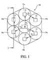
- FIG. 1illustrates a schematic top view of a multiple-chamber atomic layer doping apparatus according to the present invention.
- FIG. 2is a partial cross-sectional view of the atomic layer doping apparatus of FIG. 1, taken along line 2 - 2 ′ and depicting two adjacent doping regions according to a first embodiment of the present invention and depicting one wafer transfer sequence.
- FIG. 3is a partial cross-sectional view of the atomic layer doping apparatus of FIG. 1, taken along line 2 - 2 ′ and depicting two adjacent doping regions according to a second embodiment of the present invention.
- FIG. 4is a partial cross-sectional view of the atomic layer doping apparatus of FIG. 2, depicting a physical barrier between two adjacent doping chambers.
- FIG. 5is a schematic top view of a multiple-chamber atomic layer doping apparatus according to the present invention and depicting a second wafer transfer sequence.
- substrateused in the following description may include any semiconductor-based structure. Structure must be understood to include silicon, silicon-on insulator (SOI), silicon-on sapphire (SOS), doped and undoped semiconductors, epitaxial layers of silicon supported by a base semiconductor foundation, and other semiconductor structures.
- SOIsilicon-on insulator
- SOSsilicon-on sapphire
- the semiconductorneed not be silicon-based.
- the semiconductorcould be silicon-germanium, germanium, or gallium arsenide.
- previous process stepsmay have been utilized to form regions or junctions in or on the base semiconductor or foundation.
- dopantis intended to include not only elemental dopant atoms, but dopant atoms with other trace elements or in various combinations with other elements as known in the semiconductor art, as long as such combinations retain the physical and chemical properties of the dopant atoms.
- p-type dopantused in the following description may include any p-type impurity ions, such as zinc (Zn), magnesium (Mg), beryllium (Be), boron (B), gallium (Ga) or indium (In), among others.
- n-type dopantmay include any n-type impurity ions, such as silicon (Si), sulfur (S), tin (Sn), phosphorus (P), arsenic (As) or antimony (Sb), among others.
- the present inventionprovides an atomic layer doping method and apparatus.
- the apparatusis provided with multiple doping regions in which individual monolayer dopant species are first deposited on a substrate and then dopant atoms corresponding to each of the monolayer species are diffused into respective substrates.
- Each doping regionis chemically separated from the adjacent doping regions.
- a robotis programmed to follow pre-defined transfer sequences for moving wafers into and out of the respective adjacent doping regions. According to the number of doping regions provided, a multitude of substrates could be simultaneously processed and run through the cycle of different doping regions until a desired doping concentration of a wafer surface is completed.
- the present inventionprovides a simple and novel multi-chamber system for atomic layer doping processing.
- the present inventionwill be described below with reference to the atomic layer deposition of a dopant species Ax and the subsequent diffusion of its dopant atoms into a wafer, it must be understood that the present invention has equal applicability for the formation of any doped material capable of being formed by atomic layer doping techniques using any number of species, where each dopant species is deposited in a reaction chamber dedicated thereto.
- FIG. 1A schematic top view of a multiple-chamber atomic layer doping apparatus 100 of the present invention is shown in FIG. 1 .
- doping regions 50 a, 50 b, 52 a, 52 b, 54 a, and 54 bare alternately positioned around a loading mechanism 60 , for example a robot. These doping regions may be any regions for the atomic layer doping treatment of substrates.
- the doping regionsmay be formed as cylindrical reactor chambers, 50 a, 50 b, 52 a, 52 b, 54 a, and 54 b, in which adjacent chambers are chemically isolated from one another.
- the reactor chambersare arranged in pairs 50 a, 50 b; 52 a, 52 b; 54 a, 54 b.
- One such pair, 50 a, 50 bis shown in FIG. 2 . While one of the reactor chambers of a pair, for example 50 a, deposits one monolayer of the dopant species Ax, the other reactor chamber of the pair, for example 50 b, facilitates subsequent diffusion of the dopant atoms of species Ax into the wafer to complete the doping process.
- the adjacent reactor chamber pairsare chemically isolated from one another, for example by a gas curtain, which keeps the monolayer of dopant species Ax in a respective region, for example 50 a, and which allows wafers treated in one reaction chamber, for example 50 a, to be easily transported by the robot 60 to the other reaction chamber 50 b, and vice versa.
- the robotcan also move wafers between chambers 52 a or 52 b, and 54 a and 54 b.
- the paired reaction chambersshow a wall through which the wafers may pass, with the gas curtain acting in effect as a chemical barrier preventing the gas mixture within one chamber, for example 50 a, from entering the paired adjacent chamber, for example 50 b.
- the robotcan simply move wafers back and forth between the adjacent chambers, for example 50 a, 50 b, until the desired doping profile and/or concentration of the wafer is obtained.
- one or more additional chambersmay also be used for deposition of additional respective monolayers of dopant species, such as By, for example, with the additional chambers being chemically isolated from the chambers depositing the Ax monolayer dopant species in the same way the chambers for depositing the Ax species are chemically isolated.
- the loading assembly 60 of FIG. 1may include an elevator mechanism along with a wafer supply mechanism.
- the supply mechanismmay be further provided with clamps and pivot arms, so that a wafer 55 can be maneuvered by the robot and positioned according to the requirements of the atomic layer doping processing described in more detail below.
- a processing cycle for atomic layer doping on a wafer 55begins by selectively moving a first wafer 55 , from the loading assembly 60 to the chamber reactor 50 a, in the direction of arrow A 1 (FIG. 1 ).
- a second wafer 55 ′may be selectively moved by the loading assembly 60 to the chamber reactor 52 a, in the direction of arrow A 2 .
- a third wafer 55 ′′is also selectively moved by the loading assembly 60 to the chamber reactor 54 a, in the direction A 3 .
- each of chambers 50 a, 52 a, 54 aare ready for atomic layer deposition of a monolayer of a dopant species, for example Ax.
- FIG. 2illustrates a cross-sectional view of the apparatus 100 of FIG. 1, taken along line 2 - 2 ′ .
- FIG. 2shows only a cross-sectional view of adjacent reactor chambers 50 a and 50 b.
- the wafer 55is placed inside of the reactor chamber 50 a, which may be provided as a quartz or aluminum container 120 .
- the wafer 55is placed by the loading assembly 60 (FIG. 1) onto a suscepter 140 a (FIG. 2 ), which in turn is situated on a heater assembly 150 a.
- a dopant gas supply inlet 160 aMounted on the upper wall of the reactor chamber 50 a is a dopant gas supply inlet 160 a, which is further connected to a dopant gas supply source 162 a for a first dopant gas precursor Ax.
- An exhaust outlet 180 aconnected to an exhaust system 182 a, is situated on the opposite wall from the dopant gas supply inlet 160 a.
- the wafer 55is positioned on top of the suscepter 140 a (FIG. 2) by the loading assembly 60 , and then a first dopant gas precursor Ax is supplied into the reactor chamber 50 a through the dopant gas inlet 160 a.
- the first dopant gas precursor Axflows at a right angle onto the wafer 55 and reacts with its top substrate surface to form a first monolayer 210 a of the first dopant species Ax, by an atomic layer deposition mechanism.
- Preferred gas sources of dopantsare hydrated forms of dopant atoms such as arsine (AsH 3 ) and diborane (B 2 H 6 ).
- Gas sourcesoffer the advantage of precise control through pressure regulators and are favored for deposition on larger wafers.
- a liquid source of dopantsuch as chlorinated or brominated compounds of the desired element may be used.
- a liquid source of dopantsuch as chlorinated or brominated compounds of the desired element
- a boron liquid sourcefor example boron tribromide (BBr 3 ), or a phosphorous liquid source, for example phosphorous oxychloride (POCl 3 )
- an inert gassuch as nitrogen (N 2 )
- N 2nitrogen
- the inert gascarries the dopant vapors through a gas tube and creates a laminar flow of dopant atoms.
- reaction gasis also required to create the elemental dopant form in the tube.
- the reaction gasis oxygen, which creates the boron trioxide (B 2 O 3 ) which further deposits as a monolayer of boron trioxide on the surface of the wafer.
- the processing cycle for the wafer 55continues with the removal of the wafer 55 from the chamber reactor 50 a to the chamber reactor 50 b, in the direction of arrow B 1 , as also illustrated in FIG. 1 .
- the wafer 55is moved from the reactor chamber 50 a, through a gas curtain 300 (FIG. 2 ), to the reactor chamber 50 b, by the loading assembly 60 (FIG. 1) and in the direction of arrow B 1 of FIG. 2 . It is important to note that the gas curtain 300 provides chemical isolation between adjacent deposition regions.
- the loading assembly 60moves the wafer 55 through the gas curtain 300 , onto the suscepter 140 b situated in the reactor chamber 50 b, which, in contrast with the reactor chamber 50 a, contains no dopant source and no dopant species.
- a heater assembly 150 bis positioned under the suscepter 140 b to facilitate the diffusion of the dopant atoms from the newly deposited first monolayer 210 a of the first dopant species Ax into the wafer 55 .
- the heat from the heater assembly 150 bdrives the dopant atoms into the wafer 55 and further redistributes the dopant atoms from the first monolayer 210 a deeper into the wafer 55 to form a doped region 210 b of the first dopant species Ax.
- the surface concentration of dopant atomsis reduced and the distribution of dopant atoms continues, so that a precise and shallow doping distribution in the doped region 210 b of the wafer 55 is obtained. Accordingly, the depth of the doped region 210 b of the wafer 55 is controlled, first, by the repeatability of the atomic layer deposition for the monolayers of dopant species and, second, by the degree of diffusion of dopants form the monolayers of dopant species into the wafers.
- a plasma of a non-reactive gasmay be used to complete the diffusion of the dopant atoms into the doped region 210 b of the wafer 55 .
- a supply inlet 160 b(FIG. 2 ), which is further connected to a non-reactive gas supply source 162 b, for the plasma of the non-reactive gas, is mounted on the upper wall of the reactor chamber 50 b.
- An exhaust inlet 180 b, connected to an exhaust system 182 b,is further situated on the opposite wall to the non-reactive gas supply inlet 160 b.
- the non-reactive gas Byis supplied into the reactor chamber 50 b through the non-reactive gas inlet 160 b, the non-reactive gas By flowing at a right angle onto the deposited first monolayer 210 a of the first dopant species Ax. This way, particles of the non-reactive gas By “knock” the dopant atoms from the first monolayer 210 a of the first doping species Ax into the wafer 55 to form the doped region 210 b of the wafer 55 .
- the processcontinues with the removal of the wafer 55 from the reactor chamber 50 b, through the gas curtain 300 , and into the reactor chamber 50 a to continue the doping process. This process is repeated cycle after cycle, with the wafer 55 traveling back and forth between the reactor chamber 50 a, and the reactor chamber 50 b, to acquire the desired doping profile of the region 210 b.
- an anneal step in the atomic layer doping processis required, to restore any crystal damage and to electrically activate the dopant atoms.
- annealingcan be achieved by a thermal heating step.
- the anneal temperaturemust be preferably below the diffusion temperature to prevent lateral diffusion of the dopants.
- the anneal stepcould take place in the reactor chamber 50 b, for example, by controlling the heat from the heater assembly 150 b.
- the anneal stepmay take place into an adjacent reactor chamber, for example reactor chamber 52 a, depending on the processing requirements and the desired number of wafers to be processed.
- the present inventionhas the major advantage of allowing different processing conditions, for example, deposition or diffusion temperatures, in different reactor chambers. This is important since the chemisorption and reactivity requirements of the ALD process have specific temperature requirements, in accordance with the nature of the precursor gas. Accordingly, the apparatus of the present invention allows, for example, reactor chamber 50 a to be set to a different temperature than that of the reactor chamber 50 b. Further, each reactor chamber may be optimized either for improved chemisorption, reactivity or dopant conditions.
- the configuration of the atomic layer doping apparatus illustrated abovealso improves the overall yield and productivity of the doping process, since each chamber could run a separate substrate, and therefore, a plurality of substrates could be run simultaneously at a given time.
- each reactor chamberaccommodates only one dopant species, cross-contamination from one wafer to another is greatly reduced.
- the production timecan be decreased since the configuration of the apparatus of the present invention saves a great amount of purging and reactor clearing time.
- first and second reactor chambers 50 a, 50 bcould also process another first substrate 55 , in a direction opposite to that of processing the other first substrate. For example, if one first substrate 55 travels in the direction of arrow B 1 (FIG. 2) the other first substrate 55 could travel in the opposite direction of arrow B 1 , that is from the second reactor chamber 50 b to the first reactor chamber 50 a.
- the wafer 55is then moved back by the assembly system 60 to the reactor chamber 50 a, where a second monolayer of the first dopant species Ax is next deposited over the first monolayer of the first dopant species Ax.
- the wafer 55is further moved to the reactor chamber 50 b for the subsequent diffusion of the dopant atoms from the second monolayer of the first dopant species Ax.
- the cyclecontinues until a desired doping concentration on the surface of the wafer 55 is achieved, and, thus, the wafer 55 travels back and forth between reactor chambers 50 a and 50 b.
- the same cycle processapplies to the other two wafers 55 ′ , 55 ′′ that are processed simultaneously in their respective reactor chambers.
- the gas curtain 300provides chemical isolation to all adjacent deposition regions.
- the gas curtain 300is provided between the two adjacent reactor chambers 50 a and 50 b so that an inert gas 360 , such as nitrogen, argon, or helium, for example, flows through an inlet 260 connected to an inert gas supply source 362 to form the gas curtain 300 , which keeps the first dopant gas Ax and the non-reactive gas By from flowing into adjacent reaction chambers.
- An exhaust outlet 382(FIG.
- FIG. 3illustrates a cross-sectional view of the apparatus 100 of FIG. 2, with same adjacent reactor chambers 50 a and 50 b, but in which the inert gas 360 shares the exhaust outlets 180 a and 180 b with the two doping gases Ax and By, respectively.
- the atomic layer doping apparatus 100may be designed so that the inert gas 360 of the gas curtain 300 could be exhausted through either one or both of the two exhaust outlets 180 a and 180 b, instead of being exhausted through its own exhaust outlet 382 , as illustrated in FIG. 2 .
- FIG. 4shows another alternate embodiment of the apparatus in which the gas curtain 300 separating adjacent chambers in FIGS. 2-3 is replaced by a physical boundary, such as a wall 170 having a closeable opening 172 .
- a door 174(FIG. 4) can be used to open and close the opening 172 between the adjacent paired chambers 50 a, 50 b. This way, the wafer 55 can be passed between the adjacent chambers 50 a, 50 b through the open opening 172 by the robot 60 , with the door 174 closing the opening 172 during atomic layer doping processing.
- two speciesfor example, Ax and a second dopant species Cz
- Czthe non-reactive gas
- Other combinationsare also possible.
- the inventionhas been described with the wafer 55 traveling back and forth from the reactor chamber 50 a to the reactor chamber 50 b with reference to FIG. 2, it must be understood that, when more than two reactor chambers are used for doping with more than two monolayer species Ax, Cz, the wafer 55 will be transported by the loading assembly 60 among all the reaction chambers in a sequence required to produce a desired doping profile.
- a processing cycle for atomic layer deposition on a plurality of wafers 55begins by selectively moving each wafer 55 , from the loading assembly 60 to the chamber reactor 50 a, in the direction of arrow A 1 (FIG. 5 ), and then further to the reactor chamber 50 b, 52 a, 52 b, 54 a, and 54 b.
- One reaction chamber, for example 50 acan serve as the initial chamber and another, for example 54 b, as the final chamber.
- Each wafer 55is simultaneously processed in a respective chamber and is moved sequentially through the chambers by the loading assembly 60 , with the cycle continuing with wafers 55 traveling in one direction to all the remaining reactors chambers.
Landscapes
- Engineering & Computer Science (AREA)
- Physics & Mathematics (AREA)
- Condensed Matter Physics & Semiconductors (AREA)
- General Physics & Mathematics (AREA)
- Manufacturing & Machinery (AREA)
- Computer Hardware Design (AREA)
- Microelectronics & Electronic Packaging (AREA)
- Power Engineering (AREA)
- Crystals, And After-Treatments Of Crystals (AREA)
- Physical Deposition Of Substances That Are Components Of Semiconductor Devices (AREA)
- Junction Field-Effect Transistors (AREA)
Abstract
Description
Claims (11)
Priority Applications (11)
| Application Number | Priority Date | Filing Date | Title |
|---|---|---|---|
| US09/653,553US6541353B1 (en) | 2000-08-31 | 2000-08-31 | Atomic layer doping apparatus and method |
| JP2002541151AJP2004513525A (en) | 2000-08-31 | 2001-08-22 | Atomic layer doping apparatus and method |
| AT01985952TATE282101T1 (en) | 2000-08-31 | 2001-08-22 | DEVICE AND METHOD FOR DOPPING ATOMIC LAYERS |
| AU2002236430AAU2002236430A1 (en) | 2000-08-31 | 2001-08-22 | Atomic layer doping apparatus and method |
| EP01985952AEP1335998B1 (en) | 2000-08-31 | 2001-08-22 | Atomic layer doping apparatus and method |
| DE60107111TDE60107111T2 (en) | 2000-08-31 | 2001-08-22 | DEVICE AND METHOD FOR DOPING ATOMIC LAYERS |
| KR1020037003141AKR100564977B1 (en) | 2000-08-31 | 2001-08-22 | Atomic Layer Doping Apparatus and Method |
| PCT/US2001/026079WO2002038841A2 (en) | 2000-08-31 | 2001-08-22 | Atomic layer doping apparatus and method |
| CNB018166695ACN1267589C (en) | 2000-08-31 | 2001-08-22 | Atomic layer doping apparatus and method |
| US09/982,954US20020046705A1 (en) | 2000-08-31 | 2001-10-22 | Atomic layer doping apparatus and method |
| US10/301,573US6746934B2 (en) | 2000-08-31 | 2002-11-22 | Atomic layer doping apparatus and method |
Applications Claiming Priority (1)
| Application Number | Priority Date | Filing Date | Title |
|---|---|---|---|
| US09/653,553US6541353B1 (en) | 2000-08-31 | 2000-08-31 | Atomic layer doping apparatus and method |
Related Child Applications (2)
| Application Number | Title | Priority Date | Filing Date |
|---|---|---|---|
| US09/982,954DivisionUS20020046705A1 (en) | 2000-08-31 | 2001-10-22 | Atomic layer doping apparatus and method |
| US10/301,573ContinuationUS6746934B2 (en) | 2000-08-31 | 2002-11-22 | Atomic layer doping apparatus and method |
Publications (1)
| Publication Number | Publication Date |
|---|---|
| US6541353B1true US6541353B1 (en) | 2003-04-01 |
Family
ID=24621343
Family Applications (3)
| Application Number | Title | Priority Date | Filing Date |
|---|---|---|---|
| US09/653,553Expired - LifetimeUS6541353B1 (en) | 2000-08-31 | 2000-08-31 | Atomic layer doping apparatus and method |
| US09/982,954AbandonedUS20020046705A1 (en) | 2000-08-31 | 2001-10-22 | Atomic layer doping apparatus and method |
| US10/301,573Expired - LifetimeUS6746934B2 (en) | 2000-08-31 | 2002-11-22 | Atomic layer doping apparatus and method |
Family Applications After (2)
| Application Number | Title | Priority Date | Filing Date |
|---|---|---|---|
| US09/982,954AbandonedUS20020046705A1 (en) | 2000-08-31 | 2001-10-22 | Atomic layer doping apparatus and method |
| US10/301,573Expired - LifetimeUS6746934B2 (en) | 2000-08-31 | 2002-11-22 | Atomic layer doping apparatus and method |
Country Status (9)
| Country | Link |
|---|---|
| US (3) | US6541353B1 (en) |
| EP (1) | EP1335998B1 (en) |
| JP (1) | JP2004513525A (en) |
| KR (1) | KR100564977B1 (en) |
| CN (1) | CN1267589C (en) |
| AT (1) | ATE282101T1 (en) |
| AU (1) | AU2002236430A1 (en) |
| DE (1) | DE60107111T2 (en) |
| WO (1) | WO2002038841A2 (en) |
Cited By (65)
| Publication number | Priority date | Publication date | Assignee | Title |
|---|---|---|---|---|
| US20020100418A1 (en)* | 2000-05-12 | 2002-08-01 | Gurtej Sandhu | Versatile atomic layer deposition apparatus |
| US20020122885A1 (en)* | 2001-03-01 | 2002-09-05 | Micron Technology, Inc. | Methods, systems, and apparatus for uniform chemical-vapor depositions |
| US20030159780A1 (en)* | 2002-02-22 | 2003-08-28 | Carpenter Craig M. | Interfacial structure for semiconductor substrate processing chambers and substrate transfer chambers and for semiconductor substrate processing chambers and accessory attachments, and semiconductor substrate processor |
| US20030203109A1 (en)* | 2002-04-24 | 2003-10-30 | Dando Ross S. | Chemical vapor deposition methods |
| US20030200926A1 (en)* | 2002-04-24 | 2003-10-30 | Dando Ross S. | Chemical vapor deposition apparatus |
| US20030226500A1 (en)* | 2002-06-05 | 2003-12-11 | Derderian Garo J. | Atomic layer deposition apparatus and methods |
| US20040026374A1 (en)* | 2002-08-06 | 2004-02-12 | Tue Nguyen | Assembly line processing method |
| US20040043541A1 (en)* | 2002-08-29 | 2004-03-04 | Ahn Kie Y. | Atomic layer deposited lanthanide doped TiOx dielectric films |
| US20040065258A1 (en)* | 2002-10-08 | 2004-04-08 | Sandhu Gurtej S. | Atomic layer deposition methods and atomic layer deposition tools |
| US20040110348A1 (en)* | 2002-12-04 | 2004-06-10 | Micron Technology, Inc. | Atomic layer deposited Zr-Sn-Ti-O films using TiI4 |
| US20040110391A1 (en)* | 2002-12-04 | 2004-06-10 | Micron Technology, Inc. | Atomic layer deposited Zr-Sn-Ti-O films |
| US20040164365A1 (en)* | 2002-08-15 | 2004-08-26 | Micron Technology, Inc. | Lanthanide doped TiOx dielectric films |
| US20040175882A1 (en)* | 2003-03-04 | 2004-09-09 | Micron Technology, Inc. | Atomic layer deposited dielectric layers |
| US20040187784A1 (en)* | 2003-03-28 | 2004-09-30 | Fluens Corporation | Continuous flow deposition system |
| US20040233010A1 (en)* | 2003-05-22 | 2004-11-25 | Salman Akram | Atomic layer deposition (ALD) high permeability layered magnetic films to reduce noise in high speed interconnection |
| US20050020017A1 (en)* | 2003-06-24 | 2005-01-27 | Micron Technology, Inc. | Lanthanide oxide / hafnium oxide dielectric layers |
| US20050028734A1 (en)* | 2003-02-11 | 2005-02-10 | Carpenter Craig M. | Reactors with isolated gas connectors and methods for depositing materials onto micro-device workpieces |
| US20050064212A1 (en)* | 2001-02-23 | 2005-03-24 | Dunlap Paul N. | Bonded part and method for producing same |
| US20050061243A1 (en)* | 2003-09-18 | 2005-03-24 | Demetrius Sarigiannis | Systems and methods for depositing material onto microfeature workpieces in reaction chambers |
| US20050081786A1 (en)* | 2003-10-15 | 2005-04-21 | Kubista David J. | Systems for depositing material onto workpieces in reaction chambers and methods for removing byproducts from reaction chambers |
| US20050164466A1 (en)* | 2004-01-28 | 2005-07-28 | Zheng Lingyi A. | Methods for forming small-scale capacitor structures |
| US20060006548A1 (en)* | 2003-08-05 | 2006-01-12 | Micron Technology, Inc. | H2 plasma treatment |
| US20060040475A1 (en)* | 2004-08-18 | 2006-02-23 | Emerson David T | Multi-chamber MOCVD growth apparatus for high performance/high throughput |
| US7056806B2 (en) | 2003-09-17 | 2006-06-06 | Micron Technology, Inc. | Microfeature workpiece processing apparatus and methods for controlling deposition of materials on microfeature workpieces |
| US20060131702A1 (en)* | 1999-07-30 | 2006-06-22 | Micron Technology, Inc. | Novel transmission lines for CMOS integrated circuits |
| US20060177975A1 (en)* | 2005-02-10 | 2006-08-10 | Micron Technology, Inc. | Atomic layer deposition of CeO2/Al2O3 films as gate dielectrics |
| US20060237138A1 (en)* | 2005-04-26 | 2006-10-26 | Micron Technology, Inc. | Apparatuses and methods for supporting microelectronic devices during plasma-based fabrication processes |
| US20060246741A1 (en)* | 2002-07-30 | 2006-11-02 | Micron Technology, Inc. | ATOMIC LAYER DEPOSITED NANOLAMINATES OF HfO2/ZrO2 FILMS AS GATE DIELECTRICS |
| US7135369B2 (en) | 2003-03-31 | 2006-11-14 | Micron Technology, Inc. | Atomic layer deposited ZrAlxOy dielectric layers including Zr4AlO9 |
| US7160577B2 (en) | 2002-05-02 | 2007-01-09 | Micron Technology, Inc. | Methods for atomic-layer deposition of aluminum oxides in integrated circuits |
| US7235138B2 (en) | 2003-08-21 | 2007-06-26 | Micron Technology, Inc. | Microfeature workpiece processing apparatus and methods for batch deposition of materials on microfeature workpieces |
| US20070151842A1 (en)* | 2005-12-15 | 2007-07-05 | Fluens Corporation | Apparatus for reactive sputtering |
| US7258892B2 (en) | 2003-12-10 | 2007-08-21 | Micron Technology, Inc. | Methods and systems for controlling temperature during microfeature workpiece processing, e.g., CVD deposition |
| US7323231B2 (en) | 2003-10-09 | 2008-01-29 | Micron Technology, Inc. | Apparatus and methods for plasma vapor deposition processes |
| US7335396B2 (en) | 2003-04-24 | 2008-02-26 | Micron Technology, Inc. | Methods for controlling mass flow rates and pressures in passageways coupled to reaction chambers and systems for depositing material onto microfeature workpieces in reaction chambers |
| US7344755B2 (en) | 2003-08-21 | 2008-03-18 | Micron Technology, Inc. | Methods and apparatus for processing microfeature workpieces; methods for conditioning ALD reaction chambers |
| US20080110568A1 (en)* | 2006-11-10 | 2008-05-15 | Adp Engineering Co., Ltd. | Process chamber having gate slit opening and closing apparatus |
| US7387685B2 (en) | 2002-07-08 | 2008-06-17 | Micron Technology, Inc. | Apparatus and method for depositing materials onto microelectronic workpieces |
| US20080166861A1 (en)* | 2005-03-30 | 2008-07-10 | Matsushita Electric Industrial Co., Ltd. | Impurity introducing apparatus and impurity introducing method |
| US20080194072A1 (en)* | 2007-02-12 | 2008-08-14 | Chen-Hua Yu | Polysilicon gate formation by in-situ doping |
| US20080194087A1 (en)* | 2007-02-12 | 2008-08-14 | Chen-Hua Yu | Polysilicon gate formation by in-situ doping |
| US7422635B2 (en) | 2003-08-28 | 2008-09-09 | Micron Technology, Inc. | Methods and apparatus for processing microfeature workpieces, e.g., for depositing materials on microfeature workpieces |
| US7429515B2 (en) | 2001-12-20 | 2008-09-30 | Micron Technology, Inc. | Low-temperature grown high quality ultra-thin CoTiO3 gate dielectrics |
| US7481887B2 (en) | 2002-05-24 | 2009-01-27 | Micron Technology, Inc. | Apparatus for controlling gas pulsing in processes for depositing materials onto micro-device workpieces |
| US7544398B1 (en)* | 2005-04-26 | 2009-06-09 | The Regents Of The Univesity Of California | Controlled nano-doping of ultra thin films |
| US7554161B2 (en) | 2002-06-05 | 2009-06-30 | Micron Technology, Inc. | HfAlO3 films for gate dielectrics |
| US7560793B2 (en) | 2002-05-02 | 2009-07-14 | Micron Technology, Inc. | Atomic layer deposition and conversion |
| US7581511B2 (en) | 2003-10-10 | 2009-09-01 | Micron Technology, Inc. | Apparatus and methods for manufacturing microfeatures on workpieces using plasma vapor processes |
| US7584942B2 (en) | 2004-03-31 | 2009-09-08 | Micron Technology, Inc. | Ampoules for producing a reaction gas and systems for depositing materials onto microfeature workpieces in reaction chambers |
| US7588988B2 (en) | 2004-08-31 | 2009-09-15 | Micron Technology, Inc. | Method of forming apparatus having oxide films formed using atomic layer deposition |
| US7588804B2 (en) | 2002-08-15 | 2009-09-15 | Micron Technology, Inc. | Reactors with isolated gas connectors and methods for depositing materials onto micro-device workpieces |
| US7662729B2 (en) | 2005-04-28 | 2010-02-16 | Micron Technology, Inc. | Atomic layer deposition of a ruthenium layer to a lanthanide oxide dielectric layer |
| US20100068873A1 (en)* | 2008-09-16 | 2010-03-18 | Jing-Cheng Lin | Depletion-Free MOS using Atomic-Layer Doping |
| US7687409B2 (en) | 2005-03-29 | 2010-03-30 | Micron Technology, Inc. | Atomic layer deposited titanium silicon oxide films |
| US7699932B2 (en) | 2004-06-02 | 2010-04-20 | Micron Technology, Inc. | Reactors, systems and methods for depositing thin films onto microfeature workpieces |
| US7728626B2 (en) | 2002-07-08 | 2010-06-01 | Micron Technology, Inc. | Memory utilizing oxide nanolaminates |
| US20100221426A1 (en)* | 2009-03-02 | 2010-09-02 | Fluens Corporation | Web Substrate Deposition System |
| US20100316800A1 (en)* | 2002-04-16 | 2010-12-16 | Mei Chang | Multi-station deposition apparatus and method |
| US20110057289A1 (en)* | 2009-03-06 | 2011-03-10 | Texas Instruments Incorporated | Ultrashallow Emitter Formation Using ALD and High Temperature Short Time Annealing |
| US8133554B2 (en) | 2004-05-06 | 2012-03-13 | Micron Technology, Inc. | Methods for depositing material onto microfeature workpieces in reaction chambers and systems for depositing materials onto microfeature workpieces |
| US8501563B2 (en) | 2005-07-20 | 2013-08-06 | Micron Technology, Inc. | Devices with nanocrystals and methods of formation |
| US8518829B2 (en) | 2011-04-22 | 2013-08-27 | International Business Machines Corporation | Self-sealed fluidic channels for nanopore array |
| US8828138B2 (en) | 2010-05-17 | 2014-09-09 | International Business Machines Corporation | FET nanopore sensor |
| US10808315B2 (en)* | 2015-10-05 | 2020-10-20 | Jusung Engineering Co., Ltd. | Substrate processing apparatus having exhaust gas decomposer, and exhaust gas processing method therefor |
| US12421604B2 (en) | 2021-08-20 | 2025-09-23 | Tokyo Electron Limited | Ultra-shallow dopant and ohmic contact regions by solid state diffusion |
Families Citing this family (41)
| Publication number | Priority date | Publication date | Assignee | Title |
|---|---|---|---|---|
| DE10101014A1 (en)* | 2001-01-05 | 2002-07-11 | Zeiss Carl | Coating of optical elements, especially for use with ultraviolet light |
| US6893984B2 (en)* | 2002-02-20 | 2005-05-17 | Micron Technology Inc. | Evaporated LaA1O3 films for gate dielectrics |
| DE10208450B4 (en)* | 2002-02-27 | 2004-09-16 | Infineon Technologies Ag | Process for the deposition of thin layers by means of ALD / CVD processes in connection with fast thermal processes |
| US6962644B2 (en)* | 2002-03-18 | 2005-11-08 | Applied Materials, Inc. | Tandem etch chamber plasma processing system |
| US7887711B2 (en)* | 2002-06-13 | 2011-02-15 | International Business Machines Corporation | Method for etching chemically inert metal oxides |
| US20040058293A1 (en)* | 2002-08-06 | 2004-03-25 | Tue Nguyen | Assembly line processing system |
| US6884739B2 (en)* | 2002-08-15 | 2005-04-26 | Micron Technology Inc. | Lanthanide doped TiOx dielectric films by plasma oxidation |
| US7199023B2 (en) | 2002-08-28 | 2007-04-03 | Micron Technology, Inc. | Atomic layer deposited HfSiON dielectric films wherein each precursor is independendently pulsed |
| DE10339991A1 (en)* | 2003-08-29 | 2005-03-31 | Advanced Micro Devices, Inc., Sunnyvale | Improved technique for adjusting a penetration depth during the implantation of ions into a semiconductor region |
| EP1776321A1 (en)* | 2004-06-24 | 2007-04-25 | Beneq Oy | Method for doping material and doped material |
| US7601649B2 (en) | 2004-08-02 | 2009-10-13 | Micron Technology, Inc. | Zirconium-doped tantalum oxide films |
| US7081421B2 (en) | 2004-08-26 | 2006-07-25 | Micron Technology, Inc. | Lanthanide oxide dielectric layer |
| US7494939B2 (en) | 2004-08-31 | 2009-02-24 | Micron Technology, Inc. | Methods for forming a lanthanum-metal oxide dielectric layer |
| US20060137609A1 (en)* | 2004-09-13 | 2006-06-29 | Puchacz Jerzy P | Multi-single wafer processing apparatus |
| US20060125030A1 (en)* | 2004-12-13 | 2006-06-15 | Micron Technology, Inc. | Hybrid ALD-CVD of PrxOy/ZrO2 films as gate dielectrics |
| US7235501B2 (en) | 2004-12-13 | 2007-06-26 | Micron Technology, Inc. | Lanthanum hafnium oxide dielectrics |
| KR100579860B1 (en)* | 2004-12-23 | 2006-05-12 | 동부일렉트로닉스 주식회사 | Method for forming P-type polysilicon film of semiconductor device using atomic layer deposition method (ALD) and group III heavy metal |
| US7560395B2 (en) | 2005-01-05 | 2009-07-14 | Micron Technology, Inc. | Atomic layer deposited hafnium tantalum oxide dielectrics |
| US7508648B2 (en)* | 2005-02-08 | 2009-03-24 | Micron Technology, Inc. | Atomic layer deposition of Dy doped HfO2 films as gate dielectrics |
| US7399666B2 (en)* | 2005-02-15 | 2008-07-15 | Micron Technology, Inc. | Atomic layer deposition of Zr3N4/ZrO2 films as gate dielectrics |
| KR100760428B1 (en)* | 2005-05-13 | 2007-09-20 | 오재응 | Vapor deposition reactor |
| US7393736B2 (en)* | 2005-08-29 | 2008-07-01 | Micron Technology, Inc. | Atomic layer deposition of Zrx Hfy Sn1-x-y O2 films as high k gate dielectrics |
| US7410910B2 (en) | 2005-08-31 | 2008-08-12 | Micron Technology, Inc. | Lanthanum aluminum oxynitride dielectric films |
| US20070065576A1 (en)* | 2005-09-09 | 2007-03-22 | Vikram Singh | Technique for atomic layer deposition |
| US20070087581A1 (en)* | 2005-09-09 | 2007-04-19 | Varian Semiconductor Equipment Associates, Inc. | Technique for atomic layer deposition |
| CN1937175B (en)* | 2005-09-20 | 2012-10-03 | 中芯国际集成电路制造(上海)有限公司 | Method for depositing material atomic layer for semiconductor device by using atmosphere |
| US7709402B2 (en) | 2006-02-16 | 2010-05-04 | Micron Technology, Inc. | Conductive layers for hafnium silicon oxynitride films |
| US20070212859A1 (en) | 2006-03-08 | 2007-09-13 | Paul Carey | Method of thermal processing structures formed on a substrate |
| US7605030B2 (en)* | 2006-08-31 | 2009-10-20 | Micron Technology, Inc. | Hafnium tantalum oxynitride high-k dielectric and metal gates |
| US7759237B2 (en) | 2007-06-28 | 2010-07-20 | Micron Technology, Inc. | Method of forming lutetium and lanthanum dielectric structures |
| US20090081356A1 (en)* | 2007-09-26 | 2009-03-26 | Fedorovskaya Elena A | Process for forming thin film encapsulation layers |
| TWI471961B (en)* | 2007-10-26 | 2015-02-01 | Sosul Co Ltd | Baffle, substrate supporting apparatus and plasma processing apparatus and plasma processing method |
| US8361895B2 (en)* | 2008-09-16 | 2013-01-29 | Taiwan Semiconductor Manufacturing Company, Ltd. | Ultra-shallow junctions using atomic-layer doping |
| JP2010153278A (en)* | 2008-12-26 | 2010-07-08 | Hitachi High-Technologies Corp | Charged particle beam processing device |
| JP5295095B2 (en)* | 2008-12-29 | 2013-09-18 | ケー.シー.テック カンパニー リミテッド | Atomic layer deposition equipment |
| FI122940B (en)* | 2009-02-09 | 2012-09-14 | Beneq Oy | reaction chamber |
| US20140065799A1 (en)* | 2012-09-03 | 2014-03-06 | Intermolecular, Inc. | Methods and Systems for Low Resistance Contact Formation |
| US20140199854A1 (en)* | 2013-01-16 | 2014-07-17 | United Microelectronics Corp. | Method of forming film on different surfaces |
| US8940646B1 (en)* | 2013-07-12 | 2015-01-27 | Lam Research Corporation | Sequential precursor dosing in an ALD multi-station/batch reactor |
| US20160002784A1 (en) | 2014-07-07 | 2016-01-07 | Varian Semiconductor Equipment Associates, Inc. | Method and apparatus for depositing a monolayer on a three dimensional structure |
| KR102622159B1 (en)* | 2021-07-14 | 2024-01-09 | 한국생산기술연구원 | atomic layer deposition chamber |
Citations (14)
| Publication number | Priority date | Publication date | Assignee | Title |
|---|---|---|---|---|
| US4533410A (en) | 1982-10-19 | 1985-08-06 | Matsushita Electric Industrial Co., Ltd. | Process of vapor phase epitaxy of compound semiconductors |
| US4951601A (en)* | 1986-12-19 | 1990-08-28 | Applied Materials, Inc. | Multi-chamber integrated process system |
| US5013683A (en)* | 1989-01-23 | 1991-05-07 | The Regents Of The University Of California | Method for growing tilted superlattices |
| US5281274A (en) | 1990-06-22 | 1994-01-25 | The United States Of America As Represented By The Secretary Of The Navy | Atomic layer epitaxy (ALE) apparatus for growing thin films of elemental semiconductors |
| US5298452A (en)* | 1986-09-12 | 1994-03-29 | International Business Machines Corporation | Method and apparatus for low temperature, low pressure chemical vapor deposition of epitaxial silicon layers |
| US5310698A (en) | 1990-12-21 | 1994-05-10 | Siemens Aktiengesellschaft | Process for producing an arsenic-doped smooth polycrystalline silicon layer for very large scale integrated circuits |
| US5527733A (en) | 1989-07-27 | 1996-06-18 | Seiko Instruments Inc. | Impurity doping method with adsorbed diffusion source |
| US5793109A (en) | 1995-08-25 | 1998-08-11 | Advantest Corp. | Structure of ohmic electrode for semiconductor by atomic layer doping |
| US5916365A (en)* | 1996-08-16 | 1999-06-29 | Sherman; Arthur | Sequential chemical vapor deposition |
| US6048781A (en)* | 1996-05-31 | 2000-04-11 | Micron Technology, Inc. | Semiconductor processing method for providing large grain polysilicon films |
| US6056849A (en)* | 1997-01-07 | 2000-05-02 | Straemke; Siegfried | Apparatus for the surface treatment of workpieces by means of a plasma |
| US6207005B1 (en)* | 1997-07-29 | 2001-03-27 | Silicon Genesis Corporation | Cluster tool apparatus using plasma immersion ion implantation |
| US6319553B1 (en)* | 1998-10-08 | 2001-11-20 | Novellus Systems, Inc. | Isolation of incompatible processes in a multi-station processing chamber |
| US20020108714A1 (en)* | 1997-03-03 | 2002-08-15 | Kenneth Doering | Processing chamber for atomic layer deposition processes |
Family Cites Families (23)
| Publication number | Priority date | Publication date | Assignee | Title |
|---|---|---|---|---|
| US4089735A (en)* | 1968-06-05 | 1978-05-16 | Siemens Aktiengesellschaft | Method for epitactic precipitation of crystalline material from a gaseous phase, particularly for semiconductors |
| DE1758751A1 (en)* | 1968-08-01 | 1971-02-25 | Telefunken Patent | Oven for the diffusion of interference points in semiconductor bodies |
| US3602192A (en)* | 1969-05-19 | 1971-08-31 | Ibm | Semiconductor wafer processing |
| US3618919A (en)* | 1969-11-03 | 1971-11-09 | Btu Eng Corp | Adjustable heat and gas barrier |
| US3811826A (en)* | 1972-11-03 | 1974-05-21 | Sowell J | Diffusion furnace process tube |
| US4593644A (en)* | 1983-10-26 | 1986-06-10 | Rca Corporation | Continuous in-line deposition system |
| US4576830A (en)* | 1984-11-05 | 1986-03-18 | Chronar Corp. | Deposition of materials |
| US4786616A (en)* | 1987-06-12 | 1988-11-22 | American Telephone And Telegraph Company | Method for heteroepitaxial growth using multiple MBE chambers |
| JPH01278714A (en)* | 1988-04-30 | 1989-11-09 | Sharp Corp | Atomic layer planar doping method |
| JPH0824191B2 (en)* | 1989-03-17 | 1996-03-06 | 富士通株式会社 | Thin film transistor |
| US5071670A (en)* | 1990-06-11 | 1991-12-10 | Kelly Michael A | Method for chemical vapor deposition under a single reactor vessel divided into separate reaction chambers each with its own depositing and exhausting means |
| JPH0812847B2 (en)* | 1991-04-22 | 1996-02-07 | 株式会社半導体プロセス研究所 | Semiconductor manufacturing apparatus and semiconductor device manufacturing method |
| JP3049894B2 (en)* | 1991-11-27 | 2000-06-05 | 日本ゼオン株式会社 | Acrylic ester copolymer plastisol composition |
| US5667592A (en)* | 1996-04-16 | 1997-09-16 | Gasonics International | Process chamber sleeve with ring seals for isolating individual process modules in a common cluster |
| US5747113A (en)* | 1996-07-29 | 1998-05-05 | Tsai; Charles Su-Chang | Method of chemical vapor deposition for producing layer variation by planetary susceptor rotation |
| JP3239779B2 (en)* | 1996-10-29 | 2001-12-17 | 日新電機株式会社 | Substrate processing apparatus and substrate processing method |
| US6305314B1 (en)* | 1999-03-11 | 2001-10-23 | Genvs, Inc. | Apparatus and concept for minimizing parasitic chemical vapor deposition during atomic layer deposition |
| US6503330B1 (en)* | 1999-12-22 | 2003-01-07 | Genus, Inc. | Apparatus and method to achieve continuous interface and ultrathin film during atomic layer deposition |
| US6576062B2 (en)* | 2000-01-06 | 2003-06-10 | Tokyo Electron Limited | Film forming apparatus and film forming method |
| US6527866B1 (en)* | 2000-02-09 | 2003-03-04 | Conductus, Inc. | Apparatus and method for deposition of thin films |
| US20020195056A1 (en)* | 2000-05-12 | 2002-12-26 | Gurtej Sandhu | Versatile atomic layer deposition apparatus |
| US6482733B2 (en)* | 2000-05-15 | 2002-11-19 | Asm Microchemistry Oy | Protective layers prior to alternating layer deposition |
| US20030054133A1 (en)* | 2000-08-07 | 2003-03-20 | Wadley Hadyn N.G. | Apparatus and method for intra-layer modulation of the material deposition and assist beam and the multilayer structure produced therefrom |
- 2000
- 2000-08-31USUS09/653,553patent/US6541353B1/ennot_activeExpired - Lifetime
- 2001
- 2001-08-22EPEP01985952Apatent/EP1335998B1/ennot_activeExpired - Lifetime
- 2001-08-22KRKR1020037003141Apatent/KR100564977B1/ennot_activeExpired - Fee Related
- 2001-08-22AUAU2002236430Apatent/AU2002236430A1/ennot_activeAbandoned
- 2001-08-22JPJP2002541151Apatent/JP2004513525A/enactivePending
- 2001-08-22DEDE60107111Tpatent/DE60107111T2/ennot_activeExpired - Lifetime
- 2001-08-22ATAT01985952Tpatent/ATE282101T1/ennot_activeIP Right Cessation
- 2001-08-22WOPCT/US2001/026079patent/WO2002038841A2/enactiveIP Right Grant
- 2001-08-22CNCNB018166695Apatent/CN1267589C/ennot_activeExpired - Fee Related
- 2001-10-22USUS09/982,954patent/US20020046705A1/ennot_activeAbandoned
- 2002
- 2002-11-22USUS10/301,573patent/US6746934B2/ennot_activeExpired - Lifetime
Patent Citations (14)
| Publication number | Priority date | Publication date | Assignee | Title |
|---|---|---|---|---|
| US4533410A (en) | 1982-10-19 | 1985-08-06 | Matsushita Electric Industrial Co., Ltd. | Process of vapor phase epitaxy of compound semiconductors |
| US5298452A (en)* | 1986-09-12 | 1994-03-29 | International Business Machines Corporation | Method and apparatus for low temperature, low pressure chemical vapor deposition of epitaxial silicon layers |
| US4951601A (en)* | 1986-12-19 | 1990-08-28 | Applied Materials, Inc. | Multi-chamber integrated process system |
| US5013683A (en)* | 1989-01-23 | 1991-05-07 | The Regents Of The University Of California | Method for growing tilted superlattices |
| US5527733A (en) | 1989-07-27 | 1996-06-18 | Seiko Instruments Inc. | Impurity doping method with adsorbed diffusion source |
| US5281274A (en) | 1990-06-22 | 1994-01-25 | The United States Of America As Represented By The Secretary Of The Navy | Atomic layer epitaxy (ALE) apparatus for growing thin films of elemental semiconductors |
| US5310698A (en) | 1990-12-21 | 1994-05-10 | Siemens Aktiengesellschaft | Process for producing an arsenic-doped smooth polycrystalline silicon layer for very large scale integrated circuits |
| US5793109A (en) | 1995-08-25 | 1998-08-11 | Advantest Corp. | Structure of ohmic electrode for semiconductor by atomic layer doping |
| US6048781A (en)* | 1996-05-31 | 2000-04-11 | Micron Technology, Inc. | Semiconductor processing method for providing large grain polysilicon films |
| US5916365A (en)* | 1996-08-16 | 1999-06-29 | Sherman; Arthur | Sequential chemical vapor deposition |
| US6056849A (en)* | 1997-01-07 | 2000-05-02 | Straemke; Siegfried | Apparatus for the surface treatment of workpieces by means of a plasma |
| US20020108714A1 (en)* | 1997-03-03 | 2002-08-15 | Kenneth Doering | Processing chamber for atomic layer deposition processes |
| US6207005B1 (en)* | 1997-07-29 | 2001-03-27 | Silicon Genesis Corporation | Cluster tool apparatus using plasma immersion ion implantation |
| US6319553B1 (en)* | 1998-10-08 | 2001-11-20 | Novellus Systems, Inc. | Isolation of incompatible processes in a multi-station processing chamber |
Cited By (147)
| Publication number | Priority date | Publication date | Assignee | Title |
|---|---|---|---|---|
| US20060131702A1 (en)* | 1999-07-30 | 2006-06-22 | Micron Technology, Inc. | Novel transmission lines for CMOS integrated circuits |
| US7869242B2 (en) | 1999-07-30 | 2011-01-11 | Micron Technology, Inc. | Transmission lines for CMOS integrated circuits |
| US7554829B2 (en) | 1999-07-30 | 2009-06-30 | Micron Technology, Inc. | Transmission lines for CMOS integrated circuits |
| US20020195056A1 (en)* | 2000-05-12 | 2002-12-26 | Gurtej Sandhu | Versatile atomic layer deposition apparatus |
| US20020100418A1 (en)* | 2000-05-12 | 2002-08-01 | Gurtej Sandhu | Versatile atomic layer deposition apparatus |
| US20050064212A1 (en)* | 2001-02-23 | 2005-03-24 | Dunlap Paul N. | Bonded part and method for producing same |
| US6852167B2 (en) | 2001-03-01 | 2005-02-08 | Micron Technology, Inc. | Methods, systems, and apparatus for uniform chemical-vapor depositions |
| US20020122885A1 (en)* | 2001-03-01 | 2002-09-05 | Micron Technology, Inc. | Methods, systems, and apparatus for uniform chemical-vapor depositions |
| US7410668B2 (en) | 2001-03-01 | 2008-08-12 | Micron Technology, Inc. | Methods, systems, and apparatus for uniform chemical-vapor depositions |
| US20110014767A1 (en)* | 2001-12-20 | 2011-01-20 | Ahn Kie Y | LOW-TEMPERATURE GROWN HIGH QUALITY ULTRA-THIN CoTiO3 GATE DIELECTRICS |
| US20080283940A1 (en)* | 2001-12-20 | 2008-11-20 | Micron Technology, Inc. | LOW-TEMPERATURE GROWN HIGH QUALITY ULTRA-THIN CoTiO3 GATE DIELECTRICS |
| US7429515B2 (en) | 2001-12-20 | 2008-09-30 | Micron Technology, Inc. | Low-temperature grown high quality ultra-thin CoTiO3 gate dielectrics |
| US8178413B2 (en) | 2001-12-20 | 2012-05-15 | Micron Technology, Inc. | Low-temperature grown high quality ultra-thin CoTiO3 gate dielectrics |
| US7804144B2 (en) | 2001-12-20 | 2010-09-28 | Micron Technology, Inc. | Low-temperature grown high quality ultra-thin CoTiO3 gate dielectrics |
| US20040144315A1 (en)* | 2002-02-22 | 2004-07-29 | Carpenter Craig M | Semiconductor substrate processing chamber and accessory attachment interfacial structure |
| US20060027326A1 (en)* | 2002-02-22 | 2006-02-09 | Micron Technology, Inc. | Semiconductor substrate processing chamber and substrate transfer chamber interfacial structure |
| US6800172B2 (en) | 2002-02-22 | 2004-10-05 | Micron Technology, Inc. | Interfacial structure for semiconductor substrate processing chambers and substrate transfer chambers and for semiconductor substrate processing chambers and accessory attachments, and semiconductor substrate processor |
| US7192487B2 (en) | 2002-02-22 | 2007-03-20 | Micron Technology, Inc. | Semiconductor substrate processing chamber and accessory attachment interfacial structure |
| US20030159780A1 (en)* | 2002-02-22 | 2003-08-28 | Carpenter Craig M. | Interfacial structure for semiconductor substrate processing chambers and substrate transfer chambers and for semiconductor substrate processing chambers and accessory attachments, and semiconductor substrate processor |
| US20100316800A1 (en)* | 2002-04-16 | 2010-12-16 | Mei Chang | Multi-station deposition apparatus and method |
| US7923069B2 (en)* | 2002-04-16 | 2011-04-12 | Applied Materials, Inc. | Multi-station deposition apparatus and method |
| US6814813B2 (en)* | 2002-04-24 | 2004-11-09 | Micron Technology, Inc. | Chemical vapor deposition apparatus |
| US7270715B2 (en) | 2002-04-24 | 2007-09-18 | Micron Technology, Inc. | Chemical vapor deposition apparatus |
| US6858264B2 (en) | 2002-04-24 | 2005-02-22 | Micron Technology, Inc. | Chemical vapor deposition methods |
| US20030200926A1 (en)* | 2002-04-24 | 2003-10-30 | Dando Ross S. | Chemical vapor deposition apparatus |
| US20030203109A1 (en)* | 2002-04-24 | 2003-10-30 | Dando Ross S. | Chemical vapor deposition methods |
| US20050142291A1 (en)* | 2002-04-24 | 2005-06-30 | Dando Ross S. | Chemical vapor deposition methods |
| US7160577B2 (en) | 2002-05-02 | 2007-01-09 | Micron Technology, Inc. | Methods for atomic-layer deposition of aluminum oxides in integrated circuits |
| US7560793B2 (en) | 2002-05-02 | 2009-07-14 | Micron Technology, Inc. | Atomic layer deposition and conversion |
| US7589029B2 (en) | 2002-05-02 | 2009-09-15 | Micron Technology, Inc. | Atomic layer deposition and conversion |
| US7670646B2 (en) | 2002-05-02 | 2010-03-02 | Micron Technology, Inc. | Methods for atomic-layer deposition |
| US7481887B2 (en) | 2002-05-24 | 2009-01-27 | Micron Technology, Inc. | Apparatus for controlling gas pulsing in processes for depositing materials onto micro-device workpieces |
| US6896730B2 (en) | 2002-06-05 | 2005-05-24 | Micron Technology, Inc. | Atomic layer deposition apparatus and methods |
| US20030226500A1 (en)* | 2002-06-05 | 2003-12-11 | Derderian Garo J. | Atomic layer deposition apparatus and methods |
| US7554161B2 (en) | 2002-06-05 | 2009-06-30 | Micron Technology, Inc. | HfAlO3 films for gate dielectrics |
| US8228725B2 (en) | 2002-07-08 | 2012-07-24 | Micron Technology, Inc. | Memory utilizing oxide nanolaminates |
| US7387685B2 (en) | 2002-07-08 | 2008-06-17 | Micron Technology, Inc. | Apparatus and method for depositing materials onto microelectronic workpieces |
| US7728626B2 (en) | 2002-07-08 | 2010-06-01 | Micron Technology, Inc. | Memory utilizing oxide nanolaminates |
| US20060246741A1 (en)* | 2002-07-30 | 2006-11-02 | Micron Technology, Inc. | ATOMIC LAYER DEPOSITED NANOLAMINATES OF HfO2/ZrO2 FILMS AS GATE DIELECTRICS |
| US8125038B2 (en) | 2002-07-30 | 2012-02-28 | Micron Technology, Inc. | Nanolaminates of hafnium oxide and zirconium oxide |
| US20040026374A1 (en)* | 2002-08-06 | 2004-02-12 | Tue Nguyen | Assembly line processing method |
| US7153542B2 (en)* | 2002-08-06 | 2006-12-26 | Tegal Corporation | Assembly line processing method |
| US7235854B2 (en) | 2002-08-15 | 2007-06-26 | Micron Technology, Inc. | Lanthanide doped TiOx dielectric films |
| US20040164365A1 (en)* | 2002-08-15 | 2004-08-26 | Micron Technology, Inc. | Lanthanide doped TiOx dielectric films |
| US7588804B2 (en) | 2002-08-15 | 2009-09-15 | Micron Technology, Inc. | Reactors with isolated gas connectors and methods for depositing materials onto micro-device workpieces |
| US20040043541A1 (en)* | 2002-08-29 | 2004-03-04 | Ahn Kie Y. | Atomic layer deposited lanthanide doped TiOx dielectric films |
| US7388246B2 (en) | 2002-08-29 | 2008-06-17 | Micron Technology, Inc. | Lanthanide doped TiOx dielectric films |
| US7084078B2 (en) | 2002-08-29 | 2006-08-01 | Micron Technology, Inc. | Atomic layer deposited lanthanide doped TiOx dielectric films |
| US6916374B2 (en) | 2002-10-08 | 2005-07-12 | Micron Technology, Inc. | Atomic layer deposition methods and atomic layer deposition tools |
| US20050245093A1 (en)* | 2002-10-08 | 2005-11-03 | Sandhu Gurtej S | Atomic layer deposition methods and atomic layer deposition tools |
| US20040065258A1 (en)* | 2002-10-08 | 2004-04-08 | Sandhu Gurtej S. | Atomic layer deposition methods and atomic layer deposition tools |
| US7279041B2 (en) | 2002-10-08 | 2007-10-09 | Micron Technology, Inc. | Atomic layer deposition methods and atomic layer deposition tools |
| US7402876B2 (en) | 2002-12-04 | 2008-07-22 | Micron Technology, Inc. | Zr— Sn—Ti—O films |
| US20040110391A1 (en)* | 2002-12-04 | 2004-06-10 | Micron Technology, Inc. | Atomic layer deposited Zr-Sn-Ti-O films |
| US7611959B2 (en) | 2002-12-04 | 2009-11-03 | Micron Technology, Inc. | Zr-Sn-Ti-O films |
| US20040110348A1 (en)* | 2002-12-04 | 2004-06-10 | Micron Technology, Inc. | Atomic layer deposited Zr-Sn-Ti-O films using TiI4 |
| US8445952B2 (en) | 2002-12-04 | 2013-05-21 | Micron Technology, Inc. | Zr-Sn-Ti-O films |
| US7923381B2 (en) | 2002-12-04 | 2011-04-12 | Micron Technology, Inc. | Methods of forming electronic devices containing Zr-Sn-Ti-O films |
| US20050164521A1 (en)* | 2002-12-04 | 2005-07-28 | Micron Technology, Inc. | Zr-Sn-Ti-O films |
| US6958302B2 (en) | 2002-12-04 | 2005-10-25 | Micron Technology, Inc. | Atomic layer deposited Zr-Sn-Ti-O films using TiI4 |
| US7410917B2 (en) | 2002-12-04 | 2008-08-12 | Micron Technology, Inc. | Atomic layer deposited Zr-Sn-Ti-O films using TiI4 |
| US7101813B2 (en) | 2002-12-04 | 2006-09-05 | Micron Technology Inc. | Atomic layer deposited Zr-Sn-Ti-O films |
| US6926775B2 (en) | 2003-02-11 | 2005-08-09 | Micron Technology, Inc. | Reactors with isolated gas connectors and methods for depositing materials onto micro-device workpieces |
| US7427425B2 (en) | 2003-02-11 | 2008-09-23 | Micron Technology, Inc. | Reactors with isolated gas connectors and methods for depositing materials onto micro-device workpieces |
| US20050028734A1 (en)* | 2003-02-11 | 2005-02-10 | Carpenter Craig M. | Reactors with isolated gas connectors and methods for depositing materials onto micro-device workpieces |
| US20060001151A1 (en)* | 2003-03-04 | 2006-01-05 | Micron Technology, Inc. | Atomic layer deposited dielectric layers |
| US7405454B2 (en) | 2003-03-04 | 2008-07-29 | Micron Technology, Inc. | Electronic apparatus with deposited dielectric layers |
| US7192892B2 (en) | 2003-03-04 | 2007-03-20 | Micron Technology, Inc. | Atomic layer deposited dielectric layers |
| US20040175882A1 (en)* | 2003-03-04 | 2004-09-09 | Micron Technology, Inc. | Atomic layer deposited dielectric layers |
| US6972055B2 (en) | 2003-03-28 | 2005-12-06 | Finens Corporation | Continuous flow deposition system |
| US20040187784A1 (en)* | 2003-03-28 | 2004-09-30 | Fluens Corporation | Continuous flow deposition system |
| US7625794B2 (en) | 2003-03-31 | 2009-12-01 | Micron Technology, Inc. | Methods of forming zirconium aluminum oxide |
| US7135369B2 (en) | 2003-03-31 | 2006-11-14 | Micron Technology, Inc. | Atomic layer deposited ZrAlxOy dielectric layers including Zr4AlO9 |
| US20060255470A1 (en)* | 2003-03-31 | 2006-11-16 | Micron Technology, Inc. | ZrAlxOy DIELECTRIC LAYERS |
| US7335396B2 (en) | 2003-04-24 | 2008-02-26 | Micron Technology, Inc. | Methods for controlling mass flow rates and pressures in passageways coupled to reaction chambers and systems for depositing material onto microfeature workpieces in reaction chambers |
| US7154354B2 (en) | 2003-05-22 | 2006-12-26 | Micron Technology, Inc. | High permeability layered magnetic films to reduce noise in high speed interconnection |
| US20040233010A1 (en)* | 2003-05-22 | 2004-11-25 | Salman Akram | Atomic layer deposition (ALD) high permeability layered magnetic films to reduce noise in high speed interconnection |
| US20050140462A1 (en)* | 2003-05-22 | 2005-06-30 | Micron Technology, Inc. | High permeability layered magnetic films to reduce noise in high speed interconnection |
| US6970053B2 (en) | 2003-05-22 | 2005-11-29 | Micron Technology, Inc. | Atomic layer deposition (ALD) high permeability layered magnetic films to reduce noise in high speed interconnection |
| US20050020017A1 (en)* | 2003-06-24 | 2005-01-27 | Micron Technology, Inc. | Lanthanide oxide / hafnium oxide dielectric layers |
| US7312494B2 (en) | 2003-06-24 | 2007-12-25 | Micron Technology, Inc. | Lanthanide oxide / hafnium oxide dielectric layers |
| US7192824B2 (en) | 2003-06-24 | 2007-03-20 | Micron Technology, Inc. | Lanthanide oxide / hafnium oxide dielectric layers |
| US20060006548A1 (en)* | 2003-08-05 | 2006-01-12 | Micron Technology, Inc. | H2 plasma treatment |
| US7344755B2 (en) | 2003-08-21 | 2008-03-18 | Micron Technology, Inc. | Methods and apparatus for processing microfeature workpieces; methods for conditioning ALD reaction chambers |
| US7235138B2 (en) | 2003-08-21 | 2007-06-26 | Micron Technology, Inc. | Microfeature workpiece processing apparatus and methods for batch deposition of materials on microfeature workpieces |
| US7422635B2 (en) | 2003-08-28 | 2008-09-09 | Micron Technology, Inc. | Methods and apparatus for processing microfeature workpieces, e.g., for depositing materials on microfeature workpieces |
| US7056806B2 (en) | 2003-09-17 | 2006-06-06 | Micron Technology, Inc. | Microfeature workpiece processing apparatus and methods for controlling deposition of materials on microfeature workpieces |
| US7279398B2 (en) | 2003-09-17 | 2007-10-09 | Micron Technology, Inc. | Microfeature workpiece processing apparatus and methods for controlling deposition of materials on microfeature workpieces |
| US20050061243A1 (en)* | 2003-09-18 | 2005-03-24 | Demetrius Sarigiannis | Systems and methods for depositing material onto microfeature workpieces in reaction chambers |
| US7282239B2 (en) | 2003-09-18 | 2007-10-16 | Micron Technology, Inc. | Systems and methods for depositing material onto microfeature workpieces in reaction chambers |
| US7323231B2 (en) | 2003-10-09 | 2008-01-29 | Micron Technology, Inc. | Apparatus and methods for plasma vapor deposition processes |
| US7581511B2 (en) | 2003-10-10 | 2009-09-01 | Micron Technology, Inc. | Apparatus and methods for manufacturing microfeatures on workpieces using plasma vapor processes |
| US7647886B2 (en) | 2003-10-15 | 2010-01-19 | Micron Technology, Inc. | Systems for depositing material onto workpieces in reaction chambers and methods for removing byproducts from reaction chambers |
| US20050081786A1 (en)* | 2003-10-15 | 2005-04-21 | Kubista David J. | Systems for depositing material onto workpieces in reaction chambers and methods for removing byproducts from reaction chambers |
| US7771537B2 (en) | 2003-12-10 | 2010-08-10 | Micron Technology, Inc. | Methods and systems for controlling temperature during microfeature workpiece processing, E.G. CVD deposition |
| US8518184B2 (en) | 2003-12-10 | 2013-08-27 | Micron Technology, Inc. | Methods and systems for controlling temperature during microfeature workpiece processing, E.G., CVD deposition |
| US7258892B2 (en) | 2003-12-10 | 2007-08-21 | Micron Technology, Inc. | Methods and systems for controlling temperature during microfeature workpiece processing, e.g., CVD deposition |
| US8384192B2 (en) | 2004-01-28 | 2013-02-26 | Micron Technology, Inc. | Methods for forming small-scale capacitor structures |
| US20050164466A1 (en)* | 2004-01-28 | 2005-07-28 | Zheng Lingyi A. | Methods for forming small-scale capacitor structures |
| US7906393B2 (en) | 2004-01-28 | 2011-03-15 | Micron Technology, Inc. | Methods for forming small-scale capacitor structures |
| US7584942B2 (en) | 2004-03-31 | 2009-09-08 | Micron Technology, Inc. | Ampoules for producing a reaction gas and systems for depositing materials onto microfeature workpieces in reaction chambers |
| US8133554B2 (en) | 2004-05-06 | 2012-03-13 | Micron Technology, Inc. | Methods for depositing material onto microfeature workpieces in reaction chambers and systems for depositing materials onto microfeature workpieces |
| US9023436B2 (en) | 2004-05-06 | 2015-05-05 | Micron Technology, Inc. | Methods for depositing material onto microfeature workpieces in reaction chambers and systems for depositing materials onto microfeature workpieces |
| US7699932B2 (en) | 2004-06-02 | 2010-04-20 | Micron Technology, Inc. | Reactors, systems and methods for depositing thin films onto microfeature workpieces |
| US7368368B2 (en)* | 2004-08-18 | 2008-05-06 | Cree, Inc. | Multi-chamber MOCVD growth apparatus for high performance/high throughput |
| US20060040475A1 (en)* | 2004-08-18 | 2006-02-23 | Emerson David T | Multi-chamber MOCVD growth apparatus for high performance/high throughput |
| USRE43045E1 (en)* | 2004-08-18 | 2011-12-27 | Cree, Inc. | Multi-chamber MOCVD growth apparatus for high performance/high throughput |
| US8541276B2 (en) | 2004-08-31 | 2013-09-24 | Micron Technology, Inc. | Methods of forming an insulating metal oxide |
| US7588988B2 (en) | 2004-08-31 | 2009-09-15 | Micron Technology, Inc. | Method of forming apparatus having oxide films formed using atomic layer deposition |
| US8154066B2 (en) | 2004-08-31 | 2012-04-10 | Micron Technology, Inc. | Titanium aluminum oxide films |
| US7518246B2 (en) | 2005-02-10 | 2009-04-14 | Micron Technology, Inc. | Atomic layer deposition of CeO2/Al2O3 films as gate dielectrics |
| US7754618B2 (en) | 2005-02-10 | 2010-07-13 | Micron Technology, Inc. | Method of forming an apparatus having a dielectric containing cerium oxide and aluminum oxide |
| US20060177975A1 (en)* | 2005-02-10 | 2006-08-10 | Micron Technology, Inc. | Atomic layer deposition of CeO2/Al2O3 films as gate dielectrics |
| US7374964B2 (en) | 2005-02-10 | 2008-05-20 | Micron Technology, Inc. | Atomic layer deposition of CeO2/Al2O3 films as gate dielectrics |
| US7687409B2 (en) | 2005-03-29 | 2010-03-30 | Micron Technology, Inc. | Atomic layer deposited titanium silicon oxide films |
| US8399365B2 (en) | 2005-03-29 | 2013-03-19 | Micron Technology, Inc. | Methods of forming titanium silicon oxide |
| US8076249B2 (en) | 2005-03-29 | 2011-12-13 | Micron Technology, Inc. | Structures containing titanium silicon oxide |
| US20080166861A1 (en)* | 2005-03-30 | 2008-07-10 | Matsushita Electric Industrial Co., Ltd. | Impurity introducing apparatus and impurity introducing method |
| US7622725B2 (en) | 2005-03-30 | 2009-11-24 | Panaosnic Corporation | Impurity introducing apparatus and impurity introducing method |
| US7626184B2 (en) | 2005-03-30 | 2009-12-01 | Panasonic Corporation | Impurity introducing apparatus and impurity introducing method |
| US20090140174A1 (en)* | 2005-03-30 | 2009-06-04 | Panasonic Corporation | Impurity Introducing Apparatus and Impurity Introducing Method |
| US20060237138A1 (en)* | 2005-04-26 | 2006-10-26 | Micron Technology, Inc. | Apparatuses and methods for supporting microelectronic devices during plasma-based fabrication processes |
| US7544398B1 (en)* | 2005-04-26 | 2009-06-09 | The Regents Of The Univesity Of California | Controlled nano-doping of ultra thin films |
| US7662729B2 (en) | 2005-04-28 | 2010-02-16 | Micron Technology, Inc. | Atomic layer deposition of a ruthenium layer to a lanthanide oxide dielectric layer |
| US8501563B2 (en) | 2005-07-20 | 2013-08-06 | Micron Technology, Inc. | Devices with nanocrystals and methods of formation |
| US8921914B2 (en) | 2005-07-20 | 2014-12-30 | Micron Technology, Inc. | Devices with nanocrystals and methods of formation |
| US20070151842A1 (en)* | 2005-12-15 | 2007-07-05 | Fluens Corporation | Apparatus for reactive sputtering |
| US20080110568A1 (en)* | 2006-11-10 | 2008-05-15 | Adp Engineering Co., Ltd. | Process chamber having gate slit opening and closing apparatus |
| US8834673B2 (en)* | 2006-11-10 | 2014-09-16 | Adp Engineering Co., Ltd. | Process chamber having gate slit opening and closing apparatus |
| US20080194072A1 (en)* | 2007-02-12 | 2008-08-14 | Chen-Hua Yu | Polysilicon gate formation by in-situ doping |
| US7892909B2 (en) | 2007-02-12 | 2011-02-22 | Taiwan Semiconductor Manufacturing Company, Ltd. | Polysilicon gate formation by in-situ doping |
| US20080194087A1 (en)* | 2007-02-12 | 2008-08-14 | Chen-Hua Yu | Polysilicon gate formation by in-situ doping |
| US8395221B2 (en) | 2008-09-16 | 2013-03-12 | Taiwan Semiconductor Manufacturing Company, Ltd. | Depletion-free MOS using atomic-layer doping |
| US20110018069A1 (en)* | 2008-09-16 | 2011-01-27 | Taiwan Semiconductor Manufacturing Company, Ltd. | Depletion-Free MOS using Atomic-Layer Doping |
| US20100068873A1 (en)* | 2008-09-16 | 2010-03-18 | Jing-Cheng Lin | Depletion-Free MOS using Atomic-Layer Doping |
| US7790535B2 (en) | 2008-09-16 | 2010-09-07 | Taiwan Semiconductor Manufacturing Company, Ltd. | Depletion-free MOS using atomic-layer doping |
| US20100221426A1 (en)* | 2009-03-02 | 2010-09-02 | Fluens Corporation | Web Substrate Deposition System |
| US8828835B2 (en)* | 2009-03-06 | 2014-09-09 | Texas Instruments Incorporated | Ultrashallow emitter formation using ALD and high temperature short time annealing |
| US20110057289A1 (en)* | 2009-03-06 | 2011-03-10 | Texas Instruments Incorporated | Ultrashallow Emitter Formation Using ALD and High Temperature Short Time Annealing |
| US10026815B2 (en) | 2009-03-06 | 2018-07-17 | Texas Instruments Incorporated | Ultrashallow emitter formation using ALD and high temperature short time annealing |
| US8828138B2 (en) | 2010-05-17 | 2014-09-09 | International Business Machines Corporation | FET nanopore sensor |
| US8927988B2 (en) | 2011-04-22 | 2015-01-06 | International Business Machines Corporation | Self-sealed fluidic channels for a nanopore array |
| US8518829B2 (en) | 2011-04-22 | 2013-08-27 | International Business Machines Corporation | Self-sealed fluidic channels for nanopore array |
| US10808315B2 (en)* | 2015-10-05 | 2020-10-20 | Jusung Engineering Co., Ltd. | Substrate processing apparatus having exhaust gas decomposer, and exhaust gas processing method therefor |
| US11371142B2 (en)* | 2015-10-05 | 2022-06-28 | Jusung Engineering Co., Ltd. | Substrate processing apparatus having exhaust gas decomposer, and exhaust gas processing method therefor |
| US11970770B2 (en) | 2015-10-05 | 2024-04-30 | Jusung Engineering Co., Ltd. | Substrate processing apparatus having exhaust gas decomposer, and exhaust gas processing method therefor |
| US12421604B2 (en) | 2021-08-20 | 2025-09-23 | Tokyo Electron Limited | Ultra-shallow dopant and ohmic contact regions by solid state diffusion |
Also Published As
| Publication number | Publication date |
|---|---|
| EP1335998B1 (en) | 2004-11-10 |
| WO2002038841A3 (en) | 2003-05-01 |
| DE60107111T2 (en) | 2005-10-20 |
| ATE282101T1 (en) | 2004-11-15 |
| KR20030064395A (en) | 2003-07-31 |
| JP2004513525A (en) | 2004-04-30 |
| CN1468329A (en) | 2004-01-14 |
| EP1335998A2 (en) | 2003-08-20 |
| WO2002038841A2 (en) | 2002-05-16 |
| DE60107111D1 (en) | 2004-12-16 |
| US20030073318A1 (en) | 2003-04-17 |
| US20020046705A1 (en) | 2002-04-25 |
| AU2002236430A1 (en) | 2002-05-21 |
| US6746934B2 (en) | 2004-06-08 |
| KR100564977B1 (en) | 2006-03-28 |
| CN1267589C (en) | 2006-08-02 |
Similar Documents
| Publication | Publication Date | Title |
|---|---|---|
| US6541353B1 (en) | Atomic layer doping apparatus and method | |
| JP2755369B2 (en) | Gas phase doping of semiconductor materials under reduced pressure in a radiantly heated cold wall reactor | |
| US9570307B2 (en) | Methods of doping substrates with ALD | |
| US8501605B2 (en) | Methods and apparatus for conformal doping | |
| US5925574A (en) | Method of producing a bipolar transistor | |
| US20020195056A1 (en) | Versatile atomic layer deposition apparatus | |
| US5387545A (en) | Impurity diffusion method | |
| JP2928930B2 (en) | Impurity doping equipment | |
| US20240395553A1 (en) | High aspect ratio junction formation through gas phase doping | |
| US11649559B2 (en) | Method of utilizing a degassing chamber to reduce arsenic outgassing following deposition of arsenic-containing material on a substrate | |
| Current et al. | Process integration issues for doping of ultrashallow junctions | |
| Das | Epitaxial growth of silicon on oxygen implanted substrates | |
| KR100942146B1 (en) | Pulse gas flow deposition method, apparatus and method for manufacturing epitaxial wafer using same | |
| O'neil et al. | Formation of Ultra-Shallow Junctions in Silicon by Rapid Thermal Vapor Phase Doping in an Ultrahigh Vacuum Rapid Thermal Processing System | |
| JPH03173421A (en) | Impurities doping method | |
| EP0431616A2 (en) | Method of producing CMOS transistor | |
| JPH03173437A (en) | Manufacture of bipolar transistor | |
| JPH03173438A (en) | Bipolar transistor manufacturing method |
Legal Events
| Date | Code | Title | Description |
|---|---|---|---|
| AS | Assignment | Owner name:MICRON TECHNOLOGY, INC., IDAHO Free format text:ASSIGNMENT OF ASSIGNORS INTEREST;ASSIGNORS:SANDHU, GURTEJ;DOAN, TRUNG T.;REEL/FRAME:011386/0558 Effective date:20001115 | |
| STCF | Information on status: patent grant | Free format text:PATENTED CASE | |
| CC | Certificate of correction | ||
| FPAY | Fee payment | Year of fee payment:4 | |
| FEPP | Fee payment procedure | Free format text:PAYOR NUMBER ASSIGNED (ORIGINAL EVENT CODE: ASPN); ENTITY STATUS OF PATENT OWNER: LARGE ENTITY Free format text:PAYER NUMBER DE-ASSIGNED (ORIGINAL EVENT CODE: RMPN); ENTITY STATUS OF PATENT OWNER: LARGE ENTITY | |
| FPAY | Fee payment | Year of fee payment:8 | |
| FPAY | Fee payment | Year of fee payment:12 | |
| AS | Assignment | Owner name:U.S. BANK NATIONAL ASSOCIATION, AS COLLATERAL AGENT, CALIFORNIA Free format text:SECURITY INTEREST;ASSIGNOR:MICRON TECHNOLOGY, INC.;REEL/FRAME:038669/0001 Effective date:20160426 Owner name:U.S. BANK NATIONAL ASSOCIATION, AS COLLATERAL AGEN Free format text:SECURITY INTEREST;ASSIGNOR:MICRON TECHNOLOGY, INC.;REEL/FRAME:038669/0001 Effective date:20160426 | |
| AS | Assignment | Owner name:MORGAN STANLEY SENIOR FUNDING, INC., AS COLLATERAL AGENT, MARYLAND Free format text:PATENT SECURITY AGREEMENT;ASSIGNOR:MICRON TECHNOLOGY, INC.;REEL/FRAME:038954/0001 Effective date:20160426 Owner name:MORGAN STANLEY SENIOR FUNDING, INC., AS COLLATERAL Free format text:PATENT SECURITY AGREEMENT;ASSIGNOR:MICRON TECHNOLOGY, INC.;REEL/FRAME:038954/0001 Effective date:20160426 | |
| AS | Assignment | Owner name:U.S. BANK NATIONAL ASSOCIATION, AS COLLATERAL AGENT, CALIFORNIA Free format text:CORRECTIVE ASSIGNMENT TO CORRECT THE REPLACE ERRONEOUSLY FILED PATENT #7358718 WITH THE CORRECT PATENT #7358178 PREVIOUSLY RECORDED ON REEL 038669 FRAME 0001. ASSIGNOR(S) HEREBY CONFIRMS THE SECURITY INTEREST;ASSIGNOR:MICRON TECHNOLOGY, INC.;REEL/FRAME:043079/0001 Effective date:20160426 Owner name:U.S. BANK NATIONAL ASSOCIATION, AS COLLATERAL AGEN Free format text:CORRECTIVE ASSIGNMENT TO CORRECT THE REPLACE ERRONEOUSLY FILED PATENT #7358718 WITH THE CORRECT PATENT #7358178 PREVIOUSLY RECORDED ON REEL 038669 FRAME 0001. ASSIGNOR(S) HEREBY CONFIRMS THE SECURITY INTEREST;ASSIGNOR:MICRON TECHNOLOGY, INC.;REEL/FRAME:043079/0001 Effective date:20160426 | |
| AS | Assignment | Owner name:JPMORGAN CHASE BANK, N.A., AS COLLATERAL AGENT, ILLINOIS Free format text:SECURITY INTEREST;ASSIGNORS:MICRON TECHNOLOGY, INC.;MICRON SEMICONDUCTOR PRODUCTS, INC.;REEL/FRAME:047540/0001 Effective date:20180703 Owner name:JPMORGAN CHASE BANK, N.A., AS COLLATERAL AGENT, IL Free format text:SECURITY INTEREST;ASSIGNORS:MICRON TECHNOLOGY, INC.;MICRON SEMICONDUCTOR PRODUCTS, INC.;REEL/FRAME:047540/0001 Effective date:20180703 | |
| AS | Assignment | Owner name:MICRON TECHNOLOGY, INC., IDAHO Free format text:RELEASE BY SECURED PARTY;ASSIGNOR:U.S. BANK NATIONAL ASSOCIATION, AS COLLATERAL AGENT;REEL/FRAME:047243/0001 Effective date:20180629 | |
| AS | Assignment | Owner name:MICRON TECHNOLOGY, INC., IDAHO Free format text:RELEASE BY SECURED PARTY;ASSIGNOR:MORGAN STANLEY SENIOR FUNDING, INC., AS COLLATERAL AGENT;REEL/FRAME:050937/0001 Effective date:20190731 | |
| AS | Assignment | Owner name:MICRON SEMICONDUCTOR PRODUCTS, INC., IDAHO Free format text:RELEASE BY SECURED PARTY;ASSIGNOR:JPMORGAN CHASE BANK, N.A., AS COLLATERAL AGENT;REEL/FRAME:051028/0001 Effective date:20190731 Owner name:MICRON TECHNOLOGY, INC., IDAHO Free format text:RELEASE BY SECURED PARTY;ASSIGNOR:JPMORGAN CHASE BANK, N.A., AS COLLATERAL AGENT;REEL/FRAME:051028/0001 Effective date:20190731 |