US6541312B2 - Formation of antifuse structure in a three dimensional memory - Google Patents
Formation of antifuse structure in a three dimensional memoryDownload PDFInfo
- Publication number
- US6541312B2 US6541312B2US09/746,083US74608300AUS6541312B2US 6541312 B2US6541312 B2US 6541312B2US 74608300 AUS74608300 AUS 74608300AUS 6541312 B2US6541312 B2US 6541312B2
- Authority
- US
- United States
- Prior art keywords
- layer
- antifuse
- stacks
- silicon
- rail
- Prior art date
- Legal status (The legal status is an assumption and is not a legal conclusion. Google has not performed a legal analysis and makes no representation as to the accuracy of the status listed.)
- Expired - Lifetime
Links
Images


Classifications
- H—ELECTRICITY
- H01—ELECTRIC ELEMENTS
- H01L—SEMICONDUCTOR DEVICES NOT COVERED BY CLASS H10
- H01L23/00—Details of semiconductor or other solid state devices
- H01L23/52—Arrangements for conducting electric current within the device in operation from one component to another, i.e. interconnections, e.g. wires, lead frames
- H01L23/522—Arrangements for conducting electric current within the device in operation from one component to another, i.e. interconnections, e.g. wires, lead frames including external interconnections consisting of a multilayer structure of conductive and insulating layers inseparably formed on the semiconductor body
- H01L23/525—Arrangements for conducting electric current within the device in operation from one component to another, i.e. interconnections, e.g. wires, lead frames including external interconnections consisting of a multilayer structure of conductive and insulating layers inseparably formed on the semiconductor body with adaptable interconnections
- H01L23/5252—Arrangements for conducting electric current within the device in operation from one component to another, i.e. interconnections, e.g. wires, lead frames including external interconnections consisting of a multilayer structure of conductive and insulating layers inseparably formed on the semiconductor body with adaptable interconnections comprising anti-fuses, i.e. connections having their state changed from non-conductive to conductive
- H—ELECTRICITY
- H01—ELECTRIC ELEMENTS
- H01L—SEMICONDUCTOR DEVICES NOT COVERED BY CLASS H10
- H01L2924/00—Indexing scheme for arrangements or methods for connecting or disconnecting semiconductor or solid-state bodies as covered by H01L24/00
- H01L2924/0001—Technical content checked by a classifier
- H01L2924/0002—Not covered by any one of groups H01L24/00, H01L24/00 and H01L2224/00
Definitions
- the present inventionrelates to the field of vertically stacked field programmable nonvolatile memories and methods of fabrication.
- a 3-D memory arrayemploying rail-stacks.
- the rail-stacks in each layerare parallel, spaced-apart lines in the memory which include conductors and a semiconductor region which forms one-half a diode.
- An antifuse layersuch as a silicon dioxide layer separates the rail-stacks in each layer.
- the present inventionprovides an improved method for forming part of this memory which includes the antifuse layer.
- an arraycomprises a plurality of first spaced apart rail-stacks having a top semiconductor material.
- a fill dielectricis located between the first plurality of spaced apart rail-stacks wherein the fill dielectric extends above the top surface of the semiconductor material.
- An antifuse materialis formed on the top of the semiconductor material of the first plurality of spaced apart rail-stacks.
- a second plurality of spaced apart rail-stacks having a lower semiconductor materialis formed on the antifuse material.
- the arraycomprises a first plurality of spaced apart rail-stacks having a top semiconductor material.
- a fill dielectricis located between the first plurality of spaced apart rail-stacks wherein the fill dielectric is recessed below the top surface of the semiconductor material.
- An antifuse materialis formed on the top semiconductor material of the first plurality of spaced apart rail-stacks.
- a second plurality of spaced apart rail-stacks having a lower semiconductor filmis formed on the antifuse material.
- FIG. 1is a perspective view of a cut-away portion of a memory array.
- FIG. 2is a cross-sectional elevation view of one embodiment of the present invented array.
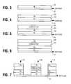
- FIG. 3is a cross-sectional elevation view of an antifuse and semiconductor layer formed during the fabrication of the invented array.
- FIG. 4illustrates the structure of FIG. 3 after an additional semiconductor layer has been formed.
- FIG. 5illustrates the structure of FIG. 4 after a conductive layer is formed.
- FIG. 6illustrates the structure of FIG. 5 after an additional semiconductor layer has been formed.
- FIG. 7illustrates the structure of FIG. 6 after a masking and etching step.
- FIG. 8illustrates the structure of FIG. 7 after open spaces left from the etching step have been filled.
- FIG. 9illustrates the structure of FIG. 8 after a planarization step.
- FIG. 10Aillustrates the structure of FIG. 9 after the recessing of the top silicon film below the fill dielectric.
- FIG. 10Billustrates the structure of FIG. 10 a after beveling the sidewalls of the fill dielectric.
- FIG. 10Cillustrates the structure of FIG. 10B after the deposition of a antifuse layer.
- FIG. 10Dillustrates the structure of FIG. 10C after the formation of a second plurality of rail stacks.
- FIG. 11Aillustrates the structure of FIG. 9 after the recessing of the top silicon film beneath the fill dielectric.
- FIG. 11Billustrate the structure of FIG. 11A after the beveling of the sidewalls of the fill dielectric.
- FIG. 11Cillustrates the structure of FIG. 11B after an antifuse layer is grown.
- FIG. 11Dillustrates the structure of FIG. 11C after the formation of a plurality of rail stacks.
- FIG. 12Aillustrates the structure of FIG. 9 after the recessing of the fill dielectric beneath the top silicon film of the rail stacks.
- FIG. 12B-1illustrates the structure of FIG. 12A after the deposition of an antifuse material.
- FIG. 12B-2illustrates the structure of FIG. 12A after an antifuse material is grown.
- FIG. 12C-1illustrates the structure of FIG. 12B-1 after a plurality of rail stacks are formed.
- FIG. 12C-2illustrates the structure of FIG. 12B-2 after the formation of a plurality of rail stacks.
- FIG. 13Aillustrates the structure of FIG. 9 after the recessing of the fill dielectric beneath the top surface of the rail stacks.
- FIG. 13Billustrates the structure of FIG. 13A after the sidewalls of the top silicon film of the rail stacks have been beveled.
- FIG. 13C-1illustrates the structure of FIG. 13B after the deposition of an antifuse material.
- FIG. 13C-2illustrates the structure of FIG. 13B after the antifuse materials is grown.
- FIG. 13D-1illustrates the structure of FIG. 13C-1 after the formation of a plurality of rail stacks.
- FIG. 13D-2illustrates the structure of FIG. 13C-2 after the formation of a plurality of rail stacks.
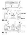
- FIG. 14Aillustrates the structure of FIG. 6 after the formation of an overlying hard masking layer.
- FIG. 14Billustrates the structure of FIG. 14A after the mask and silicon layers have been patterned.
- FIG. 14Cillustrates the structure of FIG. 14B after a dielectric filling material is formed.
- FIG. 14Dillustrates the structure of FIG. 14C after a planarization step.
- FIG. 14Eillustrates the structure of FIG. 14D after the hard mask has been removed and an antifuse layer of a thermally grown oxide has been formed.
- FIG. 14Fillustrates the structure of FIG. 14E after the formation of a plurality of rail stacks have been formed and where two of the three resulting cells are programmed by rupturing or breaching the thermally grown oxide layer.
- FIG. 15illustrates an alternate embodiment of the present invention where a deposited antifuse layer is formed after the filling step.
- FIG. 16Aillustrates another embodiment of the present invention where the filling material is filled above the level of the etched silicon lines.
- FIG. 16Billustrates the structure of FIG. 16A after planarization, the removal of a hard mask and the formation of an antifuse layer.
- the present inventionis a three-dimensional array which is field programmable.
- numerous specific detailsare set forth such as specific material and layer thicknesses. It will be apparent, however, to one skilled in the art that the present invention may be practiced without these specific details. In other instances, well-known circuits and fabrication techniques have not been set forth in detail in order not to unnecessarily obscure the present invention.
- the present inventionis a novel antifuse memory and its method of fabrication.
- the present inventionutilizes a surface treatment or a hard mask process to produce an antifuse structure which enhances antifuse performance by providing a more controllable and reliable programming (breakdown) voltage.
- the antifuse memory of the present inventioncomprises a first plurality of spaced apart rail-stacks having a top semiconductor material of a first conductivity type. A fill dielectric is formed between the individual rail-stacks.
- An antifuse material, such as silicon dioxide,is formed over the first plurality of rail-stacks.
- a second plurality of spaced apart rail-stacks having a lower semiconductor material of opposite polarity than the first semiconductor materialis then formed over the antifuse layer and over the first plurality of spaced apart rail-stacks and the fill dielectric.
- the second plurality of spaced apart rail-stacksis generally in a direction perpendicular to the first plurality of spaced apart rail-stacks. Each of the intersections of the first rail-stacks and the second rail-stacks generate an antifuse memory cell.
- the cellsare programmable by providing a relatively high voltage (5-20 volts) between the rail-stacks of a given memory cell so as to forward bias the diode created by using semiconductor materials of different conductivity types in the first and second spaced apart rail-stacks.
- the relatively high voltagecauses a breach or rupture in the antifuse layer which creates a diode. Without the high voltage the antifuse layer remains an insulator.
- diodescan be selectively formed so as to program the array.
- a surface treatment or hard mask processis used to insure that all memory cells of the array can be programmed at substantially the same voltage by controlling the locations at which the antifuse material ruptures and/or by controlling the thicknesses uniformity of the antifuse material.
- a short semiconductor material etchis used prior to antifuse deposition or growth in order to slightly recess the semiconductor material below the top surface of dielectric fill between the spaced apart rail-stacks.
- the semiconductor materialis recessed to a fraction of the thickness of which a deposited antifuse material is to be formed so that the antifuse material can be deposited uniformly on the semiconductor region.
- the semiconductor materialcan be recessed to a depth greater than the thickness of the antifuse material and than the antifuse material grown on the semiconductor film.
- the antifuse materialis confined between adjacent fill dielectrics thereby creating a uniform thickness antifuse film across the semiconductor material surface.
- the antifuse materialis formed to a uniform thickness between the semiconductor materials of the first and second rail-stacks thereby enabling a more uniform and reproducible programming of the antifuse across the memory array.
- the fill dielectricis recessed below the top surface of the semiconductor material prior to antifuse deposition.
- a convex corner or protrusionis generated in the semiconductor material.
- the antifusealways “blows” or ruptures at the corner of the semiconductor material because of the high electric fields experienced at the corner. Because each antifuse blows at the corner, each cell will have substantially the same programming voltage.
- a slight recess etch of the fill dielectric or of the semiconductor materialis done prior to antifuse deposition or growth in order to generate antifuse cells which are programmed at the same voltage.
- Controlling the sigma of the breakdown voltage of an antifuseis extremely valuable in that it allows one to reduce the margin between write and read, reducing the voltage required from drivers, thus reducing their power and therefore the amount of substrate area they require. Additionally, limiting the total area at the critical thickness of the antifuse increases both yield and reliability.
- a hard maskis used during rail stack patterning and as a polish stop during chemical mechanical planarization (CMP) of the gap fill dielectric.
- CMPchemical mechanical planarization
- the height of the gap fill dielectricis selected in order to affect the protrusion or recession of the array line once the hard mask is stripped.
- the protrusion or recessionis selected in order to manipulate the antifuse rupture (i.e., cell programming) process.
- the invented memory arrayis fabricated on several levels and, for instance, may have eight levels of storage.
- Each levelincludes a first plurality of parallel spaced-apart rail-stacks running in a first direction and a second plurality of rail-stacks or conductors (depending on the embodiment) running in a second direction.
- the first rail-stacksrun perpendicular to the second conductors/rail-stacks and hence form a right angle at their intersections.
- rail-stacksare a departure from prior art three-dimensional memories where conductors alone were used in lieu of rail-stacks, and where discrete cells (e.g., pillars) were formed at the intersections of the lines.
- discrete cellse.g., pillars
- a bitis stored at each of the intersections of rail-stacks.
- memory cellsare defined by the rail-stacks and intermediate layers. This makes it easier to fabricate the invented array as will be seen. When the array is fabricated all the bits are in the zero (or one) state and after programming, the programmed bits are in the one (or zero) state.
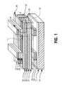
- FIG. 1several rail-stacks are illustrated in the partial cross-section of the invented array.
- rail-stack 16is shown at one height and a half rail-stack 18 is shown at a second height above the first height.
- half rail-stacksare disposed between rail-stack 16 and a substrate 10 .
- These lower rail-stacksrun in the same direction as the half rail-stack 18 .
- a bitis stored at the intersection of rail-stacks and, for instance, a “cell” is present between the rail-stacks and layers shown within the bracket 17 and another within the bracket 19 .
- Each of these bracketsspan a memory level.
- the arrayis fabricated on a substrate 10 which may be an ordinary monocrystaline silicon substrate.
- Decoding circuitry, sensing circuits, and programming circuitsare fabricated in one embodiment within the substrate 10 under the memory array using, for instance, ordinary MOS fabrication techniques. Vias are used to connect conductors within the rail-stacks to the substrate to allow access to each rail-stack in order to program data into the array and to read data from the array.
- the circuitry within the substrate 10may select rail-stack 16 and the rail stack 18 in order to either program or read a bit associated with the intersection of these rail-stacks.
- an insulating layer 12is formed over the substrate in order that the array may be fabricated above the substrate.
- This layermay be planarized with, for instance, chemical-mechanical polishing (CMP) to provide a flat surface upon which the array may be fabricated.
- CMPchemical-mechanical polishing
- a conductive layer 14is formed on the substrate.
- conductive layersare used within the rail-stacks and these layers and the resultant conductors may be fabricated from elemental metals such as tungsten, tantalum, aluminum, or copper, or metal alloys may be used, such as MoW.
- Metal silicidesmay also be used such as TiSi 2 , or COSi 2 , or a conductive compound such as TiN, or WC may be used.
- a highly doped semiconductor layer such as siliconis also suitable. Multiple layer structures may be used selecting one or more of the above.
- a layer of semiconductor materialsuch as silicon is formed over the conductive layer.
- Thisis typically a polysilicon layer; however, an amorphous layer may be used.
- Other semiconductor materialsmay be used such as Ge, GaAs, etc.
- this semiconductor layeris highly doped and, as will be seen, forms one-half a diode.
- half rail-stacksare formed. These rail-stacks are “half” or partial rail-stacks since they are approximately half the thickness of the rail-stacks used in the next level.
- the layer 20is a dielectric such as silicon dioxide which is deposited by chemical vapor deposition (CVD) in a blanket deposition over the half rail-stacks and over a dielectric fill which fills the spaces between the rail-stacks.
- CVDchemical vapor deposition
- the layer 20is grown on the upper surface of the silicon layer 15 and only exists on the rail-stacks.
- a full set of memory array rail-stacksis formed on the layer 20 .
- Thiscomprises first the deposition of a lightly doped silicon layer 21 doped with a conductivity type dopant opposite to that used for the silicon layer 15 , a heavily doped silicon layer 22 doped also opposite to the layer 15 , a conductive layer 23 and a heavily doped silicon layer 24 doped with the same conductivity type dopant as layers 21 and 22 .
- the rail-stacks shown in FIG. 1, such as rail-stack 16are formed. These rail-stacks are, as illustrated, in a direction perpendicular to the rail-stacks above and below them.
- the spaces between the rail-stacks after they are definedare filled with a dielectric such as silicon dioxide.
- a dielectricsuch as silicon dioxide.
- the rail-stacks and fillare planarized by CMP.
- spin-on-glass (SOG)is used to fill the voids.
- chemical planarizationcan be used, for example, plasma etching.
- Other fill and planarization methodscan be used.
- another antifuse layer 26is formed, for instance, from a dielectric such as silicon dioxide, silicon nitride, silicon oxynitride, amorphous carbon or other insulating materials or combinations of materials. (Also an undoped layer of silicon may be used for the antifuse layer.)
- This half rail-stackcomprises a silicon layer 28 doped with a conductivity type dopant opposite to that of layer 24 . This is a lightly doped layer.
- Another silicon layer 30is formed on layer 28 and this layer is doped with the same conductivity type dopant as layer 28 , however, it is more heavily doped. Then a conductive layer 31 is formed above the layer 30 .
- Half rail-stacksare used at the very upper-most level of the array and at the very lowest level of the array. In between the half rail-stacks the full rail-stacks, such as rail-stack 16 , are used throughout the array. If desired, a full rail stack can be used for the uppermost level of the array.
- the silicon layers disposed on the conductive layersextend the entire length of the rail-stacks in the embodiment of FIG. 1 and are uninterrupted except possibly where vias are used to provide a conductive path to the substrate 10 .
- a path 32is illustrated from a lower conductor in level 17 to an upper conductor in this level found in the rail-stack 18 .
- This pathis accessed in one embodiment through decoding circuitry in the substrate for both programming and reading of data into and from the array for one bit.
- a relatively high voltage5-20V is applied between the conductors generally so as to forward-bias the “diode” between these conductors.
- This relatively high voltagecauses a breach in the layer 26 creating a diode. Without this high voltage, the layer 26 remains an insulator.
- diodescan be selectively formed so as to program the array. While programming the array with the layers adjacent to the antifuse material being forward-biased is currently preferred, it is also possible to program using a reverse-biasing potential.
- a voltage lower than that for programmingis used. This voltage is applied so as to forward-bias the diode of the cell being accessed and thus allowing a sense amplifier to determine whether or not the layer 26 is intact between the rail-stacks. Note that “sneak” or parasitic paths in the array which would interfere with the sensing will include a reverse-biased diode.
- the “anode” and “cathode” of the diodesare reversed at each of the successive antifuse layers. This facilitates easier programming and sensing since all of its conductors at each level are either bit lines or word lines. And, for instance, conductors at one height will serve as bit lines for two levels and conductors at the next height serve as word lines for two levels. This simplifies the decoding and sensing and more importantly reduces processing.
- FIG. 2In the cross-section elevation view of FIG. 2, one embodiment is illustrated which corresponds to the embodiment shown in FIG. 1 .
- the half rail-stacks of FIG. 1are not illustrated.
- Three complete levels 35 , 36 and 37 of the arrayare illustrated in FIG. 2 .
- Below layer 38 of FIG. 2other rail-stacks or half rail-stack are used.
- Also above layer 65a full or half rail-stack is used.
- the rail-stack 3comprising layers 38 through 41 includes a lightly doped N ⁇ layer 38 , a heavily doped N+ layer 39 , a conductor layer 40 and N+ layer 41 .
- An antifuse layer 42which for the embodiment of FIG. 3 is a blanket deposition, covers all of the rail-stacks formed below layer 42 as well as the fill filling the voids between the rails.
- the layer 42can be a deposited silicon dioxide in one embodiment.
- N+ layerssandwich the conductor layer 40 . These highly doped layers provide ohmic transitions to prevent unintended Schottky diode formation.
- the layers above and below conductor 40are not symmetrical for the embodiment illustrated in that an N ⁇ layer 38 is used below the conductor 40 and not above the conductor 40 . Only a single lightly doped layer (in conjunction with a heavily doped layer) is needed to define a diode; the thickness of this lightly doped layer is important in controlling the break-down voltage, reverse leakage current and resistance of the diode so formed.
- the layer 41 , a heavily doped semiconductor layer, and the fillare planarized after the rail-stacks are defined and then a blanket deposition of the antifuse layer 42 is formed on the layer 41 . It is important to ensure that the planarization step exposes layer 41 everywhere so that the devices work properly. (The lines 43 in FIG. 2 are used to indicate that the antifuse layer 42 and like layers are not etched with the rail-stack below it and thus extend over the entire array for the illustrated embodiment.)
- layer 42 and the other like layers in the structuresuch as layers 51 , 56 and 65 , is that since they are an unbroken deposition, sidewall leakage (into the rail-stacks below) will be minimized, limiting electrical problems during reading and writing.
- subsequent conductive materialis deposited, it is unable to reach the sides of the rail-stacks below it because of this blanket deposition of the antifuse layer.
- path 49which would allow silicon from layer 52 to cause a parasitic path, does not exist because of the unbroken blanket deposition of the antifuse layer 51 .
- Rail-stacks 4comprising layers 44 , 45 , 46 and 47 are formed on the antifuse layer 42 .
- Layer 44is lightly doped with a P-type dopant for the embodiment illustrated followed by a P+ layer 45 , a conductive layer 46 and a P+ layer 47 .
- these layersare deposited, they are masked and etched to define the rail-stacks.
- the voids between these rail-stacks, such as void 50are filled with a dielectric.
- the fill dielectricis planarized along with a portion of P+ layer 47 . Planarization is done at this point in the fabrication since there is generally poor control over the thickness and contour of the fill.
- the filltends to build up on the rail-stacks when a non-spin-on deposition is used. This is followed by a blanket deposition of layer 51 .
- path 66when a large enough voltage is applied between conductors 46 and 54 , the antifuse layer 51 , at the intersection of layers 47 and 52 , is breached or ruptured creating a diode at the intersection. As mentioned, this is selectively done throughout the array to program the array.
- the conductor 54is therefore a bit line for the “cells” above and below it.
- path 67indicates another possible current path for another “cell” where the conductor 54 is again a bit line during sensing.
- planarizationalways occurs on a heavily doped layer such as layer 47 and layer 55 .
- lightly doped layersare always formed on relatively planar surfaces, consequently their thickness can be more easily controlled. This, as mentioned, allows the characteristics of the diode (once the intermediate antifuse layer is breached) to be more reliably controlled.
- FIGS. 3-13The process flow for forming rail-stack 5 of FIG. 2 is illustrated in FIGS. 3-13. It will be apparent that the rail-stacks for the other embodiment can be similarly processed.
- an antifuse layer 51is deposited. This typically is 25-200 ⁇ of silicon dioxide which can be deposited with any one of very well-known processes. Following this, a silicon layer 52 is deposited which is typically 1000-4000 ⁇ thick and formed with a CVD process where a phosphorous dopant is deposited along with the deposition of for instance, the polysilicon semiconductor material or where the dopant is ion implanted following the deposition of the layer. This layer is doped to a level between 5 ⁇ 10 15 -1 ⁇ 10 18 /cm 3 .
- polysilicon layersmay be deposited as polysilicon or may be formed from an amorphous silicon layer.
- an amorphous silicon layeris deposited and annealed in a rapid thermal anneal (RTA) step of 800° C. for 1 minute. This increases the crystal sizes and activates the dopant.
- RTArapid thermal anneal
- the dopantcan be ion implanted or introduced during the deposition of the amorphous silicon layer.
- a N+ layer 53is deposited again using CVD.
- This layermay be approximately 300-3000 ⁇ thick and in one embodiment is doped to a level of >10 19 /cm 3 .
- layers 52 and 53are often shown such as layers 52 and 53 , with different doping. These layers may be formed in one deposition by changing the dopant concentration during an in-situ deposition process. Alternatively, these layers may be formed with one deposition, followed by an ion implantation step at two different energy levels and dosages to obtain the two doping levels.
- a conductive layerwhich may be 500-1500 ⁇ thick is formed using any one of numerous well-known thin film deposition processes such as sputtering.
- a refractory metalmay be used or a silicide of a refractory metal.
- aluminum or coppercan be used, or more simply the heavily doped silicon can be the conductor.
- another semiconductor layer of, for instance, polysilicon approximately 1500-2000 ⁇ thickis formed again doped to a level of >10 19 /cm 3 .
- Thisis shown as layer 55 in FIG. 6; after planarization its thickness is between 300 ⁇ and 2000 ⁇ thick.
- a masking and etching stepis now used to define rail-stacks, such as rail-stacks 69 , 70 and 71 shown in FIG. 7 .
- rail-stackssuch as rail-stacks 69 , 70 and 71 shown in FIG. 7 .
- An ordinary masking and etching stepfor instance, photolithography followed by plasma etching, may be used.
- Etchantscan be used that stop on the antifuse layer thus preventing this layer from being etched away.
- layer 51can be considered an etchant stop layer depending on the specific etchants used.
- the spaces between the rail-stacksare filled with a dielectric 72 such as formed with a high density plasma chemical vapor deposition (HDPCVD) process.
- a dielectric 72such as formed with a high density plasma chemical vapor deposition (HDPCVD) process.
- Chemical-mechanical polishingis then employed to planarize the upper surface of the rail-stacks shown in FIG. 9 in one embodiment.
- Chemical etchingcan also be used as mentioned with certain dielectrics.
- This planarizationcan reduce the thickness of the layer 55 to approximately 300 ⁇ , thus this layer ends up being of approximately the same thickness as the layer 53 .
- the substratehas a planarized surface 75 whereby the top surface of the N+ regions of the rail stacks 69 , 70 and 71 are substantially planar with the top surfaces of dielectric fill 72 .
- FIGS. 10A-10DA surface treatment in accordance with a first embodiment of the present invention is set forth in FIGS. 10A-10D and the accompanying description.
- the substrateis subjected to a short silicon etch so that the top surface 80 of the top N+ silicon film 55 is slightly recessed below the top surface 82 of the fill dielectric 72 to form a recess 84 which is bounded by sidewalls 86 of fill dielectric 72 as shown in FIG. 10 A.
- the top surface 80 of the N+ silicon film 55is recessed approximately 5-150 ⁇ below the top surface 82 of the dielectric fill material 72 .
- the recesshas a depth which is a fraction of the thickness desired for antifuse material 56 .
- Recess 84can be formed utilizing any well-known etchant or technique which can preferentially etch the silicon film 55 with respect to fill dielectric 72 (i.e., use a silicon etch which is selective to the fill dielectric 72 ).
- the silicon etchis a nonpolymer forming etchant so that the silicon surface 80 stays atomically clean.
- a nonpolymer forming silicon recess etch which is selective to an oxide fill dielectriccan be accomplished utilizing a NF 3 plasma etch or a CF 4 and O 2 plasma etch.
- the silicon recess etchis accomplished utilizing a wet etch such as a wet etch comprising nitric acid and hydrofluoric acid or a wet etch comprising KOH.
- the silicon recess etchis followed by a short sputter etch to shape the sidewall 86 of the oxide fill 72 into a sloped sidewall 88 as shown in FIG. 10B.
- a slopped sidewall 88allows the subsequently deposited antifuse material 56 to be more uniform as it transitions from the fill dielectric to the silicon surface 80 .
- the sputter etchcan be used to remove contaminants. During sputter etching, care should be taken not to roughen the surface 80 of the silicon film 55 too much and thereby create nonuniformities across the surface 80 .
- a sputter etch which removes 25-50 ⁇ SiO 2such as a sputter etch with Argon ions with between 100-1000 volts bias and a pressure between 0.1-5.0 mtorrs, is suitable.
- the antifuse material 56is blanket deposited over and onto surface 80 of silicon film 55 and surface 82 and sidewall 88 of dielectric fill 72 .
- the antifuse material 56is deposited to a thickness which is sufficient to completely fill recess 84 with antifuse material.
- Completely filling the recess 84 with antifuse material 56helps to insure uniform film coverage over a corner 89 of the silicon film which helps to prevent electric field enhancement at the silicon corner 89 .
- the antifuse material 56 over the silicon corner 89is at least as thick as the antifuse material 56 formed on horizontal silicon surfaces.
- the deposited antifuse materialis an oxide.
- a deposited oxide antifuse materialcan be formed by a plasma enhanced chemical vapor deposition (PECVD) process utilizing a deposition chemistry comprising SiH 4 and O 2 .
- PECVDplasma enhanced chemical vapor deposition
- a deposited oxide antifuse 56can be a thermally deposited oxide such as a low temperature oxide (LTO) deposited by thermal disassociation of SiH 4 and O 2 at a temperature between 350-600°.
- LTOlow temperature oxide
- a deposited oxide antifusecan be a high temperature oxide (HTO).
- a plurality of rail stacks 6are formed on antifuse material 56 .
- a lower P ⁇ type silicon film 61is blanket deposited over and onto antifuse material 56 followed by the sequential blanket deposition of a P+ type silicon film 62 , conductor 63 , and a P+ type silicon film 64 .
- the p type silicon films ( 61 , 62 and 64 )can be formed by the same technique and to the same thickness and concentrations, but by utilizing opposite conductivity type dopants (e.g., boron) as n type silicon films 52 , 53 and 55 of rail stack 5 .
- Conductor 63can be formed over the same material and to the same thickness and by the same technique as conductor 54 .
- the films of rail stack 6would then be patterned by well-known photolithography and etching techniques into a plurality of spaced-apart rail stacks which run in a direction perpendicular to the plurality of rail stacks ( 69 , 70 and 71 ) of rail stacks 5 .
- a fill 60would then be formed over and between the plurality of spaced-apart rail stacks 6 and planarized the form a planar surface.
- the planar surfacewould then be treated in accordance with the surface treatment of the present invention to improve the uniformity and performance of subsequently formed antifuse 65 .
- FIGS. 11A-11DA surface treatment in accordance with another embodiment of the present invention is set forth in FIGS. 11A-11D.
- first surface 80 of silicon film 55is etched below surface 82 of the fill dielectric 72 so that a recess 88 is formed which is bounded by sidewalls 86 of fill dielectric 72 .
- the recess 84is formed to a depth which is greater than the thickness desired of the antifuse material 56 .
- Recess 84can be formed by techniques and with etchants as described above.
- the silicon recess etchcan be followed by a sputter etch as described above to produce sloped sidewalls 88 as shown in FIG. 11 B.
- an antifuse materialis grown on silicon surface 80 of recess 84 .
- An oxide antifuse material 56can be grown by exposing the substrate to an oxidizing ambient such as O 2 or H 2 O (without a silicon source gas) while heating the substrate or creating a plasma. Such a processes will selectively grow silicon dioxide on locations where silicon is available to oxidize, such as silicon surface 80 , and will not grow on locations, such as fill dielectric 72 , where silicon is unavailable for oxidation.
- antifuse 56is an oxide grown by exposing the substrate to a high density plasma (HDP) formed from O 2 molecules.
- HDPhigh density plasma
- a suitable grown oxide antifuse 56can be formed by a thermal process, such as a furnace oxidation in a wet ambient such H 2 O, or a rapid thermal oxidation utilizing an O 2 ambient. Because the silicon surface 80 is sufficiently recessed below the surface 82 of the fill dielectric 72 and because the antifuse material 56 is grown, as opposed to deposited, the grown antifuse oxide is constrained by the sidewalls 88 of recess 84 . In this way, an antifuse material 56 is formed which has a very uniform thickness across the surface 80 of the N+ silicon film 55 . A uniform antifuse film 56 across the surface of N+ silicon film 55 helps insure a uniform and reliable antifuse programming and performance. Although forming sloped sidewalls is not required, they are especially useful when growing an oxide by a high density process because corners can become charged or create shadowing which can create deflections in the ionized oxygen atoms leading to nonuniform film growth.
- a plurality of the rail stacksare formed over and onto antifuse material 56 as well as onto the surface of dielectric fill material 72 .
- Rail stacks 6can be formed as described above.
- FIGS. 12 A- 12 C- 1 and 12 C- 2detail an alternative surface treatment in accordance with an embodiment of the present invention.
- the substrate of FIG. 9is subjected to a short dielectric etch which etches away the top of the dielectric film so that the top surface 90 of the fill dielectric 72 is recessed below the top surface 92 of the upper N+ silicon film 55 of rail stack 5 to form a recess 94 which is bounded by the sidewalls 96 of the silicon film 55 .
- the dielectric fill materialis recessed below silicon surface 92 so that a convex corner or protrusion 97 is formed at the top edge of the N+ silicon film.
- the top surface 90 dielectric fill material 72is recessed between 50-200 ⁇ below the top surface 92 of silicon film 55 .
- the fill dielectric 72can be recessed with any well-known etchant which can preferentially etch the fill dielectric without substantially etching silicon film 55 (i.e., recess is formed with a fill dielectric etch that is selective to silicon). If the fill dielectric is an oxide and if the top semiconductor material is silicon then a plasma etch comprising CHF 3 and O 2 can be used. Preferably, a wet etch comprising HF and H 2 O can be used.
- the antifuse material 56is formed onto and over the surface 92 , corner 97 , and sidewalls 96 of semiconductor material 55 .
- the antifuse material 56is a deposited oxide formed to a thickness between 20-80 ⁇ .
- a deposited oxide antifuse filmcan be formed as described above.
- the antifuse 56 in FIG. 12B-1is deposited, it is also forms on surface 90 of recessed fill dielectric 72 as shown in FIG. 12B-1.
- the antifuse materialis an oxide grown to a thickness between 20-80 ⁇ . Because the oxide is grown, it forms only on exposed silicon regions, such as surface 92 , corner 97 , and sidewalls 96 and does not form on surface 90 of fill dielectric 72 as shown in FIG. 12B-2.
- a plurality of rail stacksare formed onto antifuse material 56 .
- the rail stackis formed on the antifuse on the silicon film 55 and fill dielectric 72 .
- a grown antifuseis used, it forms on the antifuse on the silicon film and forms on the fill dielectric 72 as shown in FIG. 12C-2.
- Rail stacks 6can be formed as described above. It is to be appreciated that as shown in FIGS. 12C-1 and 12 C- 2 , the corner 97 of the N+ silicon extends above the fill dielectric.
- Such a protruding cornercreates a high electric field at the corner during programming.
- the antifuse material 56will always “blow” or rupture at the region 99 above corner 97 . Because the antifuse material 56 always “blows” or ruptures at corner 97 , a thicker antifuse film can be used which lowers the overall leakage of the cell while still retaining a low breakdown (programming) voltage.
- FIGS. 13 A- 13 D- 1 and 13 D- 2detail another surface treatment in accordance with another embodiment of the present invention.
- the fill dielectricis recessed below the top surface of the N+ silicon film 55 to form a recess 94 and expose corner 97 of the N+ silicon film.
- the fill dielectriccan be recessed as described with respect to FIG. 12 A.
- a sputter etchis used to chamfer or bevel corner 97 .
- a sputter etchhas a higher yield at an angle of approximately 45° to the surface of the substrate creating a beveled corner 95 in silicon film 55 having a slope at an angle of approximately 45°.
- a sputter etch processwhich has 25-50 ⁇ SiO 2 equivalent removal can be used, such as the sputter etch described above.
- the antifuse film 56is formed on top of surface 92 and on beveled corner 95 .
- the antifuse materialis a deposited oxide formed to a thickness between 20-80 ⁇ .
- a deposited oxide antifuse filmcan be formed as described above.
- the antifuse film 56is deposited, it also forms on surface 90 of recess fill dielectric 72 as shown in FIG. 13C-1.
- the antifuse materialis a grown oxide grown to a thickness between 20-80 ⁇ .
- oxide antifuseBecause the oxide antifuse is grown, it forms only on exposed silicon regions, such as surface 92 and beveled corner 95 , and does not form on surface 90 of fill dielectric 72 as shown in FIG. 13C-2.
- An oxide antifuse filmcan be grown as described above.
- a plurality of rail stack 6are formed onto and over antifuse material 56 .
- Rail stackscan be formed as described above.
- the plurality of rail stack 6is formed on the antifuse material on the silicon film 55 and on the antifuse on fill dielectric 72 .
- the plurality of rail stacksare formed on the antifuse material on the silicon surface 92 and directly onto the surface 90 of fill dielectric 72 .
- FIGS. 14A-14F and FIG. 15 and FIG. 16A-16Bdetail an embodiment of the present invention where a hard mask is used to create recessed fill dielectrics (to create silicon protrusions) or recessed silicon films to ensure that all memory arrays can be programmed at substantially the same voltage by controlling the location at which the antifuse material ruptures and/or by controlling the thickness and uniformity of the antifuse material.
- a thin (e.g., 1500 ⁇ ) silicon nitride (SiN x ) layeris deposited above a silicon layer by plasma enhanced chemical vapor deposition (PECVD), and used as both a hard mask during array patterning and a polish stop during chemical-mechanical planarization (CMP).
- PECVDplasma enhanced chemical vapor deposition
- CMPchemical-mechanical planarization
- the masking layermay be deposited in a LPCVD furnace.
- a thin (e.g., 200 ⁇ ) buffer oxide layercan be formed on the silicon layer prior to the silicon nitride layer to protect the underlying silicon layer.
- the use of SiN x as an etch hard mask as well as a CMP stopping layeris a well established component of the shallow trench isolation (STI) manufacturing process.
- STIshallow trench isolation
- the process flow corresponding to an embodimentis as follows: (1) blanket deposition of array rail-stack materials, culminating with a SiN x film; (2) photolithography used to delineate array features; (3) array patterning by plasma etching using the SiN x layer as a hard mask (note that additional benefits of the hard mask may include better CD control over the non-hard mask case); (4) gap fill, typically with HDP-CVD silicon dioxide, where the height to which the gaps are filled can be chosen carefully as will be discussed below; (5) CMP, with the SiN x acting as the polish stop, using a CMP slurry that erodes silicon dioxide at a much faster rate than SiN x such as a silica slurry or ceria (CeO 2 ) slurry; (6) post-CMP clean typically in an NH 4 OH-based scrub; (7) SiN x removal via plasma or wet etching; and (8) growing or CVD blanket deposition of an antifuse layer.
- the spaces of the line/space arraysare filled with silicon dioxide.
- the height of the fill for these spacesis selected in order to effect the protrusion or recession of the array lines in the antifuse layer once the SiN x is stripped. That is, if the gap fill target height corresponds to the lower edge of the SiN x layer, no protrusion or recession is targeted. If a line recession is desired, the gap is filled to a point above the lower edge of the SiN x layer, with the absolute fill height a function of the degree of recession desired. If a line protrusion is desired, the gap is filled to a point below the lower edge of the SiN x layer, with the absolute fill height again a function of the degree of protrusion desired.
- a protrusion or recession(or lack thereof) is selected in order to manipulate the antifuse rupture (i.e., cell programming) process.
- a uniform protrusion or recession of array lines over the wafer surfacemay result in more repeatably programmable memory cells due to electric field concentration at the protrusion or recession corners.
- devices constructed this wayare more reliable.
- the hard mask embodimentwill be described with respect to the formation of the antifuse devices formed between the intersections of the fifth and sixth rail stacks of FIG. 2 . Accordingly, processing occurs as set forth in FIGS. 3-6.
- a hard mask layer 111is formed on the silicon film 55 as shown in FIG. 14 A.
- the layer 111may be formed from material such as silicon nitride to a thickness of 1500 ⁇ .
- Other materials that may be used as the hard mask layer 111include but are not limited to TiN, tungsten, and tungsten silicide (WSi 2 ).
- the layer 111should be of a hard material, that is, a material that erodes more slowly than the dielectric filling material used in a subsequent step. As will be seen the layer 111 , after patterning, acts as a polish stop for a planarization step. Typically, the hard masking layer 111 will include a lower thin (25-200 ⁇ ) buffer oxide layer to protect the silicon.
- the layer 111After the layer 111 as been formed, it is patterned using ordinary photolithographic steps to form a mask.
- the layer 111defines parallel spaced-apart lines. This is shown in FIG. 14B where the layer 111 , after patterning includes the masking features 111 a , 111 b and 111 c . Additionally, as shown in FIG. 14B the films of rail stacks are etched in alignment with the mask forming the lines 70 , 69 and 71 . Spaces 113 result between the lines as shown in FIG. 14 B.
- the spaces 113 between the lines 70 , 69 , and 71are filled with a dielectric material 72 , such as a CVD formed silicon dioxide or other dielectric material.
- a dielectric material 72such as a CVD formed silicon dioxide or other dielectric material.
- This materialis chosen to be softer than the masking layer 111 , as mentioned.
- An important exampleis the use of a CMP slurry that is selective to silicon dioxide over the silicon nitride. That is, the erosion rate of silicon dioxide is much greater than that of silicon nitride using such slurry.
- the fill 72 as shown in FIG. 14Cis filled to a level below the upper surface of the rails 70 , 69 , and 71 . This is shown by dimension 116 .
- the fillis between 50-500 ⁇ below the upper surface of rails 70 , 69 , and 71 .
- Fill 72accumulates on the tops of the masking members as a result of filling the dielectric material between the lines. Well-known processing steps are used to assure the desired height of the fill between the lines.
- planarizationoccurs which removes the dielectric material from the upper surfaces of the masking members. While chemical planarization may be used, in one embodiment chemical-mechanical polishing (CMP) is preferred.
- CMPchemical-mechanical polishing
- the etchants used in such planarizationare selected from commercially available etchants such that the dielectric material is eroded without significant etching of the mask. In effect, the mask acts as an erosion stop for the resultant structure shown in FIG. 14 D. Note that the erosion does not significantly affect the fill level between the lines and that the fill 72 between the lines remains below the upper surface as shown by dimension 116 in FIG. 14 D.
- the mask 111 a , 111 b , and 111 cis removed using, for instance, an ordinary step which selectively removes the silicon nitride without disturbing the underlying silicon and the fill 72 .
- a hot phosphoric acid stripcan remove the silicon nitride mask.
- a HF dipcan then be used to remove the thin buffer oxide, if used.
- a thermally grown oxideis grown on the exposed upper surface of silicon film 55 of the lines 70 , 69 , and 71 .
- this oxideis grown at a temperature of 600° C. in a steam atmosphere for one hour. This results in an antifuse layer 56 of silicon dioxide having a nominal thickness of 50 ⁇ .
- FIG. 14EThe resultant structure of FIG. 14E is shown by the silicon film 55 of the lines 70 , 69 , and 71 protruding from the fill material. This protrusion assists in providing the enhanced programming. As shown within the circle 120 of FIG. 14E, when the oxide is thermally grown it tends to be slightly thinner at the corners or edges of the polysilicon lines when compared to the central portion of the lines.
- the silicon films of rail stack 6are formed over the structure of FIG. 14 E and patterned into transverse spaced-apart lines lying above the structure of FIG. 14E as shown in FIG. 14 F.
- a memory cellis formed where each of the lines 70 , 69 , and 71 project into the sixth rail.
- Each cellhas an antifuse layer (silicon dioxide layer 56 ) disposed between the P type and the N type halves of a diode.
- the diodeis forward biased with a potential great enough to rupture or breach the silicon dioxide layer. This causes a conductive path during memory read cycles through the cell when the diode is forward biased at a potential lower than that needed to program the cell.
- the breaks 122 and 123 in the layer 56indicate that the cells associated with lines 70 and 71 are programmed.
- the layer 56 associated with the line 69remains intact indicating that this cell is not programmed.
- two of the cellsmay be considered to be programmed with a binary 1 with the other containing a binary 0.
- the ruptures 122 and 123 in layer 56occur at the corners of the protruding silicon films of lines 70 and 71 , respectively.
- the reason this occursis because of the enhanced electric field associated with the edges of the lines and the thinner region of the layer 56 which occurs during its growth at the edges as shown within the circle 20 of FIG. 14 E. Both of these factors or at least one of them is present to assist in programming.
- FIG. 15Another hard mask embodiment is shown in FIG. 15 .
- the silicon lines 69 , 70 and 71 along with the fill 72are formed in the same manner as the corresponding structure shown in FIG. 14D, and the hard mask is removed.
- a deposited silicon dioxide layeris used.
- a plasma-enhanced CVD silicon dioxide layer 56is then deposited on the substrate.
- This layeralso covers the fill 72 unlike the grown oxide of FIG. 14 E.
- This embodimenthas the advantage of not requiring the higher temperature needed for growing an oxide.
- the silicon film 55 of lines 70 , 69 , and 71protrude from the fill 72 . As shown within the circle 137 , the side of the line 71 protrudes into a thinner oxide region.
- the deposited oxidetends to be thinner on the sidewalls of the rails than on the top surface of the rails or on the fill dielectric as shown in FIG. 15, due to shadowing by the corners during deposition.
- the antifuse layertends to open along the protruding line closer to the fill rather than at the corner of the line when programmed.
- this embodimentis similar to the prior embodiment except that a deposited antifuse layer is used.
- FIGS. 16A and 16Bshow yet another hard mask embodiment where rather than protrusions, recessions in the antifuse layer in the central region of the polysilicon lines occur.
- the silicon layeris etched using a hard mask which is first patterned as shown by the masking features 144 A, 144 B and 144 C and the polysilicon line 70 , 69 and 71 , respectively of FIG. 16 A.
- the spaces between the linesare then filled with a fill material 72 , again a material which is softer than the mask, this time however, to a level above the lower surface of the hard mask.
- the fill 72is above the upper surface of the hard mask by for instance, 1000 ⁇ .
- the fillaccumulates on the hard mask as shown by the dielectric material 145 .
- CMP or other planarizationis used to planarize the wafer, with the mask acting as a stop. Now the mask is removed with a selective etchant which selects the silicon nitride over the thin silicon dioxide buffer film and silicon dioxide filling material.
- the resultant structureincludes fill which is higher than the corresponding lines as shown in FIG. 16B.
- a silicon dioxide antifuse layer 56is deposited or grown over the wafer. When the antifuse is deposited by, for example PECVD, this results in a thinner silicon dioxide at the fill/silicon line interface 154 as shown within circle 151 and a thicker antifuse in the region of the silicon lines between the edges of the line as shown by dimension 152 . This may be used where it is desired, by way of example, to cause a breach of the antifuse during programming to occur at the edge 152 of the line.
- the inventionprovides a more reliable cell, particularly from the programming standpoint.
Landscapes
- Physics & Mathematics (AREA)
- Condensed Matter Physics & Semiconductors (AREA)
- General Physics & Mathematics (AREA)
- Engineering & Computer Science (AREA)
- Computer Hardware Design (AREA)
- Microelectronics & Electronic Packaging (AREA)
- Power Engineering (AREA)
- Semiconductor Memories (AREA)
- Design And Manufacture Of Integrated Circuits (AREA)
Abstract
Description
Claims (58)
Priority Applications (2)
| Application Number | Priority Date | Filing Date | Title |
|---|---|---|---|
| US09/746,083US6541312B2 (en) | 2000-12-22 | 2000-12-22 | Formation of antifuse structure in a three dimensional memory |
| US10/114,451US6768185B2 (en) | 2000-12-22 | 2002-04-01 | Formation of antifuse structure in a three dimensional memory |
Applications Claiming Priority (1)
| Application Number | Priority Date | Filing Date | Title |
|---|---|---|---|
| US09/746,083US6541312B2 (en) | 2000-12-22 | 2000-12-22 | Formation of antifuse structure in a three dimensional memory |
Related Child Applications (1)
| Application Number | Title | Priority Date | Filing Date |
|---|---|---|---|
| US10/114,451DivisionUS6768185B2 (en) | 2000-12-22 | 2002-04-01 | Formation of antifuse structure in a three dimensional memory |
Publications (2)
| Publication Number | Publication Date |
|---|---|
| US20030003632A1 US20030003632A1 (en) | 2003-01-02 |
| US6541312B2true US6541312B2 (en) | 2003-04-01 |
Family
ID=24999410
Family Applications (2)
| Application Number | Title | Priority Date | Filing Date |
|---|---|---|---|
| US09/746,083Expired - LifetimeUS6541312B2 (en) | 2000-12-22 | 2000-12-22 | Formation of antifuse structure in a three dimensional memory |
| US10/114,451Expired - LifetimeUS6768185B2 (en) | 2000-12-22 | 2002-04-01 | Formation of antifuse structure in a three dimensional memory |
Family Applications After (1)
| Application Number | Title | Priority Date | Filing Date |
|---|---|---|---|
| US10/114,451Expired - LifetimeUS6768185B2 (en) | 2000-12-22 | 2002-04-01 | Formation of antifuse structure in a three dimensional memory |
Country Status (1)
| Country | Link |
|---|---|
| US (2) | US6541312B2 (en) |
Cited By (46)
| Publication number | Priority date | Publication date | Assignee | Title |
|---|---|---|---|---|
| US20030022526A1 (en)* | 2001-07-30 | 2003-01-30 | Vyvoda Michael A. | Process for fabricating a dielectric film using plasma oxidation |
| US20030173592A1 (en)* | 2002-01-16 | 2003-09-18 | Brocklin Andrew L.Van | Antifuse structure and method of making |
| WO2004008529A1 (en)* | 2002-07-11 | 2004-01-22 | International Rectifier Corporation | Trench schottky barrier diode |
| US20040021200A1 (en)* | 2002-08-01 | 2004-02-05 | Trivedi Jigish D. | Edge intensive antifuse and method for making the same |
| US20040026317A1 (en)* | 2002-08-07 | 2004-02-12 | Hubenthal Ronald R. | Wastewater solids removal methods |
| US20040108573A1 (en)* | 2002-03-13 | 2004-06-10 | Matrix Semiconductor, Inc. | Use in semiconductor devices of dielectric antifuses grown on silicide |
| US20040140525A1 (en)* | 2002-05-01 | 2004-07-22 | Perner Frederick A. | Resistive memory for data storage devices |
| US6767816B2 (en)* | 2000-04-28 | 2004-07-27 | Matrix Semiconductor, Inc. | Method for making a three-dimensional memory array incorporating serial chain diode stack |
| US6809033B1 (en) | 2001-11-07 | 2004-10-26 | Fasl, Llc | Innovative method of hard mask removal |
| US6815077B1 (en) | 2003-05-20 | 2004-11-09 | Matrix Semiconductor, Inc. | Low temperature, low-resistivity heavily doped p-type polysilicon deposition |
| US20050037546A1 (en)* | 2003-07-21 | 2005-02-17 | Yeh Chih Chieh | Method for manufacturing a programmable eraseless memory |
| US20050036368A1 (en)* | 2003-07-21 | 2005-02-17 | Yeh Chih Chieh | Method for programming programmable eraseless memory |
| US20050073898A1 (en)* | 2003-03-31 | 2005-04-07 | Scheuerlein Roy E. | Apparatus and method for disturb-free programming of passive element memory cells |
| US20050121742A1 (en)* | 2003-12-03 | 2005-06-09 | Matrix Semiconductor, Inc | Semiconductor device including junction diode contacting contact-antifuse unit comprising silicide |
| US20050127465A1 (en)* | 2002-07-11 | 2005-06-16 | International Rectifier Corporation | Trench schottky barrier diode with differential oxide thickness |
| US20050170563A1 (en)* | 2004-01-29 | 2005-08-04 | Taiwan Semiconductor Manufacturing Co. | Method for end point detection of polysilicon chemical mechanical polishing in an anti-fuse memory device |
| US20050190601A1 (en)* | 2003-07-21 | 2005-09-01 | Macronix International Co. Ltd | Programmable resistor eraseless memory |
| US6951780B1 (en)* | 2003-12-18 | 2005-10-04 | Matrix Semiconductor, Inc. | Selective oxidation of silicon in diode, TFT, and monolithic three dimensional memory arrays |
| US20070069217A1 (en)* | 2003-12-03 | 2007-03-29 | Herner S B | P-i-n diode crystallized adjacent to a silicide in series with a dielectric anitfuse |
| US20070072360A1 (en)* | 2005-09-28 | 2007-03-29 | Tanmay Kumar | Method for using a memory cell comprising switchable semiconductor memory element with trimmable resistance |
| US20070087508A1 (en)* | 2003-12-03 | 2007-04-19 | Herner S B | Method for making a p-i-n diode crystallized adjacent to a silicide in series with a dielectric antifuse |
| US20070105284A1 (en)* | 2003-12-03 | 2007-05-10 | Herner S B | Method for forming a memory cell comprising a semiconductor junction diode crystallized adjacent to a silicide |
| US20070164309A1 (en)* | 2002-12-19 | 2007-07-19 | Sandisk 3D Llc | Method of making a diode read/write memory cell in a programmed state |
| US20070164388A1 (en)* | 2002-12-19 | 2007-07-19 | Sandisk 3D Llc | Memory cell comprising a diode fabricated in a low resistivity, programmed state |
| US20080007989A1 (en)* | 2005-09-28 | 2008-01-10 | Sandisk 3D Llc | Programming methods to increase window for reverse write 3D cell |
| US20080013364A1 (en)* | 2002-12-19 | 2008-01-17 | Sandisk 3D Llc | Method of making non-volatile memory cell with embedded antifuse |
| US20080017912A1 (en)* | 2002-12-19 | 2008-01-24 | Sandisk 3D Llc | Non-volatile memory cell with embedded antifuse |
| US20080316795A1 (en)* | 2007-06-25 | 2008-12-25 | Sandisk 3D Llc | Method of making nonvolatile memory device containing carbon or nitrogen doped diode |
| US20080316808A1 (en)* | 2007-06-25 | 2008-12-25 | Sandisk 3D Llc | Nonvolatile memory device containing carbon or nitrogen doped diode |
| US20080316809A1 (en)* | 2007-06-25 | 2008-12-25 | Sandisk 3D Llc | High forward current diodes for reverse write 3D cell |
| US20080316796A1 (en)* | 2007-06-25 | 2008-12-25 | Sandisk 3D Llc | Method of making high forward current diodes for reverse write 3D cell |
| US20090001347A1 (en)* | 2007-06-29 | 2009-01-01 | Sandisk 3D Llc | 3D R/W cell with reduced reverse leakage |
| US20090003036A1 (en)* | 2007-06-29 | 2009-01-01 | Sandisk 3D Llc | Method of making 3D R/W cell with reduced reverse leakage |
| US20090004786A1 (en)* | 2007-06-27 | 2009-01-01 | Radigan Steven J | Method for fabricating a 3-d integrated circuit using a hard mask of silicon-oxynitride on amorphous carbon |
| US20090086524A1 (en)* | 2007-10-02 | 2009-04-02 | Alam Syed M | Programmable rom using two bonded strata and method of operation |
| US20090257265A1 (en)* | 2008-04-11 | 2009-10-15 | Sandisk 3D Llc | Multilevel nonvolatile memory device containing a carbon storage material and methods of making and using same |
| US20090256129A1 (en)* | 2008-04-11 | 2009-10-15 | Sandisk 3D Llc | Sidewall structured switchable resistor cell |
| US20090268508A1 (en)* | 2008-04-29 | 2009-10-29 | Sandisk 3D Llc | Reverse leakage reduction and vertical height shrinking of diode with halo doping |
| US20100052306A1 (en)* | 2008-08-26 | 2010-03-04 | Mordechai Teicher | Hybrid storage of documents |
| US7800932B2 (en) | 2005-09-28 | 2010-09-21 | Sandisk 3D Llc | Memory cell comprising switchable semiconductor memory element with trimmable resistance |
| US7816189B2 (en) | 1998-11-16 | 2010-10-19 | Sandisk 3D Llc | Vertically stacked field programmable nonvolatile memory and method of fabrication |
| US7846782B2 (en) | 2007-09-28 | 2010-12-07 | Sandisk 3D Llc | Diode array and method of making thereof |
| US8575719B2 (en) | 2000-04-28 | 2013-11-05 | Sandisk 3D Llc | Silicon nitride antifuse for use in diode-antifuse memory arrays |
| US20140110660A1 (en)* | 2002-12-19 | 2014-04-24 | Sandisk 3D Llc | Nonvolatile memory cell without a dielectric antifuse having high- and low-impedance states |
| US8951861B2 (en) | 2002-12-19 | 2015-02-10 | Sandisk 3D Llc | Methods of making a high-density nonvolatile memory |
| US9806256B1 (en) | 2016-10-21 | 2017-10-31 | Sandisk Technologies Llc | Resistive memory device having sidewall spacer electrode and method of making thereof |
Families Citing this family (11)
| Publication number | Priority date | Publication date | Assignee | Title |
|---|---|---|---|---|
| US6540885B1 (en)* | 2001-01-30 | 2003-04-01 | Lam Research Corp. | Profile control of oxide trench features for dual damascene applications |
| US6853049B2 (en)* | 2002-03-13 | 2005-02-08 | Matrix Semiconductor, Inc. | Silicide-silicon oxide-semiconductor antifuse device and method of making |
| US7081377B2 (en)* | 2002-06-27 | 2006-07-25 | Sandisk 3D Llc | Three-dimensional memory |
| US6841846B1 (en)* | 2003-07-22 | 2005-01-11 | Actel Corporation | Antifuse structure and a method of forming an antifuse structure |
| US7057258B2 (en)* | 2003-10-29 | 2006-06-06 | Hewlett-Packard Development Company, L.P. | Resistive memory device and method for making the same |
| US7721306B2 (en)* | 2006-02-15 | 2010-05-18 | Sony Corporation | Bandwidth sharing |
| US20070232019A1 (en)* | 2006-03-30 | 2007-10-04 | Hynix Semiconductor Inc. | Method for forming isolation structure in nonvolatile memory device |
| US7977766B2 (en)* | 2009-03-10 | 2011-07-12 | International Business Machines Corporation | Trench anti-fuse structures for a programmable integrated circuit |
| CN110520977A (en)* | 2017-02-14 | 2019-11-29 | 成都皮兆永存科技有限公司 | Multilayer One Time Programmable persistent memory unit and preparation method thereof |
| CN113161366B (en)* | 2018-06-29 | 2023-08-18 | 长江存储科技有限责任公司 | Three-dimensional memory device with stacked device chips using interposer |
| US10950545B2 (en) | 2019-03-08 | 2021-03-16 | International Business Machines Corporation | Circuit wiring techniques for stacked transistor structures |
Citations (9)
| Publication number | Priority date | Publication date | Assignee | Title |
|---|---|---|---|---|
| US4543594A (en) | 1982-09-07 | 1985-09-24 | Intel Corporation | Fusible link employing capacitor structure |
| US4694566A (en)* | 1982-04-12 | 1987-09-22 | Signetics Corporation | Method for manufacturing programmable read-only memory containing cells formed with opposing diodes |
| US4876220A (en) | 1986-05-16 | 1989-10-24 | Actel Corporation | Method of making programmable low impedance interconnect diode element |
| US4881114A (en) | 1986-05-16 | 1989-11-14 | Actel Corporation | Selectively formable vertical diode circuit element |
| US5492597A (en)* | 1994-05-13 | 1996-02-20 | Micron Semiconductor, Inc. | Method of etching WSix films |
| US5745407A (en)* | 1994-05-05 | 1998-04-28 | California Institute Of Technology | Transistorless, multistable current-mode memory cells and memory arrays and methods of reading and writing to the same |
| US5831325A (en)* | 1996-08-16 | 1998-11-03 | Zhang; Guobiao | Antifuse structures with improved manufacturability |
| US5835396A (en) | 1996-10-17 | 1998-11-10 | Zhang; Guobiao | Three-dimensional read-only memory |
| US6034882A (en) | 1998-11-16 | 2000-03-07 | Matrix Semiconductor, Inc. | Vertically stacked field programmable nonvolatile memory and method of fabrication |
Family Cites Families (11)
| Publication number | Priority date | Publication date | Assignee | Title |
|---|---|---|---|---|
| US5614756A (en)* | 1990-04-12 | 1997-03-25 | Actel Corporation | Metal-to-metal antifuse with conductive |
| US5095362A (en)* | 1990-10-23 | 1992-03-10 | Instant Circuit Corporation | Method for reducing resistance for programmed antifuse |
| US5329153A (en)* | 1992-04-10 | 1994-07-12 | Crosspoint Solutions, Inc. | Antifuse with nonstoichiometric tin layer and method of manufacture thereof |
| US5248632A (en)* | 1992-09-29 | 1993-09-28 | Texas Instruments Incorporated | Method of forming an antifuse |
| JPH07326675A (en)* | 1994-01-06 | 1995-12-12 | Texas Instr Inc <Ti> | Anti-fuse preparation and anti-fuse |
| US5633189A (en)* | 1994-08-01 | 1997-05-27 | Actel Corporation | Method of making metal to metal antifuse |
| US5661071A (en)* | 1996-04-01 | 1997-08-26 | Chartered Semiconductor Manufacturing Pte Ltd | Method of making an antifuse cell with tungsten silicide electrode |
| US5856775A (en)* | 1996-06-18 | 1999-01-05 | Pico Systems, Inc. | Programmable thin film filament resistor and method of constructing same |
| US6277724B1 (en)* | 1999-01-19 | 2001-08-21 | National Semiconductor Corporation | Method for forming an array of sidewall-contacted antifuses having diffused bit lines |
| US6420215B1 (en)* | 2000-04-28 | 2002-07-16 | Matrix Semiconductor, Inc. | Three-dimensional memory array and method of fabrication |
| US6486065B2 (en)* | 2000-12-22 | 2002-11-26 | Matrix Semiconductor, Inc. | Method of forming nonvolatile memory device utilizing a hard mask |
- 2000
- 2000-12-22USUS09/746,083patent/US6541312B2/ennot_activeExpired - Lifetime
- 2002
- 2002-04-01USUS10/114,451patent/US6768185B2/ennot_activeExpired - Lifetime
Patent Citations (10)
| Publication number | Priority date | Publication date | Assignee | Title |
|---|---|---|---|---|
| US4694566A (en)* | 1982-04-12 | 1987-09-22 | Signetics Corporation | Method for manufacturing programmable read-only memory containing cells formed with opposing diodes |
| US4543594A (en) | 1982-09-07 | 1985-09-24 | Intel Corporation | Fusible link employing capacitor structure |
| US4876220A (en) | 1986-05-16 | 1989-10-24 | Actel Corporation | Method of making programmable low impedance interconnect diode element |
| US4881114A (en) | 1986-05-16 | 1989-11-14 | Actel Corporation | Selectively formable vertical diode circuit element |
| US5745407A (en)* | 1994-05-05 | 1998-04-28 | California Institute Of Technology | Transistorless, multistable current-mode memory cells and memory arrays and methods of reading and writing to the same |
| US5492597A (en)* | 1994-05-13 | 1996-02-20 | Micron Semiconductor, Inc. | Method of etching WSix films |
| US5831325A (en)* | 1996-08-16 | 1998-11-03 | Zhang; Guobiao | Antifuse structures with improved manufacturability |
| US5835396A (en) | 1996-10-17 | 1998-11-10 | Zhang; Guobiao | Three-dimensional read-only memory |
| US6034882A (en) | 1998-11-16 | 2000-03-07 | Matrix Semiconductor, Inc. | Vertically stacked field programmable nonvolatile memory and method of fabrication |
| US6185122B1 (en)* | 1998-11-16 | 2001-02-06 | Matrix Semiconductor, Inc. | Vertically stacked field programmable nonvolatile memory and method of fabrication |
Non-Patent Citations (1)
| Title |
|---|
| "A Novel High-Density, Low-Cost Diode Programmable Read Only Memory," by de Graaf, Woerlee, Hart, Lifka, de Vreede, Janssen, Sluijs & Paulzen, IEDM-96, beginning at p. 189. |
Cited By (121)
| Publication number | Priority date | Publication date | Assignee | Title |
|---|---|---|---|---|
| US9214243B2 (en) | 1998-11-16 | 2015-12-15 | Sandisk 3D Llc | Three-dimensional nonvolatile memory and method of fabrication |
| US20110019467A1 (en)* | 1998-11-16 | 2011-01-27 | Johnson Mark G | Vertically stacked field programmable nonvolatile memory and method of fabrication |
| US8503215B2 (en) | 1998-11-16 | 2013-08-06 | Sandisk 3D Llc | Vertically stacked field programmable nonvolatile memory and method of fabrication |
| US8897056B2 (en) | 1998-11-16 | 2014-11-25 | Sandisk 3D Llc | Pillar-shaped nonvolatile memory and method of fabrication |
| US8208282B2 (en) | 1998-11-16 | 2012-06-26 | Sandisk 3D Llc | Vertically stacked field programmable nonvolatile memory and method of fabrication |
| US7816189B2 (en) | 1998-11-16 | 2010-10-19 | Sandisk 3D Llc | Vertically stacked field programmable nonvolatile memory and method of fabrication |
| US8575719B2 (en) | 2000-04-28 | 2013-11-05 | Sandisk 3D Llc | Silicon nitride antifuse for use in diode-antifuse memory arrays |
| US6767816B2 (en)* | 2000-04-28 | 2004-07-27 | Matrix Semiconductor, Inc. | Method for making a three-dimensional memory array incorporating serial chain diode stack |
| US7816188B2 (en)* | 2001-07-30 | 2010-10-19 | Sandisk 3D Llc | Process for fabricating a dielectric film using plasma oxidation |
| US20030022526A1 (en)* | 2001-07-30 | 2003-01-30 | Vyvoda Michael A. | Process for fabricating a dielectric film using plasma oxidation |
| US6809033B1 (en) | 2001-11-07 | 2004-10-26 | Fasl, Llc | Innovative method of hard mask removal |
| US6677220B2 (en)* | 2002-01-16 | 2004-01-13 | Hewlett-Packard Development Company, L.P. | Antifuse structure and method of making |
| US20030173592A1 (en)* | 2002-01-16 | 2003-09-18 | Brocklin Andrew L.Van | Antifuse structure and method of making |
| US20040108573A1 (en)* | 2002-03-13 | 2004-06-10 | Matrix Semiconductor, Inc. | Use in semiconductor devices of dielectric antifuses grown on silicide |
| US6777270B2 (en)* | 2002-05-01 | 2004-08-17 | Hewlett-Packard Development Company, L.P. | Resistive memory for data storage devices |
| US20040140525A1 (en)* | 2002-05-01 | 2004-07-22 | Perner Frederick A. | Resistive memory for data storage devices |
| US8143655B2 (en) | 2002-07-11 | 2012-03-27 | International Rectifier Corporation | Trench schottky barrier diode with differential oxide thickness |
| US6855593B2 (en)* | 2002-07-11 | 2005-02-15 | International Rectifier Corporation | Trench Schottky barrier diode |
| US20080087896A1 (en)* | 2002-07-11 | 2008-04-17 | International Rectifier Corporation | Trench Schottky barrier diode with differential oxide thickness |
| WO2004008529A1 (en)* | 2002-07-11 | 2004-01-22 | International Rectifier Corporation | Trench schottky barrier diode |
| US20050127465A1 (en)* | 2002-07-11 | 2005-06-16 | International Rectifier Corporation | Trench schottky barrier diode with differential oxide thickness |
| US7323402B2 (en) | 2002-07-11 | 2008-01-29 | International Rectifier Corporation | Trench Schottky barrier diode with differential oxide thickness |
| US7235858B2 (en) | 2002-08-01 | 2007-06-26 | Micron Technology, Inc. | Edge intensive antifuse and method for making the same |
| US20040021200A1 (en)* | 2002-08-01 | 2004-02-05 | Trivedi Jigish D. | Edge intensive antifuse and method for making the same |
| US20070029639A1 (en)* | 2002-08-01 | 2007-02-08 | Trivedi Jigish D | Edge intensive antifuse and method for making the same |
| US7279772B2 (en) | 2002-08-01 | 2007-10-09 | Micron Technology, Inc. | Edge intensive antifuse and method for making the same |
| US7269898B2 (en) | 2002-08-01 | 2007-09-18 | Micron Technology, Inc. | Method for making an edge intensive antifuse |
| US20040188800A1 (en)* | 2002-08-01 | 2004-09-30 | Trivedi Jigish D. | Edge intensive antifuse and method for making the same |
| US20040238916A1 (en)* | 2002-08-01 | 2004-12-02 | Trivedi Jigish D. | Edge intensive antifuse and method for making the same |
| US6740575B2 (en) | 2002-08-01 | 2004-05-25 | Micron Technology, Inc. | Method for forming an antifuse |
| US20070022599A1 (en)* | 2002-08-01 | 2007-02-01 | Micron Technology, Inc. | Edge intensive antifuse and method for making the same |
| US20040238917A1 (en)* | 2002-08-01 | 2004-12-02 | Trivedi Jigish D. | Edge intensive antifuse and method for making the same |
| US7210224B2 (en) | 2002-08-01 | 2007-05-01 | Micron Technology, Inc. | Method for forming an antifuse |
| US20040021199A1 (en)* | 2002-08-01 | 2004-02-05 | Trivedi Jigish D. | Edge intensive antifuse device structure |
| US20040023441A1 (en)* | 2002-08-01 | 2004-02-05 | Trivedi Jigish D. | Edge intensive antifuse and method for making the same |
| US20050001285A1 (en)* | 2002-08-01 | 2005-01-06 | Trivedi Jigish D. | Edge intensive antifuse and method for making the same |
| US7189634B2 (en) | 2002-08-01 | 2007-03-13 | Micron Technology, Inc. | Edge intensive antifuse |
| US7057218B2 (en) | 2002-08-01 | 2006-06-06 | Micron Technology, Inc. | Edge intensive antifuse |
| US20040026317A1 (en)* | 2002-08-07 | 2004-02-12 | Hubenthal Ronald R. | Wastewater solids removal methods |
| US6793823B2 (en) | 2002-08-07 | 2004-09-21 | Aqua-Aerobics Systems, Inc. | Wastewater solids removal methods |
| US8951861B2 (en) | 2002-12-19 | 2015-02-10 | Sandisk 3D Llc | Methods of making a high-density nonvolatile memory |
| US8008700B2 (en) | 2002-12-19 | 2011-08-30 | Sandisk 3D Llc | Non-volatile memory cell with embedded antifuse |
| US7660181B2 (en) | 2002-12-19 | 2010-02-09 | Sandisk 3D Llc | Method of making non-volatile memory cell with embedded antifuse |
| US20100110752A1 (en)* | 2002-12-19 | 2010-05-06 | Sandisk 3D Llc | Method of making a diode read/write memory cell in a programmed state |
| US20140110660A1 (en)* | 2002-12-19 | 2014-04-24 | Sandisk 3D Llc | Nonvolatile memory cell without a dielectric antifuse having high- and low-impedance states |
| US20080017912A1 (en)* | 2002-12-19 | 2008-01-24 | Sandisk 3D Llc | Non-volatile memory cell with embedded antifuse |
| US20080013364A1 (en)* | 2002-12-19 | 2008-01-17 | Sandisk 3D Llc | Method of making non-volatile memory cell with embedded antifuse |
| US7618850B2 (en) | 2002-12-19 | 2009-11-17 | Sandisk 3D Llc | Method of making a diode read/write memory cell in a programmed state |
| US7915094B2 (en) | 2002-12-19 | 2011-03-29 | Sandisk 3D Llc | Method of making a diode read/write memory cell in a programmed state |
| US9246089B2 (en)* | 2002-12-19 | 2016-01-26 | Sandisk 3D Llc | Nonvolatile memory cell without a dielectric antifuse having high- and low-impedance states |
| US20070164309A1 (en)* | 2002-12-19 | 2007-07-19 | Sandisk 3D Llc | Method of making a diode read/write memory cell in a programmed state |
| US20070164388A1 (en)* | 2002-12-19 | 2007-07-19 | Sandisk 3D Llc | Memory cell comprising a diode fabricated in a low resistivity, programmed state |
| US7022572B2 (en) | 2003-03-31 | 2006-04-04 | Matrix Semiconductor, Inc. | Manufacturing method for integrated circuit having disturb-free programming of passive element memory cells |
| US20050073898A1 (en)* | 2003-03-31 | 2005-04-07 | Scheuerlein Roy E. | Apparatus and method for disturb-free programming of passive element memory cells |
| US20050101088A1 (en)* | 2003-03-31 | 2005-05-12 | Scheuerlein Roy E. | Manufacturing method for integrated circuit having disturb-free programming of passive element memory cells |
| US6963504B2 (en)* | 2003-03-31 | 2005-11-08 | Matrix Semiconductor, Inc. | Apparatus and method for disturb-free programming of passive element memory cells |
| US20040235278A1 (en)* | 2003-05-20 | 2004-11-25 | Herner S. Brad | Low-temperature, low-resistivity heavily doped P-type polysilicon deposition |
| US6815077B1 (en) | 2003-05-20 | 2004-11-09 | Matrix Semiconductor, Inc. | Low temperature, low-resistivity heavily doped p-type polysilicon deposition |
| US7419701B2 (en) | 2003-05-20 | 2008-09-02 | Sandisk 3D Llc | Low-temperature, low-resistivity heavily doped p-type polysilicon deposition |
| US20040234781A1 (en)* | 2003-05-20 | 2004-11-25 | Matrix Semiconductor, Inc. | Low temperature, low-resistivity heavily doped p-type polysilicon deposition |
| US20050190601A1 (en)* | 2003-07-21 | 2005-09-01 | Macronix International Co. Ltd | Programmable resistor eraseless memory |
| US20050037546A1 (en)* | 2003-07-21 | 2005-02-17 | Yeh Chih Chieh | Method for manufacturing a programmable eraseless memory |
| US8501591B2 (en) | 2003-07-21 | 2013-08-06 | Macronix International Co., Ltd. | Method for manufacturing a multiple-bit-per-cell memory |
| US20050036368A1 (en)* | 2003-07-21 | 2005-02-17 | Yeh Chih Chieh | Method for programming programmable eraseless memory |
| US7132350B2 (en)* | 2003-07-21 | 2006-11-07 | Macronix International Co., Ltd. | Method for manufacturing a programmable eraseless memory |
| US7180123B2 (en) | 2003-07-21 | 2007-02-20 | Macronix International Co., Ltd. | Method for programming programmable eraseless memory |
| US6946719B2 (en) | 2003-12-03 | 2005-09-20 | Matrix Semiconductor, Inc | Semiconductor device including junction diode contacting contact-antifuse unit comprising silicide |
| US8003477B2 (en) | 2003-12-03 | 2011-08-23 | Sandisk 3D Llc | Method for making a P-I-N diode crystallized adjacent to a silicide in series with a dielectric antifuse |
| US20050121742A1 (en)* | 2003-12-03 | 2005-06-09 | Matrix Semiconductor, Inc | Semiconductor device including junction diode contacting contact-antifuse unit comprising silicide |
| US7833843B2 (en) | 2003-12-03 | 2010-11-16 | Sandisk 3D Llc | Method for forming a memory cell comprising a semiconductor junction diode crystallized adjacent to a silicide |
| US20100136751A1 (en)* | 2003-12-03 | 2010-06-03 | Herner S Brad | Method for making a p-i-n diode crystallized adjacent to a silicide in series with a dielectric antifuse |
| US8018024B2 (en) | 2003-12-03 | 2011-09-13 | Sandisk 3D Llc | P-i-n diode crystallized adjacent to a silicide in series with a dielectric antifuse |
| US20070105284A1 (en)* | 2003-12-03 | 2007-05-10 | Herner S B | Method for forming a memory cell comprising a semiconductor junction diode crystallized adjacent to a silicide |
| US20070087508A1 (en)* | 2003-12-03 | 2007-04-19 | Herner S B | Method for making a p-i-n diode crystallized adjacent to a silicide in series with a dielectric antifuse |
| US8633567B2 (en) | 2003-12-03 | 2014-01-21 | Sandisk 3D Llc | Devices including a P-I-N diode disposed adjacent a silicide in series with a dielectric material |
| US7682920B2 (en) | 2003-12-03 | 2010-03-23 | Sandisk 3D Llc | Method for making a p-i-n diode crystallized adjacent to a silicide in series with a dielectric antifuse |
| US20070069217A1 (en)* | 2003-12-03 | 2007-03-29 | Herner S B | P-i-n diode crystallized adjacent to a silicide in series with a dielectric anitfuse |
| US8330250B2 (en) | 2003-12-03 | 2012-12-11 | Sandisk 3D Llc | P-I-N diode crystallized adjacent to a silicide in series with a dielectric material |
| US6951780B1 (en)* | 2003-12-18 | 2005-10-04 | Matrix Semiconductor, Inc. | Selective oxidation of silicon in diode, TFT, and monolithic three dimensional memory arrays |
| US20080013355A1 (en)* | 2003-12-18 | 2008-01-17 | Herner S B | Selective oxidation of silicon in diode, tft and monolithic three dimensional memory arrays |
| US7414274B2 (en) | 2003-12-18 | 2008-08-19 | Sandisk 3D Llp | Selective oxidation of silicon in diode, TFT and monolithic three dimensional memory arrays |
| US7276403B2 (en)* | 2003-12-18 | 2007-10-02 | Sandisk 3D Llc | Selective oxidation of silicon in diode, TFT, and monolithic three dimensional memory arrays |
| US20060024868A1 (en)* | 2003-12-18 | 2006-02-02 | Matrix Semiconductor, Inc. | Selective oxidation of silicon in diode, TFT, and monolithic three dimensional memory arrays |
| US7012021B2 (en)* | 2004-01-29 | 2006-03-14 | Taiwan Semiconductor Mfg | Method for end point detection polysilicon chemical mechanical polishing in an anti-fuse memory device |
| US7608926B2 (en) | 2004-01-29 | 2009-10-27 | Taiwan Semiconductor Manufacturing Company, Ltd. | Nonvolatile semiconductor memory device |
| US20060186546A1 (en)* | 2004-01-29 | 2006-08-24 | Taiwan Semiconductor Manufacturing Company, Ltd. | Nonvolatile semiconductor memory device |
| US20050170563A1 (en)* | 2004-01-29 | 2005-08-04 | Taiwan Semiconductor Manufacturing Co. | Method for end point detection of polysilicon chemical mechanical polishing in an anti-fuse memory device |
| US20070072360A1 (en)* | 2005-09-28 | 2007-03-29 | Tanmay Kumar | Method for using a memory cell comprising switchable semiconductor memory element with trimmable resistance |
| US7800934B2 (en) | 2005-09-28 | 2010-09-21 | Sandisk 3D Llc | Programming methods to increase window for reverse write 3D cell |
| US7800932B2 (en) | 2005-09-28 | 2010-09-21 | Sandisk 3D Llc | Memory cell comprising switchable semiconductor memory element with trimmable resistance |
| US7800933B2 (en) | 2005-09-28 | 2010-09-21 | Sandisk 3D Llc | Method for using a memory cell comprising switchable semiconductor memory element with trimmable resistance |
| US20080007989A1 (en)* | 2005-09-28 | 2008-01-10 | Sandisk 3D Llc | Programming methods to increase window for reverse write 3D cell |
| US20080316808A1 (en)* | 2007-06-25 | 2008-12-25 | Sandisk 3D Llc | Nonvolatile memory device containing carbon or nitrogen doped diode |
| US8102694B2 (en) | 2007-06-25 | 2012-01-24 | Sandisk 3D Llc | Nonvolatile memory device containing carbon or nitrogen doped diode |
| US7830697B2 (en) | 2007-06-25 | 2010-11-09 | Sandisk 3D Llc | High forward current diodes for reverse write 3D cell |
| US20080316795A1 (en)* | 2007-06-25 | 2008-12-25 | Sandisk 3D Llc | Method of making nonvolatile memory device containing carbon or nitrogen doped diode |
| US20080316796A1 (en)* | 2007-06-25 | 2008-12-25 | Sandisk 3D Llc | Method of making high forward current diodes for reverse write 3D cell |
| US20080316809A1 (en)* | 2007-06-25 | 2008-12-25 | Sandisk 3D Llc | High forward current diodes for reverse write 3D cell |
| US7684226B2 (en) | 2007-06-25 | 2010-03-23 | Sandisk 3D Llc | Method of making high forward current diodes for reverse write 3D cell |
| US8072791B2 (en) | 2007-06-25 | 2011-12-06 | Sandisk 3D Llc | Method of making nonvolatile memory device containing carbon or nitrogen doped diode |
| US20090004786A1 (en)* | 2007-06-27 | 2009-01-01 | Radigan Steven J | Method for fabricating a 3-d integrated circuit using a hard mask of silicon-oxynitride on amorphous carbon |
| US7994068B2 (en) | 2007-06-27 | 2011-08-09 | Sandisk 3D Llc | Method for fabricating a 3-D integrated circuit using a hard mask of silicon-oxynitride on amorphous carbon |
| US20100184259A1 (en)* | 2007-06-27 | 2010-07-22 | Radigan Steven J | Method for fabricating a 3-d integrated circuit using a hard mask of silicon-oxynitride on amorphous carbon |
| US7718546B2 (en)* | 2007-06-27 | 2010-05-18 | Sandisk 3D Llc | Method for fabricating a 3-D integrated circuit using a hard mask of silicon-oxynitride on amorphous carbon |
| US20090001347A1 (en)* | 2007-06-29 | 2009-01-01 | Sandisk 3D Llc | 3D R/W cell with reduced reverse leakage |
| US7800939B2 (en) | 2007-06-29 | 2010-09-21 | Sandisk 3D Llc | Method of making 3D R/W cell with reduced reverse leakage |
| US20090003036A1 (en)* | 2007-06-29 | 2009-01-01 | Sandisk 3D Llc | Method of making 3D R/W cell with reduced reverse leakage |
| US7759666B2 (en) | 2007-06-29 | 2010-07-20 | Sandisk 3D Llc | 3D R/W cell with reduced reverse leakage |
| US7846782B2 (en) | 2007-09-28 | 2010-12-07 | Sandisk 3D Llc | Diode array and method of making thereof |
| US8268678B2 (en) | 2007-09-28 | 2012-09-18 | Sandisk 3D Llc | Diode array and method of making thereof |
| US20090086524A1 (en)* | 2007-10-02 | 2009-04-02 | Alam Syed M | Programmable rom using two bonded strata and method of operation |
| US7715227B2 (en) | 2007-10-02 | 2010-05-11 | Freescale Semiconductor, Inc. | Programmable ROM using two bonded strata |
| US7812335B2 (en) | 2008-04-11 | 2010-10-12 | Sandisk 3D Llc | Sidewall structured switchable resistor cell |
| US20090256129A1 (en)* | 2008-04-11 | 2009-10-15 | Sandisk 3D Llc | Sidewall structured switchable resistor cell |
| US20090257265A1 (en)* | 2008-04-11 | 2009-10-15 | Sandisk 3D Llc | Multilevel nonvolatile memory device containing a carbon storage material and methods of making and using same |
| US7830698B2 (en) | 2008-04-11 | 2010-11-09 | Sandisk 3D Llc | Multilevel nonvolatile memory device containing a carbon storage material and methods of making and using same |
| US8450835B2 (en) | 2008-04-29 | 2013-05-28 | Sandisk 3D Llc | Reverse leakage reduction and vertical height shrinking of diode with halo doping |
| US20090268508A1 (en)* | 2008-04-29 | 2009-10-29 | Sandisk 3D Llc | Reverse leakage reduction and vertical height shrinking of diode with halo doping |
| US20100052306A1 (en)* | 2008-08-26 | 2010-03-04 | Mordechai Teicher | Hybrid storage of documents |
| US8151023B2 (en) | 2008-08-26 | 2012-04-03 | Sandisk Il Ltd. | Hybrid storage of documents |
| US9806256B1 (en) | 2016-10-21 | 2017-10-31 | Sandisk Technologies Llc | Resistive memory device having sidewall spacer electrode and method of making thereof |
Also Published As
| Publication number | Publication date |
|---|---|
| US20030003632A1 (en) | 2003-01-02 |
| US20020106838A1 (en) | 2002-08-08 |
| US6768185B2 (en) | 2004-07-27 |
Similar Documents
| Publication | Publication Date | Title |
|---|---|---|
| US6541312B2 (en) | Formation of antifuse structure in a three dimensional memory | |
| US6486065B2 (en) | Method of forming nonvolatile memory device utilizing a hard mask | |
| US6664639B2 (en) | Contact and via structure and method of fabrication | |
| US11659770B2 (en) | Semiconductor device, magnetoresistive random access memory device, and semiconductor chip including the same | |
| KR100692417B1 (en) | How to form an emram device | |
| US6429477B1 (en) | Shared body and diffusion contact structure and method for fabricating same | |
| US7091529B2 (en) | Three-dimensional memory array and method of fabrication | |
| US8722518B2 (en) | Methods for protecting patterned features during trench etch | |
| US7790607B2 (en) | Method for reducing dielectric overetch using a dielectric etch stop at a planar surface | |
| JP4907838B2 (en) | Memory device having a recessed gate structure | |
| US7153744B2 (en) | Method of forming self-aligned poly for embedded flash | |
| TWI529785B (en) | Semiconductor device and method of forming same | |
| US7087952B2 (en) | Dual function FinFET, finmemory and method of manufacture | |
| US7338864B2 (en) | Memory device and method for fabricating the same | |
| KR100474150B1 (en) | Fully encapsulated damascene gates for gigabit drams | |
| US20050213410A1 (en) | Method to prevent bit line capacitive coupling | |
| US8183634B2 (en) | Stack-type semiconductor device | |
| US6960523B2 (en) | Method of reducing erosion of a nitride gate cap layer during reactive ion etch of nitride liner layer for bit line contact of DRAM device | |
| CN112614866B (en) | Method for manufacturing phase change memory | |
| US20090321805A1 (en) | Insulator material over buried conductive line | |
| US8148770B1 (en) | Memory device with buried bit line structure |
Legal Events
| Date | Code | Title | Description |
|---|---|---|---|
| AS | Assignment | Owner name:MATRIX SEMICONDUCTOR, INC., CALIFORNIA Free format text:ASSIGNMENT OF ASSIGNORS INTEREST;ASSIGNORS:CLLEVES, JAMES M;VYVODA, MICHAEL A.;KNALL, N. JOHAN;REEL/FRAME:011405/0664 Effective date:20001222 | |
| AS | Assignment | Owner name:VENTURE LENDING & LEASING III, INC., AS AGENT, CAL Free format text:SECURITY INTEREST;ASSIGNOR:MATRIX SEMICONDUCTOR, INC.;REEL/FRAME:011770/0943 Effective date:20010330 Owner name:VENTURE LENDING & LEASING II, INC. AS AGENT, CALIF Free format text:SECURITY INTEREST;ASSIGNOR:MATRIX SEMICONDUCTOR, INC.;REEL/FRAME:011770/0953 Effective date:20010330 Owner name:PENTECH FINANCIAL SERVICES, INC., CALIFORNIA Free format text:SECURITY INTEREST;ASSIGNOR:MATRIX SEMICONDUCTOR, INC.;REEL/FRAME:011783/0237 Effective date:20010330 | |
| AS | Assignment | Owner name:VENTURE LENDING & LEASING III, INC., AS AGENT, CAL Free format text:SECURITY AGREEMENT;ASSIGNOR:MATRIX SEMICONDUCTOR, INC.;REEL/FRAME:012831/0698 Effective date:20020405 | |
| AS | Assignment | Owner name:SILICON VALLEY BANK, CALIFORNIA Free format text:SECURITY AGREEMENT;ASSIGNOR:MATRIX SEMICONDUCTOR, INC.;REEL/FRAME:012994/0547 Effective date:20020425 | |
| STCF | Information on status: patent grant | Free format text:PATENTED CASE | |
| AS | Assignment | Owner name:MATRIX SEMICONDUCTOR, INC., CALIFORNIA Free format text:RELEASE;ASSIGNOR:SILICON VALLEY BANK;REEL/FRAME:017649/0016 Effective date:20060113 | |
| AS | Assignment | Owner name:SANDISK 3D LLC,CALIFORNIA Free format text:MERGER;ASSIGNOR:MATRIX SEMICONDUCTOR, INC.;REEL/FRAME:017544/0769 Effective date:20051020 Owner name:SANDISK 3D LLC, CALIFORNIA Free format text:MERGER;ASSIGNOR:MATRIX SEMICONDUCTOR, INC.;REEL/FRAME:017544/0769 Effective date:20051020 | |
| AS | Assignment | Owner name:SANDISK 3D LLC, CALIFORNIA Free format text:RELEASE BY SECURED PARTY;ASSIGNOR:SILICON VALLEY BANK;REEL/FRAME:017718/0550 Effective date:20060113 | |
| REMI | Maintenance fee reminder mailed | ||
| FPAY | Fee payment | Year of fee payment:4 | |
| SULP | Surcharge for late payment | ||
| AS | Assignment | Owner name:SANDISK 3D LLC, CALIFORNIA Free format text:CORRECTIVE ASSIGNMENT TO CORRECT THE CORRECTIVE MERGER TO ADD PAGES TO THE MERGER DOCUMENT PREVIOUSLY RECORDED PREVIOUSLY RECORDED ON REEL 017544 FRAME 0769;ASSIGNOR:MATRIX SEMICONDUCTOR, INC.;REEL/FRAME:018950/0686 Effective date:20051020 Owner name:SANDISK 3D LLC,CALIFORNIA Free format text:CORRECTIVE ASSIGNMENT TO CORRECT THE CORRECTIVE MERGER TO ADD PAGES TO THE MERGER DOCUMENT PREVIOUSLY RECORDED PREVIOUSLY RECORDED ON REEL 017544 FRAME 0769. ASSIGNOR(S) HEREBY CONFIRMS THE MERGER;ASSIGNOR:MATRIX SEMICONDUCTOR, INC.;REEL/FRAME:018950/0686 Effective date:20051020 Owner name:SANDISK 3D LLC, CALIFORNIA Free format text:CORRECTIVE ASSIGNMENT TO CORRECT THE CORRECTIVE MERGER TO ADD PAGES TO THE MERGER DOCUMENT PREVIOUSLY RECORDED PREVIOUSLY RECORDED ON REEL 017544 FRAME 0769. ASSIGNOR(S) HEREBY CONFIRMS THE MERGER;ASSIGNOR:MATRIX SEMICONDUCTOR, INC.;REEL/FRAME:018950/0686 Effective date:20051020 | |
| FPAY | Fee payment | Year of fee payment:8 | |
| FPAY | Fee payment | Year of fee payment:12 | |
| AS | Assignment | Owner name:SANDISK TECHNOLOGIES INC., TEXAS Free format text:ASSIGNMENT OF ASSIGNORS INTEREST;ASSIGNOR:SANDISK 3D LLC.;REEL/FRAME:038300/0665 Effective date:20160324 | |
| AS | Assignment | Owner name:SANDISK TECHNOLOGIES INC., TEXAS Free format text:CORRECTIVE ASSIGNMENT TO CORRECT THE INCORRECT LISTED PATENT NUMBER 8853569 TO THE CORRECT PATENT NUMBER 8883569 PREVIOUSLY RECORDED ON REEL 038300 FRAME 0665. ASSIGNOR(S) HEREBY CONFIRMS THE ASSIGNMENT;ASSIGNOR:SANDISK 3D LLC;REEL/FRAME:038520/0552 Effective date:20160324 | |
| AS | Assignment | Owner name:SANDISK TECHNOLOGIES LLC, TEXAS Free format text:CHANGE OF NAME;ASSIGNOR:SANDISK TECHNOLOGIES INC;REEL/FRAME:038813/0004 Effective date:20160516 |