US6540469B2 - Substrate processing apparatus - Google Patents
Substrate processing apparatusDownload PDFInfo
- Publication number
- US6540469B2 US6540469B2US09/945,643US94564301AUS6540469B2US 6540469 B2US6540469 B2US 6540469B2US 94564301 AUS94564301 AUS 94564301AUS 6540469 B2US6540469 B2US 6540469B2
- Authority
- US
- United States
- Prior art keywords
- boat
- boats
- process tube
- substrates
- transfer unit
- Prior art date
- Legal status (The legal status is an assumption and is not a legal conclusion. Google has not performed a legal analysis and makes no representation as to the accuracy of the status listed.)
- Expired - Lifetime, expires
Links
Images


Classifications
- H—ELECTRICITY
- H01—ELECTRIC ELEMENTS
- H01L—SEMICONDUCTOR DEVICES NOT COVERED BY CLASS H10
- H01L21/00—Processes or apparatus adapted for the manufacture or treatment of semiconductor or solid state devices or of parts thereof
- H01L21/02—Manufacture or treatment of semiconductor devices or of parts thereof
- H01L21/04—Manufacture or treatment of semiconductor devices or of parts thereof the devices having potential barriers, e.g. a PN junction, depletion layer or carrier concentration layer
- H01L21/18—Manufacture or treatment of semiconductor devices or of parts thereof the devices having potential barriers, e.g. a PN junction, depletion layer or carrier concentration layer the devices having semiconductor bodies comprising elements of Group IV of the Periodic Table or AIIIBV compounds with or without impurities, e.g. doping materials
- H01L21/22—Diffusion of impurity materials, e.g. doping materials, electrode materials, into or out of a semiconductor body, or between semiconductor regions; Interactions between two or more impurities; Redistribution of impurities
- H—ELECTRICITY
- H01—ELECTRIC ELEMENTS
- H01L—SEMICONDUCTOR DEVICES NOT COVERED BY CLASS H10
- H01L21/00—Processes or apparatus adapted for the manufacture or treatment of semiconductor or solid state devices or of parts thereof
- H01L21/67—Apparatus specially adapted for handling semiconductor or electric solid state devices during manufacture or treatment thereof; Apparatus specially adapted for handling wafers during manufacture or treatment of semiconductor or electric solid state devices or components ; Apparatus not specifically provided for elsewhere
- H01L21/677—Apparatus specially adapted for handling semiconductor or electric solid state devices during manufacture or treatment thereof; Apparatus specially adapted for handling wafers during manufacture or treatment of semiconductor or electric solid state devices or components ; Apparatus not specifically provided for elsewhere for conveying, e.g. between different workstations
- H01L21/67739—Apparatus specially adapted for handling semiconductor or electric solid state devices during manufacture or treatment thereof; Apparatus specially adapted for handling wafers during manufacture or treatment of semiconductor or electric solid state devices or components ; Apparatus not specifically provided for elsewhere for conveying, e.g. between different workstations into and out of processing chamber
- H01L21/67757—Apparatus specially adapted for handling semiconductor or electric solid state devices during manufacture or treatment thereof; Apparatus specially adapted for handling wafers during manufacture or treatment of semiconductor or electric solid state devices or components ; Apparatus not specifically provided for elsewhere for conveying, e.g. between different workstations into and out of processing chamber vertical transfer of a batch of workpieces
- C—CHEMISTRY; METALLURGY
- C23—COATING METALLIC MATERIAL; COATING MATERIAL WITH METALLIC MATERIAL; CHEMICAL SURFACE TREATMENT; DIFFUSION TREATMENT OF METALLIC MATERIAL; COATING BY VACUUM EVAPORATION, BY SPUTTERING, BY ION IMPLANTATION OR BY CHEMICAL VAPOUR DEPOSITION, IN GENERAL; INHIBITING CORROSION OF METALLIC MATERIAL OR INCRUSTATION IN GENERAL
- C23C—COATING METALLIC MATERIAL; COATING MATERIAL WITH METALLIC MATERIAL; SURFACE TREATMENT OF METALLIC MATERIAL BY DIFFUSION INTO THE SURFACE, BY CHEMICAL CONVERSION OR SUBSTITUTION; COATING BY VACUUM EVAPORATION, BY SPUTTERING, BY ION IMPLANTATION OR BY CHEMICAL VAPOUR DEPOSITION, IN GENERAL
- C23C16/00—Chemical coating by decomposition of gaseous compounds, without leaving reaction products of surface material in the coating, i.e. chemical vapour deposition [CVD] processes
- C23C16/44—Chemical coating by decomposition of gaseous compounds, without leaving reaction products of surface material in the coating, i.e. chemical vapour deposition [CVD] processes characterised by the method of coating
- C23C16/54—Apparatus specially adapted for continuous coating
- H—ELECTRICITY
- H01—ELECTRIC ELEMENTS
- H01L—SEMICONDUCTOR DEVICES NOT COVERED BY CLASS H10
- H01L21/00—Processes or apparatus adapted for the manufacture or treatment of semiconductor or solid state devices or of parts thereof
- H01L21/67—Apparatus specially adapted for handling semiconductor or electric solid state devices during manufacture or treatment thereof; Apparatus specially adapted for handling wafers during manufacture or treatment of semiconductor or electric solid state devices or components ; Apparatus not specifically provided for elsewhere
- H01L21/677—Apparatus specially adapted for handling semiconductor or electric solid state devices during manufacture or treatment thereof; Apparatus specially adapted for handling wafers during manufacture or treatment of semiconductor or electric solid state devices or components ; Apparatus not specifically provided for elsewhere for conveying, e.g. between different workstations
- H01L21/67763—Apparatus specially adapted for handling semiconductor or electric solid state devices during manufacture or treatment thereof; Apparatus specially adapted for handling wafers during manufacture or treatment of semiconductor or electric solid state devices or components ; Apparatus not specifically provided for elsewhere for conveying, e.g. between different workstations the wafers being stored in a carrier, involving loading and unloading
- H01L21/67778—Apparatus specially adapted for handling semiconductor or electric solid state devices during manufacture or treatment thereof; Apparatus specially adapted for handling wafers during manufacture or treatment of semiconductor or electric solid state devices or components ; Apparatus not specifically provided for elsewhere for conveying, e.g. between different workstations the wafers being stored in a carrier, involving loading and unloading involving loading and unloading of wafers
- H01L21/67781—Batch transfer of wafers
- Y—GENERAL TAGGING OF NEW TECHNOLOGICAL DEVELOPMENTS; GENERAL TAGGING OF CROSS-SECTIONAL TECHNOLOGIES SPANNING OVER SEVERAL SECTIONS OF THE IPC; TECHNICAL SUBJECTS COVERED BY FORMER USPC CROSS-REFERENCE ART COLLECTIONS [XRACs] AND DIGESTS
- Y10—TECHNICAL SUBJECTS COVERED BY FORMER USPC
- Y10S—TECHNICAL SUBJECTS COVERED BY FORMER USPC CROSS-REFERENCE ART COLLECTIONS [XRACs] AND DIGESTS
- Y10S414/00—Material or article handling
- Y10S414/135—Associated with semiconductor wafer handling
- Y10S414/137—Associated with semiconductor wafer handling including means for charging or discharging wafer cassette
Definitions
- the present inventionrelates to a substrate processing apparatus; and, more particularly, to a substrate processing apparatus capable of suppressing oxidation and contamination of a substrate under processing.
- furnacesIn a semiconductor device manufacturing factory, there have been widely employed batch-type vertical hot-wall furnaces (from now on, referred to as furnaces) in a thermal process such as an annealing, an oxide film forming, a diffusion or a thin film forming process on a semiconductor wafer.
- U.S. Pat. No. 4,770,590discloses one of such furnaces.
- a boat exchangeris installed between a wafer transfer unit and the space just under a process tube and there are mounted a pair of boats on a turning table of the boat exchanger, wherein a processed boat is substituted with an unprocessed boat by turning the pair of boats by 180° on the turning table with respect to a boat elevator.
- a boataccommodating a set of wafers is processed in the process tube
- new wafersunprocessed wafers
- impuritiese.g. contaminants
- the boatsare not fixedly mounted on the turning table, it may be possible that the boats may fall down during the exchange operation thereof or due to an external impact, e.g., an earthquake.
- Japanese Patent Laid Open Publication No. 9-289173discloses a vertical hot-wall furnace including a first boat elevator for mounting and transferring a first boat having wafers mounted thereon between a wafer transfer region and a process tube and a first boat elevator for mounting and transferring a second boat having wafers mounted thereon between the wafer transfer region and the process tube, wherein a boat exchange operation is not executed with respect to a boat elevator such as one disclosed in the above-mentioned U.S. Pat. No. 4,770,590 to thereby enhance a throughput thereof.
- an object of the present inventionto provide a semiconductor manufacturing apparatus capable of preventing or reducing generation of impurities and avoiding the tripping or the falling down of boats.
- Another object of the present inventionis to provide a semiconductor manufacturing apparatus capable of preventing unprocessed boats from being affected by the heat generated from processed boats.
- a substrate processing apparatuscomprising: a process tube for processing a plurality of substrates; two boats for accommodating the substrates; two boat elevators, each having one boat mounted thereon, the boat elevators carrying the boats between a first position located below the process tube and two corresponding second positions and loading and unloading the boats into and from the process tube at the first position; and a substrate transfer unit for loading and unloading the substrates into and from the boats when the boats are at the first position, wherein a center position of the process tube is disposed inside a triangle formed by connecting the substrate transfer unit and the two boat elevators.
- the space between the two boat elevatorscan be saved to thereby decrease a horizontal width of the substrate processing apparatus. Further, since the substrate transfer unit can transfer wafers accommodated in any of the two boats at the first position, wafers can be transferred with respect to any of the two boats at one heat treatment stage. This results in saving of a moving area of the substrate transfer unit to thereby decrease the footprint thereof.
- a substrate processing apparatuscomprising: a substrate processing apparatus comprising: a process tube for processing a plurality of substrates; two boats for accommodating the substrates; two boat elevators for carrying the boats between a first position located below the process tube and two corresponding second positions and loading and unloading the boats into and from the process tube at the first position; and a substrate transfer unit for loading and unloading the substrates into and from the boats, wherein the boat elevators are located at both sides of a line passing through a center of the process tube and the substrate transfer unit and one of the boats is moved by its corresponding boat elevator toward the substrate transfer unit from the first position and the other boat is moved by its corresponding boat elevator toward the opposite side of the substrate transfer unit from the first position.
- the boat elevatorsare located at both sides of a line passing through a center of the process tube and the substrate transfer unit and one of the boats is moved by its corresponding boat elevator toward the substrate transfer unit from the first position and the other boat is moved by its corresponding boat elevator toward the opposite side of the substrate transfer unit from the first position.
- the boat elevatorcan transfer the boats between the first position located below the process tube and the two corresponding second positions, the boat fixedly mounted on the boat elevator can be loaded and unloaded into and from the process tube. Accordingly, the generation of impurity particles can be avoided when a processed boat and an unprocessed boat are exchanged. Further, a capsize problem can be overcome during the exchange operation or an earthquake generation.
- a substrate processing apparatuscomprising: two process tubes for processing a plurality of substrates; four boats for accommodating the substrates; four boat elevators, each boat elevator for loading and unloading one of the boats into and from one of the process tubes and carrying said one of the boats between one of two first positions below the process tubes and one of three corresponding second positions; and a substrate transfer unit for loading and unloading the substrates into and from the boats.
- FIG. 1shows a schematic plan view of a chemical vapor deposition (CVD) apparatus in accordance with a first preferred embodiment of the present invention
- FIG. 2depicts a vertical cross sectional view of the CVD apparatus taken along a line II—II as shown in FIG. 1;
- FIG. 3provides a vertical cross sectional view of the CVD apparatus during a wafer processing therein in accordance with the first preferred embodiment
- FIGS. 4A and 4Bpresent side views of a wafer transfer unit during a shortened state and an elongated state thereof, 5 respectively;
- FIG. 5illustrates a schematic view of the CVD apparatus during processing of a second boat in accordance with the first preferred embodiment of the present invention, which is used in describing a first CVD apparatus managing method
- FIG. 6sets forth a schematic view of the CVD apparatus after unloading the second boat
- FIG. 7represents a schematic view of the CVD apparatus after retreat of the second boat
- FIG. 8exemplifies a schematic view of the CVD apparatus during a wafer transferring process by employing a first boat in accordance with the first CVD apparatus managing method
- FIG. 9outlines a schematic view of the CVD apparatus while retreating the second boat to a preset position above a wafer loading/unloading position which is used in describing a second CVD apparatus managing method
- FIG. 10gives a schematic view of the CVD apparatus after unloading of the first boat
- FIG. 11represents a schematic view of the CVD apparatus while retreating the first boat to a preset position above a wafer loading/unloading position;
- FIG. 12sets forth a schematic view of the CVD apparatus after unloading the second boat in accordance with the second CVD apparatus managing method
- FIG. 13presents a schematic plan view of a CVD apparatus in accordance with a second preferred embodiment of the present invention.
- FIG. 14depicts a schematic plan view of a CVD apparatus in accordance with a third preferred embodiment of the present invention.
- FIG. 15shows a schematic sectional side view of the CVD apparatus in accordance with the third preferred embodiment of the present invention.
- a semiconductor manufacturing apparatus in accordance with a preferred embodiment of the present inventionis a batch-type vertical hot-wall furnace (from now on, referred to as a furnace), e.g., a chemical vapor deposition (CVD) apparatus, which is employed in depositing a CVD film on an wafer serving as a substrate.
- a furnacee.g., a chemical vapor deposition (CVD) apparatus
- CVDchemical vapor deposition
- front and back, left and right sidesare defined with reference to FIG. 1 . Namely, the lower side where a pod stage 8 is located is referred to as a front side and its opposite side is referred to as a backside.
- the left-hand side where a clean unit 3 is disposedis referred to as a left side and its opposite side is referred to as a right side.
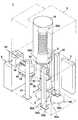
- a CVD apparatus 1includes a housing body 2 of substantially a hexahedral box shape having a rectangle cross sectional shape.
- Two clean units 3are of a same height installed horizontally on the left side wall of the housing body 2 .
- the clean units 3provide clean air toward their corresponding retreat stages, respectively.
- a heat treatment stage 4is set around a center portion in the housing body 2 .
- a first retreat stage 5 and a second retreat stage 5 Aare set at a front left side and a rear left side of the heat treatment stage 4 , respectively.
- a wafer loading stage 7is set at a right front corner of the housing body 2 .
- a pod stage 8is set in front of the wafer loading stage 7 .
- a notch arrangement unit 9to arrange a notch (not shown) of a wafer is located at a left front corner of the housing body 2 .
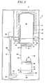
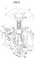
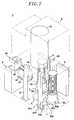
- a process tube 11 formed as a single body made of, e.g., quartzis vertically installed at an upper part of the heat treatment stage 4 , the process tube 11 having a shape of cylinder whose lower part being opened.
- the hollow part of the process tube 11forms a processing room 12 into which a plurality of wafers concentrically arranged in a boat are loaded.
- the bottom opening of the process tube 11serves as a throat 13 for loading and unloading wafers therethrough.
- the lower part of the process tube 11is coupled with an upper part of a manifold 14 through a seal ring 15 therebetween.
- the manifold 14is supported by the housing body 2 .
- the process tube 11is vertically supported.
- Installed through the side wall of the manifold 14 as illustrated in FIG. 2are an exhaust pipe 16 for evacuating the processing room 12 at a desired vacuum level and a gas inlet line 17 for supplying a source gas or a nitrogen gas into the processing room 12 .
- a heater unit 18 for heating the processing room 12is concentrically installed around the process tube 11 .
- the heater unit 18is vertically supported by the housing body 2 .
- a first boat elevator 20 to transfer a first boat 30 between the heat treatment state 4 and the first retreat stage 5is installed at a back position between the heat treatment stage 4 and the first retreat stage 5 .
- a second boat elevator 20 Ais installed next to the heat treatment stage 4 and the second retreat stage 5 A to transfer the second boat 30 A between the heat treatment state 4 and the second retreat stage 5 A.
- first and second boat elevators 20 and 20 Aare located at both sides of a line passing through the heat treatment stage 4 (a center of the process tube 11 ) and the wafer loading stage 7 (a wafer transfer unit 40 which is described later).
- the first and second boat elevators 20 and 20 Atransfer corresponding boats toward the wafer loading stage 7 and toward the opposite side of the wafer loading stage 7 , respectively.
- a center position of the process tube 11is disposed inside a triangle formed by connecting the wafer loading stage 7 , the boat elevator 20 and the boat elevator 20 A. Center positions of the first boat 30 and the second boat 30 A are located at one side (left side in this embodiment) of a straight line passing through the wafer loading stage 7 and the center position of the process tube 11 .
- first and the second boat elevators 20 , 20 A and the first and the second boats 30 , 30 Aare identically structured and function similarly, only the first boat elevator 20 and the first boat 30 will be described in detail with reference to FIGS. 2 and 3.
- the first boat elevator 20is installed at a predetermined position in the housing body 2 .
- the first boat elevator 20has a rotatably supported transfer screw shaft 21 which can be rotated in clockwise and counterclockwise directions by an electric motor 22 .
- An elevator support 23is screw-coupled with the transfer screw shaft 21 , thereby enabling the elevator support 23 to move up and down by the revolution of the transfer screw shaft 21 .
- a rotary actuator 24is horizontally mounted on the elevator support 23 .
- a cap 26is fixedly mounted in horizontal direction on the arm 25 to support the vertically installed first boat 30 .
- a fixing part 27is prepared on the cap 26 to fix the first boat 30 .
- the fixing part 27serves to fix the first boat 30 but is confined to be able to release the first boat 30 for maintenance, e.g., cleaning of the first boat 30 .
- the first boat 30has an upper end plate 31 , a lower end plate 32 and a plurality of, e.g., three, supporting members 33 vertically arranged between the upper end plate 31 and the lower end plate 32 .
- Each of the supporting members 33is provided with a multiplicity of, e.g., 100 to 200, vertically spaced wafer holding slots 34 for receiving and holding wafers W.
- a set of the slots at a same level of the three supporting membersserves to hold one wafer.
- a heat insulating cap 35 having a cylindrical shapeis installed under the lower end plate 32 of the first boat 30 , wherein a base 36 of a disc shape is extruded under the bottom of the heat insulating cap 35 .
- the base 36is faced with the top surface of the cap 26 of the first boat elevator 20 and fixed by the fixing part 27 .
- the wafer transfer unit 40carries the wafers W among the pod stage 8 , the notch arrangement unit 9 and the heat treatment stage 4 .
- the wafer transfer unit 40transfers the wafers W between a pod 50 , the notch arrangement unit 9 and the boats 30 and 30 A.
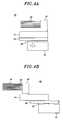
- the wafer transfer unit 40includes a base 41 , a rotary actuator 42 horizontally mounted on the base 41 , a first linear actuator 43 mounted on the rotary actuator 42 .
- a second linear actuator 44is horizontally mounted on the first linear actuator 43 and an installation unit 45 mounted on the second linear actuator 44 .
- the rotary actuator 42serves to rotate the first linear actuator 43 on a horizontal plane.
- the first linear actuator 43can linearly reciprocate the second linear actuator 44 .
- the second linear actuator 44can linearly reciprocate the installation unit 45 .
- a plurality of horizontally elongated tweezers 46e.g., five tweezers in FIGS. 4A and 4B
- the wafer transfer unit 40moves up and down by an elevator 47 having a transfer screw mechanism.
- each pod stage 8Mounted on each pod stage 8 is one front opening unified pod (FOUP) 50 serving as a carrier unit (accommodation unit) to carry wafers W.
- FOUPfront opening unified pod
- the pod 50has a hexahedral box like shape with an opening at one face thereof.
- a door 51is detachably mounted on the opening of the pod.
- the wafersWith the use of a pod as a carrier of wafers, the wafers can be kept protected from contaminations in ambient atmosphere while being transferred since the pod containing wafers are airtightly closed. As a result, the degree of cleanliness required for a clean room accommodating a CVD apparatus therein may be lowered, thereby reducing cost for the maintenance of the clean room.
- the pod 50is used as a carrier of the wafers. Further, there is installed at the pod stage 8 a pod opener (not shown) for opening the pod 50 by detaching the door 51 off the pod 50 .
- the first boat 30 supported by the first boat elevator 20is retired in the first retreat stage 5 while the second boat 30 A supported by the second boat elevator 20 A is loaded into and processed in the processing room 12 of the process tube 11 .
- a cap 26 A supporting the second boat 30 Ais descended by the second boat elevator 20 A, thereby unloading the second boat 30 A from the processing room 12 of the process tube 11 .
- the throat 13is closed by a shutter (not shown) to prevent the high temperature condition inside the processing room 12 from being destroyed.
- the second boat 30 A unloaded from the processing room 12(from now on referred to as also a processed boat 30 A) and the wafers therein are at a high temperature state.
- the high temperature processed boat 30 A unloaded from the processing room 12is removed from the heat treatment stage 4 located at the axial line of the process tube 11 to the second retreat stage 5 A by a rotary actuator 24 A of the second boat elevator 20 A. Since the second retreat stage 5 A is located around an outlet of the clean unit 3 outputting clean air, the high temperature processed boat 30 A placed at the second retreat stage 5 A is effectively cooled down by the clean air outputted from the clean unit 3 .
- the empty first boat 30 without carrying any wafer thereinis transferred from the first retreat stage 5 to the heat treatment stage 4 by the rotary actuator 24 of the first boat elevator 20 .
- the wafers W in the pod 50are transferred to the first boat 30 by the wafer transfer unit 40 . Since the processed boat 30 A placed at the second retreat stage 5 A can be sufficiently cooled down by the clean unit 3 before wafer transfer process starts, the wafers being transferred may not be thermally affected by the processed boat 30 A located at the heat treatment stage 4 .
- the pod 50 provided on the pod stage 8is opened by opening the door 51 through a release operation of a pod opener (not shown). After the pod 50 is opened, the wafer transfer unit 40 transfers the wafers W from the pod 50 to the first boat 30 via the notch arrangement unit 9 .
- the second linear actuator 44 and the installation unit 45are moved toward the pod 50 .
- the tweezers 46are inserted into the pod 50 to pick up the wafers W in the pod 50 therewith.
- the second linear actuator 44 and the installation unit 45are retracted to a position as shown in FIG. 4 A.
- the rotary actuator 42rotates about 90° and the second linear actuator 44 and the installation unit 45 are moved toward the notch arrangement unit 9 .
- the wafers W on the tweezers 46are loaded into the notch arrangement unit 9 by the operation of the elevator 47 .
- the wafer transfer unit 40picks up the wafers W from the notch arrangement unit 9 by employing the tweezers 46 and then retracts the tweezers 46 to the location shown in FIG. 4 A.
- the rotary actuator 42is rotated about 90° and the second linear actuator 44 and the installation unit 45 are extended toward the heat treatment stage 4 .
- the wafers W on the tweezers 46are transferred into the wafer holding slots 34 of the boat 30 .
- the wafer transfer unit 40retreats the second linear actuator 44 and the installation unit 45 and rotates the rotary actuator 42 by about 180°.
- the tweezers 46are arranged to face toward the pod 50 as the state shown in FIG. 4 A.
- the wafer transfer unit 40can transfer five wafers W at a time from the five slots of the pod 50 to the five wafer holding slots 34 of the boat 30 .
- the wafer transfer unit 40mounts a preset number of wafers W from a plurality of pods 50 to be transferred to one boat by the operation of the elevator 47 . If the wafers in the pod 50 are notch-arranged, the wafer transfer unit 40 transfers the wafers W from the pod 50 to the boat 30 without passing through the notch arrangement unit 9 .
- the first boat 30After the preset number of wafers W are mounted on the first boat 30 , the first boat 30 is lifted and loaded into the processing room 12 of the process tube 11 by the elevator 20 as illustrated in FIG. 3 . When the first boat 30 moves up to an upper limit, the periphery portion of the upper surface of the cap 26 and the bottom surface of the manifold 14 are tightly coupled with the seal ring 15 intervening therebetween, thereby air-tightly sealing the processing room 12 .
- the processing room 12Under a condition that the processing room 12 is airtightly closed by the cap 26 , the processing room 12 is evacuated to achieve a predetermined vacuum level. Then the processing room 12 is heated to a predetermined processing temperature (e.g., 800° C. to 1000° C.) and a processing gas of a preset flow rate is fed into the processing room 12 through the gas inlet line 17 . As a result, a CVD film is formed on each wafer W by the CVD reaction.
- a predetermined processing temperaturee.g. 800° C. to 1000° C.
- the processed boat 30 A located at the second retreat stage 5 Ais transferred to the heat treatment stage 4 by the rotary actuator 24 A of the second boat elevator 20 A while the first boat 30 is processed in the processing room 12 of the process tube 11 .
- the processed boat 30 Ais fully cooled down so that it is maintained at a temperature lower than, e.g., about 150° C.
- Three supporting members 33 of the processed boat 30 A transferred in the heat treatment stage 4are kept open towards the wafer transfer unit 40 as shown in FIG. 1 .
- the wafer transfer unit 40takes the wafers W from the processed boat 30 A at the heat treatment stage 4 to transfer them to the empty pod 50 of the pod stage 8 .
- the wafer transfer unit 40transfers the wafers W from the processed boat 30 A to plural pods on the pod stage 8 .
- the pod holding the loaded wafersis released from the pod stage 8 and then transferred to another place.
- the empty second boat 30 Ais transferred to the second retreat stage 5 A by the second boat elevator 20 A and remains thereat until a next operation begins.
- the cap 26 supporting the first boat 30is lowered down by the first boat elevator 20 .
- the first boat 30is unloaded from the processing room 12 of the process tube 11 .
- the throat 13 thereofis closed by the shutter (not shown) to sustain the high temperature condition of the processing room 12 .
- the first boat 30 unloaded from the processing room 12 and wafers W accommodated by the first boat 30are at a high temperature state.
- the processed first boat 30 being at a high temperature and unloaded from the processing room 12is transferred from the heat treatment stage 4 toward the first retreat stage 5 by the rotary actuator 24 of the first boat elevator 20 . Since the first retreat stage is positioned close to the outlet of the clean unit 3 outputting clean air, the processed first boat 30 transferred to the first retreat stage 5 can be effectively cooled down by the clean air outputted from the clean unit 3 .
- wafers Ware batch-processed by the CVD apparatus 1 by repeating the process described above.
- wafers to be processedare loaded in an empty boat after transferring the processed boat to the retreat stage.
- wafers to be processedmay be transferred to a boat while other wafers are being processed in the process tube if the film to be deposited is not thermally sensitive.
- each of two boatsis configured to move between the heat treatment stage and the retreat stage by employing a rotary actuator mounted on an elevator support unit of the corresponding boat elevator, two boats can move independently by using simply structured boat elevators, thereby reducing a manufacturing cost of the CVD apparatus.
- a boatSince a boat is fixedly mounted on the cap supported by an arm of a corresponding boat elevator, a boat can be protected from tripping or falling down, e.g., due to an earthquake and therefore it becomes possible to prevent the damage generation of wafers or boats.
- the wafer transfer unit 40 and the boat elevators 20 , 20 Aare configured to be located close to the heat treatment stage 4 in a manner of surrounding the heat treatment stage 4 in FIG. 1 and exchange operation of the processed boat with the empty boat is carried out between the first and second retreat stages and heat treatment stage. Accordingly, a radius of rotation of each arm of the first and second boat elevators can be decreased, enabling to reduce the footprint of the CVD apparatus by diminishing the (left/right and front/back) dimension of the housing body of the CVD apparatus.
- COOCost of ownership
- the wafer transfer unitcan transfer wafers accommodated in any of the boats at the heat treatment stage which is a boat loading and unloading position under the process tube, wafers can be transferred with respect to any of the first and the second boats at one heat treatment stage. This results in saving of a moving area of the substrate transfer unit to thereby decrease the footprint thereof.
- the first boat elevatorcan move the first boat toward the wafer transfer unit and the second boat elevator can move the second boat toward the opposite side of the wafer transfer unit. This results in further decreasing of the footprint thereof.
- the wafer transfer unitcan transfer wafers accommodated in any of the first and second boats at the boat loading/unloading position under the process tube, wafers can be transferred with respect to any of the first and second boats at one heat treatment stage. This results in saving of a moving area of the wafer transfer unit apparatus to thereby decrease the footprint thereof.
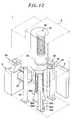
- FIGS. 9 to 12outline schematic views for describing a CVD apparatus managing method in accordance with a second preferred embodiment of the present invention.
- the second CVD apparatus managing methodis different from the first CVD apparatus managing method in that while one boat is being processed, unprocessed wafers are loaded on the other boat and then the other boat is transferred to a location above the retreat stage, thereby further suppressing the thermal influence from the processed boat to the unprocessed wafers.
- the processed first boat 30is lowered by the first boat elevator 20 .
- the second boat 30 A accommodating the new wafers W at the upper position of the second retreat stage 5 Ais farther away from the heat treatment stage 4 , the new wafers W accommodated in the second boat 30 A is prevented from being affected by the thermal influence from the processed first boat 30 .
- the processed first boat 30is moved to an upper location of the first retreat stage 5 and the second boat 30 A accommodating new wafers is loaded into the process tube 11 .
- the processed first boat 30is returned to the heat treatment stage 4 and the processed wafers are unloaded from the first boat 30 ; and new wafers to be processed are mounted on the first boat 30 supported by the first boat elevator 20 .
- the first boat 30 accommodating the new wafersare transferred from the heat treatment stage 4 to the first retreat stage 5 by the rotary actuator 24 and then moved to the upper position of the first retreat stage 5 by the first boat elevator 20 as shown in FIG. 11 .
- the processed second boat 30 Ais descended by the second boat elevator 20 A.
- the first boat 30 accommodating the new wafers Wis moved at the upper position of the first retreat stage 5 , which is farther away from the heat treatment stage 4 , the new wafers W accommodated in the first boat 30 can be protected from the thermal influence from the processed second boat 30 A at high temperature.
- thermal influence from the processed boat to the new waferscan be further avoided in comparison with the first CVD apparatus managing method.
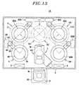
- FIG. 13presents a schematic top plan view of a CVD apparatus 1 A in accordance with a second preferred embodiment of the present invention.
- the CVD apparatus 1 A in accordance with the second preferred embodimentis different from the CVD apparatus 1 of the first preferred embodiment in that CVD apparatus 1 A in accordance with the second preferred embodiment has two process tubes (including heater units), four boats, four boat elevators and three retreat stages.
- the CVD apparatus 1 A in accordance with the second preferred embodimentwill be described in detail.
- the side of a pod stage 8will be referred to as the front side and its opposite side, as the backside.
- a first heat treatment stage 4 and a second heat treatment stage 4 Aare set symmetrically at backside of the housing body 2 as illustrated in FIG. 13, wherein a first process tube 11 and a second process tube 11 are installed at the first heat treatment stage 4 and the second heat treatment stage 4 A, respectively.
- a first boat elevator 20 to carry a first boat 30 and a second boat elevator 20 A to carry a second boat 30 Aare disposed diagonally with respect to the first heat treatment stage 4 .
- a third boat elevator 20 B to carry a third boat 30 B and a fourth boat elevator 20 C to carry a fourth boat 30 Care disposed diagonally with respect to the second heat treatment stage 4 A.
- the first retreat stage 5 where the first boat 30 retreatis located at the front side of the first heat treatment stage 4 ; the second retreat stage SA for the second boat 30 A, at the right hand side of the first heat treatment stage 4 .
- a third retreat stage 5 B for the third boat 30 Bis positioned at the front side of the second heat treatment stage 4 A; a fourth retreat stage 5 C for the fourth boat 30 C is disposed at the left hand side of the second heat treatment stage 4 A.
- the second retreat stage 5 A and the fourth retreat stage 5 Cshare the same space between the first heat treatment stage 4 and the second heat treatment stage 4 A.
- the CVD apparatus 1 Ais provided with one wafer loading stage 7 at a front center region of the housing body 2 .
- the wafer transfer unit 40 installed at the wafer loading stage 7transfers wafers W between the first and the second heat treatment stages 4 , 4 A and the pod stage 8 .
- the boat elevators 20 and 20 Aare located at opposite sides with respect to the line connecting the process tube 11 and the wafer transfer unit 40 ; and the boat elevators 20 B and 20 C are located at opposite sides with respect to the line connecting the process tube 11 A to the wafer transfer unit 40 .
- the first heat treatment stage 4is shared by the first and the second boat elevators 20 , 20 A and the second heat treatment stage 4 A is shared by the third and the fourth boat elevators 20 B, 20 C. Further, the second and the fourth boat elevators 20 A, 20 C share one retreat stage located between the first and the second heat treatment stages 4 , 4 A.
- the second boat 30 Ashould be at its retreat stage 5 A; the fourth boat 30 C is to be in the second process tube 11 ; and the third boat 30 B should be at its retreat stage 5 B.
- the fourth boat 30 Cshould be at its retreat stage 5 C; the second boat 30 A should be in the first process tube 11 ; and the first boat 30 should be at its retreat stage 5 .
- a CVD apparatus managing method of the CVD apparatus 1 A in accordance with the second preferred embodimentis the same as that of the CVD apparatus 1 in accordance with the first preferred embodiment.
- the CVD apparatus 1 A in accordance with the second preferred embodimentprovides, in addition to the advantageous effects obtainable by the CVD apparatus 1 in accordance with the first preferred embodiment, further advantageous effects as follows.
- CVD apparatus 1 Ain accordance with the second preferred embodiment employs two process tubes, four boat elevators and four boats, the throughput thereof can be enhanced.
- initial cost and running cost for managing the CVD apparatuscan be greatly reduced to thereby decrease the COO thereof.
- FIG. 14depicts a schematic plan view of a CVD apparatus 1 B in accordance with a third preferred embodiment of the present invention.
- FIG. 15shows a schematic sectional side view of the CVD apparatus 1 B.
- the CVD apparatus 1 B in accordance with the third preferred embodimentis different from the CVD apparatus 1 , 1 A in accordance with the first and the second preferred embodiments in that in the CVD apparatus 1 B, there is provided in the space of the housing body 2 under the process tube 11 with a load-lock chamber structure 60 accommodating the space occupied by the heat treatment stage 4 , the first and the second retreat stages 5 , 5 A and the first and the second boat elevators 22 , 20 A.
- the CVD apparatus 1 B in accordance with the third preferred embodimentwill be described focusing on the load-lock chamber structure 60 .
- a side of a pod stage 8 of FIG. 14is defined as a front side; its opposite side, as a backside; a side of a notch arrangement unit 9 , as a left side; and its opposite side as a right side.
- a load-lock chamber 61(from now on referred to as a chamber 61 ) constituting a sealing room 62 is provided at a backside of the housing 2 under the process tube 11 .
- the heat treatment stage 4is located at a front center region of the sealing room 62 .
- the first retreat stage 5is positioned at left backside of the heat treatment stage 4 .
- the second retreat stage 5 Ais located at right backside of the heat treatment stage 4 .
- the heat treatment stage 4is located close to the wafer transfer unit 40 but the retreat stages 5 , 5 A are located away from the wafer transfer unit 40 .
- a process tube 11is installed at a position of the ceiling wall of the chamber 61 above the heat treatment stage 4 in the chamber 61 , wherein the process tube 11 is connected to the sealing room 12 .
- the first boat elevator 20 to transfer the first boat 30is installed at left side of the heat treatment stage 4 and at front side of the first retreat stage 5 .
- the second boat elevator 20 A to transfer the second boat 30 Ais installed at right side of the heat treatment stage 4 and at front side of the second retreat stage 5 A.
- an inert gas supplying line 64 to supply inert gas 63 such as nitrogen gas into the sealing room 62is connected at the ceiling of the chamber 61 .
- An exhaust line 65 to exhaust gas from the sealing room 62is installed at the bottom wall of the chamber 61 .
- the sealing room 62 of the chamber 61is purged by the inert gas 63 .
- a wafer loading/unloading opening 66is installed on front wall of an upper part of the chamber 61 to connect the sealing room 62 to a front side room of the housing body 2 .
- a gate valve 67is installed at the wafer loading/unloading opening 66 to open and close the wafer loading/unloading opening 66 when needed.
- the wafer transfer unit 40installed on the loading stage 7 located in the front side room of the housing body 2 carries (charges or discharges) wafers W through the wafer loading/unloading opening 66 to the first boat 30 or the second boat 30 A transferred to the heat treatment stage 4 .
- a CVD apparatus managing method of the CVD apparatus 1 B of the third preferred embodimentis the same as the first or the second CVD apparatus managing method except that the chamber 61 is purged with an inert gas.
- the wafer loading/unloading opening 66is closed by the gate valve 67 and the sealing room 62 of the chamber 61 is purged by the inert gas 63 fed therein through the inert gas supply line 64 and evacuated therefrom through the exhaust line 65 .
- the wafer loading/unloading opening 66is opened by the gate valve 67 .
- the CVD apparatus 1 B in accordance with the third preferred embodimentprovides, as well as the advantageous effects obtainable by the CVD apparatus in accordance with the first and the second preferred embodiment, further advantages and effects as follows.
- the heat treatment stage, the first retreat stage and the second retreat stageconstitute a load-lock chamber which is purged by an inert gas, the wafers W are prevented from making contact with oxygen and moisture contained in air before and after the heat treatment thereof. Accordingly, unnecessary oxide film (natural oxide film) formation on the wafers W due to oxygen or moisture in the ambient air can be effectively prevented.
- the present inventionis not limited thereto and can be also equally applied to a heat treatment apparatus such as a batch-type vertical diffusion apparatus or other types of semiconductor manufacturing apparatus as well.
- the present inventioncan also be employed in processing other types of substrates including a photo mask, a printed circuit board, a liquid crystal panel, a compact disk, a magnetic disk and the like.
Landscapes
- Engineering & Computer Science (AREA)
- Chemical & Material Sciences (AREA)
- Manufacturing & Machinery (AREA)
- General Physics & Mathematics (AREA)
- Physics & Mathematics (AREA)
- Computer Hardware Design (AREA)
- Microelectronics & Electronic Packaging (AREA)
- Power Engineering (AREA)
- Condensed Matter Physics & Semiconductors (AREA)
- General Chemical & Material Sciences (AREA)
- Chemical Kinetics & Catalysis (AREA)
- Materials Engineering (AREA)
- Mechanical Engineering (AREA)
- Metallurgy (AREA)
- Organic Chemistry (AREA)
- Container, Conveyance, Adherence, Positioning, Of Wafer (AREA)
Abstract
Description
The present invention relates to a substrate processing apparatus; and, more particularly, to a substrate processing apparatus capable of suppressing oxidation and contamination of a substrate under processing.
In a semiconductor device manufacturing factory, there have been widely employed batch-type vertical hot-wall furnaces (from now on, referred to as furnaces) in a thermal process such as an annealing, an oxide film forming, a diffusion or a thin film forming process on a semiconductor wafer.
U.S. Pat. No. 4,770,590 discloses one of such furnaces. In this furnace, a boat exchanger is installed between a wafer transfer unit and the space just under a process tube and there are mounted a pair of boats on a turning table of the boat exchanger, wherein a processed boat is substituted with an unprocessed boat by turning the pair of boats by 180° on the turning table with respect to a boat elevator. Namely, in this furnace, while one boat (a first boat) accommodating a set of wafers is processed in the process tube, new wafers (unprocessed wafers) are mounted on the other boat (a second boat) and then transferred by a wafer transfer unit to thereby enhance a throughput thereof.
In this conventional furnace, however, impurities, e.g. contaminants, may be produced during the exchange operation of the boats. Further, since the boats are not fixedly mounted on the turning table, it may be possible that the boats may fall down during the exchange operation thereof or due to an external impact, e.g., an earthquake.
Further, Japanese Patent Laid Open Publication No. 9-289173 discloses a vertical hot-wall furnace including a first boat elevator for mounting and transferring a first boat having wafers mounted thereon between a wafer transfer region and a process tube and a first boat elevator for mounting and transferring a second boat having wafers mounted thereon between the wafer transfer region and the process tube, wherein a boat exchange operation is not executed with respect to a boat elevator such as one disclosed in the above-mentioned U.S. Pat. No. 4,770,590 to thereby enhance a throughput thereof.
Meanwhile, in the a vertical hot-wall furnace disclosed in the Japanese Patent Laid Open Publication No. 9-289173, since the boat exchange operation is not executed with respect to the boat elevator, there entails no position deviation problem and accordingly, the boat capsize problem is prevented. However, since a center position of a heat processing chamber is located on a straight line passing through a position of the first boat elevator and a position of the second boat elevator, a distance between the first boat elevator and the second boat elevator becomes about two times of each arm (rotating unit) of the boat elevators.
This requires an increase a horizontal width (opening) of the vertical hot-wall furnace to thereby increase a dimension thereof. Further, since wafers in the first and second boats transferred from the process tube to preset positions apart therefrom by the first and second boat elevators are carried by a wafer transfer unit, the carrying area of the wafer transfer unit becomes larger and accordingly, footprint (occupying area) thereof becomes large.
It is, therefore, an object of the present invention to provide a semiconductor manufacturing apparatus capable of preventing or reducing generation of impurities and avoiding the tripping or the falling down of boats.
Another object of the present invention is to provide a semiconductor manufacturing apparatus capable of preventing unprocessed boats from being affected by the heat generated from processed boats.
In accordance with a first preferred embodiment of the present invention, there is provided a substrate processing apparatus comprising: a process tube for processing a plurality of substrates; two boats for accommodating the substrates; two boat elevators, each having one boat mounted thereon, the boat elevators carrying the boats between a first position located below the process tube and two corresponding second positions and loading and unloading the boats into and from the process tube at the first position; and a substrate transfer unit for loading and unloading the substrates into and from the boats when the boats are at the first position, wherein a center position of the process tube is disposed inside a triangle formed by connecting the substrate transfer unit and the two boat elevators.
In accordance with the first embodiment, since a center position of the process tube is disposed inside a triangle formed by connecting the substrate transfer unit and the two boat elevators, the space between the two boat elevators can be saved to thereby decrease a horizontal width of the substrate processing apparatus. Further, since the substrate transfer unit can transfer wafers accommodated in any of the two boats at the first position, wafers can be transferred with respect to any of the two boats at one heat treatment stage. This results in saving of a moving area of the substrate transfer unit to thereby decrease the footprint thereof.
In accordance with a second preferred embodiment of the present invention, there is provided a substrate processing apparatus comprising: a substrate processing apparatus comprising: a process tube for processing a plurality of substrates; two boats for accommodating the substrates; two boat elevators for carrying the boats between a first position located below the process tube and two corresponding second positions and loading and unloading the boats into and from the process tube at the first position; and a substrate transfer unit for loading and unloading the substrates into and from the boats, wherein the boat elevators are located at both sides of a line passing through a center of the process tube and the substrate transfer unit and one of the boats is moved by its corresponding boat elevator toward the substrate transfer unit from the first position and the other boat is moved by its corresponding boat elevator toward the opposite side of the substrate transfer unit from the first position.
In the second embodiment, the boat elevators are located at both sides of a line passing through a center of the process tube and the substrate transfer unit and one of the boats is moved by its corresponding boat elevator toward the substrate transfer unit from the first position and the other boat is moved by its corresponding boat elevator toward the opposite side of the substrate transfer unit from the first position. As a result, a horizontal width and a footprint of the substrate processing apparatus can be saved.
In accordance with the first and second embodiments, since the boat elevator can transfer the boats between the first position located below the process tube and the two corresponding second positions, the boat fixedly mounted on the boat elevator can be loaded and unloaded into and from the process tube. Accordingly, the generation of impurity particles can be avoided when a processed boat and an unprocessed boat are exchanged. Further, a capsize problem can be overcome during the exchange operation or an earthquake generation.
In accordance with a third preferred embodiment of the present invention, there is provided a substrate processing apparatus comprising: two process tubes for processing a plurality of substrates; four boats for accommodating the substrates; four boat elevators, each boat elevator for loading and unloading one of the boats into and from one of the process tubes and carrying said one of the boats between one of two first positions below the process tubes and one of three corresponding second positions; and a substrate transfer unit for loading and unloading the substrates into and from the boats.
The above and other objects and features of the present invention will become apparent from the following description of preferred embodiments given in conjunction with the accompanying drawings in which:
FIG. 1 shows a schematic plan view of a chemical vapor deposition (CVD) apparatus in accordance with a first preferred embodiment of the present invention;
FIG. 2 depicts a vertical cross sectional view of the CVD apparatus taken along a line II—II as shown in FIG. 1;
FIG. 3 provides a vertical cross sectional view of the CVD apparatus during a wafer processing therein in accordance with the first preferred embodiment;
FIGS. 4A and 4B present side views of a wafer transfer unit during a shortened state and an elongated state thereof,5respectively;
FIG. 5 illustrates a schematic view of the CVD apparatus during processing of a second boat in accordance with the first preferred embodiment of the present invention, which is used in describing a first CVD apparatus managing method;
FIG. 6 sets forth a schematic view of the CVD apparatus after unloading the second boat;
FIG. 7 represents a schematic view of the CVD apparatus after retreat of the second boat;
FIG. 8 exemplifies a schematic view of the CVD apparatus during a wafer transferring process by employing a first boat in accordance with the first CVD apparatus managing method;
FIG. 9 outlines a schematic view of the CVD apparatus while retreating the second boat to a preset position above a wafer loading/unloading position which is used in describing a second CVD apparatus managing method;
FIG. 10 gives a schematic view of the CVD apparatus after unloading of the first boat;
FIG. 11 represents a schematic view of the CVD apparatus while retreating the first boat to a preset position above a wafer loading/unloading position;
FIG. 12 sets forth a schematic view of the CVD apparatus after unloading the second boat in accordance with the second CVD apparatus managing method;
FIG. 13 presents a schematic plan view of a CVD apparatus in accordance with a second preferred embodiment of the present invention;
FIG. 14 depicts a schematic plan view of a CVD apparatus in accordance with a third preferred embodiment of the present invention; and
FIG. 15 shows a schematic sectional side view of the CVD apparatus in accordance with the third preferred embodiment of the present invention.
Preferred embodiments of the present invention will now be described with reference to FIGS. 1-15. A semiconductor manufacturing apparatus in accordance with a preferred embodiment of the present invention is a batch-type vertical hot-wall furnace (from now on, referred to as a furnace), e.g., a chemical vapor deposition (CVD) apparatus, which is employed in depositing a CVD film on an wafer serving as a substrate. In the following description for the preferred embodiments, front and back, left and right sides are defined with reference to FIG.1. Namely, the lower side where apod stage 8 is located is referred to as a front side and its opposite side is referred to as a backside. The left-hand side where aclean unit 3 is disposed is referred to as a left side and its opposite side is referred to as a right side.
As shown in FIG. 1, aCVD apparatus 1 includes ahousing body 2 of substantially a hexahedral box shape having a rectangle cross sectional shape. Twoclean units 3 are of a same height installed horizontally on the left side wall of thehousing body 2. Theclean units 3 provide clean air toward their corresponding retreat stages, respectively.
Aheat treatment stage 4 is set around a center portion in thehousing body 2. Afirst retreat stage 5 and asecond retreat stage 5A are set at a front left side and a rear left side of theheat treatment stage 4, respectively.
Awafer loading stage 7 is set at a right front corner of thehousing body 2. Apod stage 8 is set in front of thewafer loading stage 7. Anotch arrangement unit 9 to arrange a notch (not shown) of a wafer is located at a left front corner of thehousing body 2. From now on, structures of the above stages will be described in detail.
As illustrated in FIGS. 2 and 3, aprocess tube 11 formed as a single body made of, e.g., quartz is vertically installed at an upper part of theheat treatment stage 4, theprocess tube 11 having a shape of cylinder whose lower part being opened. The hollow part of theprocess tube 11 forms aprocessing room 12 into which a plurality of wafers concentrically arranged in a boat are loaded. The bottom opening of theprocess tube 11 serves as athroat 13 for loading and unloading wafers therethrough.
The lower part of theprocess tube 11 is coupled with an upper part of a manifold14 through aseal ring 15 therebetween. The manifold14 is supported by thehousing body 2. As a result, theprocess tube 11 is vertically supported. Installed through the side wall of the manifold14 as illustrated in FIG. 2 are anexhaust pipe 16 for evacuating theprocessing room 12 at a desired vacuum level and agas inlet line 17 for supplying a source gas or a nitrogen gas into theprocessing room 12. Outside theprocess tube 11, aheater unit 18 for heating theprocessing room 12 is concentrically installed around theprocess tube 11. Theheater unit 18 is vertically supported by thehousing body 2.
Afirst boat elevator 20 to transfer afirst boat 30 between theheat treatment state 4 and thefirst retreat stage 5 is installed at a back position between theheat treatment stage 4 and thefirst retreat stage 5. Asecond boat elevator 20A is installed next to theheat treatment stage 4 and thesecond retreat stage 5A to transfer thesecond boat 30A between theheat treatment state 4 and thesecond retreat stage 5A.
In detail, the first andsecond boat elevators wafer transfer unit 40 which is described later). The first andsecond boat elevators wafer loading stage 7 and toward the opposite side of thewafer loading stage 7, respectively.
Further, a center position of theprocess tube 11 is disposed inside a triangle formed by connecting thewafer loading stage 7, theboat elevator 20 and theboat elevator 20A. Center positions of thefirst boat 30 and thesecond boat 30A are located at one side (left side in this embodiment) of a straight line passing through thewafer loading stage 7 and the center position of theprocess tube 11.
Since the first and thesecond boat elevators second boats first boat elevator 20 and thefirst boat 30 will be described in detail with reference to FIGS. 2 and 3.
As shown in FIGS. 2 and 3, thefirst boat elevator 20 is installed at a predetermined position in thehousing body 2. Thefirst boat elevator 20 has a rotatably supportedtransfer screw shaft 21 which can be rotated in clockwise and counterclockwise directions by anelectric motor 22. Anelevator support 23 is screw-coupled with thetransfer screw shaft 21, thereby enabling theelevator support 23 to move up and down by the revolution of thetransfer screw shaft 21. Arotary actuator 24 is horizontally mounted on theelevator support 23. Acap 26 is fixedly mounted in horizontal direction on thearm 25 to support the vertically installedfirst boat 30. A fixingpart 27 is prepared on thecap 26 to fix thefirst boat 30. The fixingpart 27 serves to fix thefirst boat 30 but is confined to be able to release thefirst boat 30 for maintenance, e.g., cleaning of thefirst boat 30.
As illustrated in FIGS. 2 and 3, thefirst boat 30 has anupper end plate 31, alower end plate 32 and a plurality of, e.g., three, supportingmembers 33 vertically arranged between theupper end plate 31 and thelower end plate 32. Each of the supportingmembers 33 is provided with a multiplicity of, e.g., 100 to 200, vertically spacedwafer holding slots 34 for receiving and holding wafers W. A set of the slots at a same level of the three supporting members serves to hold one wafer.
Periphery portions of the wafers W are inserted in the corresponding supporting slots to thereby render the wafers W to be arranged horizontally and their center lines to be maintained on a same vertical line. Aheat insulating cap 35 having a cylindrical shape is installed under thelower end plate 32 of thefirst boat 30, wherein abase 36 of a disc shape is extruded under the bottom of theheat insulating cap 35. Thebase 36 is faced with the top surface of thecap 26 of thefirst boat elevator 20 and fixed by the fixingpart 27.
Returning to FIG. 1, there is installed awafer itransfer unit 40 in thewafer loading stage 7. Thewafer transfer unit 40 carries the wafers W among thepod stage 8, thenotch arrangement unit 9 and theheat treatment stage 4. In other words, thewafer transfer unit 40 transfers the wafers W between apod 50, thenotch arrangement unit 9 and theboats
As shown in FIGS. 4A and 4B, thewafer transfer unit 40 includes abase 41, arotary actuator 42 horizontally mounted on thebase 41, a firstlinear actuator 43 mounted on therotary actuator 42. A secondlinear actuator 44 is horizontally mounted on the firstlinear actuator 43 and aninstallation unit 45 mounted on the secondlinear actuator 44.
Therotary actuator 42 serves to rotate the firstlinear actuator 43 on a horizontal plane. The firstlinear actuator 43 can linearly reciprocate the secondlinear actuator 44. The secondlinear actuator 44 can linearly reciprocate theinstallation unit 45. A plurality of horizontally elongated tweezers46 (e.g., five tweezers in FIGS. 4A and 4B) with a constant vertical gap therebetween are mounted onto a side-wall of theinstallation unit 45. Thewafer transfer unit 40 moves up and down by anelevator 47 having a transfer screw mechanism.
Mounted on eachpod stage 8 is one front opening unified pod (FOUP)50 serving as a carrier unit (accommodation unit) to carry wafers W. Even though only onepod stage 8 is illustrated in FIGS. 1 and 5 for the sake of simplicity, it should be apparent to those who skilled in the art that more than one pod stage can be provided on theCVD apparatus 1. Thepod 50 has a hexahedral box like shape with an opening at one face thereof. Adoor 51 is detachably mounted on the opening of the pod.
With the use of a pod as a carrier of wafers, the wafers can be kept protected from contaminations in ambient atmosphere while being transferred since the pod containing wafers are airtightly closed. As a result, the degree of cleanliness required for a clean room accommodating a CVD apparatus therein may be lowered, thereby reducing cost for the maintenance of the clean room.
Accordingly, in theCVD apparatus 1 in accordance with the preferred embodiment of the present invention, thepod 50 is used as a carrier of the wafers. Further, there is installed at the pod stage8 a pod opener (not shown) for opening thepod 50 by detaching thedoor 51 off thepod 50.
The operation of the CVD apparatus in accordance with a preferred embodiment of the present invention will now be described with reference to FIGS. 5 to8.
As depicted in FIG. 5, thefirst boat 30 supported by thefirst boat elevator 20 is retired in thefirst retreat stage 5 while thesecond boat 30A supported by thesecond boat elevator 20A is loaded into and processed in theprocessing room 12 of theprocess tube 11.
After a desired processing is completed, as illustrated in FIG. 6, acap 26A supporting thesecond boat 30A is descended by thesecond boat elevator 20A, thereby unloading thesecond boat 30A from theprocessing room 12 of theprocess tube 11. After thesecond boat 30A is unloaded, thethroat 13 is closed by a shutter (not shown) to prevent the high temperature condition inside theprocessing room 12 from being destroyed. Thesecond boat 30A unloaded from the processing room12 (from now on referred to as also a processedboat 30A) and the wafers therein are at a high temperature state.
As represented in FIG. 7, the high temperature processedboat 30A unloaded from theprocessing room 12 is removed from theheat treatment stage 4 located at the axial line of theprocess tube 11 to thesecond retreat stage 5A by arotary actuator 24A of thesecond boat elevator 20A. Since thesecond retreat stage 5A is located around an outlet of theclean unit 3 outputting clean air, the high temperature processedboat 30A placed at thesecond retreat stage 5A is effectively cooled down by the clean air outputted from theclean unit 3.
When the processedboat 30A is transferred to thesecond retreat stage 5A by thesecond boat elevator 20A, the emptyfirst boat 30 without carrying any wafer therein is transferred from thefirst retreat stage 5 to theheat treatment stage 4 by therotary actuator 24 of thefirst boat elevator 20. After the emptyfirst boat 30 is transferred to theheat treatment stage 4, the wafers W in thepod 50 are transferred to thefirst boat 30 by thewafer transfer unit 40. Since the processedboat 30A placed at thesecond retreat stage 5A can be sufficiently cooled down by theclean unit 3 before wafer transfer process starts, the wafers being transferred may not be thermally affected by the processedboat 30A located at theheat treatment stage 4.
As presented in FIG. 8, when the wafers W are transferred to the boat by thewafer transfer unit 40, thepod 50 provided on thepod stage 8 is opened by opening thedoor 51 through a release operation of a pod opener (not shown). After thepod 50 is opened, thewafer transfer unit 40 transfers the wafers W from thepod 50 to thefirst boat 30 via thenotch arrangement unit 9.
That is, as can be seen from FIGS. 4A and 4B, the secondlinear actuator 44 and theinstallation unit 45 are moved toward thepod 50. Then thetweezers 46 are inserted into thepod 50 to pick up the wafers W in thepod 50 therewith. Thereafter, the secondlinear actuator 44 and theinstallation unit 45 are retracted to a position as shown in FIG.4A. Subsequently, therotary actuator 42 rotates about 90° and the secondlinear actuator 44 and theinstallation unit 45 are moved toward thenotch arrangement unit 9. Then, the wafers W on thetweezers 46 are loaded into thenotch arrangement unit 9 by the operation of theelevator 47.
After the notch arrangement of the wafers W is completed at thenotch arrangement unit 9, thewafer transfer unit 40 picks up the wafers W from thenotch arrangement unit 9 by employing thetweezers 46 and then retracts thetweezers 46 to the location shown in FIG.4A.
Thereafter, therotary actuator 42 is rotated about 90° and the secondlinear actuator 44 and theinstallation unit 45 are extended toward theheat treatment stage 4. Then, the wafers W on thetweezers 46 are transferred into thewafer holding slots 34 of theboat 30. Thereafter, thewafer transfer unit 40 retreats the secondlinear actuator 44 and theinstallation unit 45 and rotates therotary actuator 42 by about 180°. Then, thetweezers 46 are arranged to face toward thepod 50 as the state shown in FIG.4A.
Since thewafer transfer unit 40 has fivetweezers 46, thewafer transfer unit 40 can transfer five wafers W at a time from the five slots of thepod 50 to the fivewafer holding slots 34 of theboat 30. In this case, since the number (e.g., 100 to 200) of wafers processed in batch on theboat 30 is greater than that (e.g., 25) accommodated in onepod 50, thewafer transfer unit 40 mounts a preset number of wafers W from a plurality ofpods 50 to be transferred to one boat by the operation of theelevator 47. If the wafers in thepod 50 are notch-arranged, thewafer transfer unit 40 transfers the wafers W from thepod 50 to theboat 30 without passing through thenotch arrangement unit 9.
After the preset number of wafers W are mounted on thefirst boat 30, thefirst boat 30 is lifted and loaded into theprocessing room 12 of theprocess tube 11 by theelevator 20 as illustrated in FIG.3. When thefirst boat 30 moves up to an upper limit, the periphery portion of the upper surface of thecap 26 and the bottom surface of the manifold14 are tightly coupled with theseal ring 15 intervening therebetween, thereby air-tightly sealing theprocessing room 12.
Under a condition that theprocessing room 12 is airtightly closed by thecap 26, theprocessing room 12 is evacuated to achieve a predetermined vacuum level. Then theprocessing room 12 is heated to a predetermined processing temperature (e.g., 800° C. to 1000° C.) and a processing gas of a preset flow rate is fed into theprocessing room 12 through thegas inlet line 17. As a result, a CVD film is formed on each wafer W by the CVD reaction.
The processedboat 30A located at thesecond retreat stage 5A is transferred to theheat treatment stage 4 by therotary actuator 24A of thesecond boat elevator 20A while thefirst boat 30 is processed in theprocessing room 12 of theprocess tube 11. At this time, the processedboat 30A is fully cooled down so that it is maintained at a temperature lower than, e.g., about 150° C.Three supporting members 33 of the processedboat 30A transferred in theheat treatment stage 4 are kept open towards thewafer transfer unit 40 as shown in FIG.1.
After the processedboat 30A is transferred to theheat treatment stage 4 by thesecond boat elevator 20A, thewafer transfer unit 40 takes the wafers W from the processedboat 30A at theheat treatment stage 4 to transfer them to theempty pod 50 of thepod stage 8. In this case, since the number of the wafers W processed in a batch of the processedboat 30A is greater than that which can be accommodated in onepod 50, thewafer transfer unit 40 transfers the wafers W from the processedboat 30A to plural pods on thepod stage 8. When a preset number of wafers W are transferred to oneempty pod 50, the pod holding the loaded wafers is released from thepod stage 8 and then transferred to another place.
After all the processed wafers W are transferred from the processedboat 30A to thepods 50, the emptysecond boat 30A is transferred to thesecond retreat stage 5A by thesecond boat elevator 20A and remains thereat until a next operation begins.
Meanwhile, when a predetermined time for thefirst boat 30 lapses, thecap 26 supporting thefirst boat 30 is lowered down by thefirst boat elevator 20. As a result, thefirst boat 30 is unloaded from theprocessing room 12 of theprocess tube 11. Thereafter, thethroat 13 thereof is closed by the shutter (not shown) to sustain the high temperature condition of theprocessing room 12. Thefirst boat 30 unloaded from theprocessing room 12 and wafers W accommodated by thefirst boat 30 are at a high temperature state.
As described above with respect to thesecond boat 30A, the processedfirst boat 30 being at a high temperature and unloaded from theprocessing room 12 is transferred from theheat treatment stage 4 toward thefirst retreat stage 5 by therotary actuator 24 of thefirst boat elevator 20. Since the first retreat stage is positioned close to the outlet of theclean unit 3 outputting clean air, the processedfirst boat 30 transferred to thefirst retreat stage 5 can be effectively cooled down by the clean air outputted from theclean unit 3.
The wafers W are batch-processed by theCVD apparatus 1 by repeating the process described above. In the preferred embodiment of the present invention described above, wafers to be processed are loaded in an empty boat after transferring the processed boat to the retreat stage. However, wafers to be processed may be transferred to a boat while other wafers are being processed in the process tube if the film to be deposited is not thermally sensitive.
The advantages and effects in accordance with the above-mentioned preferred embodiment of the present invention are as follows.
(1) Since two boats are employed, a film growing process for wafers in one boat and a wafer transferring process for the other boat can be accomplished simultaneously, thereby enhancing throughput of the CVD apparatus.
(2) Since the alternate use of two boats in processing wafers in the process tube is accomplished by configuring each of the two boat elevators to load and unload one boat into and from the process tube by moving between the heat treatment stage and the retreat stage, a boat need not be detached from a corresponding boat elevator and therefore can be fixedly mounted thereon. As a result, alternate operation of the two boats can be executed continuously without suffering from a misalignment of the wafers and particulate generation problem due to the movement of the boats against the boat elevators.
(3) Since each of two boats is configured to move between the heat treatment stage and the retreat stage by employing a rotary actuator mounted on an elevator support unit of the corresponding boat elevator, two boats can move independently by using simply structured boat elevators, thereby reducing a manufacturing cost of the CVD apparatus.
(4) Since a boat is fixedly mounted on the cap supported by an arm of a corresponding boat elevator, a boat can be protected from tripping or falling down, e.g., due to an earthquake and therefore it becomes possible to prevent the damage generation of wafers or boats.
(5) Thewafer transfer unit 40 and theboat elevators heat treatment stage 4 in a manner of surrounding theheat treatment stage 4 in FIG.1 and exchange operation of the processed boat with the empty boat is carried out between the first and second retreat stages and heat treatment stage. Accordingly, a radius of rotation of each arm of the first and second boat elevators can be decreased, enabling to reduce the footprint of the CVD apparatus by diminishing the (left/right and front/back) dimension of the housing body of the CVD apparatus.
(6) By decreasing the volume of the housing body, the amount of clean air supplied by the clean unit can be reduced, resulting in a reduced initial investment and running cost (direct and indirect operation cost), which together with the throughput increase in (1) supra contributes to the decrease of the cost of ownership (COO). In this case, COO can be estimated as follows: COO=(an initial investment cost+running cost)/(the number of wafers until the end of depreciation).
(7) Since the processed boat at high temperature unloaded from the processing room of the process tube is immediately transferred by the boat elevator to the retreat located away from the heat treatment stage disposed at the center axis line of the process tube thereunder, new wafers being loaded on an empty boat located at the heat treatment stage are not thermally affected by the processed boat, thereby preventing the processing accuracy of the new wafers from being deteriorated due to the thermal influence from the processed boat.
(8) Since thermal influence from the processed boat to the new wafers is avoided, the temperature of the processing room during a period for loading/unloading wafers into/from the boat processing room need not be lowered, thereby preventing the drop of the throughput thereof.
(9) Since the thermal influence to the wafers is avoided, the accuracy of the heat treatment of the CVD apparatus is increased. Further, quality and reliability of semiconductor devices manufactured by employing such wafers are enhanced.
(10) Since the first and second retreat stage for receiving the processed boat at high temperatures are in front of the clean air outlet of the clean unit, the processed boat at a high temperature can be effectively cooled down, shortening the cooling time.
(11) The wafer transfer unit can transfer wafers accommodated in any of the boats at the heat treatment stage which is a boat loading and unloading position under the process tube, wafers can be transferred with respect to any of the first and the second boats at one heat treatment stage. This results in saving of a moving area of the substrate transfer unit to thereby decrease the footprint thereof.
(12) Since the first elevator and the second boat elevator are located at both sides of a line passing through a center of the process tube and the wafer transfer unit, the first boat elevator can move the first boat toward the wafer transfer unit and the second boat elevator can move the second boat toward the opposite side of the wafer transfer unit. This results in further decreasing of the footprint thereof.
(13) Since a center position of the process tube is disposed inside a triangle formed by connecting the position of the wafer transfer unit and the first and second boat elevators, the space between the first and the second boat elevators can be saved to thereby decrease a horizontal width of the CVD apparatus.
(14) Since the wafer transfer unit can transfer wafers accommodated in any of the first and second boats at the boat loading/unloading position under the process tube, wafers can be transferred with respect to any of the first and second boats at one heat treatment stage. This results in saving of a moving area of the wafer transfer unit apparatus to thereby decrease the footprint thereof.
(15) Since center positions of the first boat and the second boat are located at one side (e.g., left side) of a straight line passing through the wafer transfer unit and the center position of the process tube, the space between the first and the second boat elevators can be saved to thereby decrease a horizontal width of the CVD apparatus.
FIGS. 9 to12 outline schematic views for describing a CVD apparatus managing method in accordance with a second preferred embodiment of the present invention.
The second CVD apparatus managing method is different from the first CVD apparatus managing method in that while one boat is being processed, unprocessed wafers are loaded on the other boat and then the other boat is transferred to a location above the retreat stage, thereby further suppressing the thermal influence from the processed boat to the unprocessed wafers.
That is, as depicted in FIG. 9, while thefirst boat 30 supported by thefirst boat elevator 20 is processed in theprocessing room 12 of theprocess tube 11, new wafers to be processed are loaded on thesecond boat 30A transferred to theheat treatment stage 4 and supported by thesecond boat elevator 20A. Thesecond boat 30A accommodating the new wafers are transferred from theheat treatment stage 4 to thesecond retreat stage 5A by therotary actuator 24A and then lifted to the upper position of thesecond retreat stage 5A by thesecond boat elevator 20A.
Thereafter, as set forth in FIG. 10, the processedfirst boat 30 is lowered by thefirst boat elevator 20. In this case, since thesecond boat 30A accommodating the new wafers W at the upper position of thesecond retreat stage 5A is farther away from theheat treatment stage 4, the new wafers W accommodated in thesecond boat 30A is prevented from being affected by the thermal influence from the processedfirst boat 30.
Thereafter, the processedfirst boat 30 is moved to an upper location of thefirst retreat stage 5 and thesecond boat 30A accommodating new wafers is loaded into theprocess tube 11. Then, while thesecond boat 30A supported by thesecond boat elevator 20A is processed in theprocessing room 12 of theprocess tube 11, the processedfirst boat 30 is returned to theheat treatment stage 4 and the processed wafers are unloaded from thefirst boat 30; and new wafers to be processed are mounted on thefirst boat 30 supported by thefirst boat elevator 20. Thereafter, thefirst boat 30 accommodating the new wafers are transferred from theheat treatment stage 4 to thefirst retreat stage 5 by therotary actuator 24 and then moved to the upper position of thefirst retreat stage 5 by thefirst boat elevator 20 as shown in FIG.11.
Next, as shown in FIG. 12, the processedsecond boat 30A is descended by thesecond boat elevator 20A. In this case, since thefirst boat 30 accommodating the new wafers W is moved at the upper position of thefirst retreat stage 5, which is farther away from theheat treatment stage 4, the new wafers W accommodated in thefirst boat 30 can be protected from the thermal influence from the processedsecond boat 30A at high temperature.
As described in the above, in accordance with the second CVD apparatus managing method, thermal influence from the processed boat to the new wafers can be further avoided in comparison with the first CVD apparatus managing method.
FIG. 13 presents a schematic top plan view of aCVD apparatus 1A in accordance with a second preferred embodiment of the present invention. TheCVD apparatus 1A in accordance with the second preferred embodiment is different from theCVD apparatus 1 of the first preferred embodiment in thatCVD apparatus 1A in accordance with the second preferred embodiment has two process tubes (including heater units), four boats, four boat elevators and three retreat stages. Referring to FIG. 13, theCVD apparatus 1A in accordance with the second preferred embodiment will be described in detail. In the following description, the side of apod stage 8 will be referred to as the front side and its opposite side, as the backside.
A firstheat treatment stage 4 and a secondheat treatment stage 4A are set symmetrically at backside of thehousing body 2 as illustrated in FIG. 13, wherein afirst process tube 11 and asecond process tube 11 are installed at the firstheat treatment stage 4 and the secondheat treatment stage 4A, respectively.
Afirst boat elevator 20 to carry afirst boat 30 and asecond boat elevator 20A to carry asecond boat 30A are disposed diagonally with respect to the firstheat treatment stage 4. Athird boat elevator 20B to carry athird boat 30B and afourth boat elevator 20C to carry afourth boat 30C are disposed diagonally with respect to the secondheat treatment stage 4A.
Thefirst retreat stage 5 where thefirst boat 30 retreat is located at the front side of the firstheat treatment stage 4; the second retreat stage SA for thesecond boat 30A, at the right hand side of the firstheat treatment stage 4. Athird retreat stage 5B for thethird boat 30B is positioned at the front side of the secondheat treatment stage 4A; afourth retreat stage 5C for thefourth boat 30C is disposed at the left hand side of the secondheat treatment stage 4A.
As presented in FIG. 13, thesecond retreat stage 5A and thefourth retreat stage 5C share the same space between the firstheat treatment stage 4 and the secondheat treatment stage 4A. TheCVD apparatus 1A is provided with onewafer loading stage 7 at a front center region of thehousing body 2. Thewafer transfer unit 40 installed at thewafer loading stage 7 transfers wafers W between the first and the second heat treatment stages4,4A and thepod stage 8.
As shown, theboat elevators process tube 11 and thewafer transfer unit 40; and theboat elevators process tube 11A to thewafer transfer unit 40.
As can be seen from FIG. 13, the firstheat treatment stage 4 is shared by the first and thesecond boat elevators heat treatment stage 4A is shared by the third and thefourth boat elevators fourth boat elevators
Therefore, when theboat 30 is processed in thefirst process tube 11, thesecond boat 30A should be at itsretreat stage 5A; thefourth boat 30C is to be in thesecond process tube 11; and thethird boat 30B should be at itsretreat stage 5B. Likewise, when thethird boat 30B is processed in thesecond process tube 11A, thefourth boat 30C should be at itsretreat stage 5C; thesecond boat 30A should be in thefirst process tube 11; and thefirst boat 30 should be at itsretreat stage 5.
A CVD apparatus managing method of theCVD apparatus 1A in accordance with the second preferred embodiment is the same as that of theCVD apparatus 1 in accordance with the first preferred embodiment. TheCVD apparatus 1A in accordance with the second preferred embodiment provides, in addition to the advantageous effects obtainable by theCVD apparatus 1 in accordance with the first preferred embodiment, further advantageous effects as follows.
(1) Since theCVD apparatus 1A in accordance with the second preferred embodiment employs two process tubes, four boat elevators and four boats, the throughput thereof can be enhanced.
(2) Since thesecond retreat stage 5A and thefourth retreat stage 5C occupy the same region between the firstheat treatment stage 4 and the secondheat treatment stage 4A, only three retreat stages are needed to thereby further decrease the footprint and the internal volume of thehousing body 2.
(3) Only onewafer loading stage 7 is placed at a center front position of thehousing body 2 and onewafer transfer unit 40 installed on theloading stage 7 is employed in transferring wafers W between the first and the second heat treatment stage4,4A and thepod stage 8. Accordingly, the floor area and the internal volume of thehousing body 2 can be reduced and required number of wafer transfer units also can be decreased.
(4) Based on the effects described in the above-mentioned items (2) and (3), initial cost and running cost for managing the CVD apparatus can be greatly reduced to thereby decrease the COO thereof.
FIG. 14 depicts a schematic plan view of aCVD apparatus 1B in accordance with a third preferred embodiment of the present invention. FIG. 15 shows a schematic sectional side view of theCVD apparatus 1B.
TheCVD apparatus 1B in accordance with the third preferred embodiment is different from theCVD apparatus CVD apparatus 1B, there is provided in the space of thehousing body 2 under theprocess tube 11 with a load-lock chamber structure 60 accommodating the space occupied by theheat treatment stage 4, the first and the second retreat stages5,5A and the first and thesecond boat elevators CVD apparatus 1B in accordance with the third preferred embodiment will be described focusing on the load-lock chamber structure 60. In the following description, a side of apod stage 8 of FIG. 14 is defined as a front side; its opposite side, as a backside; a side of anotch arrangement unit 9, as a left side; and its opposite side as a right side.
As depicted in FIGS. 14 and 15, a load-lock chamber61 (from now on referred to as a chamber61) constituting asealing room 62 is provided at a backside of thehousing 2 under theprocess tube 11. Theheat treatment stage 4 is located at a front center region of thesealing room 62. Thefirst retreat stage 5 is positioned at left backside of theheat treatment stage 4. Thesecond retreat stage 5A is located at right backside of theheat treatment stage 4. As can be seen FIG. 14, theheat treatment stage 4 is located close to thewafer transfer unit 40 but the retreat stages5,5A are located away from thewafer transfer unit 40.
Aprocess tube 11 is installed at a position of the ceiling wall of thechamber 61 above theheat treatment stage 4 in thechamber 61, wherein theprocess tube 11 is connected to thesealing room 12. Thefirst boat elevator 20 to transfer thefirst boat 30 is installed at left side of theheat treatment stage 4 and at front side of thefirst retreat stage 5. Thesecond boat elevator 20A to transfer thesecond boat 30A is installed at right side of theheat treatment stage 4 and at front side of thesecond retreat stage 5A.
As depicted in FIG. 15, an inertgas supplying line 64 to supplyinert gas 63 such as nitrogen gas into thesealing room 62 is connected at the ceiling of thechamber 61. Anexhaust line 65 to exhaust gas from thesealing room 62 is installed at the bottom wall of thechamber 61. Thesealing room 62 of thechamber 61 is purged by theinert gas 63. A wafer loading/unloading opening 66 is installed on front wall of an upper part of thechamber 61 to connect thesealing room 62 to a front side room of thehousing body 2. Agate valve 67 is installed at the wafer loading/unloading opening 66 to open and close the wafer loading/unloading opening 66 when needed.
When thegate valve 67 opens the wafer loading/unloading opening 66, thewafer transfer unit 40 installed on theloading stage 7 located in the front side room of thehousing body 2 carries (charges or discharges) wafers W through the wafer loading/unloading opening 66 to thefirst boat 30 or thesecond boat 30A transferred to theheat treatment stage 4.
A CVD apparatus managing method of theCVD apparatus 1B of the third preferred embodiment is the same as the first or the second CVD apparatus managing method except that thechamber 61 is purged with an inert gas. Normally, the wafer loading/unloading opening 66 is closed by thegate valve 67 and thesealing room 62 of thechamber 61 is purged by theinert gas 63 fed therein through the inertgas supply line 64 and evacuated therefrom through theexhaust line 65. When the wafers W are transferred by thewafer transfer unit 40 to and from thefirst boat 30 or thesecond boat 30A which are carried to theheat treatment stage 4, the wafer loading/unloading opening 66 is opened by thegate valve 67.
TheCVD apparatus 1B in accordance with the third preferred embodiment provides, as well as the advantageous effects obtainable by the CVD apparatus in accordance with the first and the second preferred embodiment, further advantages and effects as follows.
(1) Since the heat treatment stage, the first retreat stage and the second retreat stage constitute a load-lock chamber which is purged by an inert gas, the wafers W are prevented from making contact with oxygen and moisture contained in air before and after the heat treatment thereof. Accordingly, unnecessary oxide film (natural oxide film) formation on the wafers W due to oxygen or moisture in the ambient air can be effectively prevented.
(2) Owing to the effect described in item (1), the accuracy of the heat treatment of the CVD apparatus can be greatly enhanced to thereby increase quality and reliability of the semiconductor device manufactured by using the wafers in accordance with the present invention.
(3) Since wafers can be transferred to and from one boat while the other boat is processed in the process tube, time needed to purge the chamber with the inert gas can be reduced. As a result, overall heat treatment time can be reduced to thereby enhance performance of the CVD apparatus and decrease the running cost thereof.
For example, even though the present invention has been described with respect to the batch-type vertical hot-wall CVD apparatus, the present invention is not limited thereto and can be also equally applied to a heat treatment apparatus such as a batch-type vertical diffusion apparatus or other types of semiconductor manufacturing apparatus as well.
The present invention can also be employed in processing other types of substrates including a photo mask, a printed circuit board, a liquid crystal panel, a compact disk, a magnetic disk and the like.
While the present invention has been described with respect to certain preferred embodiments only, other modifications and variations may be made without departing from the spirit and scope of the present invention as set forth in the following claims.
Claims (12)
1. A substrate processing apparatus comprising:
a process tube for processing a plurality of substrates;
two boats for accommodating the substrates;
two boat elevators, each having one boat mounted thereon, the boat elevators carrying the boats between a first position located below the process tube and two corresponding second positions and loading and unloading the boats into and from the process tube at the first position; and
a substrate transfer unit for loading and unloading the substrates into and from the boats when the boats are at the first position,
wherein a center position of the process tube is disposed inside a triangle formed by connecting the substrate transfer unit and the two boat elevators.
2. The apparatus ofclaim 1 , wherein center positions of the boats at the second positions are located at one side of a straight line passing through the substrate transfer unit and the center position of the process tube.
3. The apparatus ofclaim 1 , further comprising a clean unit located in front of each second position to supply clean air to a boat carried thereto.
4. A substrate processing apparatus comprising:
a process tube for processing a plurality of substrates;
two boats for accommodating the substrates;
two boat elevators for carrying the boats between a first position located below the process tube and two corresponding second positions and loading and unloading the boats into and from the process tube at the first position; and
a substrate transfer unit for loading and unloading the substrates into and from the boats,
wherein the boat elevators are located at both sides of a line passing through a center of the process tube and the substrate transfer unit and one of the boats is moved by its corresponding boat elevator toward the substrate transfer unit from the first position and the other boat is moved by its corresponding boat elevator toward the opposite side of the substrate transfer unit from the first position.
5. The apparatus ofclaim 4 , wherein the substrates are loaded and unloaded into and from the boats when they are at the first position.
6. The apparatus ofclaim 4 , wherein center positions of the boats at the second positions are located at one side of a straight line passing through the substrate transfer unit and the center position of the process tube.
7. The apparatus ofclaim 4 , further comprising a clean unit located in front of each second position to supply clean air to a boat carried thereto.
8. A substrate processing apparatus comprising:
two process tubes for processing a plurality of substrates;
four boats for accommodating the substrates;
four boat elevators, each boat elevator for loading and unloading one of the boats into and from one of the process tubes and carrying said one of the boats between one of two first positions below the process tubes and one of three corresponding second positions; and
a substrate transfer unit for loading and unloading the substrates into and from the boats.
9. A method for manufacturing a semiconductor device by employing a substrate processing apparatus including a process tube for processing a plurality of substrates, first and second boats for accommodating the substrates; two boat elevators for carrying the boats between a first position located below the process tube and two corresponding second positions and loading and unloading the boats into and from the process tube at the first position and a substrate transfer unit for loading and unloading the substrates into and from the boats, the boat elevators being located at both sides of a line passing through a center of the process tube and the substrate transfer unit and one of the boats being moved by its corresponding boat elevator toward the substrate transfer unit from the first position and the other boat being moved by its corresponding boat elevator toward the opposite side of the substrate transfer unit from the first position, the method comprising the steps of:
processing substrates accommodated in the first boat in the process tube;
unloading the first boat from the process tube; and
processing substrates accommodated in the second boat in the process tube and unloading the processed substrates from the first boat while the substrates accommodated in the second boat are processed.
10. The apparatus ofclaim 9 , wherein after substrates accommodated in the first boat are processed in the process tube, said first boat is unloaded from the process tube and transferred to one of the second positions and then substrates to be processed are loaded into the second boat.
11. The method ofclaim 9 , wherein while substrates loaded in the first boat are processed in the process tube, substrates to be processed are loaded into the second boat.
12. The method ofclaim 11 , wherein after the substrates to be processed are loaded into the second boat, the second boat is transferred by a corresponding boat elevator to a third position above one of the second positions.
Applications Claiming Priority (2)
| Application Number | Priority Date | Filing Date | Title |
|---|---|---|---|
| JP2000-268036 | 2000-09-05 | ||
| JP2000268036 | 2000-09-05 |
Publications (2)
| Publication Number | Publication Date |
|---|---|
| US20020037210A1 US20020037210A1 (en) | 2002-03-28 |
| US6540469B2true US6540469B2 (en) | 2003-04-01 |
Family
ID=18754861
Family Applications (1)
| Application Number | Title | Priority Date | Filing Date |
|---|---|---|---|
| US09/945,643Expired - LifetimeUS6540469B2 (en) | 2000-09-05 | 2001-09-05 | Substrate processing apparatus |
Country Status (3)
| Country | Link |
|---|---|
| US (1) | US6540469B2 (en) |
| KR (1) | KR20020019414A (en) |
| TW (1) | TW520530B (en) |
Cited By (354)
| Publication number | Priority date | Publication date | Assignee | Title |
|---|---|---|---|---|
| US20030077150A1 (en)* | 2001-10-11 | 2003-04-24 | Hitachi Kokusai Electric Inc. | Substrate processing apparatus and a method for fabricating a semiconductor device by using same |
| US20040013499A1 (en)* | 2002-07-17 | 2004-01-22 | Applied Materials, Inc. | Semiconductor substrate damage protection system |
| US20070243317A1 (en)* | 2002-07-15 | 2007-10-18 | Du Bois Dale R | Thermal Processing System and Configurable Vertical Chamber |
| US20080118333A1 (en)* | 2006-11-22 | 2008-05-22 | Beijing Sevenstar Electronics Co., Ltd. | Automation for high throughput semiconductor batch-wafer processing equipment |
| US20080193888A1 (en)* | 2007-02-14 | 2008-08-14 | Tokyo Electron Limited | Vertical type heat processing apparatus and vertical type heat processing method |
| US20090053665A1 (en)* | 2004-10-19 | 2009-02-26 | Kenjiro Haraki | Vertical heat treatment apparatus and method for operating the same |
| US20090143876A1 (en)* | 2007-11-30 | 2009-06-04 | Yudo Sugawara | Method for limiting expansion of earthquake damage and system for limiting expansion of earthquake damage for use in semiconductor manufacturing apparatus |
| US20090269933A1 (en)* | 2005-10-04 | 2009-10-29 | Hitachi Kokusai Electric Inc. | Substrate Processing Apparatus and Semiconductor Device Manufacturing Method |
| US20100054897A1 (en)* | 2005-11-07 | 2010-03-04 | Brooks Automation Inc. | Reduced capacity carrier, transport, load port, buffer system |
| CN101150045B (en)* | 2006-09-13 | 2010-07-07 | 东京毅力科创株式会社 | Earthquake damage spread reducing method and earthquake damage spread reducing system for use in semiconductor manufacturing apparatus |
| US20100279021A1 (en)* | 2009-05-04 | 2010-11-04 | Samsung Mobile Display Co., Ltd. | Apparatus for depositing organic material and depositing method thereof |
| US20110008136A1 (en)* | 2005-11-07 | 2011-01-13 | Brooks Automation, Inc. | Reduced capacity carrier, transport load port, buffer system |
| CN101246815B (en)* | 2007-02-14 | 2011-05-25 | 东京毅力科创株式会社 | Vertical type heat processing apparatus and vertical type heat processing method |
| US20110286819A1 (en)* | 2010-05-20 | 2011-11-24 | Hitachi Kokusai Electric Inc. | Substrate processing apparatus and substrate processing method |
| US8267634B2 (en) | 2005-11-07 | 2012-09-18 | Brooks Automation, Inc. | Reduced capacity carrier, transport, load port, buffer system |
| US8272827B2 (en) | 2005-11-07 | 2012-09-25 | Bufano Michael L | Reduced capacity carrier, transport, load port, buffer system |
| US10312129B2 (en) | 2015-09-29 | 2019-06-04 | Asm Ip Holding B.V. | Variable adjustment for precise matching of multiple chamber cavity housings |
| US10340135B2 (en) | 2016-11-28 | 2019-07-02 | Asm Ip Holding B.V. | Method of topologically restricted plasma-enhanced cyclic deposition of silicon or metal nitride |
| US10381219B1 (en) | 2018-10-25 | 2019-08-13 | Asm Ip Holding B.V. | Methods for forming a silicon nitride film |
| US10378106B2 (en) | 2008-11-14 | 2019-08-13 | Asm Ip Holding B.V. | Method of forming insulation film by modified PEALD |
| US10388513B1 (en) | 2018-07-03 | 2019-08-20 | Asm Ip Holding B.V. | Method for depositing silicon-free carbon-containing film as gap-fill layer by pulse plasma-assisted deposition |
| US10388509B2 (en) | 2016-06-28 | 2019-08-20 | Asm Ip Holding B.V. | Formation of epitaxial layers via dislocation filtering |
| US10395919B2 (en) | 2016-07-28 | 2019-08-27 | Asm Ip Holding B.V. | Method and apparatus for filling a gap |
| US10403504B2 (en) | 2017-10-05 | 2019-09-03 | Asm Ip Holding B.V. | Method for selectively depositing a metallic film on a substrate |
| US10410943B2 (en) | 2016-10-13 | 2019-09-10 | Asm Ip Holding B.V. | Method for passivating a surface of a semiconductor and related systems |
| US10435790B2 (en) | 2016-11-01 | 2019-10-08 | Asm Ip Holding B.V. | Method of subatmospheric plasma-enhanced ALD using capacitively coupled electrodes with narrow gap |
| US10438965B2 (en) | 2014-12-22 | 2019-10-08 | Asm Ip Holding B.V. | Semiconductor device and manufacturing method thereof |
| US10446393B2 (en) | 2017-05-08 | 2019-10-15 | Asm Ip Holding B.V. | Methods for forming silicon-containing epitaxial layers and related semiconductor device structures |
| US10458018B2 (en) | 2015-06-26 | 2019-10-29 | Asm Ip Holding B.V. | Structures including metal carbide material, devices including the structures, and methods of forming same |
| US10468262B2 (en) | 2017-02-15 | 2019-11-05 | Asm Ip Holding B.V. | Methods for forming a metallic film on a substrate by a cyclical deposition and related semiconductor device structures |
| US10468251B2 (en) | 2016-02-19 | 2019-11-05 | Asm Ip Holding B.V. | Method for forming spacers using silicon nitride film for spacer-defined multiple patterning |
| US10480072B2 (en) | 2009-04-06 | 2019-11-19 | Asm Ip Holding B.V. | Semiconductor processing reactor and components thereof |
| US10483099B1 (en) | 2018-07-26 | 2019-11-19 | Asm Ip Holding B.V. | Method for forming thermally stable organosilicon polymer film |
| US10504742B2 (en) | 2017-05-31 | 2019-12-10 | Asm Ip Holding B.V. | Method of atomic layer etching using hydrogen plasma |
| US10510536B2 (en) | 2018-03-29 | 2019-12-17 | Asm Ip Holding B.V. | Method of depositing a co-doped polysilicon film on a surface of a substrate within a reaction chamber |
| US10529542B2 (en) | 2015-03-11 | 2020-01-07 | Asm Ip Holdings B.V. | Cross-flow reactor and method |
| US10529563B2 (en) | 2017-03-29 | 2020-01-07 | Asm Ip Holdings B.V. | Method for forming doped metal oxide films on a substrate by cyclical deposition and related semiconductor device structures |
| US10535516B2 (en) | 2018-02-01 | 2020-01-14 | Asm Ip Holdings B.V. | Method for depositing a semiconductor structure on a surface of a substrate and related semiconductor structures |
| US10541173B2 (en) | 2016-07-08 | 2020-01-21 | Asm Ip Holding B.V. | Selective deposition method to form air gaps |
| US10541333B2 (en) | 2017-07-19 | 2020-01-21 | Asm Ip Holding B.V. | Method for depositing a group IV semiconductor and related semiconductor device structures |
| US10559458B1 (en) | 2018-11-26 | 2020-02-11 | Asm Ip Holding B.V. | Method of forming oxynitride film |
| US10566223B2 (en) | 2012-08-28 | 2020-02-18 | Asm Ip Holdings B.V. | Systems and methods for dynamic semiconductor process scheduling |
| US10561975B2 (en) | 2014-10-07 | 2020-02-18 | Asm Ip Holdings B.V. | Variable conductance gas distribution apparatus and method |
| US10590535B2 (en) | 2017-07-26 | 2020-03-17 | Asm Ip Holdings B.V. | Chemical treatment, deposition and/or infiltration apparatus and method for using the same |
| US10600673B2 (en) | 2015-07-07 | 2020-03-24 | Asm Ip Holding B.V. | Magnetic susceptor to baseplate seal |
| US10604847B2 (en) | 2014-03-18 | 2020-03-31 | Asm Ip Holding B.V. | Gas distribution system, reactor including the system, and methods of using the same |
| US10607895B2 (en) | 2017-09-18 | 2020-03-31 | Asm Ip Holdings B.V. | Method for forming a semiconductor device structure comprising a gate fill metal |
| US10605530B2 (en) | 2017-07-26 | 2020-03-31 | Asm Ip Holding B.V. | Assembly of a liner and a flange for a vertical furnace as well as the liner and the vertical furnace |
| US10612136B2 (en) | 2018-06-29 | 2020-04-07 | ASM IP Holding, B.V. | Temperature-controlled flange and reactor system including same |
| US10612137B2 (en) | 2016-07-08 | 2020-04-07 | Asm Ip Holdings B.V. | Organic reactants for atomic layer deposition |
| USD880437S1 (en) | 2018-02-01 | 2020-04-07 | Asm Ip Holding B.V. | Gas supply plate for semiconductor manufacturing apparatus |
| US10622375B2 (en) | 2016-11-07 | 2020-04-14 | Asm Ip Holding B.V. | Method of processing a substrate and a device manufactured by using the method |
| US10643826B2 (en) | 2016-10-26 | 2020-05-05 | Asm Ip Holdings B.V. | Methods for thermally calibrating reaction chambers |
| US10658205B2 (en) | 2017-09-28 | 2020-05-19 | Asm Ip Holdings B.V. | Chemical dispensing apparatus and methods for dispensing a chemical to a reaction chamber |
| US10655221B2 (en) | 2017-02-09 | 2020-05-19 | Asm Ip Holding B.V. | Method for depositing oxide film by thermal ALD and PEALD |
| US10658181B2 (en) | 2018-02-20 | 2020-05-19 | Asm Ip Holding B.V. | Method of spacer-defined direct patterning in semiconductor fabrication |
| US10665452B2 (en) | 2016-05-02 | 2020-05-26 | Asm Ip Holdings B.V. | Source/drain performance through conformal solid state doping |
| US10672636B2 (en) | 2017-08-09 | 2020-06-02 | Asm Ip Holding B.V. | Cassette holder assembly for a substrate cassette and holding member for use in such assembly |
| US10683571B2 (en) | 2014-02-25 | 2020-06-16 | Asm Ip Holding B.V. | Gas supply manifold and method of supplying gases to chamber using same |
| US10685834B2 (en) | 2017-07-05 | 2020-06-16 | Asm Ip Holdings B.V. | Methods for forming a silicon germanium tin layer and related semiconductor device structures |
| US10692741B2 (en) | 2017-08-08 | 2020-06-23 | Asm Ip Holdings B.V. | Radiation shield |
| US10707106B2 (en) | 2011-06-06 | 2020-07-07 | Asm Ip Holding B.V. | High-throughput semiconductor-processing apparatus equipped with multiple dual-chamber modules |
| US10714350B2 (en) | 2016-11-01 | 2020-07-14 | ASM IP Holdings, B.V. | Methods for forming a transition metal niobium nitride film on a substrate by atomic layer deposition and related semiconductor device structures |
| US10714385B2 (en) | 2016-07-19 | 2020-07-14 | Asm Ip Holding B.V. | Selective deposition of tungsten |
| US10714315B2 (en) | 2012-10-12 | 2020-07-14 | Asm Ip Holdings B.V. | Semiconductor reaction chamber showerhead |
| US10714335B2 (en) | 2017-04-25 | 2020-07-14 | Asm Ip Holding B.V. | Method of depositing thin film and method of manufacturing semiconductor device |
| US10720322B2 (en) | 2016-02-19 | 2020-07-21 | Asm Ip Holding B.V. | Method for forming silicon nitride film selectively on top surface |
| US10720331B2 (en) | 2016-11-01 | 2020-07-21 | ASM IP Holdings, B.V. | Methods for forming a transition metal nitride film on a substrate by atomic layer deposition and related semiconductor device structures |
| US10734223B2 (en) | 2017-10-10 | 2020-08-04 | Asm Ip Holding B.V. | Method for depositing a metal chalcogenide on a substrate by cyclical deposition |
| US10734244B2 (en) | 2017-11-16 | 2020-08-04 | Asm Ip Holding B.V. | Method of processing a substrate and a device manufactured by the same |
| US10731249B2 (en) | 2018-02-15 | 2020-08-04 | Asm Ip Holding B.V. | Method of forming a transition metal containing film on a substrate by a cyclical deposition process, a method for supplying a transition metal halide compound to a reaction chamber, and related vapor deposition apparatus |
| US10734497B2 (en) | 2017-07-18 | 2020-08-04 | Asm Ip Holding B.V. | Methods for forming a semiconductor device structure and related semiconductor device structures |
| US10741385B2 (en) | 2016-07-28 | 2020-08-11 | Asm Ip Holding B.V. | Method and apparatus for filling a gap |
| US10755922B2 (en) | 2018-07-03 | 2020-08-25 | Asm Ip Holding B.V. | Method for depositing silicon-free carbon-containing film as gap-fill layer by pulse plasma-assisted deposition |
| US10770336B2 (en) | 2017-08-08 | 2020-09-08 | Asm Ip Holding B.V. | Substrate lift mechanism and reactor including same |
| US10770286B2 (en) | 2017-05-08 | 2020-09-08 | Asm Ip Holdings B.V. | Methods for selectively forming a silicon nitride film on a substrate and related semiconductor device structures |
| US10767789B2 (en) | 2018-07-16 | 2020-09-08 | Asm Ip Holding B.V. | Diaphragm valves, valve components, and methods for forming valve components |
| US10784102B2 (en) | 2016-12-22 | 2020-09-22 | Asm Ip Holding B.V. | Method of forming a structure on a substrate |
| US10787741B2 (en) | 2014-08-21 | 2020-09-29 | Asm Ip Holding B.V. | Method and system for in situ formation of gas-phase compounds |
| US10797133B2 (en) | 2018-06-21 | 2020-10-06 | Asm Ip Holding B.V. | Method for depositing a phosphorus doped silicon arsenide film and related semiconductor device structures |
| US10804098B2 (en) | 2009-08-14 | 2020-10-13 | Asm Ip Holding B.V. | Systems and methods for thin-film deposition of metal oxides using excited nitrogen-oxygen species |
| US10811256B2 (en) | 2018-10-16 | 2020-10-20 | Asm Ip Holding B.V. | Method for etching a carbon-containing feature |
| US10818758B2 (en) | 2018-11-16 | 2020-10-27 | Asm Ip Holding B.V. | Methods for forming a metal silicate film on a substrate in a reaction chamber and related semiconductor device structures |
| USD900036S1 (en) | 2017-08-24 | 2020-10-27 | Asm Ip Holding B.V. | Heater electrical connector and adapter |
| US10829852B2 (en) | 2018-08-16 | 2020-11-10 | Asm Ip Holding B.V. | Gas distribution device for a wafer processing apparatus |
| US10832903B2 (en) | 2011-10-28 | 2020-11-10 | Asm Ip Holding B.V. | Process feed management for semiconductor substrate processing |
| US10847371B2 (en) | 2018-03-27 | 2020-11-24 | Asm Ip Holding B.V. | Method of forming an electrode on a substrate and a semiconductor device structure including an electrode |
| US10847366B2 (en) | 2018-11-16 | 2020-11-24 | Asm Ip Holding B.V. | Methods for depositing a transition metal chalcogenide film on a substrate by a cyclical deposition process |
| US10844484B2 (en) | 2017-09-22 | 2020-11-24 | Asm Ip Holding B.V. | Apparatus for dispensing a vapor phase reactant to a reaction chamber and related methods |
| US10847365B2 (en) | 2018-10-11 | 2020-11-24 | Asm Ip Holding B.V. | Method of forming conformal silicon carbide film by cyclic CVD |
| USD903477S1 (en) | 2018-01-24 | 2020-12-01 | Asm Ip Holdings B.V. | Metal clamp |
| US10854498B2 (en) | 2011-07-15 | 2020-12-01 | Asm Ip Holding B.V. | Wafer-supporting device and method for producing same |
| US10851456B2 (en) | 2016-04-21 | 2020-12-01 | Asm Ip Holding B.V. | Deposition of metal borides |
| US10858737B2 (en) | 2014-07-28 | 2020-12-08 | Asm Ip Holding B.V. | Showerhead assembly and components thereof |
| US10867788B2 (en) | 2016-12-28 | 2020-12-15 | Asm Ip Holding B.V. | Method of forming a structure on a substrate |
| US10865475B2 (en) | 2016-04-21 | 2020-12-15 | Asm Ip Holding B.V. | Deposition of metal borides and silicides |
| US10867786B2 (en) | 2018-03-30 | 2020-12-15 | Asm Ip Holding B.V. | Substrate processing method |
| US10872771B2 (en) | 2018-01-16 | 2020-12-22 | Asm Ip Holding B. V. | Method for depositing a material film on a substrate within a reaction chamber by a cyclical deposition process and related device structures |
| US10886123B2 (en) | 2017-06-02 | 2021-01-05 | Asm Ip Holding B.V. | Methods for forming low temperature semiconductor layers and related semiconductor device structures |
| US10883175B2 (en) | 2018-08-09 | 2021-01-05 | Asm Ip Holding B.V. | Vertical furnace for processing substrates and a liner for use therein |
| US10892156B2 (en) | 2017-05-08 | 2021-01-12 | Asm Ip Holding B.V. | Methods for forming a silicon nitride film on a substrate and related semiconductor device structures |
| US10896820B2 (en) | 2018-02-14 | 2021-01-19 | Asm Ip Holding B.V. | Method for depositing a ruthenium-containing film on a substrate by a cyclical deposition process |
| US10910262B2 (en) | 2017-11-16 | 2021-02-02 | Asm Ip Holding B.V. | Method of selectively depositing a capping layer structure on a semiconductor device structure |
| US10914004B2 (en) | 2018-06-29 | 2021-02-09 | Asm Ip Holding B.V. | Thin-film deposition method and manufacturing method of semiconductor device |
| US10923344B2 (en) | 2017-10-30 | 2021-02-16 | Asm Ip Holding B.V. | Methods for forming a semiconductor structure and related semiconductor structures |
| US10928731B2 (en) | 2017-09-21 | 2021-02-23 | Asm Ip Holding B.V. | Method of sequential infiltration synthesis treatment of infiltrateable material and structures and devices formed using same |
| US10934619B2 (en) | 2016-11-15 | 2021-03-02 | Asm Ip Holding B.V. | Gas supply unit and substrate processing apparatus including the gas supply unit |
| US10941490B2 (en) | 2014-10-07 | 2021-03-09 | Asm Ip Holding B.V. | Multiple temperature range susceptor, assembly, reactor and system including the susceptor, and methods of using the same |
| US10975470B2 (en) | 2018-02-23 | 2021-04-13 | Asm Ip Holding B.V. | Apparatus for detecting or monitoring for a chemical precursor in a high temperature environment |
| US11001925B2 (en) | 2016-12-19 | 2021-05-11 | Asm Ip Holding B.V. | Substrate processing apparatus |
| US11015245B2 (en) | 2014-03-19 | 2021-05-25 | Asm Ip Holding B.V. | Gas-phase reactor and system having exhaust plenum and components thereof |
| US11018047B2 (en) | 2018-01-25 | 2021-05-25 | Asm Ip Holding B.V. | Hybrid lift pin |
| US11018002B2 (en) | 2017-07-19 | 2021-05-25 | Asm Ip Holding B.V. | Method for selectively depositing a Group IV semiconductor and related semiconductor device structures |
| US11022879B2 (en) | 2017-11-24 | 2021-06-01 | Asm Ip Holding B.V. | Method of forming an enhanced unexposed photoresist layer |
| US11024523B2 (en) | 2018-09-11 | 2021-06-01 | Asm Ip Holding B.V. | Substrate processing apparatus and method |
| US11031242B2 (en) | 2018-11-07 | 2021-06-08 | Asm Ip Holding B.V. | Methods for depositing a boron doped silicon germanium film |
| USD922229S1 (en) | 2019-06-05 | 2021-06-15 | Asm Ip Holding B.V. | Device for controlling a temperature of a gas supply unit |
| US11049751B2 (en) | 2018-09-14 | 2021-06-29 | Asm Ip Holding B.V. | Cassette supply system to store and handle cassettes and processing apparatus equipped therewith |
| US11056344B2 (en) | 2017-08-30 | 2021-07-06 | Asm Ip Holding B.V. | Layer forming method |
| US11053591B2 (en) | 2018-08-06 | 2021-07-06 | Asm Ip Holding B.V. | Multi-port gas injection system and reactor system including same |
| US11056567B2 (en) | 2018-05-11 | 2021-07-06 | Asm Ip Holding B.V. | Method of forming a doped metal carbide film on a substrate and related semiconductor device structures |
| US11069510B2 (en) | 2017-08-30 | 2021-07-20 | Asm Ip Holding B.V. | Substrate processing apparatus |
| US11081345B2 (en) | 2018-02-06 | 2021-08-03 | Asm Ip Holding B.V. | Method of post-deposition treatment for silicon oxide film |
| US11087997B2 (en) | 2018-10-31 | 2021-08-10 | Asm Ip Holding B.V. | Substrate processing apparatus for processing substrates |
| US11088002B2 (en) | 2018-03-29 | 2021-08-10 | Asm Ip Holding B.V. | Substrate rack and a substrate processing system and method |
| US11101370B2 (en) | 2016-05-02 | 2021-08-24 | Asm Ip Holding B.V. | Method of forming a germanium oxynitride film |
| US11114283B2 (en) | 2018-03-16 | 2021-09-07 | Asm Ip Holding B.V. | Reactor, system including the reactor, and methods of manufacturing and using same |
| US11114294B2 (en) | 2019-03-08 | 2021-09-07 | Asm Ip Holding B.V. | Structure including SiOC layer and method of forming same |
| USD930782S1 (en) | 2019-08-22 | 2021-09-14 | Asm Ip Holding B.V. | Gas distributor |
| US11127589B2 (en) | 2019-02-01 | 2021-09-21 | Asm Ip Holding B.V. | Method of topology-selective film formation of silicon oxide |
| US11127617B2 (en) | 2017-11-27 | 2021-09-21 | Asm Ip Holding B.V. | Storage device for storing wafer cassettes for use with a batch furnace |
| USD931978S1 (en) | 2019-06-27 | 2021-09-28 | Asm Ip Holding B.V. | Showerhead vacuum transport |
| US11139191B2 (en) | 2017-08-09 | 2021-10-05 | Asm Ip Holding B.V. | Storage apparatus for storing cassettes for substrates and processing apparatus equipped therewith |
| US11139308B2 (en) | 2015-12-29 | 2021-10-05 | Asm Ip Holding B.V. | Atomic layer deposition of III-V compounds to form V-NAND devices |
| US11158513B2 (en) | 2018-12-13 | 2021-10-26 | Asm Ip Holding B.V. | Methods for forming a rhenium-containing film on a substrate by a cyclical deposition process and related semiconductor device structures |
| US11171025B2 (en) | 2019-01-22 | 2021-11-09 | Asm Ip Holding B.V. | Substrate processing device |
| USD935572S1 (en) | 2019-05-24 | 2021-11-09 | Asm Ip Holding B.V. | Gas channel plate |
| US11205585B2 (en) | 2016-07-28 | 2021-12-21 | Asm Ip Holding B.V. | Substrate processing apparatus and method of operating the same |
| US11217444B2 (en) | 2018-11-30 | 2022-01-04 | Asm Ip Holding B.V. | Method for forming an ultraviolet radiation responsive metal oxide-containing film |
| US11222772B2 (en) | 2016-12-14 | 2022-01-11 | Asm Ip Holding B.V. | Substrate processing apparatus |
| USD940837S1 (en) | 2019-08-22 | 2022-01-11 | Asm Ip Holding B.V. | Electrode |
| US11227789B2 (en) | 2019-02-20 | 2022-01-18 | Asm Ip Holding B.V. | Method and apparatus for filling a recess formed within a substrate surface |
| US11227782B2 (en) | 2019-07-31 | 2022-01-18 | Asm Ip Holding B.V. | Vertical batch furnace assembly |
| US11232963B2 (en) | 2018-10-03 | 2022-01-25 | Asm Ip Holding B.V. | Substrate processing apparatus and method |
| US11230766B2 (en) | 2018-03-29 | 2022-01-25 | Asm Ip Holding B.V. | Substrate processing apparatus and method |
| US11233133B2 (en) | 2015-10-21 | 2022-01-25 | Asm Ip Holding B.V. | NbMC layers |
| US11251040B2 (en) | 2019-02-20 | 2022-02-15 | Asm Ip Holding B.V. | Cyclical deposition method including treatment step and apparatus for same |
| US11251068B2 (en) | 2018-10-19 | 2022-02-15 | Asm Ip Holding B.V. | Substrate processing apparatus and substrate processing method |
| USD944946S1 (en) | 2019-06-14 | 2022-03-01 | Asm Ip Holding B.V. | Shower plate |
| US11270899B2 (en) | 2018-06-04 | 2022-03-08 | Asm Ip Holding B.V. | Wafer handling chamber with moisture reduction |
| US11274369B2 (en) | 2018-09-11 | 2022-03-15 | Asm Ip Holding B.V. | Thin film deposition method |
| US11282698B2 (en) | 2019-07-19 | 2022-03-22 | Asm Ip Holding B.V. | Method of forming topology-controlled amorphous carbon polymer film |
| US11289326B2 (en) | 2019-05-07 | 2022-03-29 | Asm Ip Holding B.V. | Method for reforming amorphous carbon polymer film |
| US11286558B2 (en) | 2019-08-23 | 2022-03-29 | Asm Ip Holding B.V. | Methods for depositing a molybdenum nitride film on a surface of a substrate by a cyclical deposition process and related semiconductor device structures including a molybdenum nitride film |
| US11286562B2 (en) | 2018-06-08 | 2022-03-29 | Asm Ip Holding B.V. | Gas-phase chemical reactor and method of using same |
| USD947913S1 (en) | 2019-05-17 | 2022-04-05 | Asm Ip Holding B.V. | Susceptor shaft |
| US11295980B2 (en) | 2017-08-30 | 2022-04-05 | Asm Ip Holding B.V. | Methods for depositing a molybdenum metal film over a dielectric surface of a substrate by a cyclical deposition process and related semiconductor device structures |
| USD948463S1 (en) | 2018-10-24 | 2022-04-12 | Asm Ip Holding B.V. | Susceptor for semiconductor substrate supporting apparatus |
| USD949319S1 (en) | 2019-08-22 | 2022-04-19 | Asm Ip Holding B.V. | Exhaust duct |
| US11306395B2 (en) | 2017-06-28 | 2022-04-19 | Asm Ip Holding B.V. | Methods for depositing a transition metal nitride film on a substrate by atomic layer deposition and related deposition apparatus |
| US11315794B2 (en) | 2019-10-21 | 2022-04-26 | Asm Ip Holding B.V. | Apparatus and methods for selectively etching films |
| US11342216B2 (en) | 2019-02-20 | 2022-05-24 | Asm Ip Holding B.V. | Cyclical deposition method and apparatus for filling a recess formed within a substrate surface |
| US11339476B2 (en) | 2019-10-08 | 2022-05-24 | Asm Ip Holding B.V. | Substrate processing device having connection plates, substrate processing method |
| US11345999B2 (en) | 2019-06-06 | 2022-05-31 | Asm Ip Holding B.V. | Method of using a gas-phase reactor system including analyzing exhausted gas |
| US11355338B2 (en) | 2019-05-10 | 2022-06-07 | Asm Ip Holding B.V. | Method of depositing material onto a surface and structure formed according to the method |
| US11361990B2 (en) | 2018-05-28 | 2022-06-14 | Asm Ip Holding B.V. | Substrate processing method and device manufactured by using the same |
| US11374112B2 (en) | 2017-07-19 | 2022-06-28 | Asm Ip Holding B.V. | Method for depositing a group IV semiconductor and related semiconductor device structures |
| US11378337B2 (en) | 2019-03-28 | 2022-07-05 | Asm Ip Holding B.V. | Door opener and substrate processing apparatus provided therewith |
| US11393690B2 (en) | 2018-01-19 | 2022-07-19 | Asm Ip Holding B.V. | Deposition method |
| US11390950B2 (en) | 2017-01-10 | 2022-07-19 | Asm Ip Holding B.V. | Reactor system and method to reduce residue buildup during a film deposition process |
| US11390946B2 (en) | 2019-01-17 | 2022-07-19 | Asm Ip Holding B.V. | Methods of forming a transition metal containing film on a substrate by a cyclical deposition process |
| US11390945B2 (en) | 2019-07-03 | 2022-07-19 | Asm Ip Holding B.V. | Temperature control assembly for substrate processing apparatus and method of using same |
| US11401605B2 (en) | 2019-11-26 | 2022-08-02 | Asm Ip Holding B.V. | Substrate processing apparatus |
| US11414760B2 (en) | 2018-10-08 | 2022-08-16 | Asm Ip Holding B.V. | Substrate support unit, thin film deposition apparatus including the same, and substrate processing apparatus including the same |
| US11424119B2 (en) | 2019-03-08 | 2022-08-23 | Asm Ip Holding B.V. | Method for selective deposition of silicon nitride layer and structure including selectively-deposited silicon nitride layer |
| US11430640B2 (en) | 2019-07-30 | 2022-08-30 | Asm Ip Holding B.V. | Substrate processing apparatus |
| US11430674B2 (en) | 2018-08-22 | 2022-08-30 | Asm Ip Holding B.V. | Sensor array, apparatus for dispensing a vapor phase reactant to a reaction chamber and related methods |
| US11437241B2 (en) | 2020-04-08 | 2022-09-06 | Asm Ip Holding B.V. | Apparatus and methods for selectively etching silicon oxide films |
| US11443926B2 (en) | 2019-07-30 | 2022-09-13 | Asm Ip Holding B.V. | Substrate processing apparatus |
| US11447864B2 (en) | 2019-04-19 | 2022-09-20 | Asm Ip Holding B.V. | Layer forming method and apparatus |
| US11447861B2 (en) | 2016-12-15 | 2022-09-20 | Asm Ip Holding B.V. | Sequential infiltration synthesis apparatus and a method of forming a patterned structure |
| US11453943B2 (en) | 2016-05-25 | 2022-09-27 | Asm Ip Holding B.V. | Method for forming carbon-containing silicon/metal oxide or nitride film by ALD using silicon precursor and hydrocarbon precursor |
| USD965044S1 (en) | 2019-08-19 | 2022-09-27 | Asm Ip Holding B.V. | Susceptor shaft |
| USD965524S1 (en) | 2019-08-19 | 2022-10-04 | Asm Ip Holding B.V. | Susceptor support |
| US11469098B2 (en) | 2018-05-08 | 2022-10-11 | Asm Ip Holding B.V. | Methods for depositing an oxide film on a substrate by a cyclical deposition process and related device structures |
| US11473195B2 (en) | 2018-03-01 | 2022-10-18 | Asm Ip Holding B.V. | Semiconductor processing apparatus and a method for processing a substrate |
| US11476109B2 (en) | 2019-06-11 | 2022-10-18 | Asm Ip Holding B.V. | Method of forming an electronic structure using reforming gas, system for performing the method, and structure formed using the method |
| US11482533B2 (en) | 2019-02-20 | 2022-10-25 | Asm Ip Holding B.V. | Apparatus and methods for plug fill deposition in 3-D NAND applications |
| US11482418B2 (en) | 2018-02-20 | 2022-10-25 | Asm Ip Holding B.V. | Substrate processing method and apparatus |
| US11482412B2 (en) | 2018-01-19 | 2022-10-25 | Asm Ip Holding B.V. | Method for depositing a gap-fill layer by plasma-assisted deposition |
| US11488854B2 (en) | 2020-03-11 | 2022-11-01 | Asm Ip Holding B.V. | Substrate handling device with adjustable joints |
| US11488819B2 (en) | 2018-12-04 | 2022-11-01 | Asm Ip Holding B.V. | Method of cleaning substrate processing apparatus |
| US11492703B2 (en) | 2018-06-27 | 2022-11-08 | Asm Ip Holding B.V. | Cyclic deposition methods for forming metal-containing material and films and structures including the metal-containing material |
| US11495459B2 (en) | 2019-09-04 | 2022-11-08 | Asm Ip Holding B.V. | Methods for selective deposition using a sacrificial capping layer |
| US11499222B2 (en) | 2018-06-27 | 2022-11-15 | Asm Ip Holding B.V. | Cyclic deposition methods for forming metal-containing material and films and structures including the metal-containing material |
| US11499226B2 (en) | 2018-11-02 | 2022-11-15 | Asm Ip Holding B.V. | Substrate supporting unit and a substrate processing device including the same |
| US11501968B2 (en) | 2019-11-15 | 2022-11-15 | Asm Ip Holding B.V. | Method for providing a semiconductor device with silicon filled gaps |
| US11515188B2 (en)* | 2019-05-16 | 2022-11-29 | Asm Ip Holding B.V. | Wafer boat handling device, vertical batch furnace and method |
| US11515187B2 (en) | 2020-05-01 | 2022-11-29 | Asm Ip Holding B.V. | Fast FOUP swapping with a FOUP handler |
| US11521851B2 (en) | 2020-02-03 | 2022-12-06 | Asm Ip Holding B.V. | Method of forming structures including a vanadium or indium layer |
| US11527400B2 (en) | 2019-08-23 | 2022-12-13 | Asm Ip Holding B.V. | Method for depositing silicon oxide film having improved quality by peald using bis(diethylamino)silane |
| US11527403B2 (en) | 2019-12-19 | 2022-12-13 | Asm Ip Holding B.V. | Methods for filling a gap feature on a substrate surface and related semiconductor structures |
| US11530876B2 (en) | 2020-04-24 | 2022-12-20 | Asm Ip Holding B.V. | Vertical batch furnace assembly comprising a cooling gas supply |
| US11532757B2 (en) | 2016-10-27 | 2022-12-20 | Asm Ip Holding B.V. | Deposition of charge trapping layers |
| US11530483B2 (en) | 2018-06-21 | 2022-12-20 | Asm Ip Holding B.V. | Substrate processing system |
| US11551925B2 (en) | 2019-04-01 | 2023-01-10 | Asm Ip Holding B.V. | Method for manufacturing a semiconductor device |
| US11551912B2 (en) | 2020-01-20 | 2023-01-10 | Asm Ip Holding B.V. | Method of forming thin film and method of modifying surface of thin film |
| USD975665S1 (en) | 2019-05-17 | 2023-01-17 | Asm Ip Holding B.V. | Susceptor shaft |
| US11557474B2 (en) | 2019-07-29 | 2023-01-17 | Asm Ip Holding B.V. | Methods for selective deposition utilizing n-type dopants and/or alternative dopants to achieve high dopant incorporation |
| US11562901B2 (en) | 2019-09-25 | 2023-01-24 | Asm Ip Holding B.V. | Substrate processing method |
| US11572620B2 (en) | 2018-11-06 | 2023-02-07 | Asm Ip Holding B.V. | Methods for selectively depositing an amorphous silicon film on a substrate |
| US11581186B2 (en) | 2016-12-15 | 2023-02-14 | Asm Ip Holding B.V. | Sequential infiltration synthesis apparatus |
| US11587814B2 (en) | 2019-07-31 | 2023-02-21 | Asm Ip Holding B.V. | Vertical batch furnace assembly |
| US11587815B2 (en) | 2019-07-31 | 2023-02-21 | Asm Ip Holding B.V. | Vertical batch furnace assembly |
| US11594600B2 (en) | 2019-11-05 | 2023-02-28 | Asm Ip Holding B.V. | Structures with doped semiconductor layers and methods and systems for forming same |
| US11594450B2 (en) | 2019-08-22 | 2023-02-28 | Asm Ip Holding B.V. | Method for forming a structure with a hole |
| USD979506S1 (en) | 2019-08-22 | 2023-02-28 | Asm Ip Holding B.V. | Insulator |
| USD980813S1 (en) | 2021-05-11 | 2023-03-14 | Asm Ip Holding B.V. | Gas flow control plate for substrate processing apparatus |
| USD980814S1 (en) | 2021-05-11 | 2023-03-14 | Asm Ip Holding B.V. | Gas distributor for substrate processing apparatus |
| US11605528B2 (en) | 2019-07-09 | 2023-03-14 | Asm Ip Holding B.V. | Plasma device using coaxial waveguide, and substrate treatment method |
| US11610775B2 (en) | 2016-07-28 | 2023-03-21 | Asm Ip Holding B.V. | Method and apparatus for filling a gap |
| US11610774B2 (en) | 2019-10-02 | 2023-03-21 | Asm Ip Holding B.V. | Methods for forming a topographically selective silicon oxide film by a cyclical plasma-enhanced deposition process |
| USD981973S1 (en) | 2021-05-11 | 2023-03-28 | Asm Ip Holding B.V. | Reactor wall for substrate processing apparatus |
| US11615970B2 (en) | 2019-07-17 | 2023-03-28 | Asm Ip Holding B.V. | Radical assist ignition plasma system and method |
| US11626316B2 (en) | 2019-11-20 | 2023-04-11 | Asm Ip Holding B.V. | Method of depositing carbon-containing material on a surface of a substrate, structure formed using the method, and system for forming the structure |
| US11626308B2 (en) | 2020-05-13 | 2023-04-11 | Asm Ip Holding B.V. | Laser alignment fixture for a reactor system |
| US11629407B2 (en) | 2019-02-22 | 2023-04-18 | Asm Ip Holding B.V. | Substrate processing apparatus and method for processing substrates |
| US11629406B2 (en) | 2018-03-09 | 2023-04-18 | Asm Ip Holding B.V. | Semiconductor processing apparatus comprising one or more pyrometers for measuring a temperature of a substrate during transfer of the substrate |
| US11637011B2 (en) | 2019-10-16 | 2023-04-25 | Asm Ip Holding B.V. | Method of topology-selective film formation of silicon oxide |
| US11637014B2 (en) | 2019-10-17 | 2023-04-25 | Asm Ip Holding B.V. | Methods for selective deposition of doped semiconductor material |
| US11639811B2 (en) | 2017-11-27 | 2023-05-02 | Asm Ip Holding B.V. | Apparatus including a clean mini environment |
| US11639548B2 (en) | 2019-08-21 | 2023-05-02 | Asm Ip Holding B.V. | Film-forming material mixed-gas forming device and film forming device |
| US11644758B2 (en) | 2020-07-17 | 2023-05-09 | Asm Ip Holding B.V. | Structures and methods for use in photolithography |
| US11646205B2 (en) | 2019-10-29 | 2023-05-09 | Asm Ip Holding B.V. | Methods of selectively forming n-type doped material on a surface, systems for selectively forming n-type doped material, and structures formed using same |
| US11646204B2 (en) | 2020-06-24 | 2023-05-09 | Asm Ip Holding B.V. | Method for forming a layer provided with silicon |
| US11643724B2 (en) | 2019-07-18 | 2023-05-09 | Asm Ip Holding B.V. | Method of forming structures using a neutral beam |
| US11646184B2 (en) | 2019-11-29 | 2023-05-09 | Asm Ip Holding B.V. | Substrate processing apparatus |
| US11658035B2 (en) | 2020-06-30 | 2023-05-23 | Asm Ip Holding B.V. | Substrate processing method |
| US11658029B2 (en) | 2018-12-14 | 2023-05-23 | Asm Ip Holding B.V. | Method of forming a device structure using selective deposition of gallium nitride and system for same |
| US11664267B2 (en) | 2019-07-10 | 2023-05-30 | Asm Ip Holding B.V. | Substrate support assembly and substrate processing device including the same |
| US11664245B2 (en) | 2019-07-16 | 2023-05-30 | Asm Ip Holding B.V. | Substrate processing device |
| US11664199B2 (en) | 2018-10-19 | 2023-05-30 | Asm Ip Holding B.V. | Substrate processing apparatus and substrate processing method |
| US11674220B2 (en) | 2020-07-20 | 2023-06-13 | Asm Ip Holding B.V. | Method for depositing molybdenum layers using an underlayer |
| US11680839B2 (en) | 2019-08-05 | 2023-06-20 | Asm Ip Holding B.V. | Liquid level sensor for a chemical source vessel |
| US11685991B2 (en) | 2018-02-14 | 2023-06-27 | Asm Ip Holding B.V. | Method for depositing a ruthenium-containing film on a substrate by a cyclical deposition process |
| USD990534S1 (en) | 2020-09-11 | 2023-06-27 | Asm Ip Holding B.V. | Weighted lift pin |
| USD990441S1 (en) | 2021-09-07 | 2023-06-27 | Asm Ip Holding B.V. | Gas flow control plate |
| US11688603B2 (en) | 2019-07-17 | 2023-06-27 | Asm Ip Holding B.V. | Methods of forming silicon germanium structures |
| US11705333B2 (en) | 2020-05-21 | 2023-07-18 | Asm Ip Holding B.V. | Structures including multiple carbon layers and methods of forming and using same |
| US11718913B2 (en) | 2018-06-04 | 2023-08-08 | Asm Ip Holding B.V. | Gas distribution system and reactor system including same |
| US11725280B2 (en) | 2020-08-26 | 2023-08-15 | Asm Ip Holding B.V. | Method for forming metal silicon oxide and metal silicon oxynitride layers |
| US11725277B2 (en) | 2011-07-20 | 2023-08-15 | Asm Ip Holding B.V. | Pressure transmitter for a semiconductor processing environment |
| US11735422B2 (en) | 2019-10-10 | 2023-08-22 | Asm Ip Holding B.V. | Method of forming a photoresist underlayer and structure including same |
| US11742198B2 (en) | 2019-03-08 | 2023-08-29 | Asm Ip Holding B.V. | Structure including SiOCN layer and method of forming same |
| US11742189B2 (en) | 2015-03-12 | 2023-08-29 | Asm Ip Holding B.V. | Multi-zone reactor, system including the reactor, and method of using the same |
| US11769682B2 (en) | 2017-08-09 | 2023-09-26 | Asm Ip Holding B.V. | Storage apparatus for storing cassettes for substrates and processing apparatus equipped therewith |
| US11767589B2 (en) | 2020-05-29 | 2023-09-26 | Asm Ip Holding B.V. | Substrate processing device |
| US11776846B2 (en) | 2020-02-07 | 2023-10-03 | Asm Ip Holding B.V. | Methods for depositing gap filling fluids and related systems and devices |
| US11781243B2 (en) | 2020-02-17 | 2023-10-10 | Asm Ip Holding B.V. | Method for depositing low temperature phosphorous-doped silicon |
| US11781221B2 (en) | 2019-05-07 | 2023-10-10 | Asm Ip Holding B.V. | Chemical source vessel with dip tube |
| US11804364B2 (en) | 2020-05-19 | 2023-10-31 | Asm Ip Holding B.V. | Substrate processing apparatus |
| US11814747B2 (en) | 2019-04-24 | 2023-11-14 | Asm Ip Holding B.V. | Gas-phase reactor system-with a reaction chamber, a solid precursor source vessel, a gas distribution system, and a flange assembly |
| US11821078B2 (en) | 2020-04-15 | 2023-11-21 | Asm Ip Holding B.V. | Method for forming precoat film and method for forming silicon-containing film |
| US11823866B2 (en) | 2020-04-02 | 2023-11-21 | Asm Ip Holding B.V. | Thin film forming method |
| US11823876B2 (en) | 2019-09-05 | 2023-11-21 | Asm Ip Holding B.V. | Substrate processing apparatus |
| US11827981B2 (en) | 2020-10-14 | 2023-11-28 | Asm Ip Holding B.V. | Method of depositing material on stepped structure |
| US11830738B2 (en) | 2020-04-03 | 2023-11-28 | Asm Ip Holding B.V. | Method for forming barrier layer and method for manufacturing semiconductor device |
| US11830730B2 (en) | 2017-08-29 | 2023-11-28 | Asm Ip Holding B.V. | Layer forming method and apparatus |
| US11828707B2 (en) | 2020-02-04 | 2023-11-28 | Asm Ip Holding B.V. | Method and apparatus for transmittance measurements of large articles |
| US11840761B2 (en) | 2019-12-04 | 2023-12-12 | Asm Ip Holding B.V. | Substrate processing apparatus |
| US11873557B2 (en) | 2020-10-22 | 2024-01-16 | Asm Ip Holding B.V. | Method of depositing vanadium metal |
| US11876356B2 (en) | 2020-03-11 | 2024-01-16 | Asm Ip Holding B.V. | Lockout tagout assembly and system and method of using same |
| US11885020B2 (en) | 2020-12-22 | 2024-01-30 | Asm Ip Holding B.V. | Transition metal deposition method |
| US11885023B2 (en) | 2018-10-01 | 2024-01-30 | Asm Ip Holding B.V. | Substrate retaining apparatus, system including the apparatus, and method of using same |
| US11885013B2 (en) | 2019-12-17 | 2024-01-30 | Asm Ip Holding B.V. | Method of forming vanadium nitride layer and structure including the vanadium nitride layer |
| US11887857B2 (en) | 2020-04-24 | 2024-01-30 | Asm Ip Holding B.V. | Methods and systems for depositing a layer comprising vanadium, nitrogen, and a further element |
| USD1012873S1 (en) | 2020-09-24 | 2024-01-30 | Asm Ip Holding B.V. | Electrode for semiconductor processing apparatus |
| US11891696B2 (en) | 2020-11-30 | 2024-02-06 | Asm Ip Holding B.V. | Injector configured for arrangement within a reaction chamber of a substrate processing apparatus |
| US11901179B2 (en) | 2020-10-28 | 2024-02-13 | Asm Ip Holding B.V. | Method and device for depositing silicon onto substrates |
| US11898243B2 (en) | 2020-04-24 | 2024-02-13 | Asm Ip Holding B.V. | Method of forming vanadium nitride-containing layer |
| US11915929B2 (en) | 2019-11-26 | 2024-02-27 | Asm Ip Holding B.V. | Methods for selectively forming a target film on a substrate comprising a first dielectric surface and a second metallic surface |
| US11923181B2 (en) | 2019-11-29 | 2024-03-05 | Asm Ip Holding B.V. | Substrate processing apparatus for minimizing the effect of a filling gas during substrate processing |
| US11929251B2 (en) | 2019-12-02 | 2024-03-12 | Asm Ip Holding B.V. | Substrate processing apparatus having electrostatic chuck and substrate processing method |
| US11946137B2 (en) | 2020-12-16 | 2024-04-02 | Asm Ip Holding B.V. | Runout and wobble measurement fixtures |
| US11959168B2 (en) | 2020-04-29 | 2024-04-16 | Asm Ip Holding B.V. | Solid source precursor vessel |
| US11961741B2 (en) | 2020-03-12 | 2024-04-16 | Asm Ip Holding B.V. | Method for fabricating layer structure having target topological profile |
| US11967488B2 (en) | 2013-02-01 | 2024-04-23 | Asm Ip Holding B.V. | Method for treatment of deposition reactor |
| USD1023959S1 (en) | 2021-05-11 | 2024-04-23 | Asm Ip Holding B.V. | Electrode for substrate processing apparatus |
| US11976359B2 (en) | 2020-01-06 | 2024-05-07 | Asm Ip Holding B.V. | Gas supply assembly, components thereof, and reactor system including same |
| US11987881B2 (en) | 2020-05-22 | 2024-05-21 | Asm Ip Holding B.V. | Apparatus for depositing thin films using hydrogen peroxide |
| US11986868B2 (en) | 2020-02-28 | 2024-05-21 | Asm Ip Holding B.V. | System dedicated for parts cleaning |
| US11993847B2 (en) | 2020-01-08 | 2024-05-28 | Asm Ip Holding B.V. | Injector |
| US11996289B2 (en) | 2020-04-16 | 2024-05-28 | Asm Ip Holding B.V. | Methods of forming structures including silicon germanium and silicon layers, devices formed using the methods, and systems for performing the methods |
| US11993843B2 (en) | 2017-08-31 | 2024-05-28 | Asm Ip Holding B.V. | Substrate processing apparatus |
| US11996292B2 (en) | 2019-10-25 | 2024-05-28 | Asm Ip Holding B.V. | Methods for filling a gap feature on a substrate surface and related semiconductor structures |
| US11996309B2 (en) | 2019-05-16 | 2024-05-28 | Asm Ip Holding B.V. | Wafer boat handling device, vertical batch furnace and method |
| US12009241B2 (en) | 2019-10-14 | 2024-06-11 | Asm Ip Holding B.V. | Vertical batch furnace assembly with detector to detect cassette |
| US12009224B2 (en) | 2020-09-29 | 2024-06-11 | Asm Ip Holding B.V. | Apparatus and method for etching metal nitrides |
| US12006572B2 (en) | 2019-10-08 | 2024-06-11 | Asm Ip Holding B.V. | Reactor system including a gas distribution assembly for use with activated species and method of using same |
| US12020934B2 (en) | 2020-07-08 | 2024-06-25 | Asm Ip Holding B.V. | Substrate processing method |
| US12027365B2 (en) | 2020-11-24 | 2024-07-02 | Asm Ip Holding B.V. | Methods for filling a gap and related systems and devices |
| US12025484B2 (en) | 2018-05-08 | 2024-07-02 | Asm Ip Holding B.V. | Thin film forming method |
| US12033885B2 (en) | 2020-01-06 | 2024-07-09 | Asm Ip Holding B.V. | Channeled lift pin |
| US12040200B2 (en) | 2017-06-20 | 2024-07-16 | Asm Ip Holding B.V. | Semiconductor processing apparatus and methods for calibrating a semiconductor processing apparatus |
| US12040199B2 (en) | 2018-11-28 | 2024-07-16 | Asm Ip Holding B.V. | Substrate processing apparatus for processing substrates |
| US12040177B2 (en) | 2020-08-18 | 2024-07-16 | Asm Ip Holding B.V. | Methods for forming a laminate film by cyclical plasma-enhanced deposition processes |
| US12051567B2 (en) | 2020-10-07 | 2024-07-30 | Asm Ip Holding B.V. | Gas supply unit and substrate processing apparatus including gas supply unit |
| US12051602B2 (en) | 2020-05-04 | 2024-07-30 | Asm Ip Holding B.V. | Substrate processing system for processing substrates with an electronics module located behind a door in a front wall of the substrate processing system |
| US12057314B2 (en) | 2020-05-15 | 2024-08-06 | Asm Ip Holding B.V. | Methods for silicon germanium uniformity control using multiple precursors |
| US12074022B2 (en) | 2020-08-27 | 2024-08-27 | Asm Ip Holding B.V. | Method and system for forming patterned structures using multiple patterning process |
| US12087586B2 (en) | 2020-04-15 | 2024-09-10 | Asm Ip Holding B.V. | Method of forming chromium nitride layer and structure including the chromium nitride layer |
| US12107005B2 (en) | 2020-10-06 | 2024-10-01 | Asm Ip Holding B.V. | Deposition method and an apparatus for depositing a silicon-containing material |
| US12106944B2 (en) | 2020-06-02 | 2024-10-01 | Asm Ip Holding B.V. | Rotating substrate support |
| US12112940B2 (en) | 2019-07-19 | 2024-10-08 | Asm Ip Holding B.V. | Method of forming topology-controlled amorphous carbon polymer film |
| US12125700B2 (en) | 2020-01-16 | 2024-10-22 | Asm Ip Holding B.V. | Method of forming high aspect ratio features |
| US12131885B2 (en) | 2020-12-22 | 2024-10-29 | Asm Ip Holding B.V. | Plasma treatment device having matching box |
| US12129545B2 (en) | 2020-12-22 | 2024-10-29 | Asm Ip Holding B.V. | Precursor capsule, a vessel and a method |
| US12148609B2 (en) | 2020-09-16 | 2024-11-19 | Asm Ip Holding B.V. | Silicon oxide deposition method |
| US12154824B2 (en) | 2020-08-14 | 2024-11-26 | Asm Ip Holding B.V. | Substrate processing method |
| US12159788B2 (en) | 2020-12-14 | 2024-12-03 | Asm Ip Holding B.V. | Method of forming structures for threshold voltage control |
| US12169361B2 (en) | 2019-07-30 | 2024-12-17 | Asm Ip Holding B.V. | Substrate processing apparatus and method |
| US12173404B2 (en) | 2020-03-17 | 2024-12-24 | Asm Ip Holding B.V. | Method of depositing epitaxial material, structure formed using the method, and system for performing the method |
| US12195852B2 (en) | 2020-11-23 | 2025-01-14 | Asm Ip Holding B.V. | Substrate processing apparatus with an injector |
| US12203166B2 (en) | 2020-05-07 | 2025-01-21 | Asm Ip Holding B.V. | Apparatus and methods for performing an in-situ etch of reaction chambers with fluorine-based radicals |
| US12211742B2 (en) | 2020-09-10 | 2025-01-28 | Asm Ip Holding B.V. | Methods for depositing gap filling fluid |
| US12209308B2 (en) | 2020-11-12 | 2025-01-28 | Asm Ip Holding B.V. | Reactor and related methods |
| US12217954B2 (en) | 2020-08-25 | 2025-02-04 | Asm Ip Holding B.V. | Method of cleaning a surface |
| US12218269B2 (en) | 2020-02-13 | 2025-02-04 | Asm Ip Holding B.V. | Substrate processing apparatus including light receiving device and calibration method of light receiving device |
| US12218000B2 (en) | 2020-09-25 | 2025-02-04 | Asm Ip Holding B.V. | Semiconductor processing method |
| USD1060598S1 (en) | 2021-12-03 | 2025-02-04 | Asm Ip Holding B.V. | Split showerhead cover |
| US12217946B2 (en) | 2020-10-15 | 2025-02-04 | Asm Ip Holding B.V. | Method of manufacturing semiconductor device, and substrate treatment apparatus using ether-CAT |
| US12221357B2 (en) | 2020-04-24 | 2025-02-11 | Asm Ip Holding B.V. | Methods and apparatus for stabilizing vanadium compounds |
| US12230531B2 (en) | 2018-04-09 | 2025-02-18 | Asm Ip Holding B.V. | Substrate supporting apparatus, substrate processing apparatus including the same, and substrate processing method |
| US12240760B2 (en) | 2016-03-18 | 2025-03-04 | Asm Ip Holding B.V. | Aligned carbon nanotubes |
| US12243757B2 (en) | 2020-05-21 | 2025-03-04 | Asm Ip Holding B.V. | Flange and apparatus for processing substrates |
| US12243747B2 (en) | 2020-04-24 | 2025-03-04 | Asm Ip Holding B.V. | Methods of forming structures including vanadium boride and vanadium phosphide layers |
| US12243742B2 (en) | 2020-04-21 | 2025-03-04 | Asm Ip Holding B.V. | Method for processing a substrate |
| US12241158B2 (en) | 2020-07-20 | 2025-03-04 | Asm Ip Holding B.V. | Method for forming structures including transition metal layers |
| US12247286B2 (en) | 2019-08-09 | 2025-03-11 | Asm Ip Holding B.V. | Heater assembly including cooling apparatus and method of using same |
| US12255053B2 (en) | 2020-12-10 | 2025-03-18 | Asm Ip Holding B.V. | Methods and systems for depositing a layer |
| US12252785B2 (en) | 2019-06-10 | 2025-03-18 | Asm Ip Holding B.V. | Method for cleaning quartz epitaxial chambers |
| US12266524B2 (en) | 2020-06-16 | 2025-04-01 | Asm Ip Holding B.V. | Method for depositing boron containing silicon germanium layers |
| US12272527B2 (en) | 2018-05-09 | 2025-04-08 | Asm Ip Holding B.V. | Apparatus for use with hydrogen radicals and method of using same |
| US12276023B2 (en) | 2017-08-04 | 2025-04-15 | Asm Ip Holding B.V. | Showerhead assembly for distributing a gas within a reaction chamber |
| US12278129B2 (en) | 2020-03-04 | 2025-04-15 | Asm Ip Holding B.V. | Alignment fixture for a reactor system |
| US12288710B2 (en) | 2020-12-18 | 2025-04-29 | Asm Ip Holding B.V. | Wafer processing apparatus with a rotatable table |
| US12322591B2 (en) | 2020-07-27 | 2025-06-03 | Asm Ip Holding B.V. | Thin film deposition process |
| US12378665B2 (en) | 2018-10-26 | 2025-08-05 | Asm Ip Holding B.V. | High temperature coatings for a preclean and etch apparatus and related methods |
| US12406846B2 (en) | 2020-05-26 | 2025-09-02 | Asm Ip Holding B.V. | Method for depositing boron and gallium containing silicon germanium layers |
| US12410515B2 (en) | 2020-01-29 | 2025-09-09 | Asm Ip Holding B.V. | Contaminant trap system for a reactor system |
| US12428726B2 (en) | 2019-10-08 | 2025-09-30 | Asm Ip Holding B.V. | Gas injection system and reactor system including same |
| US12431334B2 (en) | 2020-02-13 | 2025-09-30 | Asm Ip Holding B.V. | Gas distribution assembly |
| US12431354B2 (en) | 2020-07-01 | 2025-09-30 | Asm Ip Holding B.V. | Silicon nitride and silicon oxide deposition methods using fluorine inhibitor |
| US12444599B2 (en) | 2021-12-08 | 2025-10-14 | Asm Ip Holding B.V. | Method for forming an ultraviolet radiation responsive metal oxide-containing film |
Families Citing this family (6)
| Publication number | Priority date | Publication date | Assignee | Title |
|---|---|---|---|---|
| NL1008143C2 (en)* | 1998-01-27 | 1999-07-28 | Asm Int | Wafer handling system. |
| JP2004103990A (en)* | 2002-09-12 | 2004-04-02 | Hitachi Kokusai Electric Inc | Semiconductor manufacturing apparatus and semiconductor device manufacturing method |
| US7553516B2 (en)* | 2005-12-16 | 2009-06-30 | Asm International N.V. | System and method of reducing particle contamination of semiconductor substrates |
| KR101930456B1 (en)* | 2018-05-03 | 2018-12-18 | 주식회사 유진테크 | System for processing substrate |
| US12217989B2 (en)* | 2021-08-05 | 2025-02-04 | Taiwan Semiconductor Manufacturing Company, Ltd. | Semiconductor apparatus and method of collecting residues |
| US20240093354A1 (en)* | 2022-09-19 | 2024-03-21 | Cvd Equipment Corporation | High throughput powder treatment systems |
Citations (15)
| Publication number | Priority date | Publication date | Assignee | Title |
|---|---|---|---|---|
| US4770590A (en)* | 1986-05-16 | 1988-09-13 | Silicon Valley Group, Inc. | Method and apparatus for transferring wafers between cassettes and a boat |
| JPH02263454A (en)* | 1989-03-20 | 1990-10-26 | Tel Sagami Ltd | Transferring method |
| JPH0385723A (en)* | 1989-08-30 | 1991-04-10 | Kokusai Electric Co Ltd | Longitudinal cvd device |
| US5180273A (en)* | 1989-10-09 | 1993-01-19 | Kabushiki Kaisha Toshiba | Apparatus for transferring semiconductor wafers |
| US5221201A (en)* | 1990-07-27 | 1993-06-22 | Tokyo Electron Sagami Limited | Vertical heat treatment apparatus |
| US5234528A (en)* | 1990-09-25 | 1993-08-10 | Tokyo Electron Sagami Limited | Vertical heat-treating apparatus |
| JPH06127621A (en)* | 1992-03-29 | 1994-05-10 | Tokyo Electron Tohoku Ltd | Substrate transfer equipment |
| US5536320A (en)* | 1993-03-10 | 1996-07-16 | Tokyo Electron Kabushiki Kaisha | Processing apparatus |
| US5562383A (en)* | 1993-04-13 | 1996-10-08 | Tokyo Electron Kabushiki Kaisha | Treatment apparatus |
| US5565034A (en)* | 1993-10-29 | 1996-10-15 | Tokyo Electron Limited | Apparatus for processing substrates having a film formed on a surface of the substrate |
| JPH09289173A (en)* | 1996-04-19 | 1997-11-04 | Tokyo Electron Ltd | Vertical thermal treatment equipment |
| US5829969A (en)* | 1996-04-19 | 1998-11-03 | Tokyo Electron Ltd. | Vertical heat treating apparatus |
| JP3085723B2 (en) | 1991-03-25 | 2000-09-11 | 沖電気工業株式会社 | Code-excited linear predictive encoder and decoder |
| US20010016307A1 (en)* | 1998-11-18 | 2001-08-23 | Katsumi Ishii | Processing method for substrate |
| US6390753B1 (en)* | 1997-02-28 | 2002-05-21 | Asm International N.V. | System for loading, processing and unloading substrates arranged on a carrier |
Family Cites Families (5)
| Publication number | Priority date | Publication date | Assignee | Title |
|---|---|---|---|---|
| JP3115164B2 (en)* | 1993-07-29 | 2000-12-04 | 東京エレクトロン株式会社 | Heat treatment equipment |
| KR0150052B1 (en)* | 1994-08-02 | 1998-12-01 | 김주용 | Device and method for wafer transference |
| TW295677B (en)* | 1994-08-19 | 1997-01-11 | Tokyo Electron Co Ltd | |
| NL1005102C2 (en)* | 1997-01-27 | 1998-07-29 | Advanced Semiconductor Mat | Device for treating semiconductor wafers. |
| JPH11329989A (en)* | 1998-05-21 | 1999-11-30 | Kokusai Electric Co Ltd | Substrate processing equipment |
- 2001
- 2001-09-04KRKR1020010054227Apatent/KR20020019414A/ennot_activeCeased
- 2001-09-05TWTW090122017Apatent/TW520530B/ennot_activeIP Right Cessation
- 2001-09-05USUS09/945,643patent/US6540469B2/ennot_activeExpired - Lifetime
Patent Citations (15)
| Publication number | Priority date | Publication date | Assignee | Title |
|---|---|---|---|---|
| US4770590A (en)* | 1986-05-16 | 1988-09-13 | Silicon Valley Group, Inc. | Method and apparatus for transferring wafers between cassettes and a boat |
| JPH02263454A (en)* | 1989-03-20 | 1990-10-26 | Tel Sagami Ltd | Transferring method |
| JPH0385723A (en)* | 1989-08-30 | 1991-04-10 | Kokusai Electric Co Ltd | Longitudinal cvd device |
| US5180273A (en)* | 1989-10-09 | 1993-01-19 | Kabushiki Kaisha Toshiba | Apparatus for transferring semiconductor wafers |
| US5221201A (en)* | 1990-07-27 | 1993-06-22 | Tokyo Electron Sagami Limited | Vertical heat treatment apparatus |
| US5234528A (en)* | 1990-09-25 | 1993-08-10 | Tokyo Electron Sagami Limited | Vertical heat-treating apparatus |
| JP3085723B2 (en) | 1991-03-25 | 2000-09-11 | 沖電気工業株式会社 | Code-excited linear predictive encoder and decoder |
| JPH06127621A (en)* | 1992-03-29 | 1994-05-10 | Tokyo Electron Tohoku Ltd | Substrate transfer equipment |
| US5536320A (en)* | 1993-03-10 | 1996-07-16 | Tokyo Electron Kabushiki Kaisha | Processing apparatus |
| US5562383A (en)* | 1993-04-13 | 1996-10-08 | Tokyo Electron Kabushiki Kaisha | Treatment apparatus |
| US5565034A (en)* | 1993-10-29 | 1996-10-15 | Tokyo Electron Limited | Apparatus for processing substrates having a film formed on a surface of the substrate |
| JPH09289173A (en)* | 1996-04-19 | 1997-11-04 | Tokyo Electron Ltd | Vertical thermal treatment equipment |
| US5829969A (en)* | 1996-04-19 | 1998-11-03 | Tokyo Electron Ltd. | Vertical heat treating apparatus |
| US6390753B1 (en)* | 1997-02-28 | 2002-05-21 | Asm International N.V. | System for loading, processing and unloading substrates arranged on a carrier |
| US20010016307A1 (en)* | 1998-11-18 | 2001-08-23 | Katsumi Ishii | Processing method for substrate |
Cited By (463)
| Publication number | Priority date | Publication date | Assignee | Title |
|---|---|---|---|---|
| US20030077150A1 (en)* | 2001-10-11 | 2003-04-24 | Hitachi Kokusai Electric Inc. | Substrate processing apparatus and a method for fabricating a semiconductor device by using same |
| US20070243317A1 (en)* | 2002-07-15 | 2007-10-18 | Du Bois Dale R | Thermal Processing System and Configurable Vertical Chamber |
| US20040013499A1 (en)* | 2002-07-17 | 2004-01-22 | Applied Materials, Inc. | Semiconductor substrate damage protection system |
| US7204669B2 (en)* | 2002-07-17 | 2007-04-17 | Applied Materials, Inc. | Semiconductor substrate damage protection system |
| US20070183869A1 (en)* | 2002-07-17 | 2007-08-09 | Sungmin Cho | Docking station for a factory interface |
| US20090053665A1 (en)* | 2004-10-19 | 2009-02-26 | Kenjiro Haraki | Vertical heat treatment apparatus and method for operating the same |
| US8177550B2 (en)* | 2004-10-19 | 2012-05-15 | Tokyo Electron Limited | Vertical heat treatment apparatus and method for operating the same |
| US9530677B2 (en) | 2005-10-04 | 2016-12-27 | Hitachi Kokusai Electric Inc. | Substrate processing apparatus and semiconductor device manufacturing method |
| US20090269933A1 (en)* | 2005-10-04 | 2009-10-29 | Hitachi Kokusai Electric Inc. | Substrate Processing Apparatus and Semiconductor Device Manufacturing Method |
| US8272827B2 (en) | 2005-11-07 | 2012-09-25 | Bufano Michael L | Reduced capacity carrier, transport, load port, buffer system |
| US8267634B2 (en) | 2005-11-07 | 2012-09-18 | Brooks Automation, Inc. | Reduced capacity carrier, transport, load port, buffer system |
| US9224628B2 (en) | 2005-11-07 | 2015-12-29 | Brooks Automation. Inc. | Reduced capacity carrier, transport, load port, buffer system |
| US20100054897A1 (en)* | 2005-11-07 | 2010-03-04 | Brooks Automation Inc. | Reduced capacity carrier, transport, load port, buffer system |
| US10679882B2 (en) | 2005-11-07 | 2020-06-09 | Brooks Automation, Inc | Reduced capacity carrier, transport, load port, buffer system |
| US8328495B2 (en)* | 2005-11-07 | 2012-12-11 | Brooks Automation, Inc. | Reduced capacity carrier, transport, load port, buffer system |
| US20110008136A1 (en)* | 2005-11-07 | 2011-01-13 | Brooks Automation, Inc. | Reduced capacity carrier, transport load port, buffer system |
| CN101150045B (en)* | 2006-09-13 | 2010-07-07 | 东京毅力科创株式会社 | Earthquake damage spread reducing method and earthquake damage spread reducing system for use in semiconductor manufacturing apparatus |
| WO2008066678A3 (en)* | 2006-11-22 | 2008-08-21 | Beijing Sevenstar Electronics | Automation for high throughput semiconductor batch-wafer processing equipment |
| CN101553913B (en)* | 2006-11-22 | 2011-05-18 | 北京七星华创电子股份有限公司 | Automated operation of high-throughput semiconductor batch wafer handling equipment |
| US20080118333A1 (en)* | 2006-11-22 | 2008-05-22 | Beijing Sevenstar Electronics Co., Ltd. | Automation for high throughput semiconductor batch-wafer processing equipment |
| CN102157418B (en)* | 2006-11-22 | 2014-02-19 | 北京七星华创电子股份有限公司 | Automation for high throughput semiconductor batch-wafer processing equipment |
| US8747052B2 (en) | 2006-11-22 | 2014-06-10 | Beijing Sevenstar Electronics Co., Ltd. | Automation for high throughput semiconductor batch-wafer processing equipment |
| CN101246815B (en)* | 2007-02-14 | 2011-05-25 | 东京毅力科创株式会社 | Vertical type heat processing apparatus and vertical type heat processing method |
| US7922485B2 (en)* | 2007-02-14 | 2011-04-12 | Tokyo Electron Limited | Vertical type heat processing apparatus and vertical type heat processing method |
| TWI462145B (en)* | 2007-02-14 | 2014-11-21 | Tokyo Electron Ltd | Vertical type heat processing apparatus and vertical type heat processing method |
| US20080193888A1 (en)* | 2007-02-14 | 2008-08-14 | Tokyo Electron Limited | Vertical type heat processing apparatus and vertical type heat processing method |
| US8190277B2 (en)* | 2007-11-30 | 2012-05-29 | Tokyo Electron Limited | Method for limiting expansion of earthquake damage and system for limiting expansion of earthquake damage for use in semiconductor manufacturing apparatus |
| US20090143876A1 (en)* | 2007-11-30 | 2009-06-04 | Yudo Sugawara | Method for limiting expansion of earthquake damage and system for limiting expansion of earthquake damage for use in semiconductor manufacturing apparatus |
| US10378106B2 (en) | 2008-11-14 | 2019-08-13 | Asm Ip Holding B.V. | Method of forming insulation film by modified PEALD |
| US10480072B2 (en) | 2009-04-06 | 2019-11-19 | Asm Ip Holding B.V. | Semiconductor processing reactor and components thereof |
| US10844486B2 (en) | 2009-04-06 | 2020-11-24 | Asm Ip Holding B.V. | Semiconductor processing reactor and components thereof |
| US8974858B2 (en) | 2009-05-04 | 2015-03-10 | Samsung Display Co., Ltd. | Method of depositing organic material |
| CN101880865A (en)* | 2009-05-04 | 2010-11-10 | 三星移动显示器株式会社 | Device for depositing organic material, deposition method and deposition system thereof |
| US20100279021A1 (en)* | 2009-05-04 | 2010-11-04 | Samsung Mobile Display Co., Ltd. | Apparatus for depositing organic material and depositing method thereof |
| CN101880865B (en)* | 2009-05-04 | 2012-07-04 | 三星移动显示器株式会社 | Apparatus for depositing organic material and depositing method and depositing system thereof |
| US10804098B2 (en) | 2009-08-14 | 2020-10-13 | Asm Ip Holding B.V. | Systems and methods for thin-film deposition of metal oxides using excited nitrogen-oxygen species |
| US20110286819A1 (en)* | 2010-05-20 | 2011-11-24 | Hitachi Kokusai Electric Inc. | Substrate processing apparatus and substrate processing method |
| US10707106B2 (en) | 2011-06-06 | 2020-07-07 | Asm Ip Holding B.V. | High-throughput semiconductor-processing apparatus equipped with multiple dual-chamber modules |
| US10854498B2 (en) | 2011-07-15 | 2020-12-01 | Asm Ip Holding B.V. | Wafer-supporting device and method for producing same |
| US11725277B2 (en) | 2011-07-20 | 2023-08-15 | Asm Ip Holding B.V. | Pressure transmitter for a semiconductor processing environment |
| US10832903B2 (en) | 2011-10-28 | 2020-11-10 | Asm Ip Holding B.V. | Process feed management for semiconductor substrate processing |
| US10566223B2 (en) | 2012-08-28 | 2020-02-18 | Asm Ip Holdings B.V. | Systems and methods for dynamic semiconductor process scheduling |
| US11501956B2 (en) | 2012-10-12 | 2022-11-15 | Asm Ip Holding B.V. | Semiconductor reaction chamber showerhead |
| US10714315B2 (en) | 2012-10-12 | 2020-07-14 | Asm Ip Holdings B.V. | Semiconductor reaction chamber showerhead |
| US11967488B2 (en) | 2013-02-01 | 2024-04-23 | Asm Ip Holding B.V. | Method for treatment of deposition reactor |
| US10683571B2 (en) | 2014-02-25 | 2020-06-16 | Asm Ip Holding B.V. | Gas supply manifold and method of supplying gases to chamber using same |
| US10604847B2 (en) | 2014-03-18 | 2020-03-31 | Asm Ip Holding B.V. | Gas distribution system, reactor including the system, and methods of using the same |
| US11015245B2 (en) | 2014-03-19 | 2021-05-25 | Asm Ip Holding B.V. | Gas-phase reactor and system having exhaust plenum and components thereof |
| US10858737B2 (en) | 2014-07-28 | 2020-12-08 | Asm Ip Holding B.V. | Showerhead assembly and components thereof |
| US10787741B2 (en) | 2014-08-21 | 2020-09-29 | Asm Ip Holding B.V. | Method and system for in situ formation of gas-phase compounds |
| US11795545B2 (en) | 2014-10-07 | 2023-10-24 | Asm Ip Holding B.V. | Multiple temperature range susceptor, assembly, reactor and system including the susceptor, and methods of using the same |
| US10561975B2 (en) | 2014-10-07 | 2020-02-18 | Asm Ip Holdings B.V. | Variable conductance gas distribution apparatus and method |
| US10941490B2 (en) | 2014-10-07 | 2021-03-09 | Asm Ip Holding B.V. | Multiple temperature range susceptor, assembly, reactor and system including the susceptor, and methods of using the same |
| US10438965B2 (en) | 2014-12-22 | 2019-10-08 | Asm Ip Holding B.V. | Semiconductor device and manufacturing method thereof |
| US10529542B2 (en) | 2015-03-11 | 2020-01-07 | Asm Ip Holdings B.V. | Cross-flow reactor and method |
| US11742189B2 (en) | 2015-03-12 | 2023-08-29 | Asm Ip Holding B.V. | Multi-zone reactor, system including the reactor, and method of using the same |
| US10458018B2 (en) | 2015-06-26 | 2019-10-29 | Asm Ip Holding B.V. | Structures including metal carbide material, devices including the structures, and methods of forming same |
| US11242598B2 (en) | 2015-06-26 | 2022-02-08 | Asm Ip Holding B.V. | Structures including metal carbide material, devices including the structures, and methods of forming same |
| US10600673B2 (en) | 2015-07-07 | 2020-03-24 | Asm Ip Holding B.V. | Magnetic susceptor to baseplate seal |
| US10312129B2 (en) | 2015-09-29 | 2019-06-04 | Asm Ip Holding B.V. | Variable adjustment for precise matching of multiple chamber cavity housings |
| US11233133B2 (en) | 2015-10-21 | 2022-01-25 | Asm Ip Holding B.V. | NbMC layers |
| US11956977B2 (en) | 2015-12-29 | 2024-04-09 | Asm Ip Holding B.V. | Atomic layer deposition of III-V compounds to form V-NAND devices |
| US11139308B2 (en) | 2015-12-29 | 2021-10-05 | Asm Ip Holding B.V. | Atomic layer deposition of III-V compounds to form V-NAND devices |
| US10468251B2 (en) | 2016-02-19 | 2019-11-05 | Asm Ip Holding B.V. | Method for forming spacers using silicon nitride film for spacer-defined multiple patterning |
| US11676812B2 (en) | 2016-02-19 | 2023-06-13 | Asm Ip Holding B.V. | Method for forming silicon nitride film selectively on top/bottom portions |
| US10720322B2 (en) | 2016-02-19 | 2020-07-21 | Asm Ip Holding B.V. | Method for forming silicon nitride film selectively on top surface |
| US12240760B2 (en) | 2016-03-18 | 2025-03-04 | Asm Ip Holding B.V. | Aligned carbon nanotubes |
| US10865475B2 (en) | 2016-04-21 | 2020-12-15 | Asm Ip Holding B.V. | Deposition of metal borides and silicides |
| US10851456B2 (en) | 2016-04-21 | 2020-12-01 | Asm Ip Holding B.V. | Deposition of metal borides |
| US10665452B2 (en) | 2016-05-02 | 2020-05-26 | Asm Ip Holdings B.V. | Source/drain performance through conformal solid state doping |
| US11101370B2 (en) | 2016-05-02 | 2021-08-24 | Asm Ip Holding B.V. | Method of forming a germanium oxynitride film |
| US11453943B2 (en) | 2016-05-25 | 2022-09-27 | Asm Ip Holding B.V. | Method for forming carbon-containing silicon/metal oxide or nitride film by ALD using silicon precursor and hydrocarbon precursor |
| US10388509B2 (en) | 2016-06-28 | 2019-08-20 | Asm Ip Holding B.V. | Formation of epitaxial layers via dislocation filtering |
| US11749562B2 (en) | 2016-07-08 | 2023-09-05 | Asm Ip Holding B.V. | Selective deposition method to form air gaps |
| US10541173B2 (en) | 2016-07-08 | 2020-01-21 | Asm Ip Holding B.V. | Selective deposition method to form air gaps |
| US10612137B2 (en) | 2016-07-08 | 2020-04-07 | Asm Ip Holdings B.V. | Organic reactants for atomic layer deposition |
| US11649546B2 (en) | 2016-07-08 | 2023-05-16 | Asm Ip Holding B.V. | Organic reactants for atomic layer deposition |
| US11094582B2 (en) | 2016-07-08 | 2021-08-17 | Asm Ip Holding B.V. | Selective deposition method to form air gaps |
| US10714385B2 (en) | 2016-07-19 | 2020-07-14 | Asm Ip Holding B.V. | Selective deposition of tungsten |
| US11610775B2 (en) | 2016-07-28 | 2023-03-21 | Asm Ip Holding B.V. | Method and apparatus for filling a gap |
| US10741385B2 (en) | 2016-07-28 | 2020-08-11 | Asm Ip Holding B.V. | Method and apparatus for filling a gap |
| US11205585B2 (en) | 2016-07-28 | 2021-12-21 | Asm Ip Holding B.V. | Substrate processing apparatus and method of operating the same |
| US11107676B2 (en) | 2016-07-28 | 2021-08-31 | Asm Ip Holding B.V. | Method and apparatus for filling a gap |
| US10395919B2 (en) | 2016-07-28 | 2019-08-27 | Asm Ip Holding B.V. | Method and apparatus for filling a gap |
| US11694892B2 (en) | 2016-07-28 | 2023-07-04 | Asm Ip Holding B.V. | Method and apparatus for filling a gap |
| US10410943B2 (en) | 2016-10-13 | 2019-09-10 | Asm Ip Holding B.V. | Method for passivating a surface of a semiconductor and related systems |
| US10643826B2 (en) | 2016-10-26 | 2020-05-05 | Asm Ip Holdings B.V. | Methods for thermally calibrating reaction chambers |
| US10943771B2 (en) | 2016-10-26 | 2021-03-09 | Asm Ip Holding B.V. | Methods for thermally calibrating reaction chambers |
| US11532757B2 (en) | 2016-10-27 | 2022-12-20 | Asm Ip Holding B.V. | Deposition of charge trapping layers |
| US10720331B2 (en) | 2016-11-01 | 2020-07-21 | ASM IP Holdings, B.V. | Methods for forming a transition metal nitride film on a substrate by atomic layer deposition and related semiconductor device structures |
| US10435790B2 (en) | 2016-11-01 | 2019-10-08 | Asm Ip Holding B.V. | Method of subatmospheric plasma-enhanced ALD using capacitively coupled electrodes with narrow gap |
| US11810788B2 (en) | 2016-11-01 | 2023-11-07 | Asm Ip Holding B.V. | Methods for forming a transition metal niobium nitride film on a substrate by atomic layer deposition and related semiconductor device structures |
| US10714350B2 (en) | 2016-11-01 | 2020-07-14 | ASM IP Holdings, B.V. | Methods for forming a transition metal niobium nitride film on a substrate by atomic layer deposition and related semiconductor device structures |
| US10622375B2 (en) | 2016-11-07 | 2020-04-14 | Asm Ip Holding B.V. | Method of processing a substrate and a device manufactured by using the method |
| US10644025B2 (en) | 2016-11-07 | 2020-05-05 | Asm Ip Holding B.V. | Method of processing a substrate and a device manufactured by using the method |
| US11396702B2 (en) | 2016-11-15 | 2022-07-26 | Asm Ip Holding B.V. | Gas supply unit and substrate processing apparatus including the gas supply unit |
| US10934619B2 (en) | 2016-11-15 | 2021-03-02 | Asm Ip Holding B.V. | Gas supply unit and substrate processing apparatus including the gas supply unit |
| US10340135B2 (en) | 2016-11-28 | 2019-07-02 | Asm Ip Holding B.V. | Method of topologically restricted plasma-enhanced cyclic deposition of silicon or metal nitride |
| US11222772B2 (en) | 2016-12-14 | 2022-01-11 | Asm Ip Holding B.V. | Substrate processing apparatus |
| US11447861B2 (en) | 2016-12-15 | 2022-09-20 | Asm Ip Holding B.V. | Sequential infiltration synthesis apparatus and a method of forming a patterned structure |
| US11581186B2 (en) | 2016-12-15 | 2023-02-14 | Asm Ip Holding B.V. | Sequential infiltration synthesis apparatus |
| US12000042B2 (en) | 2016-12-15 | 2024-06-04 | Asm Ip Holding B.V. | Sequential infiltration synthesis apparatus and a method of forming a patterned structure |
| US11970766B2 (en) | 2016-12-15 | 2024-04-30 | Asm Ip Holding B.V. | Sequential infiltration synthesis apparatus |
| US11851755B2 (en) | 2016-12-15 | 2023-12-26 | Asm Ip Holding B.V. | Sequential infiltration synthesis apparatus and a method of forming a patterned structure |
| US11001925B2 (en) | 2016-12-19 | 2021-05-11 | Asm Ip Holding B.V. | Substrate processing apparatus |
| US10784102B2 (en) | 2016-12-22 | 2020-09-22 | Asm Ip Holding B.V. | Method of forming a structure on a substrate |
| US11251035B2 (en) | 2016-12-22 | 2022-02-15 | Asm Ip Holding B.V. | Method of forming a structure on a substrate |
| US10867788B2 (en) | 2016-12-28 | 2020-12-15 | Asm Ip Holding B.V. | Method of forming a structure on a substrate |
| US11390950B2 (en) | 2017-01-10 | 2022-07-19 | Asm Ip Holding B.V. | Reactor system and method to reduce residue buildup during a film deposition process |
| US12043899B2 (en) | 2017-01-10 | 2024-07-23 | Asm Ip Holding B.V. | Reactor system and method to reduce residue buildup during a film deposition process |
| US10655221B2 (en) | 2017-02-09 | 2020-05-19 | Asm Ip Holding B.V. | Method for depositing oxide film by thermal ALD and PEALD |
| US10468262B2 (en) | 2017-02-15 | 2019-11-05 | Asm Ip Holding B.V. | Methods for forming a metallic film on a substrate by a cyclical deposition and related semiconductor device structures |
| US11410851B2 (en) | 2017-02-15 | 2022-08-09 | Asm Ip Holding B.V. | Methods for forming a metallic film on a substrate by cyclical deposition and related semiconductor device structures |
| US10468261B2 (en) | 2017-02-15 | 2019-11-05 | Asm Ip Holding B.V. | Methods for forming a metallic film on a substrate by cyclical deposition and related semiconductor device structures |
| US12106965B2 (en) | 2017-02-15 | 2024-10-01 | Asm Ip Holding B.V. | Methods for forming a metallic film on a substrate by cyclical deposition and related semiconductor device structures |
| US10529563B2 (en) | 2017-03-29 | 2020-01-07 | Asm Ip Holdings B.V. | Method for forming doped metal oxide films on a substrate by cyclical deposition and related semiconductor device structures |
| US11658030B2 (en) | 2017-03-29 | 2023-05-23 | Asm Ip Holding B.V. | Method for forming doped metal oxide films on a substrate by cyclical deposition and related semiconductor device structures |
| US10714335B2 (en) | 2017-04-25 | 2020-07-14 | Asm Ip Holding B.V. | Method of depositing thin film and method of manufacturing semiconductor device |
| US10950432B2 (en) | 2017-04-25 | 2021-03-16 | Asm Ip Holding B.V. | Method of depositing thin film and method of manufacturing semiconductor device |
| US10770286B2 (en) | 2017-05-08 | 2020-09-08 | Asm Ip Holdings B.V. | Methods for selectively forming a silicon nitride film on a substrate and related semiconductor device structures |
| US11848200B2 (en) | 2017-05-08 | 2023-12-19 | Asm Ip Holding B.V. | Methods for selectively forming a silicon nitride film on a substrate and related semiconductor device structures |
| US10892156B2 (en) | 2017-05-08 | 2021-01-12 | Asm Ip Holding B.V. | Methods for forming a silicon nitride film on a substrate and related semiconductor device structures |
| US10446393B2 (en) | 2017-05-08 | 2019-10-15 | Asm Ip Holding B.V. | Methods for forming silicon-containing epitaxial layers and related semiconductor device structures |
| US10504742B2 (en) | 2017-05-31 | 2019-12-10 | Asm Ip Holding B.V. | Method of atomic layer etching using hydrogen plasma |
| US10886123B2 (en) | 2017-06-02 | 2021-01-05 | Asm Ip Holding B.V. | Methods for forming low temperature semiconductor layers and related semiconductor device structures |
| US12040200B2 (en) | 2017-06-20 | 2024-07-16 | Asm Ip Holding B.V. | Semiconductor processing apparatus and methods for calibrating a semiconductor processing apparatus |
| US11306395B2 (en) | 2017-06-28 | 2022-04-19 | Asm Ip Holding B.V. | Methods for depositing a transition metal nitride film on a substrate by atomic layer deposition and related deposition apparatus |
| US11976361B2 (en) | 2017-06-28 | 2024-05-07 | Asm Ip Holding B.V. | Methods for depositing a transition metal nitride film on a substrate by atomic layer deposition and related deposition apparatus |
| US10685834B2 (en) | 2017-07-05 | 2020-06-16 | Asm Ip Holdings B.V. | Methods for forming a silicon germanium tin layer and related semiconductor device structures |
| US11695054B2 (en) | 2017-07-18 | 2023-07-04 | Asm Ip Holding B.V. | Methods for forming a semiconductor device structure and related semiconductor device structures |
| US10734497B2 (en) | 2017-07-18 | 2020-08-04 | Asm Ip Holding B.V. | Methods for forming a semiconductor device structure and related semiconductor device structures |
| US11164955B2 (en) | 2017-07-18 | 2021-11-02 | Asm Ip Holding B.V. | Methods for forming a semiconductor device structure and related semiconductor device structures |
| US11004977B2 (en) | 2017-07-19 | 2021-05-11 | Asm Ip Holding B.V. | Method for depositing a group IV semiconductor and related semiconductor device structures |
| US12363960B2 (en) | 2017-07-19 | 2025-07-15 | Asm Ip Holding B.V. | Method for depositing a Group IV semiconductor and related semiconductor device structures |
| US11374112B2 (en) | 2017-07-19 | 2022-06-28 | Asm Ip Holding B.V. | Method for depositing a group IV semiconductor and related semiconductor device structures |
| US11018002B2 (en) | 2017-07-19 | 2021-05-25 | Asm Ip Holding B.V. | Method for selectively depositing a Group IV semiconductor and related semiconductor device structures |
| US10541333B2 (en) | 2017-07-19 | 2020-01-21 | Asm Ip Holding B.V. | Method for depositing a group IV semiconductor and related semiconductor device structures |
| US10605530B2 (en) | 2017-07-26 | 2020-03-31 | Asm Ip Holding B.V. | Assembly of a liner and a flange for a vertical furnace as well as the liner and the vertical furnace |
| US10590535B2 (en) | 2017-07-26 | 2020-03-17 | Asm Ip Holdings B.V. | Chemical treatment, deposition and/or infiltration apparatus and method for using the same |
| US11802338B2 (en) | 2017-07-26 | 2023-10-31 | Asm Ip Holding B.V. | Chemical treatment, deposition and/or infiltration apparatus and method for using the same |
| US12276023B2 (en) | 2017-08-04 | 2025-04-15 | Asm Ip Holding B.V. | Showerhead assembly for distributing a gas within a reaction chamber |
| US10770336B2 (en) | 2017-08-08 | 2020-09-08 | Asm Ip Holding B.V. | Substrate lift mechanism and reactor including same |
| US11587821B2 (en) | 2017-08-08 | 2023-02-21 | Asm Ip Holding B.V. | Substrate lift mechanism and reactor including same |
| US10692741B2 (en) | 2017-08-08 | 2020-06-23 | Asm Ip Holdings B.V. | Radiation shield |
| US11417545B2 (en) | 2017-08-08 | 2022-08-16 | Asm Ip Holding B.V. | Radiation shield |
| US10672636B2 (en) | 2017-08-09 | 2020-06-02 | Asm Ip Holding B.V. | Cassette holder assembly for a substrate cassette and holding member for use in such assembly |
| US11139191B2 (en) | 2017-08-09 | 2021-10-05 | Asm Ip Holding B.V. | Storage apparatus for storing cassettes for substrates and processing apparatus equipped therewith |
| US11769682B2 (en) | 2017-08-09 | 2023-09-26 | Asm Ip Holding B.V. | Storage apparatus for storing cassettes for substrates and processing apparatus equipped therewith |
| USD900036S1 (en) | 2017-08-24 | 2020-10-27 | Asm Ip Holding B.V. | Heater electrical connector and adapter |
| US11830730B2 (en) | 2017-08-29 | 2023-11-28 | Asm Ip Holding B.V. | Layer forming method and apparatus |
| US11295980B2 (en) | 2017-08-30 | 2022-04-05 | Asm Ip Holding B.V. | Methods for depositing a molybdenum metal film over a dielectric surface of a substrate by a cyclical deposition process and related semiconductor device structures |
| US11056344B2 (en) | 2017-08-30 | 2021-07-06 | Asm Ip Holding B.V. | Layer forming method |
| US11581220B2 (en) | 2017-08-30 | 2023-02-14 | Asm Ip Holding B.V. | Methods for depositing a molybdenum metal film over a dielectric surface of a substrate by a cyclical deposition process and related semiconductor device structures |
| US11069510B2 (en) | 2017-08-30 | 2021-07-20 | Asm Ip Holding B.V. | Substrate processing apparatus |
| US11993843B2 (en) | 2017-08-31 | 2024-05-28 | Asm Ip Holding B.V. | Substrate processing apparatus |
| US10607895B2 (en) | 2017-09-18 | 2020-03-31 | Asm Ip Holdings B.V. | Method for forming a semiconductor device structure comprising a gate fill metal |
| US10928731B2 (en) | 2017-09-21 | 2021-02-23 | Asm Ip Holding B.V. | Method of sequential infiltration synthesis treatment of infiltrateable material and structures and devices formed using same |
| US10844484B2 (en) | 2017-09-22 | 2020-11-24 | Asm Ip Holding B.V. | Apparatus for dispensing a vapor phase reactant to a reaction chamber and related methods |
| US10658205B2 (en) | 2017-09-28 | 2020-05-19 | Asm Ip Holdings B.V. | Chemical dispensing apparatus and methods for dispensing a chemical to a reaction chamber |
| US11387120B2 (en) | 2017-09-28 | 2022-07-12 | Asm Ip Holding B.V. | Chemical dispensing apparatus and methods for dispensing a chemical to a reaction chamber |
| US12033861B2 (en) | 2017-10-05 | 2024-07-09 | Asm Ip Holding B.V. | Method for selectively depositing a metallic film on a substrate |
| US11094546B2 (en) | 2017-10-05 | 2021-08-17 | Asm Ip Holding B.V. | Method for selectively depositing a metallic film on a substrate |
| US10403504B2 (en) | 2017-10-05 | 2019-09-03 | Asm Ip Holding B.V. | Method for selectively depositing a metallic film on a substrate |
| US10734223B2 (en) | 2017-10-10 | 2020-08-04 | Asm Ip Holding B.V. | Method for depositing a metal chalcogenide on a substrate by cyclical deposition |
| US12040184B2 (en) | 2017-10-30 | 2024-07-16 | Asm Ip Holding B.V. | Methods for forming a semiconductor structure and related semiconductor structures |
| US10923344B2 (en) | 2017-10-30 | 2021-02-16 | Asm Ip Holding B.V. | Methods for forming a semiconductor structure and related semiconductor structures |
| US10910262B2 (en) | 2017-11-16 | 2021-02-02 | Asm Ip Holding B.V. | Method of selectively depositing a capping layer structure on a semiconductor device structure |
| US10734244B2 (en) | 2017-11-16 | 2020-08-04 | Asm Ip Holding B.V. | Method of processing a substrate and a device manufactured by the same |
| US11022879B2 (en) | 2017-11-24 | 2021-06-01 | Asm Ip Holding B.V. | Method of forming an enhanced unexposed photoresist layer |
| US11639811B2 (en) | 2017-11-27 | 2023-05-02 | Asm Ip Holding B.V. | Apparatus including a clean mini environment |
| US11127617B2 (en) | 2017-11-27 | 2021-09-21 | Asm Ip Holding B.V. | Storage device for storing wafer cassettes for use with a batch furnace |
| US11682572B2 (en) | 2017-11-27 | 2023-06-20 | Asm Ip Holdings B.V. | Storage device for storing wafer cassettes for use with a batch furnace |
| US10872771B2 (en) | 2018-01-16 | 2020-12-22 | Asm Ip Holding B. V. | Method for depositing a material film on a substrate within a reaction chamber by a cyclical deposition process and related device structures |
| US11501973B2 (en) | 2018-01-16 | 2022-11-15 | Asm Ip Holding B.V. | Method for depositing a material film on a substrate within a reaction chamber by a cyclical deposition process and related device structures |
| US11393690B2 (en) | 2018-01-19 | 2022-07-19 | Asm Ip Holding B.V. | Deposition method |
| US12119228B2 (en) | 2018-01-19 | 2024-10-15 | Asm Ip Holding B.V. | Deposition method |
| US11482412B2 (en) | 2018-01-19 | 2022-10-25 | Asm Ip Holding B.V. | Method for depositing a gap-fill layer by plasma-assisted deposition |
| US11972944B2 (en) | 2018-01-19 | 2024-04-30 | Asm Ip Holding B.V. | Method for depositing a gap-fill layer by plasma-assisted deposition |
| USD903477S1 (en) | 2018-01-24 | 2020-12-01 | Asm Ip Holdings B.V. | Metal clamp |
| US11018047B2 (en) | 2018-01-25 | 2021-05-25 | Asm Ip Holding B.V. | Hybrid lift pin |
| US10535516B2 (en) | 2018-02-01 | 2020-01-14 | Asm Ip Holdings B.V. | Method for depositing a semiconductor structure on a surface of a substrate and related semiconductor structures |
| USD913980S1 (en) | 2018-02-01 | 2021-03-23 | Asm Ip Holding B.V. | Gas supply plate for semiconductor manufacturing apparatus |
| USD880437S1 (en) | 2018-02-01 | 2020-04-07 | Asm Ip Holding B.V. | Gas supply plate for semiconductor manufacturing apparatus |
| US11735414B2 (en) | 2018-02-06 | 2023-08-22 | Asm Ip Holding B.V. | Method of post-deposition treatment for silicon oxide film |
| US11081345B2 (en) | 2018-02-06 | 2021-08-03 | Asm Ip Holding B.V. | Method of post-deposition treatment for silicon oxide film |
| US11685991B2 (en) | 2018-02-14 | 2023-06-27 | Asm Ip Holding B.V. | Method for depositing a ruthenium-containing film on a substrate by a cyclical deposition process |
| US10896820B2 (en) | 2018-02-14 | 2021-01-19 | Asm Ip Holding B.V. | Method for depositing a ruthenium-containing film on a substrate by a cyclical deposition process |
| US11387106B2 (en) | 2018-02-14 | 2022-07-12 | Asm Ip Holding B.V. | Method for depositing a ruthenium-containing film on a substrate by a cyclical deposition process |
| US10731249B2 (en) | 2018-02-15 | 2020-08-04 | Asm Ip Holding B.V. | Method of forming a transition metal containing film on a substrate by a cyclical deposition process, a method for supplying a transition metal halide compound to a reaction chamber, and related vapor deposition apparatus |
| US12173402B2 (en) | 2018-02-15 | 2024-12-24 | Asm Ip Holding B.V. | Method of forming a transition metal containing film on a substrate by a cyclical deposition process, a method for supplying a transition metal halide compound to a reaction chamber, and related vapor deposition apparatus |
| US11482418B2 (en) | 2018-02-20 | 2022-10-25 | Asm Ip Holding B.V. | Substrate processing method and apparatus |
| US10658181B2 (en) | 2018-02-20 | 2020-05-19 | Asm Ip Holding B.V. | Method of spacer-defined direct patterning in semiconductor fabrication |
| US10975470B2 (en) | 2018-02-23 | 2021-04-13 | Asm Ip Holding B.V. | Apparatus for detecting or monitoring for a chemical precursor in a high temperature environment |
| US11939673B2 (en) | 2018-02-23 | 2024-03-26 | Asm Ip Holding B.V. | Apparatus for detecting or monitoring for a chemical precursor in a high temperature environment |
| US11473195B2 (en) | 2018-03-01 | 2022-10-18 | Asm Ip Holding B.V. | Semiconductor processing apparatus and a method for processing a substrate |
| US11629406B2 (en) | 2018-03-09 | 2023-04-18 | Asm Ip Holding B.V. | Semiconductor processing apparatus comprising one or more pyrometers for measuring a temperature of a substrate during transfer of the substrate |
| US11114283B2 (en) | 2018-03-16 | 2021-09-07 | Asm Ip Holding B.V. | Reactor, system including the reactor, and methods of manufacturing and using same |
| US11398382B2 (en) | 2018-03-27 | 2022-07-26 | Asm Ip Holding B.V. | Method of forming an electrode on a substrate and a semiconductor device structure including an electrode |
| US10847371B2 (en) | 2018-03-27 | 2020-11-24 | Asm Ip Holding B.V. | Method of forming an electrode on a substrate and a semiconductor device structure including an electrode |
| US12020938B2 (en) | 2018-03-27 | 2024-06-25 | Asm Ip Holding B.V. | Method of forming an electrode on a substrate and a semiconductor device structure including an electrode |
| US11088002B2 (en) | 2018-03-29 | 2021-08-10 | Asm Ip Holding B.V. | Substrate rack and a substrate processing system and method |
| US10510536B2 (en) | 2018-03-29 | 2019-12-17 | Asm Ip Holding B.V. | Method of depositing a co-doped polysilicon film on a surface of a substrate within a reaction chamber |
| US11230766B2 (en) | 2018-03-29 | 2022-01-25 | Asm Ip Holding B.V. | Substrate processing apparatus and method |
| US10867786B2 (en) | 2018-03-30 | 2020-12-15 | Asm Ip Holding B.V. | Substrate processing method |
| US12230531B2 (en) | 2018-04-09 | 2025-02-18 | Asm Ip Holding B.V. | Substrate supporting apparatus, substrate processing apparatus including the same, and substrate processing method |
| US11469098B2 (en) | 2018-05-08 | 2022-10-11 | Asm Ip Holding B.V. | Methods for depositing an oxide film on a substrate by a cyclical deposition process and related device structures |
| US12025484B2 (en) | 2018-05-08 | 2024-07-02 | Asm Ip Holding B.V. | Thin film forming method |
| US12272527B2 (en) | 2018-05-09 | 2025-04-08 | Asm Ip Holding B.V. | Apparatus for use with hydrogen radicals and method of using same |
| US11056567B2 (en) | 2018-05-11 | 2021-07-06 | Asm Ip Holding B.V. | Method of forming a doped metal carbide film on a substrate and related semiconductor device structures |
| US11908733B2 (en) | 2018-05-28 | 2024-02-20 | Asm Ip Holding B.V. | Substrate processing method and device manufactured by using the same |
| US11361990B2 (en) | 2018-05-28 | 2022-06-14 | Asm Ip Holding B.V. | Substrate processing method and device manufactured by using the same |
| US11718913B2 (en) | 2018-06-04 | 2023-08-08 | Asm Ip Holding B.V. | Gas distribution system and reactor system including same |
| US11270899B2 (en) | 2018-06-04 | 2022-03-08 | Asm Ip Holding B.V. | Wafer handling chamber with moisture reduction |
| US11837483B2 (en) | 2018-06-04 | 2023-12-05 | Asm Ip Holding B.V. | Wafer handling chamber with moisture reduction |
| US11286562B2 (en) | 2018-06-08 | 2022-03-29 | Asm Ip Holding B.V. | Gas-phase chemical reactor and method of using same |
| US11530483B2 (en) | 2018-06-21 | 2022-12-20 | Asm Ip Holding B.V. | Substrate processing system |
| US10797133B2 (en) | 2018-06-21 | 2020-10-06 | Asm Ip Holding B.V. | Method for depositing a phosphorus doped silicon arsenide film and related semiconductor device structures |
| US11296189B2 (en) | 2018-06-21 | 2022-04-05 | Asm Ip Holding B.V. | Method for depositing a phosphorus doped silicon arsenide film and related semiconductor device structures |
| US11814715B2 (en) | 2018-06-27 | 2023-11-14 | Asm Ip Holding B.V. | Cyclic deposition methods for forming metal-containing material and films and structures including the metal-containing material |
| US11952658B2 (en) | 2018-06-27 | 2024-04-09 | Asm Ip Holding B.V. | Cyclic deposition methods for forming metal-containing material and films and structures including the metal-containing material |
| US11499222B2 (en) | 2018-06-27 | 2022-11-15 | Asm Ip Holding B.V. | Cyclic deposition methods for forming metal-containing material and films and structures including the metal-containing material |
| US11492703B2 (en) | 2018-06-27 | 2022-11-08 | Asm Ip Holding B.V. | Cyclic deposition methods for forming metal-containing material and films and structures including the metal-containing material |
| US11168395B2 (en) | 2018-06-29 | 2021-11-09 | Asm Ip Holding B.V. | Temperature-controlled flange and reactor system including same |
| US10612136B2 (en) | 2018-06-29 | 2020-04-07 | ASM IP Holding, B.V. | Temperature-controlled flange and reactor system including same |
| US10914004B2 (en) | 2018-06-29 | 2021-02-09 | Asm Ip Holding B.V. | Thin-film deposition method and manufacturing method of semiconductor device |
| US11923190B2 (en) | 2018-07-03 | 2024-03-05 | Asm Ip Holding B.V. | Method for depositing silicon-free carbon-containing film as gap-fill layer by pulse plasma-assisted deposition |
| US11646197B2 (en) | 2018-07-03 | 2023-05-09 | Asm Ip Holding B.V. | Method for depositing silicon-free carbon-containing film as gap-fill layer by pulse plasma-assisted deposition |
| US10388513B1 (en) | 2018-07-03 | 2019-08-20 | Asm Ip Holding B.V. | Method for depositing silicon-free carbon-containing film as gap-fill layer by pulse plasma-assisted deposition |
| US10755922B2 (en) | 2018-07-03 | 2020-08-25 | Asm Ip Holding B.V. | Method for depositing silicon-free carbon-containing film as gap-fill layer by pulse plasma-assisted deposition |
| US10755923B2 (en) | 2018-07-03 | 2020-08-25 | Asm Ip Holding B.V. | Method for depositing silicon-free carbon-containing film as gap-fill layer by pulse plasma-assisted deposition |
| US10767789B2 (en) | 2018-07-16 | 2020-09-08 | Asm Ip Holding B.V. | Diaphragm valves, valve components, and methods for forming valve components |
| US10483099B1 (en) | 2018-07-26 | 2019-11-19 | Asm Ip Holding B.V. | Method for forming thermally stable organosilicon polymer film |
| US11053591B2 (en) | 2018-08-06 | 2021-07-06 | Asm Ip Holding B.V. | Multi-port gas injection system and reactor system including same |
| US10883175B2 (en) | 2018-08-09 | 2021-01-05 | Asm Ip Holding B.V. | Vertical furnace for processing substrates and a liner for use therein |
| US10829852B2 (en) | 2018-08-16 | 2020-11-10 | Asm Ip Holding B.V. | Gas distribution device for a wafer processing apparatus |
| US11430674B2 (en) | 2018-08-22 | 2022-08-30 | Asm Ip Holding B.V. | Sensor array, apparatus for dispensing a vapor phase reactant to a reaction chamber and related methods |
| US11804388B2 (en) | 2018-09-11 | 2023-10-31 | Asm Ip Holding B.V. | Substrate processing apparatus and method |
| US11274369B2 (en) | 2018-09-11 | 2022-03-15 | Asm Ip Holding B.V. | Thin film deposition method |
| US11024523B2 (en) | 2018-09-11 | 2021-06-01 | Asm Ip Holding B.V. | Substrate processing apparatus and method |
| US11049751B2 (en) | 2018-09-14 | 2021-06-29 | Asm Ip Holding B.V. | Cassette supply system to store and handle cassettes and processing apparatus equipped therewith |
| US11885023B2 (en) | 2018-10-01 | 2024-01-30 | Asm Ip Holding B.V. | Substrate retaining apparatus, system including the apparatus, and method of using same |
| US11232963B2 (en) | 2018-10-03 | 2022-01-25 | Asm Ip Holding B.V. | Substrate processing apparatus and method |
| US11414760B2 (en) | 2018-10-08 | 2022-08-16 | Asm Ip Holding B.V. | Substrate support unit, thin film deposition apparatus including the same, and substrate processing apparatus including the same |
| US10847365B2 (en) | 2018-10-11 | 2020-11-24 | Asm Ip Holding B.V. | Method of forming conformal silicon carbide film by cyclic CVD |
| US10811256B2 (en) | 2018-10-16 | 2020-10-20 | Asm Ip Holding B.V. | Method for etching a carbon-containing feature |
| US11664199B2 (en) | 2018-10-19 | 2023-05-30 | Asm Ip Holding B.V. | Substrate processing apparatus and substrate processing method |
| US11251068B2 (en) | 2018-10-19 | 2022-02-15 | Asm Ip Holding B.V. | Substrate processing apparatus and substrate processing method |
| USD948463S1 (en) | 2018-10-24 | 2022-04-12 | Asm Ip Holding B.V. | Susceptor for semiconductor substrate supporting apparatus |
| US10381219B1 (en) | 2018-10-25 | 2019-08-13 | Asm Ip Holding B.V. | Methods for forming a silicon nitride film |
| US12378665B2 (en) | 2018-10-26 | 2025-08-05 | Asm Ip Holding B.V. | High temperature coatings for a preclean and etch apparatus and related methods |
| US11735445B2 (en) | 2018-10-31 | 2023-08-22 | Asm Ip Holding B.V. | Substrate processing apparatus for processing substrates |
| US11087997B2 (en) | 2018-10-31 | 2021-08-10 | Asm Ip Holding B.V. | Substrate processing apparatus for processing substrates |
| US11499226B2 (en) | 2018-11-02 | 2022-11-15 | Asm Ip Holding B.V. | Substrate supporting unit and a substrate processing device including the same |
| US11866823B2 (en) | 2018-11-02 | 2024-01-09 | Asm Ip Holding B.V. | Substrate supporting unit and a substrate processing device including the same |
| US11572620B2 (en) | 2018-11-06 | 2023-02-07 | Asm Ip Holding B.V. | Methods for selectively depositing an amorphous silicon film on a substrate |
| US11031242B2 (en) | 2018-11-07 | 2021-06-08 | Asm Ip Holding B.V. | Methods for depositing a boron doped silicon germanium film |
| US11798999B2 (en) | 2018-11-16 | 2023-10-24 | Asm Ip Holding B.V. | Methods for forming a metal silicate film on a substrate in a reaction chamber and related semiconductor device structures |
| US10818758B2 (en) | 2018-11-16 | 2020-10-27 | Asm Ip Holding B.V. | Methods for forming a metal silicate film on a substrate in a reaction chamber and related semiconductor device structures |
| US11244825B2 (en) | 2018-11-16 | 2022-02-08 | Asm Ip Holding B.V. | Methods for depositing a transition metal chalcogenide film on a substrate by a cyclical deposition process |
| US11411088B2 (en) | 2018-11-16 | 2022-08-09 | Asm Ip Holding B.V. | Methods for forming a metal silicate film on a substrate in a reaction chamber and related semiconductor device structures |
| US10847366B2 (en) | 2018-11-16 | 2020-11-24 | Asm Ip Holding B.V. | Methods for depositing a transition metal chalcogenide film on a substrate by a cyclical deposition process |
| US10559458B1 (en) | 2018-11-26 | 2020-02-11 | Asm Ip Holding B.V. | Method of forming oxynitride film |
| US12040199B2 (en) | 2018-11-28 | 2024-07-16 | Asm Ip Holding B.V. | Substrate processing apparatus for processing substrates |
| US11217444B2 (en) | 2018-11-30 | 2022-01-04 | Asm Ip Holding B.V. | Method for forming an ultraviolet radiation responsive metal oxide-containing film |
| US11488819B2 (en) | 2018-12-04 | 2022-11-01 | Asm Ip Holding B.V. | Method of cleaning substrate processing apparatus |
| US11158513B2 (en) | 2018-12-13 | 2021-10-26 | Asm Ip Holding B.V. | Methods for forming a rhenium-containing film on a substrate by a cyclical deposition process and related semiconductor device structures |
| US11769670B2 (en) | 2018-12-13 | 2023-09-26 | Asm Ip Holding B.V. | Methods for forming a rhenium-containing film on a substrate by a cyclical deposition process and related semiconductor device structures |
| US11658029B2 (en) | 2018-12-14 | 2023-05-23 | Asm Ip Holding B.V. | Method of forming a device structure using selective deposition of gallium nitride and system for same |
| US11390946B2 (en) | 2019-01-17 | 2022-07-19 | Asm Ip Holding B.V. | Methods of forming a transition metal containing film on a substrate by a cyclical deposition process |
| US11959171B2 (en) | 2019-01-17 | 2024-04-16 | Asm Ip Holding B.V. | Methods of forming a transition metal containing film on a substrate by a cyclical deposition process |
| US11171025B2 (en) | 2019-01-22 | 2021-11-09 | Asm Ip Holding B.V. | Substrate processing device |
| US11127589B2 (en) | 2019-02-01 | 2021-09-21 | Asm Ip Holding B.V. | Method of topology-selective film formation of silicon oxide |
| US11615980B2 (en) | 2019-02-20 | 2023-03-28 | Asm Ip Holding B.V. | Method and apparatus for filling a recess formed within a substrate surface |
| US11227789B2 (en) | 2019-02-20 | 2022-01-18 | Asm Ip Holding B.V. | Method and apparatus for filling a recess formed within a substrate surface |
| US11342216B2 (en) | 2019-02-20 | 2022-05-24 | Asm Ip Holding B.V. | Cyclical deposition method and apparatus for filling a recess formed within a substrate surface |
| US11251040B2 (en) | 2019-02-20 | 2022-02-15 | Asm Ip Holding B.V. | Cyclical deposition method including treatment step and apparatus for same |
| US11482533B2 (en) | 2019-02-20 | 2022-10-25 | Asm Ip Holding B.V. | Apparatus and methods for plug fill deposition in 3-D NAND applications |
| US12176243B2 (en) | 2019-02-20 | 2024-12-24 | Asm Ip Holding B.V. | Method and apparatus for filling a recess formed within a substrate surface |
| US11798834B2 (en) | 2019-02-20 | 2023-10-24 | Asm Ip Holding B.V. | Cyclical deposition method and apparatus for filling a recess formed within a substrate surface |
| US11629407B2 (en) | 2019-02-22 | 2023-04-18 | Asm Ip Holding B.V. | Substrate processing apparatus and method for processing substrates |
| US12410522B2 (en) | 2019-02-22 | 2025-09-09 | Asm Ip Holding B.V. | Substrate processing apparatus and method for processing substrates |
| US11901175B2 (en) | 2019-03-08 | 2024-02-13 | Asm Ip Holding B.V. | Method for selective deposition of silicon nitride layer and structure including selectively-deposited silicon nitride layer |
| US11742198B2 (en) | 2019-03-08 | 2023-08-29 | Asm Ip Holding B.V. | Structure including SiOCN layer and method of forming same |
| US11424119B2 (en) | 2019-03-08 | 2022-08-23 | Asm Ip Holding B.V. | Method for selective deposition of silicon nitride layer and structure including selectively-deposited silicon nitride layer |
| US11114294B2 (en) | 2019-03-08 | 2021-09-07 | Asm Ip Holding B.V. | Structure including SiOC layer and method of forming same |
| US11378337B2 (en) | 2019-03-28 | 2022-07-05 | Asm Ip Holding B.V. | Door opener and substrate processing apparatus provided therewith |
| US11551925B2 (en) | 2019-04-01 | 2023-01-10 | Asm Ip Holding B.V. | Method for manufacturing a semiconductor device |
| US11447864B2 (en) | 2019-04-19 | 2022-09-20 | Asm Ip Holding B.V. | Layer forming method and apparatus |
| US11814747B2 (en) | 2019-04-24 | 2023-11-14 | Asm Ip Holding B.V. | Gas-phase reactor system-with a reaction chamber, a solid precursor source vessel, a gas distribution system, and a flange assembly |
| US11781221B2 (en) | 2019-05-07 | 2023-10-10 | Asm Ip Holding B.V. | Chemical source vessel with dip tube |
| US11289326B2 (en) | 2019-05-07 | 2022-03-29 | Asm Ip Holding B.V. | Method for reforming amorphous carbon polymer film |
| US11355338B2 (en) | 2019-05-10 | 2022-06-07 | Asm Ip Holding B.V. | Method of depositing material onto a surface and structure formed according to the method |
| US11515188B2 (en)* | 2019-05-16 | 2022-11-29 | Asm Ip Holding B.V. | Wafer boat handling device, vertical batch furnace and method |
| US11996309B2 (en) | 2019-05-16 | 2024-05-28 | Asm Ip Holding B.V. | Wafer boat handling device, vertical batch furnace and method |
| USD975665S1 (en) | 2019-05-17 | 2023-01-17 | Asm Ip Holding B.V. | Susceptor shaft |
| USD947913S1 (en) | 2019-05-17 | 2022-04-05 | Asm Ip Holding B.V. | Susceptor shaft |
| USD935572S1 (en) | 2019-05-24 | 2021-11-09 | Asm Ip Holding B.V. | Gas channel plate |
| USD922229S1 (en) | 2019-06-05 | 2021-06-15 | Asm Ip Holding B.V. | Device for controlling a temperature of a gas supply unit |
| US12195855B2 (en) | 2019-06-06 | 2025-01-14 | Asm Ip Holding B.V. | Gas-phase reactor system including a gas detector |
| US11345999B2 (en) | 2019-06-06 | 2022-05-31 | Asm Ip Holding B.V. | Method of using a gas-phase reactor system including analyzing exhausted gas |
| US11453946B2 (en) | 2019-06-06 | 2022-09-27 | Asm Ip Holding B.V. | Gas-phase reactor system including a gas detector |
| US12252785B2 (en) | 2019-06-10 | 2025-03-18 | Asm Ip Holding B.V. | Method for cleaning quartz epitaxial chambers |
| US11476109B2 (en) | 2019-06-11 | 2022-10-18 | Asm Ip Holding B.V. | Method of forming an electronic structure using reforming gas, system for performing the method, and structure formed using the method |
| US11908684B2 (en) | 2019-06-11 | 2024-02-20 | Asm Ip Holding B.V. | Method of forming an electronic structure using reforming gas, system for performing the method, and structure formed using the method |
| USD944946S1 (en) | 2019-06-14 | 2022-03-01 | Asm Ip Holding B.V. | Shower plate |
| USD931978S1 (en) | 2019-06-27 | 2021-09-28 | Asm Ip Holding B.V. | Showerhead vacuum transport |
| US11390945B2 (en) | 2019-07-03 | 2022-07-19 | Asm Ip Holding B.V. | Temperature control assembly for substrate processing apparatus and method of using same |
| US11746414B2 (en) | 2019-07-03 | 2023-09-05 | Asm Ip Holding B.V. | Temperature control assembly for substrate processing apparatus and method of using same |
| US11605528B2 (en) | 2019-07-09 | 2023-03-14 | Asm Ip Holding B.V. | Plasma device using coaxial waveguide, and substrate treatment method |
| US12107000B2 (en) | 2019-07-10 | 2024-10-01 | Asm Ip Holding B.V. | Substrate support assembly and substrate processing device including the same |
| US11664267B2 (en) | 2019-07-10 | 2023-05-30 | Asm Ip Holding B.V. | Substrate support assembly and substrate processing device including the same |
| US11664245B2 (en) | 2019-07-16 | 2023-05-30 | Asm Ip Holding B.V. | Substrate processing device |
| US11996304B2 (en) | 2019-07-16 | 2024-05-28 | Asm Ip Holding B.V. | Substrate processing device |
| US11615970B2 (en) | 2019-07-17 | 2023-03-28 | Asm Ip Holding B.V. | Radical assist ignition plasma system and method |
| US11688603B2 (en) | 2019-07-17 | 2023-06-27 | Asm Ip Holding B.V. | Methods of forming silicon germanium structures |
| US12129548B2 (en) | 2019-07-18 | 2024-10-29 | Asm Ip Holding B.V. | Method of forming structures using a neutral beam |
| US11643724B2 (en) | 2019-07-18 | 2023-05-09 | Asm Ip Holding B.V. | Method of forming structures using a neutral beam |
| US12112940B2 (en) | 2019-07-19 | 2024-10-08 | Asm Ip Holding B.V. | Method of forming topology-controlled amorphous carbon polymer film |
| US11282698B2 (en) | 2019-07-19 | 2022-03-22 | Asm Ip Holding B.V. | Method of forming topology-controlled amorphous carbon polymer film |
| US11557474B2 (en) | 2019-07-29 | 2023-01-17 | Asm Ip Holding B.V. | Methods for selective deposition utilizing n-type dopants and/or alternative dopants to achieve high dopant incorporation |
| US12169361B2 (en) | 2019-07-30 | 2024-12-17 | Asm Ip Holding B.V. | Substrate processing apparatus and method |
| US11430640B2 (en) | 2019-07-30 | 2022-08-30 | Asm Ip Holding B.V. | Substrate processing apparatus |
| US11443926B2 (en) | 2019-07-30 | 2022-09-13 | Asm Ip Holding B.V. | Substrate processing apparatus |
| US11587814B2 (en) | 2019-07-31 | 2023-02-21 | Asm Ip Holding B.V. | Vertical batch furnace assembly |
| US11587815B2 (en) | 2019-07-31 | 2023-02-21 | Asm Ip Holding B.V. | Vertical batch furnace assembly |
| US11876008B2 (en) | 2019-07-31 | 2024-01-16 | Asm Ip Holding B.V. | Vertical batch furnace assembly |
| US11227782B2 (en) | 2019-07-31 | 2022-01-18 | Asm Ip Holding B.V. | Vertical batch furnace assembly |
| US11680839B2 (en) | 2019-08-05 | 2023-06-20 | Asm Ip Holding B.V. | Liquid level sensor for a chemical source vessel |
| US12247286B2 (en) | 2019-08-09 | 2025-03-11 | Asm Ip Holding B.V. | Heater assembly including cooling apparatus and method of using same |
| USD965524S1 (en) | 2019-08-19 | 2022-10-04 | Asm Ip Holding B.V. | Susceptor support |
| USD965044S1 (en) | 2019-08-19 | 2022-09-27 | Asm Ip Holding B.V. | Susceptor shaft |
| US11639548B2 (en) | 2019-08-21 | 2023-05-02 | Asm Ip Holding B.V. | Film-forming material mixed-gas forming device and film forming device |
| USD940837S1 (en) | 2019-08-22 | 2022-01-11 | Asm Ip Holding B.V. | Electrode |
| USD949319S1 (en) | 2019-08-22 | 2022-04-19 | Asm Ip Holding B.V. | Exhaust duct |
| USD979506S1 (en) | 2019-08-22 | 2023-02-28 | Asm Ip Holding B.V. | Insulator |
| US11594450B2 (en) | 2019-08-22 | 2023-02-28 | Asm Ip Holding B.V. | Method for forming a structure with a hole |
| US12040229B2 (en) | 2019-08-22 | 2024-07-16 | Asm Ip Holding B.V. | Method for forming a structure with a hole |
| USD930782S1 (en) | 2019-08-22 | 2021-09-14 | Asm Ip Holding B.V. | Gas distributor |
| US11286558B2 (en) | 2019-08-23 | 2022-03-29 | Asm Ip Holding B.V. | Methods for depositing a molybdenum nitride film on a surface of a substrate by a cyclical deposition process and related semiconductor device structures including a molybdenum nitride film |
| US11827978B2 (en) | 2019-08-23 | 2023-11-28 | Asm Ip Holding B.V. | Methods for depositing a molybdenum nitride film on a surface of a substrate by a cyclical deposition process and related semiconductor device structures including a molybdenum nitride film |
| US11898242B2 (en) | 2019-08-23 | 2024-02-13 | Asm Ip Holding B.V. | Methods for forming a polycrystalline molybdenum film over a surface of a substrate and related structures including a polycrystalline molybdenum film |
| US11527400B2 (en) | 2019-08-23 | 2022-12-13 | Asm Ip Holding B.V. | Method for depositing silicon oxide film having improved quality by peald using bis(diethylamino)silane |
| US12033849B2 (en) | 2019-08-23 | 2024-07-09 | Asm Ip Holding B.V. | Method for depositing silicon oxide film having improved quality by PEALD using bis(diethylamino)silane |
| US11495459B2 (en) | 2019-09-04 | 2022-11-08 | Asm Ip Holding B.V. | Methods for selective deposition using a sacrificial capping layer |
| US11823876B2 (en) | 2019-09-05 | 2023-11-21 | Asm Ip Holding B.V. | Substrate processing apparatus |
| US11562901B2 (en) | 2019-09-25 | 2023-01-24 | Asm Ip Holding B.V. | Substrate processing method |
| US11610774B2 (en) | 2019-10-02 | 2023-03-21 | Asm Ip Holding B.V. | Methods for forming a topographically selective silicon oxide film by a cyclical plasma-enhanced deposition process |
| US12230497B2 (en) | 2019-10-02 | 2025-02-18 | Asm Ip Holding B.V. | Methods for forming a topographically selective silicon oxide film by a cyclical plasma-enhanced deposition process |
| US12428726B2 (en) | 2019-10-08 | 2025-09-30 | Asm Ip Holding B.V. | Gas injection system and reactor system including same |
| US12006572B2 (en) | 2019-10-08 | 2024-06-11 | Asm Ip Holding B.V. | Reactor system including a gas distribution assembly for use with activated species and method of using same |
| US11339476B2 (en) | 2019-10-08 | 2022-05-24 | Asm Ip Holding B.V. | Substrate processing device having connection plates, substrate processing method |
| US11735422B2 (en) | 2019-10-10 | 2023-08-22 | Asm Ip Holding B.V. | Method of forming a photoresist underlayer and structure including same |
| US12009241B2 (en) | 2019-10-14 | 2024-06-11 | Asm Ip Holding B.V. | Vertical batch furnace assembly with detector to detect cassette |
| US11637011B2 (en) | 2019-10-16 | 2023-04-25 | Asm Ip Holding B.V. | Method of topology-selective film formation of silicon oxide |
| US11637014B2 (en) | 2019-10-17 | 2023-04-25 | Asm Ip Holding B.V. | Methods for selective deposition of doped semiconductor material |
| US11315794B2 (en) | 2019-10-21 | 2022-04-26 | Asm Ip Holding B.V. | Apparatus and methods for selectively etching films |
| US11996292B2 (en) | 2019-10-25 | 2024-05-28 | Asm Ip Holding B.V. | Methods for filling a gap feature on a substrate surface and related semiconductor structures |
| US11646205B2 (en) | 2019-10-29 | 2023-05-09 | Asm Ip Holding B.V. | Methods of selectively forming n-type doped material on a surface, systems for selectively forming n-type doped material, and structures formed using same |
| US12266695B2 (en) | 2019-11-05 | 2025-04-01 | Asm Ip Holding B.V. | Structures with doped semiconductor layers and methods and systems for forming same |
| US11594600B2 (en) | 2019-11-05 | 2023-02-28 | Asm Ip Holding B.V. | Structures with doped semiconductor layers and methods and systems for forming same |
| US11501968B2 (en) | 2019-11-15 | 2022-11-15 | Asm Ip Holding B.V. | Method for providing a semiconductor device with silicon filled gaps |
| US11626316B2 (en) | 2019-11-20 | 2023-04-11 | Asm Ip Holding B.V. | Method of depositing carbon-containing material on a surface of a substrate, structure formed using the method, and system for forming the structure |
| US11401605B2 (en) | 2019-11-26 | 2022-08-02 | Asm Ip Holding B.V. | Substrate processing apparatus |
| US11915929B2 (en) | 2019-11-26 | 2024-02-27 | Asm Ip Holding B.V. | Methods for selectively forming a target film on a substrate comprising a first dielectric surface and a second metallic surface |
| US11923181B2 (en) | 2019-11-29 | 2024-03-05 | Asm Ip Holding B.V. | Substrate processing apparatus for minimizing the effect of a filling gas during substrate processing |
| US11646184B2 (en) | 2019-11-29 | 2023-05-09 | Asm Ip Holding B.V. | Substrate processing apparatus |
| US11929251B2 (en) | 2019-12-02 | 2024-03-12 | Asm Ip Holding B.V. | Substrate processing apparatus having electrostatic chuck and substrate processing method |
| US11840761B2 (en) | 2019-12-04 | 2023-12-12 | Asm Ip Holding B.V. | Substrate processing apparatus |
| US11885013B2 (en) | 2019-12-17 | 2024-01-30 | Asm Ip Holding B.V. | Method of forming vanadium nitride layer and structure including the vanadium nitride layer |
| US12119220B2 (en) | 2019-12-19 | 2024-10-15 | Asm Ip Holding B.V. | Methods for filling a gap feature on a substrate surface and related semiconductor structures |
| US11527403B2 (en) | 2019-12-19 | 2022-12-13 | Asm Ip Holding B.V. | Methods for filling a gap feature on a substrate surface and related semiconductor structures |
| US12033885B2 (en) | 2020-01-06 | 2024-07-09 | Asm Ip Holding B.V. | Channeled lift pin |
| US11976359B2 (en) | 2020-01-06 | 2024-05-07 | Asm Ip Holding B.V. | Gas supply assembly, components thereof, and reactor system including same |
| US11993847B2 (en) | 2020-01-08 | 2024-05-28 | Asm Ip Holding B.V. | Injector |
| US12125700B2 (en) | 2020-01-16 | 2024-10-22 | Asm Ip Holding B.V. | Method of forming high aspect ratio features |
| US11551912B2 (en) | 2020-01-20 | 2023-01-10 | Asm Ip Holding B.V. | Method of forming thin film and method of modifying surface of thin film |
| US12410515B2 (en) | 2020-01-29 | 2025-09-09 | Asm Ip Holding B.V. | Contaminant trap system for a reactor system |
| US11521851B2 (en) | 2020-02-03 | 2022-12-06 | Asm Ip Holding B.V. | Method of forming structures including a vanadium or indium layer |
| US11828707B2 (en) | 2020-02-04 | 2023-11-28 | Asm Ip Holding B.V. | Method and apparatus for transmittance measurements of large articles |
| US11776846B2 (en) | 2020-02-07 | 2023-10-03 | Asm Ip Holding B.V. | Methods for depositing gap filling fluids and related systems and devices |
| US12218269B2 (en) | 2020-02-13 | 2025-02-04 | Asm Ip Holding B.V. | Substrate processing apparatus including light receiving device and calibration method of light receiving device |
| US12431334B2 (en) | 2020-02-13 | 2025-09-30 | Asm Ip Holding B.V. | Gas distribution assembly |
| US11781243B2 (en) | 2020-02-17 | 2023-10-10 | Asm Ip Holding B.V. | Method for depositing low temperature phosphorous-doped silicon |
| US11986868B2 (en) | 2020-02-28 | 2024-05-21 | Asm Ip Holding B.V. | System dedicated for parts cleaning |
| US12278129B2 (en) | 2020-03-04 | 2025-04-15 | Asm Ip Holding B.V. | Alignment fixture for a reactor system |
| US11488854B2 (en) | 2020-03-11 | 2022-11-01 | Asm Ip Holding B.V. | Substrate handling device with adjustable joints |
| US11876356B2 (en) | 2020-03-11 | 2024-01-16 | Asm Ip Holding B.V. | Lockout tagout assembly and system and method of using same |
| US11837494B2 (en) | 2020-03-11 | 2023-12-05 | Asm Ip Holding B.V. | Substrate handling device with adjustable joints |
| US11961741B2 (en) | 2020-03-12 | 2024-04-16 | Asm Ip Holding B.V. | Method for fabricating layer structure having target topological profile |
| US12173404B2 (en) | 2020-03-17 | 2024-12-24 | Asm Ip Holding B.V. | Method of depositing epitaxial material, structure formed using the method, and system for performing the method |
| US11823866B2 (en) | 2020-04-02 | 2023-11-21 | Asm Ip Holding B.V. | Thin film forming method |
| US11830738B2 (en) | 2020-04-03 | 2023-11-28 | Asm Ip Holding B.V. | Method for forming barrier layer and method for manufacturing semiconductor device |
| US11437241B2 (en) | 2020-04-08 | 2022-09-06 | Asm Ip Holding B.V. | Apparatus and methods for selectively etching silicon oxide films |
| US12087586B2 (en) | 2020-04-15 | 2024-09-10 | Asm Ip Holding B.V. | Method of forming chromium nitride layer and structure including the chromium nitride layer |
| US11821078B2 (en) | 2020-04-15 | 2023-11-21 | Asm Ip Holding B.V. | Method for forming precoat film and method for forming silicon-containing film |
| US11996289B2 (en) | 2020-04-16 | 2024-05-28 | Asm Ip Holding B.V. | Methods of forming structures including silicon germanium and silicon layers, devices formed using the methods, and systems for performing the methods |
| US12243742B2 (en) | 2020-04-21 | 2025-03-04 | Asm Ip Holding B.V. | Method for processing a substrate |
| US12130084B2 (en) | 2020-04-24 | 2024-10-29 | Asm Ip Holding B.V. | Vertical batch furnace assembly comprising a cooling gas supply |
| US11530876B2 (en) | 2020-04-24 | 2022-12-20 | Asm Ip Holding B.V. | Vertical batch furnace assembly comprising a cooling gas supply |
| US11898243B2 (en) | 2020-04-24 | 2024-02-13 | Asm Ip Holding B.V. | Method of forming vanadium nitride-containing layer |
| US12221357B2 (en) | 2020-04-24 | 2025-02-11 | Asm Ip Holding B.V. | Methods and apparatus for stabilizing vanadium compounds |
| US11887857B2 (en) | 2020-04-24 | 2024-01-30 | Asm Ip Holding B.V. | Methods and systems for depositing a layer comprising vanadium, nitrogen, and a further element |
| US12243747B2 (en) | 2020-04-24 | 2025-03-04 | Asm Ip Holding B.V. | Methods of forming structures including vanadium boride and vanadium phosphide layers |
| US11959168B2 (en) | 2020-04-29 | 2024-04-16 | Asm Ip Holding B.V. | Solid source precursor vessel |
| US11798830B2 (en) | 2020-05-01 | 2023-10-24 | Asm Ip Holding B.V. | Fast FOUP swapping with a FOUP handler |
| US11515187B2 (en) | 2020-05-01 | 2022-11-29 | Asm Ip Holding B.V. | Fast FOUP swapping with a FOUP handler |
| US12051602B2 (en) | 2020-05-04 | 2024-07-30 | Asm Ip Holding B.V. | Substrate processing system for processing substrates with an electronics module located behind a door in a front wall of the substrate processing system |
| US12203166B2 (en) | 2020-05-07 | 2025-01-21 | Asm Ip Holding B.V. | Apparatus and methods for performing an in-situ etch of reaction chambers with fluorine-based radicals |
| US11626308B2 (en) | 2020-05-13 | 2023-04-11 | Asm Ip Holding B.V. | Laser alignment fixture for a reactor system |
| US12057314B2 (en) | 2020-05-15 | 2024-08-06 | Asm Ip Holding B.V. | Methods for silicon germanium uniformity control using multiple precursors |
| US11804364B2 (en) | 2020-05-19 | 2023-10-31 | Asm Ip Holding B.V. | Substrate processing apparatus |
| US12243757B2 (en) | 2020-05-21 | 2025-03-04 | Asm Ip Holding B.V. | Flange and apparatus for processing substrates |
| US11705333B2 (en) | 2020-05-21 | 2023-07-18 | Asm Ip Holding B.V. | Structures including multiple carbon layers and methods of forming and using same |
| US11987881B2 (en) | 2020-05-22 | 2024-05-21 | Asm Ip Holding B.V. | Apparatus for depositing thin films using hydrogen peroxide |
| US12406846B2 (en) | 2020-05-26 | 2025-09-02 | Asm Ip Holding B.V. | Method for depositing boron and gallium containing silicon germanium layers |
| US11767589B2 (en) | 2020-05-29 | 2023-09-26 | Asm Ip Holding B.V. | Substrate processing device |
| US12106944B2 (en) | 2020-06-02 | 2024-10-01 | Asm Ip Holding B.V. | Rotating substrate support |
| US12266524B2 (en) | 2020-06-16 | 2025-04-01 | Asm Ip Holding B.V. | Method for depositing boron containing silicon germanium layers |
| US11646204B2 (en) | 2020-06-24 | 2023-05-09 | Asm Ip Holding B.V. | Method for forming a layer provided with silicon |
| US11658035B2 (en) | 2020-06-30 | 2023-05-23 | Asm Ip Holding B.V. | Substrate processing method |
| US12431354B2 (en) | 2020-07-01 | 2025-09-30 | Asm Ip Holding B.V. | Silicon nitride and silicon oxide deposition methods using fluorine inhibitor |
| US12020934B2 (en) | 2020-07-08 | 2024-06-25 | Asm Ip Holding B.V. | Substrate processing method |
| US12055863B2 (en) | 2020-07-17 | 2024-08-06 | Asm Ip Holding B.V. | Structures and methods for use in photolithography |
| US11644758B2 (en) | 2020-07-17 | 2023-05-09 | Asm Ip Holding B.V. | Structures and methods for use in photolithography |
| US12241158B2 (en) | 2020-07-20 | 2025-03-04 | Asm Ip Holding B.V. | Method for forming structures including transition metal layers |
| US11674220B2 (en) | 2020-07-20 | 2023-06-13 | Asm Ip Holding B.V. | Method for depositing molybdenum layers using an underlayer |
| US12322591B2 (en) | 2020-07-27 | 2025-06-03 | Asm Ip Holding B.V. | Thin film deposition process |
| US12154824B2 (en) | 2020-08-14 | 2024-11-26 | Asm Ip Holding B.V. | Substrate processing method |
| US12040177B2 (en) | 2020-08-18 | 2024-07-16 | Asm Ip Holding B.V. | Methods for forming a laminate film by cyclical plasma-enhanced deposition processes |
| US12217954B2 (en) | 2020-08-25 | 2025-02-04 | Asm Ip Holding B.V. | Method of cleaning a surface |
| US11725280B2 (en) | 2020-08-26 | 2023-08-15 | Asm Ip Holding B.V. | Method for forming metal silicon oxide and metal silicon oxynitride layers |
| US12074022B2 (en) | 2020-08-27 | 2024-08-27 | Asm Ip Holding B.V. | Method and system for forming patterned structures using multiple patterning process |
| US12211742B2 (en) | 2020-09-10 | 2025-01-28 | Asm Ip Holding B.V. | Methods for depositing gap filling fluid |
| USD990534S1 (en) | 2020-09-11 | 2023-06-27 | Asm Ip Holding B.V. | Weighted lift pin |
| US12148609B2 (en) | 2020-09-16 | 2024-11-19 | Asm Ip Holding B.V. | Silicon oxide deposition method |
| USD1012873S1 (en) | 2020-09-24 | 2024-01-30 | Asm Ip Holding B.V. | Electrode for semiconductor processing apparatus |
| US12218000B2 (en) | 2020-09-25 | 2025-02-04 | Asm Ip Holding B.V. | Semiconductor processing method |
| US12009224B2 (en) | 2020-09-29 | 2024-06-11 | Asm Ip Holding B.V. | Apparatus and method for etching metal nitrides |
| US12107005B2 (en) | 2020-10-06 | 2024-10-01 | Asm Ip Holding B.V. | Deposition method and an apparatus for depositing a silicon-containing material |
| US12051567B2 (en) | 2020-10-07 | 2024-07-30 | Asm Ip Holding B.V. | Gas supply unit and substrate processing apparatus including gas supply unit |
| US11827981B2 (en) | 2020-10-14 | 2023-11-28 | Asm Ip Holding B.V. | Method of depositing material on stepped structure |
| US12217946B2 (en) | 2020-10-15 | 2025-02-04 | Asm Ip Holding B.V. | Method of manufacturing semiconductor device, and substrate treatment apparatus using ether-CAT |
| US11873557B2 (en) | 2020-10-22 | 2024-01-16 | Asm Ip Holding B.V. | Method of depositing vanadium metal |
| US11901179B2 (en) | 2020-10-28 | 2024-02-13 | Asm Ip Holding B.V. | Method and device for depositing silicon onto substrates |
| US12209308B2 (en) | 2020-11-12 | 2025-01-28 | Asm Ip Holding B.V. | Reactor and related methods |
| US12195852B2 (en) | 2020-11-23 | 2025-01-14 | Asm Ip Holding B.V. | Substrate processing apparatus with an injector |
| US12027365B2 (en) | 2020-11-24 | 2024-07-02 | Asm Ip Holding B.V. | Methods for filling a gap and related systems and devices |
| US11891696B2 (en) | 2020-11-30 | 2024-02-06 | Asm Ip Holding B.V. | Injector configured for arrangement within a reaction chamber of a substrate processing apparatus |
| US12255053B2 (en) | 2020-12-10 | 2025-03-18 | Asm Ip Holding B.V. | Methods and systems for depositing a layer |
| US12159788B2 (en) | 2020-12-14 | 2024-12-03 | Asm Ip Holding B.V. | Method of forming structures for threshold voltage control |
| US11946137B2 (en) | 2020-12-16 | 2024-04-02 | Asm Ip Holding B.V. | Runout and wobble measurement fixtures |
| US12288710B2 (en) | 2020-12-18 | 2025-04-29 | Asm Ip Holding B.V. | Wafer processing apparatus with a rotatable table |
| US12131885B2 (en) | 2020-12-22 | 2024-10-29 | Asm Ip Holding B.V. | Plasma treatment device having matching box |
| US11885020B2 (en) | 2020-12-22 | 2024-01-30 | Asm Ip Holding B.V. | Transition metal deposition method |
| US12129545B2 (en) | 2020-12-22 | 2024-10-29 | Asm Ip Holding B.V. | Precursor capsule, a vessel and a method |
| US12442082B2 (en) | 2021-05-04 | 2025-10-14 | Asm Ip Holding B.V. | Reactor system comprising a tuning circuit |
| USD980813S1 (en) | 2021-05-11 | 2023-03-14 | Asm Ip Holding B.V. | Gas flow control plate for substrate processing apparatus |
| USD981973S1 (en) | 2021-05-11 | 2023-03-28 | Asm Ip Holding B.V. | Reactor wall for substrate processing apparatus |
| USD1023959S1 (en) | 2021-05-11 | 2024-04-23 | Asm Ip Holding B.V. | Electrode for substrate processing apparatus |
| USD980814S1 (en) | 2021-05-11 | 2023-03-14 | Asm Ip Holding B.V. | Gas distributor for substrate processing apparatus |
| USD990441S1 (en) | 2021-09-07 | 2023-06-27 | Asm Ip Holding B.V. | Gas flow control plate |
| USD1060598S1 (en) | 2021-12-03 | 2025-02-04 | Asm Ip Holding B.V. | Split showerhead cover |
| US12444599B2 (en) | 2021-12-08 | 2025-10-14 | Asm Ip Holding B.V. | Method for forming an ultraviolet radiation responsive metal oxide-containing film |
Also Published As
| Publication number | Publication date |
|---|---|
| KR20020019414A (en) | 2002-03-12 |
| TW520530B (en) | 2003-02-11 |
| US20020037210A1 (en) | 2002-03-28 |
Similar Documents
| Publication | Publication Date | Title |
|---|---|---|
| US6540469B2 (en) | Substrate processing apparatus | |
| US7198447B2 (en) | Semiconductor device producing apparatus and producing method of semiconductor device | |
| JP4763841B2 (en) | Substrate processing apparatus and semiconductor device manufacturing method | |
| US6780251B2 (en) | Substrate processing apparatus and method for fabricating semiconductor device | |
| JP2003077974A (en) | Substrate processing apparatus and method of manufacturing semiconductor device | |
| JPWO2007018139A1 (en) | Semiconductor device manufacturing method and substrate processing apparatus | |
| US11404291B2 (en) | Substrate processing apparatus and method of manufacturing semiconductor device | |
| JPH10107124A (en) | Substrate processing equipment | |
| JP6992156B2 (en) | Manufacturing method of processing equipment, exhaust system, semiconductor equipment | |
| JPH09104983A (en) | Substrate processing equipment | |
| JP2004119627A (en) | Semiconductor manufacturing equipment | |
| JP2003163252A (en) | Substrate processing equipment | |
| JP3856726B2 (en) | Semiconductor manufacturing equipment | |
| JP2002173775A (en) | Semiconductor manufacturing apparatus and semiconductor device manufacturing method | |
| JP4283973B2 (en) | Substrate processing apparatus and semiconductor device manufacturing method | |
| JPH09107015A (en) | Substrate processing equipment | |
| JP2003100736A (en) | Substrate processing equipment | |
| JPH1050802A (en) | Substrate processing equipment | |
| JP2004023032A (en) | Semiconductor manufacturing equipment | |
| JP4224192B2 (en) | Manufacturing method of semiconductor device | |
| JP2004011005A (en) | Treatment apparatus treatment method | |
| JP3076996B2 (en) | How to transfer the object | |
| JP2001267396A (en) | Semiconductor manufacturing equipment | |
| JP2006134901A (en) | Substrate processing equipment | |
| JP2005093928A (en) | Substrate processing equipment |
Legal Events
| Date | Code | Title | Description |
|---|---|---|---|
| AS | Assignment | Owner name:HITACHI KOKUSAI ELECTRIC INC., JAPAN Free format text:ASSIGNMENT OF ASSIGNORS INTEREST;ASSIGNORS:MATSUNAGA, TATSUHISA;NOTO, KOUICHI;REEL/FRAME:012344/0294 Effective date:20010907 | |
| STCF | Information on status: patent grant | Free format text:PATENTED CASE | |
| FEPP | Fee payment procedure | Free format text:PAYOR NUMBER ASSIGNED (ORIGINAL EVENT CODE: ASPN); ENTITY STATUS OF PATENT OWNER: LARGE ENTITY | |
| FPAY | Fee payment | Year of fee payment:4 | |
| FPAY | Fee payment | Year of fee payment:8 | |
| FPAY | Fee payment | Year of fee payment:12 | |
| AS | Assignment | Owner name:KOKUSAI ELECTRIC CORPORATION, JAPAN Free format text:ASSIGNMENT OF ASSIGNORS INTEREST;ASSIGNOR:HITACHI KOKUSAI ELECTRIC INC.;REEL/FRAME:048008/0206 Effective date:20181205 |