US6538621B1 - Tunable impedance surface - Google Patents
Tunable impedance surfaceDownload PDFInfo
- Publication number
- US6538621B1 US6538621B1US09/537,923US53792300AUS6538621B1US 6538621 B1US6538621 B1US 6538621B1US 53792300 AUS53792300 AUS 53792300AUS 6538621 B1US6538621 B1US 6538621B1
- Authority
- US
- United States
- Prior art keywords
- elements
- impedance surface
- ground plane
- radio frequency
- coupled
- Prior art date
- Legal status (The legal status is an assumption and is not a legal conclusion. Google has not performed a legal analysis and makes no representation as to the accuracy of the status listed.)
- Expired - Lifetime
Links
- 239000003990capacitorSubstances0.000claimsabstractdescription36
- 238000000034methodMethods0.000claimsabstractdescription24
- 239000000758substrateSubstances0.000claimsdescription9
- 230000008878couplingEffects0.000claims2
- 238000010168coupling processMethods0.000claims2
- 238000005859coupling reactionMethods0.000claims2
- 230000000149penetrating effectEffects0.000claims1
- 230000003278mimic effectEffects0.000abstractdescription3
- 239000002184metalSubstances0.000description20
- 229910052751metalInorganic materials0.000description20
- 230000001419dependent effectEffects0.000description5
- 238000005516engineering processMethods0.000description5
- 238000013459approachMethods0.000description4
- 239000004020conductorSubstances0.000description4
- 239000007787solidSubstances0.000description4
- 230000000694effectsEffects0.000description3
- 239000000463materialSubstances0.000description3
- 150000002739metalsChemical class0.000description2
- 230000008569processEffects0.000description2
- 239000004065semiconductorSubstances0.000description2
- RYGMFSIKBFXOCR-UHFFFAOYSA-NCopperChemical compound[Cu]RYGMFSIKBFXOCR-UHFFFAOYSA-N0.000description1
- 229910000881Cu alloyInorganic materials0.000description1
- 239000004642PolyimideSubstances0.000description1
- 230000008859changeEffects0.000description1
- 229910052802copperInorganic materials0.000description1
- 239000010949copperSubstances0.000description1
- 239000003989dielectric materialSubstances0.000description1
- 230000005684electric fieldEffects0.000description1
- 230000001939inductive effectEffects0.000description1
- 238000004519manufacturing processMethods0.000description1
- 230000004048modificationEffects0.000description1
- 238000012986modificationMethods0.000description1
- 230000035515penetrationEffects0.000description1
- 230000010363phase shiftEffects0.000description1
- 229920001721polyimidePolymers0.000description1
- 230000005855radiationEffects0.000description1
- 230000004044responseEffects0.000description1
- 238000012360testing methodMethods0.000description1
Images


Classifications
- H—ELECTRICITY
- H01—ELECTRIC ELEMENTS
- H01Q—ANTENNAS, i.e. RADIO AERIALS
- H01Q15/00—Devices for reflection, refraction, diffraction or polarisation of waves radiated from an antenna, e.g. quasi-optical devices
- H01Q15/0006—Devices acting selectively as reflecting surface, as diffracting or as refracting device, e.g. frequency filtering or angular spatial filtering devices
- H01Q15/006—Selective devices having photonic band gap materials or materials of which the material properties are frequency dependent, e.g. perforated substrates, high-impedance surfaces
- H01Q15/008—Selective devices having photonic band gap materials or materials of which the material properties are frequency dependent, e.g. perforated substrates, high-impedance surfaces said selective devices having Sievenpipers' mushroom elements
- H—ELECTRICITY
- H01—ELECTRIC ELEMENTS
- H01Q—ANTENNAS, i.e. RADIO AERIALS
- H01Q3/00—Arrangements for changing or varying the orientation or the shape of the directional pattern of the waves radiated from an antenna or antenna system
- H01Q3/44—Arrangements for changing or varying the orientation or the shape of the directional pattern of the waves radiated from an antenna or antenna system varying the electric or magnetic characteristics of reflecting, refracting, or diffracting devices associated with the radiating element
- H01Q3/46—Active lenses or reflecting arrays
- H—ELECTRICITY
- H01—ELECTRIC ELEMENTS
- H01Q—ANTENNAS, i.e. RADIO AERIALS
- H01Q9/00—Electrically-short antennas having dimensions not more than twice the operating wavelength and consisting of conductive active radiating elements
- H01Q9/04—Resonant antennas
- H01Q9/0407—Substantially flat resonant element parallel to ground plane, e.g. patch antenna
- H01Q9/0442—Substantially flat resonant element parallel to ground plane, e.g. patch antenna with particular tuning means
Definitions
- This inventionrelates to a surface having a tunable electromagnetic impedance, and includes a conductive sheet of metal or other conductor, covered with an array of resonant elements, which determine the surface impedance as a function of resonance frequency.
- the surface impedancegoverns the reflection phase of the conductive sheet.
- Each resonant elementis individually tunable by adjusting a variable capacitor, thereby controlling the electromagnetic impedance of the surface.
- this surfacecan be used to focus a reflected Radio Frequency (RF) beam by forming an effective Fresnel or parabolic reflector or to steer a reflected wave by forming an effective prism or grating.
- the tunable impedance surfacecan be used to steer or focus an RF beam, which is important in such fields as satellite communications, radar, and the like.
- Focusing an RF beam by a flat surfacehas been accomplished in the prior art by using an array of nearly resonant half-wave dipoles, which are designed to have a particular reflection phase.
- this prior art structuremust be one-quarter wavelength thick.
- the thickness of the tunable surfaceis much less than one-quarter wavelength.
- the available bandwidthis partly determined by the tunability of the small resonant elements on the surface, which are tuned by variable capacitors.
- the prior artincludes RF MEMS tunable dipoles 1 ⁇ 4 wavelength above a metallic ground plane, but this approach results in limited bandwidth and limited tunability.
- We improve on this approachby replacing the reconfigurable dipole array with a tunable impedance surface, resulting in a thinner structure, with broader bandwidth.
- the prior artfurther includes a pending applications of D. Sievenpiper, E. Yablonovitch, “Circuit and Method for Eliminating Surface Currents on Metals”, U.S. provisional patent application, Ser. No. 60/079,953, filed on Mar. 30, 1998.
- a conventional high-impedance surfaceshown in FIG. 1, consists of an array of metal top plates or elements 10 on a flat metal sheet 12 . It can be fabricated using printed circuit board technology with the metal plates or elements 10 formed on a top or first surface of a printed circuit board and a solid conducting ground or back plane 12 formed on a bottom or second surface of the printed circuit board. Vertical connections are formed as metal plated vias 14 in the printed circuit board, which connect the elements 10 with the underlying ground plane 12 .
- the metal members, comprising the top plates 10 and the vias 14are arranged in a two-dimensional lattice of cells, and can be visualized as mushroom-shaped or thumbtack-shaped members protruding from the flat metal surface 12 .
- the thickness of the structurewhich is controlled by the thickness of the printed circuit board, is much less than one wavelength for the frequencies of interest.
- the sizes of the elements 10are also kept less than one wavelength for the frequencies of interest.
- the printed circuit boardis not shown for ease of illustration.
- FIG. 2the properties of this surface can be explained using an effective circuit model or cell which is assigned a surface impedance equal to that of a parallel resonant LC circuit.
- the use of lumped cells to describe electromagnetic structuresis valid when the wavelength is much longer than the size of the individual features, as is the case here.
- an electromagnetic waveinteracts with the surface of FIG. 1, it causes charges to build up on the ends of the top metal plates 10 .
- This processcan be described as governed by an effective capacitance C.
- the charges slosh back and forthin response to a radio-frequency field, they flow around a long path P through the vias 14 and the bottom metal surface 12 .
- Associated with these currentsis a magnetic field, and thus an inductance L.
- the capacitance Cis controlled by the proximity of the adjacent metal plates 10 while the inductance L is controlled by the thickness of the structure.
- the structureexhibits high electromagnetic surface impedance.
- the tangential electric field at the surfaceis finite, while the tangential magnetic field is zero.
- electromagnetic wavesare reflected without the phase reversal that occurs on a flat metal sheet.
- the reflection phasecan be 0, ⁇ , or anything in between, depending on the relationship between the test frequency and the resonance frequency of the structure.
- the reflection phase as a function of frequency, calculated using the effective medium model,is shown in FIG. 3 .
- Far below resonanceit behaves like an ordinary metal surface, and reflects with a ⁇ phase shift. Near resonance, where the surface impedance is high, the reflection phase crosses through zero. At higher frequencies, the phase approaches ⁇ .
- the calculated model of FIG. 3is supported by the measured reflection phase, shown for an example structure in FIG. 4 .
- FIG. 5A large number of structures of the type shown in FIG. 1 have been fabricated with a wide range of resonance frequencies, including various geometries and substrate materials. Some of the structure were designed with overlapping capacitor plates, to increase the capacitance and lower the frequency. The measured and calculated resonance frequencies for twenty three structures with various capacitance values are compared in FIG. 5 . Clearly, the resonance frequency is a predictable function of the capacitance. The dotted line in FIG. 5 has a slope of unity, and indicates perfect agreement. The bars indicate the instantaneous bandwidth of the surface, defined by the frequencies where the phase is between ⁇ /2 and ⁇ /2.
- This inventionprovides a reconfigurable electromagnetic surface which is capable of performing a variety of functions, such as focusing or steering a beam. It improves upon the high-impedance surface, which is the subject of U.S. Provisional Patent Ser. No. 60/079,953, to include the important aspect of tunability, as well as several applications.
- the tunable structurecan have any desired impedance, and thus any desired reflection phase. Therefore, by programming the surface impedance as a function of position, it can mimic such devices as a Fresnel reflector or a grating, and these properties can be reprogrammed electronically.
- the present inventionprovides, in one aspect, a tuneable impedance surface for steering and/or focusing a radio frequency beam, the tunable surface comprising: a ground plane; a plurality of top plates disposed a distance from the ground plane, the distance being less than a wavelength of the radio frequency beam; and a capacitor arrangement for controllably varying the capacitance of adjacent top plates.
- FIG. 1depicts a conventional high-impedance surface fabricated using printed circuit board technology of the type disclosed in U.S. Provisional Patent Ser. No. 60/079,953 and having metal plates on the top side connect through metal plated vias to a solid metal ground plan on the bottom side;
- FIG. 2is a circuit equivalent of a pair of adjacent metal top plates and associated vias
- FIG. 3depicts the calculated reflection phase of the high-impedance surface, obtained from the effective medium model and shows that the phase crosses through zero at the resonance frequency of the structure;
- FIG. 4shows that the measured reflection phase agrees well with the calculated reflection phase
- FIG. 5depicts the measured resonance frequency compared to the calculated resonance frequency, using the effective circuit model of FIG. 2, for twenty three examples of the surface shown in FIG. 1;
- FIG. 6depicts a high impedance surface with an array of variable capacitors placed between neighboring top plates
- FIG. 7depicts a circuit equivalent of the surface shown by FIG. 6, modified so that the addressing of each variable capacitor occurs by applying a voltage through an associated conducting via;
- FIG. 8depicts a top view of one embodiment of the present invention
- FIG. 9depicts a top view of another embodiment of the present invention.
- FIG. 9 adepicts a top view of one embodiment of the present invention similar to that of FIG. 9, but with all elements being controllable;
- FIG. 10depicts a top view of yet another embodiment of the present invention.
- FIG. 10 adepicts a top view of one embodiment of the present invention similar to that of FIG. 10, but with all elements being controllable;
- FIG. 11depicts another technique for tuning the capacitance by using heaters arranged below the surface, which heaters causing bimetallic strips on the top surface to bend;
- FIG. 12demonstrates how beam can be steered by impressing a linear reflection phase function on the tunable impedance surface—phase discontinuities of 2 ⁇ are used to steer to large angles, making the surface resemble a grating;
- FIG. 13demonstrates how a parabolic reflection phase function can be used to focus a beam.
- variable capacitors 18can take a variety of forms, including microelectromechanical capacitors, plunger-type actuators, thermally activated bimetallic plates, or any other device for effectively varying the capacitance between a pair of capacitor plates 10 .
- the variable capacitors 18can alternatively be solid state devices, in which a ferroelectric or semiconductor material provides a variable capacitance controlled by an externally applied voltage.
- FIG. 6An example is shown in FIG. 6, where individual variable capacitors 18 are disposed between each neighboring pair of hexagonal metallic top plate elements 10 .
- variable capacitors 18can be provided by microelectromechanical capacitors, thermally activated bimetallic strips, plungers, or any other device for moving a capacitor plate.
- elements 18could be semiconductor or ferroelectric variacs.
- the capacitance C of a cell of the high impedance surfacecan be less than 1 pF.
- the amount of capacitance to be added to each cell to change the impedancecan also be quite small and therefor the physical size of elements 18 can likewise be small. Indeed, elements 18 adding capacitance in the range of 0.1 to 1.0 pF per cell will often be quite suitable.
- the tunable surface of FIG. 6is preferably built or disposed on a substrate 24 (FIG. 7) such as a printed circuit board.
- the thickness of the printed circuit boardis kept preferably much less than the wavelength associated with the frequency or frequency band of interest. For high frequency applications, that means than the printed circuit board is rather thin. Thin printed circuit boards having a thickness of only 0.1 mm are readily available For example, polyimide printed circuit boards are commercially available as thin as 1 mil (0.025 mm) and therefore the disclosed structure with printed circuit board technology can be used in very high frequency applications, if desired.
- the elements 10are electrically conductive and typically made of a metal conveniently used in printed circuit board fabrication processes and are disposed on one surface of the substrate 24 .
- the back plane 12is disposed on the opposite surface of substrate 24 . Vias are typically provided and plated to form conductors 14 . Conductors 14 are connected to the elements 10 at one end thereof and are coupled, either capacitively or directly, as will be discussed later, at or near another end thereof to the back plane 12 .
- Elements 10should be sized to be less than one half the wavelength associated with the frequency of interest. However, to minimize sidelobes, the performance of the high-impedance surface will improve as the cell size is reduced, i.e. as the physical size of the elements 10 is reduced. Preferably, the size of the elements 10 is kept to less than one tenth the wavelength associated with the frequency of interest, since that yields good results while keeping the high impedance surface reasonably manufacturable.
- the capacitancecan be changed by changing an applied voltage, which can be routed through the conductive vias 14 .
- Thiscan be accomplished by dividing the array of elements 10 into two subsets: 10 a and 10 b.
- One subset 10 ais electrically grounded, while the second subset 10 b would have an applied control voltage that may be different for each element in subset 10 b.
- the control voltageis applied through a via 14 b, which in this case would not be connected to the ground plane 12 , but instead to an external data bus 20 .
- FIG. 7This embodiment is illustrated by FIG. 7 .
- the data lines 20are fed to an external control unit (not shown) for generating the desired control voltages for various beam steering or focusing operations.
- the data lines 20each preferably include an RF choke (not shown) wired in series to prevent radiation to the back side.
- the vias 14 bare capacitively coupled to the ground plane 12 so that they appear to be connected to the ground plane 12 at the RF frequencies of interest, but not at the much lower frequencies of the control voltages (which would typically be considered to be comparatively slowly changing DC voltages). Since the vias 14 b conveniently pass through the ground plane 12 , they are conveniently capacitively coupled to the ground plane 12 where they penetrate the ground plane 12 and that capacitance at that point 14 c can be conveniently controlled using techniques well known in the art. Preferably, the capacitance at the penetration point 14 c is much larger than the capacitance of elements 18 .
- FIG. 8shows one embodiment of an hexagonal array of elements 10 a and 10 b.
- elements 10 aare directly connected to the ground plane while elements 10 b are connected to control voltages (but are capacitively or effectively coupled to the ground plane for the frequencies of the impinging RF waves of interest).
- the capacitances added by elements 18are controlled by the control voltages on bus 20 .
- element Ais directly coupled to ground since it is a member of subset 10 a, while elements B and C have control voltages applied thereto as they both belong to subset 10 b.
- the element 18 between elements A and Bis controlled by the control voltage applied to element B through its associated via 14 b.
- the capacitance between elements A and Bis controlled by (i) their physical relationship and (ii) the capacitance contributed by the aforementioned element 18 .
- the element 18 between elements A and Cis controlled by the control voltage applied to element C through its associated via 14 b.
- the capacitance between elements B and Cis fixed in this embodiment by their physical relationship.
- an element 18could be provided between elements B and C in which case the capacitance contributed by that added element 18 would be based on the difference of the control voltages applied to elements B and C.
- control based on voltage differencesadds additional complication, since the added capacitances provided by at least some of the elements 18 are then a function of the differences in the control voltages.
- all of the elements 10can be directly connected to ground plane 12 and the control voltages from bus 20 can be connected directly to the various variable capacitors 18 through other vias (not shown), in which case no element 10 would be a controlled element of subset 10 b.
- FIG. 9shows one embodiment of a rectangular arrangement of the elements 10 a and 10 b.
- the ratio of controlled (subset 10 b ) to uncontrolled (subset 10 a ) elements in this figureis shown as being 1:1 and an element 18 is disposed between each element 10 .
- the embodiment shown in FIG. 9 ais arrived at.
- the ratio of controlled (subset 10 b ) to uncontrolled (subset 10 a ) elements 10can vary greatly.
- FIG. 10shows one embodiment of a triangular arrangement of the elements 10 a and 10 b.
- the ratio of controlled (subset 10 b ) to uncontrolled (subset 10 a ) elements in this figureis shown as being 1:1 and an element 18 is disposed by between each element 10 .
- the embodiment shown in FIG. 10 ais arrived at.
- the ratio of controlled (subset 10 b ) to uncontrolled (subset 10 a ) elements 10can vary greatly.
- the ratio of controlled (subset 10 b ) to uncontrolled (subset 10 a ) elements 10can be less than 1:1, if desired, which will also have the effect of reducing the number of capacitor elements 18 utilized, but, of course, with less control of the impedance of the surface. However, that could be quite suitable in certain embodiments.
- heaters 26can be arranged below the surface, which would actuate an array of bimetallic strips 18 , which would bend according to the local temperature. This embodiment is shown by FIG. 11 where heaters 26 are provided to control the position of the adjacent bimetallic strips 18 . As the metallic strips 18 move to a close position, the capacitance increases.
- Another method of tuning the capacitanceinvolves mechanical plungers, which could be moved by hydraulic pressure or by a series of magnetic coils. The examples given here are not meant to limit how additional capacitance can be added. Any available technique for tuning the capacitance may be utilized.
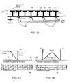
- the operations that can be performeddepend on the surface impedance, and thus the reflection phase, as a function of position. If the reflection phase assumes a linear slope 44 , the surface can be used to steer an RF beam 32 , as illustrated in FIG. 12 .
- FIG. 12demonstrates how incident beam 32 can be steered to produce a reflected beam 34 by impressing a linear reflection phase function 44 on the tunable impedance surface 30 .
- phase discontinuities of 2 ⁇can be included, so the surface acts like a diffraction grating.
- a parabolic function 46can be used to focus a reflected beam 36 , as shown in FIG. 13 .
- FIG. 13demonstrates how an incident RF beam 32 can be steered by impressing a parabolic reflection phase function 46 on the tunable impedance surface 30 .
- phase discontinuities of 2 ⁇are included, so the surface acts like a Fresnel or parabolic reflector to focus an incident wave 32 .
- the tunable impedance surface 30can be easily tuned by adjusting the capacitors 18 so that the impedance of the surface 30 varies as a function of location across the surface.
- changing the impedance profile on the tunable impedance surface 30has a profound effect on how an incident RF wave 32 interacts with the surface 30 .
- surface 30can be planar and yet act as if it were a prior art parabolic dish reflector or a diffraction grating. Even more remarkable is the fact that surface 30 can be effectively programmed to mimic not only parabolic reflectors of different sizes, but also flat, angled reflectors or any other shape of reflector or diffraction grating by simply changing the impedance of the surface as a function of location on the surface.
- the tunable impedance surface 30is depicted as being planar.
- the inventionis not limited to planar tunable impedance surfaces.
- those skilled in the artwill appreciate the fact that the printed circuit board technology preferably used to provide a substrate 24 for the tunable impedance surface 30 can provide a very flexible substrate 24 .
- the tunable impedance surface 30can be mounted on any convenient surface and conform to the shape of that surface. The tuning of the impedance function would then be adjusted to account for the shape of that surface.
- surface 30can be planar, non-planar, convex, concave or have any other shape and still act as if it were a prior art parabolic dish reflector or as a diffraction grating by appropriately tuning its surface impedance.
- the top plate elements 10 and the ground or back plane element 12are preferably formed from a metal such as copper or a copper alloy conveniently used in printed circuit board technologies. However, non-metallic, conductive materials may be used instead of metals for the top plate elements 10 and/or the ground or back plane element 12 , if desired.
Landscapes
- Physics & Mathematics (AREA)
- Optics & Photonics (AREA)
- Aerials With Secondary Devices (AREA)
Abstract
Description
This invention was made with government support under Contract No. N6601-99-C-8635. The government has certain rights in this invention.
This invention relates to a surface having a tunable electromagnetic impedance, and includes a conductive sheet of metal or other conductor, covered with an array of resonant elements, which determine the surface impedance as a function of resonance frequency. The surface impedance governs the reflection phase of the conductive sheet. Each resonant element is individually tunable by adjusting a variable capacitor, thereby controlling the electromagnetic impedance of the surface. By having a tunable, position-dependent impedance, this surface can be used to focus a reflected Radio Frequency (RF) beam by forming an effective Fresnel or parabolic reflector or to steer a reflected wave by forming an effective prism or grating. The tunable impedance surface can be used to steer or focus an RF beam, which is important in such fields as satellite communications, radar, and the like.
Prior art approaches for RF beam steering generally involve using phase shifters or mechanical gimbals. With the tunable surface disclosed herein, beam steering is accomplished by variable capacitors, thus eliminating expensive phase shifters and unreliable mechanical gimbals. The variable capacitors can be controlled electronically using variable dielectrics, or tuned using devices to impart relatively small mechanical motion such as microelectromechanical (MEM) switches.
Focusing an RF beam by a flat surface has been accomplished in the prior art by using an array of nearly resonant half-wave dipoles, which are designed to have a particular reflection phase. However, if such a structure is to include a ground plane, this prior art structure must be one-quarter wavelength thick. In the present invention, the thickness of the tunable surface is much less than one-quarter wavelength. The available bandwidth is partly determined by the tunability of the small resonant elements on the surface, which are tuned by variable capacitors.
The present application is related to U.S. patent application Ser. No. 09/537,921 entitled “An End-Fire Antenna or Array on Surface with Tunable Impedance” filed Mar. 29, 2000 and to U.S. patent application Ser. No. 09/537,722 entitled “An Electronically Tunable Reflector” filed Mar. 29, 2000 the disclosures of which are hereby incorporated herein by this reference.
The prior art includes U.S. Pat. No. 4,905,014 to Daniel G. Gonzalez, Gerald E. Pollen, and Joel F. Walker, “Microwave phasing structure for electromagnetically emulating reflective surfaces and focusing elements of selected geometry.” This patent describes placing antenna elements above a planar metallic reflector for phasing a reflected wave into a desired beam shape and location. It is a flat array that emulates differently shaped reflective surfaces (such as a dish antenna).
The prior art includes U.S. Pat. No. 5,541,614 to Juan F. Lam, Gregory L. Tangonan, and Richard L. Abrams, “Smart antenna system using microelectromechanically tunable dipole antennas and photonic bandgap materials”. This patent shows how to use RF MEMS switches and photonic bandgap surfaces for reconfigurable dipoles.
The prior art includes RF MEMS tunable dipoles ¼ wavelength above a metallic ground plane, but this approach results in limited bandwidth and limited tunability. We improve on this approach by replacing the reconfigurable dipole array with a tunable impedance surface, resulting in a thinner structure, with broader bandwidth.
The prior art further includes a pending applications of D. Sievenpiper, E. Yablonovitch, “Circuit and Method for Eliminating Surface Currents on Metals”, U.S. provisional patent application, Ser. No. 60/079,953, filed on Mar. 30, 1998.
A conventional high-impedance surface, shown in FIG. 1, consists of an array of metal top plates orelements 10 on aflat metal sheet 12. It can be fabricated using printed circuit board technology with the metal plates orelements 10 formed on a top or first surface of a printed circuit board and a solid conducting ground orback plane 12 formed on a bottom or second surface of the printed circuit board. Vertical connections are formed as metal platedvias 14 in the printed circuit board, which connect theelements 10 with theunderlying ground plane 12. The metal members, comprising thetop plates 10 and thevias 14, are arranged in a two-dimensional lattice of cells, and can be visualized as mushroom-shaped or thumbtack-shaped members protruding from theflat metal surface 12. The thickness of the structure, which is controlled by the thickness of the printed circuit board, is much less than one wavelength for the frequencies of interest. The sizes of theelements 10 are also kept less than one wavelength for the frequencies of interest. The printed circuit board is not shown for ease of illustration.
Turning to FIG. 2, the properties of this surface can be explained using an effective circuit model or cell which is assigned a surface impedance equal to that of a parallel resonant LC circuit. The use of lumped cells to describe electromagnetic structures is valid when the wavelength is much longer than the size of the individual features, as is the case here. When an electromagnetic wave interacts with the surface of FIG. 1, it causes charges to build up on the ends of thetop metal plates 10. This process can be described as governed by an effective capacitance C. As the charges slosh back and forth, in response to a radio-frequency field, they flow around a long path P through thevias 14 and thebottom metal surface 12. Associated with these currents is a magnetic field, and thus an inductance L. The capacitance C is controlled by the proximity of theadjacent metal plates 10 while the inductance L is controlled by the thickness of the structure.
The structure is inductive below the resonance and capacitive above resonance. Near the resonance frequency,

the structure exhibits high electromagnetic surface impedance.
The tangential electric field at the surface is finite, while the tangential magnetic field is zero. Thus, electromagnetic waves are reflected without the phase reversal that occurs on a flat metal sheet. In general, the reflection phase can be 0, π, or anything in between, depending on the relationship between the test frequency and the resonance frequency of the structure. The reflection phase as a function of frequency, calculated using the effective medium model, is shown in FIG.3. Far below resonance, it behaves like an ordinary metal surface, and reflects with a π phase shift. Near resonance, where the surface impedance is high, the reflection phase crosses through zero. At higher frequencies, the phase approaches −π. The calculated model of FIG. 3 is supported by the measured reflection phase, shown for an example structure in FIG.4.
A large number of structures of the type shown in FIG. 1 have been fabricated with a wide range of resonance frequencies, including various geometries and substrate materials. Some of the structure were designed with overlapping capacitor plates, to increase the capacitance and lower the frequency. The measured and calculated resonance frequencies for twenty three structures with various capacitance values are compared in FIG.5. Clearly, the resonance frequency is a predictable function of the capacitance. The dotted line in FIG. 5 has a slope of unity, and indicates perfect agreement. The bars indicate the instantaneous bandwidth of the surface, defined by the frequencies where the phase is between π/2 and −π/2.
Features of the present invention include:
1. A device with tunable surface impedance;
2. A method for focusing an electromagnetic wave using the tunable surface; and
3. A method for steering an electromagnetic wave using the tunable surface.
This invention provides a reconfigurable electromagnetic surface which is capable of performing a variety of functions, such as focusing or steering a beam. It improves upon the high-impedance surface, which is the subject of U.S. Provisional Patent Ser. No. 60/079,953, to include the important aspect of tunability, as well as several applications. The tunable structure can have any desired impedance, and thus any desired reflection phase. Therefore, by programming the surface impedance as a function of position, it can mimic such devices as a Fresnel reflector or a grating, and these properties can be reprogrammed electronically.
The present invention provides, in one aspect, a tuneable impedance surface for steering and/or focusing a radio frequency beam, the tunable surface comprising: a ground plane; a plurality of top plates disposed a distance from the ground plane, the distance being less than a wavelength of the radio frequency beam; and a capacitor arrangement for controllably varying the capacitance of adjacent top plates.
FIG. 1 depicts a conventional high-impedance surface fabricated using printed circuit board technology of the type disclosed in U.S. Provisional Patent Ser. No. 60/079,953 and having metal plates on the top side connect through metal plated vias to a solid metal ground plan on the bottom side;
FIG. 2 is a circuit equivalent of a pair of adjacent metal top plates and associated vias;
FIG. 3 depicts the calculated reflection phase of the high-impedance surface, obtained from the effective medium model and shows that the phase crosses through zero at the resonance frequency of the structure;
FIG. 4 shows that the measured reflection phase agrees well with the calculated reflection phase;
FIG. 5 depicts the measured resonance frequency compared to the calculated resonance frequency, using the effective circuit model of FIG. 2, for twenty three examples of the surface shown in FIG. 1;
FIG. 6 depicts a high impedance surface with an array of variable capacitors placed between neighboring top plates;
FIG. 7 depicts a circuit equivalent of the surface shown by FIG. 6, modified so that the addressing of each variable capacitor occurs by applying a voltage through an associated conducting via;
FIG. 8 depicts a top view of one embodiment of the present invention
FIG. 9 depicts a top view of another embodiment of the present invention;
FIG. 9adepicts a top view of one embodiment of the present invention similar to that of FIG. 9, but with all elements being controllable;
FIG. 10 depicts a top view of yet another embodiment of the present invention;
FIG. 10adepicts a top view of one embodiment of the present invention similar to that of FIG. 10, but with all elements being controllable;
FIG. 11 depicts another technique for tuning the capacitance by using heaters arranged below the surface, which heaters causing bimetallic strips on the top surface to bend;
FIG. 12 demonstrates how beam can be steered by impressing a linear reflection phase function on the tunable impedance surface—phase discontinuities of 2π are used to steer to large angles, making the surface resemble a grating; and
FIG. 13 demonstrates how a parabolic reflection phase function can be used to focus a beam.
In accordance with the present invention, a high-impedance surface is modified by addingvariable capacitors 18 as illustrated in FIG.6. Thesevariable capacitors 18 can take a variety of forms, including microelectromechanical capacitors, plunger-type actuators, thermally activated bimetallic plates, or any other device for effectively varying the capacitance between a pair ofcapacitor plates 10. Thevariable capacitors 18 can alternatively be solid state devices, in which a ferroelectric or semiconductor material provides a variable capacitance controlled by an externally applied voltage. An example is shown in FIG. 6, where individualvariable capacitors 18 are disposed between each neighboring pair of hexagonal metallictop plate elements 10. By changing the capacitance, the curves in FIGS. 3 and 4 are shifted according to the resonance frequency given by the relation:

as verified by the data depicted in FIG.5. This has the effect of changing the impedance at a single frequency. By varying the capacitance as a function of distance along (or location on) the surface, a position-dependent or location-dependent impedance can be generated on the surface30 (FIGS.6 and7), and thus a position-dependent or location-dependent reflection phase occurs. A tunable high-impedance surface 30 is thus provided.
Thevariable capacitors 18 can be provided by microelectromechanical capacitors, thermally activated bimetallic strips, plungers, or any other device for moving a capacitor plate. Alternatively,elements 18 could be semiconductor or ferroelectric variacs.
The capacitance C of a cell of the high impedance surface can be less than 1 pF. As such the amount of capacitance to be added to each cell to change the impedance can also be quite small and therefor the physical size ofelements 18 can likewise be small. Indeed,elements 18 adding capacitance in the range of 0.1 to 1.0 pF per cell will often be quite suitable.
The tunable surface of FIG. 6 is preferably built or disposed on a substrate24 (FIG. 7) such as a printed circuit board. The thickness of the printed circuit board is kept preferably much less than the wavelength associated with the frequency or frequency band of interest. For high frequency applications, that means than the printed circuit board is rather thin. Thin printed circuit boards having a thickness of only 0.1 mm are readily available For example, polyimide printed circuit boards are commercially available as thin as 1 mil (0.025 mm) and therefore the disclosed structure with printed circuit board technology can be used in very high frequency applications, if desired. Theelements 10 are electrically conductive and typically made of a metal conveniently used in printed circuit board fabrication processes and are disposed on one surface of thesubstrate 24. Theback plane 12 is disposed on the opposite surface ofsubstrate 24. Vias are typically provided and plated to formconductors 14.Conductors 14 are connected to theelements 10 at one end thereof and are coupled, either capacitively or directly, as will be discussed later, at or near another end thereof to theback plane 12.
Ifelements 18 are provided by microelectromechanical capacitors, or by solid state variacs, the capacitance can be changed by changing an applied voltage, which can be routed through theconductive vias 14. This can be accomplished by dividing the array ofelements 10 into two subsets:10aand10b.Onesubset 10ais electrically grounded, while thesecond subset 10bwould have an applied control voltage that may be different for each element insubset 10b.The control voltage is applied through a via14b,which in this case would not be connected to theground plane 12, but instead to anexternal data bus 20. This embodiment is illustrated by FIG.7. The data lines20 are fed to an external control unit (not shown) for generating the desired control voltages for various beam steering or focusing operations. In this embodiment, the data lines20 each preferably include an RF choke (not shown) wired in series to prevent radiation to the back side.
Additionally, thevias 14bare capacitively coupled to theground plane 12 so that they appear to be connected to theground plane 12 at the RF frequencies of interest, but not at the much lower frequencies of the control voltages (which would typically be considered to be comparatively slowly changing DC voltages). Since thevias 14bconveniently pass through theground plane 12, they are conveniently capacitively coupled to theground plane 12 where they penetrate theground plane 12 and that capacitance at thatpoint 14ccan be conveniently controlled using techniques well known in the art. Preferably, the capacitance at thepenetration point 14cis much larger than the capacitance ofelements 18.
FIG. 8 shows one embodiment of an hexagonal array ofelements elements 10aare directly connected to the ground plane whileelements 10bare connected to control voltages (but are capacitively or effectively coupled to the ground plane for the frequencies of the impinging RF waves of interest). The capacitances added byelements 18 are controlled by the control voltages onbus 20. Considering someparticular elements 10 identified by the letters A, B, and C in FIG. 8, it will be noted that element A is directly coupled to ground since it is a member ofsubset 10a,while elements B and C have control voltages applied thereto as they both belong tosubset 10b.Theelement 18 between elements A and B is controlled by the control voltage applied to element B through its associated via14b.The capacitance between elements A and B is controlled by (i) their physical relationship and (ii) the capacitance contributed by theaforementioned element 18. Likewise, theelement 18 between elements A and C is controlled by the control voltage applied to element C through its associated via14b.However, the capacitance between elements B and C is fixed in this embodiment by their physical relationship. Of course, anelement 18 could be provided between elements B and C in which case the capacitance contributed by that addedelement 18 would be based on the difference of the control voltages applied to elements B and C. Those skilled in the art will appreciate that such control based on voltage differences adds additional complication, since the added capacitances provided by at least some of theelements 18 are then a function of the differences in the control voltages. But if that added complication is warranted in order to provide greater control of the impedance of the surface, then even more (or perhaps all) of theelements 10 could be controlled by control voltages (in which case less or none of the elements would be directly grounded as in the case ofsubset 10a). As can be seen, the ratio of controlled (subset 10b) to uncontrolled (subset 10a)elements 10 can vary greatly.
Alternatively, all of theelements 10 can be directly connected toground plane 12 and the control voltages frombus 20 can be connected directly to the variousvariable capacitors 18 through other vias (not shown), in which case noelement 10 would be a controlled element ofsubset 10b.
FIG. 9 shows one embodiment of a rectangular arrangement of theelements subset 10b) to uncontrolled (subset 10a) elements in this figure is shown as being 1:1 and anelement 18 is disposed between eachelement 10. However, if all of theelements 18 are controlled and therefore all belong tosubset 10b(no10aelements), then the embodiment shown in FIG. 9ais arrived at. Again, the ratio of controlled (subset 10b) to uncontrolled (subset 10a)elements 10 can vary greatly.
FIG. 10 shows one embodiment of a triangular arrangement of theelements subset 10b) to uncontrolled (subset 10a) elements in this figure is shown as being 1:1 and anelement 18 is disposed by between eachelement 10. However, if all of theelements 18 were controlled by making themsubset 10belements (in whichcase subset 10ais of a zero size), then the embodiment shown in FIG. 10ais arrived at. As previously mentioned, the ratio of controlled (subset 10b) to uncontrolled (subset 10a)elements 10 can vary greatly.
The ratio of controlled (subset 10b) to uncontrolled (subset 10a)elements 10 can be less than 1:1, if desired, which will also have the effect of reducing the number ofcapacitor elements 18 utilized, but, of course, with less control of the impedance of the surface. However, that could be quite suitable in certain embodiments.
As an alternative method of tuning the capacitance, heaters26 (FIG. 11) can be arranged below the surface, which would actuate an array ofbimetallic strips 18, which would bend according to the local temperature. This embodiment is shown by FIG. 11 whereheaters 26 are provided to control the position of the adjacentbimetallic strips 18. As themetallic strips 18 move to a close position, the capacitance increases. Another method of tuning the capacitance involves mechanical plungers, which could be moved by hydraulic pressure or by a series of magnetic coils. The examples given here are not meant to limit how additional capacitance can be added. Any available technique for tuning the capacitance may be utilized.
The operations that can be performed depend on the surface impedance, and thus the reflection phase, as a function of position. If the reflection phase assumes alinear slope 44, the surface can be used to steer anRF beam 32, as illustrated in FIG.12. FIG. 12 demonstrates howincident beam 32 can be steered to produce a reflectedbeam 34 by impressing a linearreflection phase function 44 on thetunable impedance surface 30. To steer to large angles, phase discontinuities of 2π can be included, so the surface acts like a diffraction grating.
Alternatively, aparabolic function 46 can be used to focus a reflectedbeam 36, as shown in FIG.13. FIG. 13 demonstrates how anincident RF beam 32 can be steered by impressing a parabolicreflection phase function 46 on thetunable impedance surface 30. To steer to large angles, phase discontinuities of 2π are included, so the surface acts like a Fresnel or parabolic reflector to focus anincident wave 32.
Of course, thetunable impedance surface 30 can be easily tuned by adjusting thecapacitors 18 so that the impedance of thesurface 30 varies as a function of location across the surface. As can be seen by reference to FIGS. 12 and 13, changing the impedance profile on thetunable impedance surface 30 has a profound effect on how anincident RF wave 32 interacts with thesurface 30.
Indeed,surface 30 can be planar and yet act as if it were a prior art parabolic dish reflector or a diffraction grating. Even more remarkable is the fact thatsurface 30 can be effectively programmed to mimic not only parabolic reflectors of different sizes, but also flat, angled reflectors or any other shape of reflector or diffraction grating by simply changing the impedance of the surface as a function of location on the surface.
In the embodiments shown by the drawings thetunable impedance surface 30 is depicted as being planar. However, the invention is not limited to planar tunable impedance surfaces. Indeed, those skilled in the art will appreciate the fact that the printed circuit board technology preferably used to provide asubstrate 24 for thetunable impedance surface 30 can provide a veryflexible substrate 24. Thus thetunable impedance surface 30 can be mounted on any convenient surface and conform to the shape of that surface. The tuning of the impedance function would then be adjusted to account for the shape of that surface. Thus,surface 30 can be planar, non-planar, convex, concave or have any other shape and still act as if it were a prior art parabolic dish reflector or as a diffraction grating by appropriately tuning its surface impedance.
Thetop plate elements 10 and the ground orback plane element 12 are preferably formed from a metal such as copper or a copper alloy conveniently used in printed circuit board technologies. However, non-metallic, conductive materials may be used instead of metals for thetop plate elements 10 and/or the ground orback plane element 12, if desired.
Having described the invention in connection with certain embodiments thereof, modification will now certainly suggest itself to those skilled in the art. As such, the invention is not to be limited to the disclosed embodiments except as required by the appended claims.
Claims (34)
1. A tuneable impedance surface for reflecting a radio frequency beam, the tunable surface comprising:
(a) a ground plane;
(b) a plurality of elements disposed in an array a distance from the ground plane, the distance being less than a wavelength of the radio frequency beam; and
(b) a capacitor arrangement for controllably varying capacitance between at least selected ones of adjacent elements in said array.
2. The tuneable impedance surface ofclaim 1 further including a substrate having first and second major surfaces, said substrate supporting said ground plane on the first major surface thereof and supporting said plurality of elements on the second major surface thereof.
3. The tuneable impedance surface ofclaim 2 wherein said capacitor arrangement is adjustable to spatially tune the impedances of said plurality of elements.
4. The tuneable impedance surface ofclaim 3 wherein the plurality of elements each have an outside diameter which is less than the wavelength of the radio frequency beam.
5. The tuneable impedance surface ofclaim 1 wherein approximately one-half of the elements are directly or ohmically coupled to the ground plane by vias in a substrate supporting said ground plane, said plurality of elements and said capacitor arrangement.
6. The tuneable impedance surface ofclaim 5 wherein the elements which are not directly or ohmically coupled to the ground plane are coupled to a data bus for applying control voltages thereto.
7. The tuneable impedance surface ofclaim 6 wherein the elements, which are coupled to the data bus, are also capacitively coupled to the ground plane so as to appear to effectively shorted thereto for a frequency or frequencies of said radio frequency beam.
8. The tuneable impedance surface ofclaim 1 wherein less than one-half of the elements are directly or ohmically coupled to the ground plane.
9. The tuneable impedance surface ofclaim 8 wherein more than one-half of the elements are coupled to a data bus for applying control voltages thereto.
10. The tuneable impedance surface ofclaim 6 wherein the elements which are coupled to the data bus are capacitively coupled to the ground plane so as to appear to effectively shorted thereto for a frequency or frequencies of said radio frequency beam.
11. The tuneable impedance surface ofclaim 1 wherein all of the elements are coupled to a data bus for applying control voltages thereto.
12. The tuneable impedance surface ofclaim 11 wherein the elements are capacitively coupled to the ground plane so as to appear to effectively shorted thereto for a frequency or frequencies of said radio frequency beam.
13. The tuneable impedance surface ofclaim 1 wherein the capacitor arrangement includes a plurality of microelectromechanical capacitors connected between adjacent elements.
14. The tuneable impedance surface ofclaim 1 wherein the capacitor arrangement includes a plurality of variacs connected between adjacent elements.
15. The tuneable impedance surface ofclaim 1 wherein the plurality of elements are arranged in a planar array.
16. The tuneable impedance surface ofclaim 1 wherein the capacitor arrangement controllably varies the capacitance between all adjacent elements.
17. A method of tuning a high impedance surface for reflecting a radio frequency signal comprising:
arranging a plurality of generally spaced-apart conductive surfaces in an array disposed essentially parallel to and spaced from a conductive back plane, and
varying the capacitance between at least selected ones of adjacent conductive surfaces in to thereby tune the impedance of said high impedance surface.
18. The method ofclaim 17 wherein said plurality of generally spaced-apart conductive surfaces are arranged on a printed circuit board.
19. The method ofclaim 17 wherein the step varying the capacitance between adjacent conductive surfaces in said array includes connecting microelectromechanical capacitors between said at least selected ones of adjacent conductive surfaces.
20. The method ofclaim 17 wherein the capacitance is varied between all adjacent elements.
21. The method ofclaim 17 wherein the step of varying the capacitance between at least selected ones of adjacent conductive surfaces includes applied control voltages to at least selected ones of said conductive surfaces.
22. The method ofclaim 17 wherein the size of each conductive surface along a major axis thereof plane is less than a wavelength of the radio frequency signal, and preferably less than one tenth of a wavelength of the radio frequency signal, and the spacing of each conductive surface from the back plane being less than a wavelength of the radio frequency signal.
23. The method ofclaim 17 wherein the high impedance surface is tuned so that a parabolic reflection phase function is impressed on the high impedance surface.
24. The method ofclaim 23 wherein the parabolic phase function has discontinuities of 2π therein.
25. The method ofclaim 17 wherein the high impedance surface is tuned so that a linear reflection phase function is impressed on the high impedance surface.
26. The method ofclaim 25 wherein the linear phase function has discontinuities of 2π therein.
27. The method ofclaim 17 wherein the conductive surfaces are generally planar and wherein the array is generally planar.
28. The method ofclaim 17 wherein the conductive surfaces are metallic and wherein the conductive back plane is metallic.
29. A tuneable impedance surface for reflecting a radio frequency beam, the tunable surface comprising:
(a) a ground plane;
(b) a plurality of elements disposed in an array a distance from the ground plane, the distance being less than a wavelength of the radio frequency beam; and
(b) a capacitor arrangement for controllably varying the impedance along said array.
30. The method ofclaim 17 wherein the size of each conductive surface along a major axis thereof plane is than one tenth of a wavelength of the radio frequency signal and the spacing of each conductive surface from the back plane being less than a wavelength of the radio frequency signal.
31. A tunable impedance surface for reflecting a radio frequency beam impinging the surface, said tunable impedance surface comprising:
(a) a ground plane;
(b) a plurality of discreet elements disposed in a two-dimensional array a distance from the ground plane, the distance being less than a wave length of the radio frequency beam; and
(c) a plurality of capacitors coupling neighboring ones of said elements in said two dimensional array for controllably varying capacitative coupling between said neighboring ones of said elements in said two-dimensional array.
32. The reflecting surface ofclaim 31 , wherein the plurality of capacitors is provided by a plurality of microelectromechanical capacitors coupled to said neighboring ones of said elements in said two-dimensional array.
33. The surface ofclaim 31 , wherein said plurality of elements is disposed in a two-dimensional planar array and wherein said plurality of capacitors are spatially tuned whereby the tunable surface mimics a parabolic reflector to steer a reflected wave front towards a focal point.
34. The surface ofclaim 31 , further including a plurality of data lines penetrating said ground plane and coupled to selective ones of said elements in said two-dimensional array, other selected ones of said elements in said two-dimensional array being coupled to said ground plane, said plurality of data line adjustably controlling the capacitance of said plurality of capacitors in said two-dimensional array according to data on said data lines.
Priority Applications (6)
| Application Number | Priority Date | Filing Date | Title |
|---|---|---|---|
| US09/537,923US6538621B1 (en) | 2000-03-29 | 2000-03-29 | Tunable impedance surface |
| US09/589,859US6483480B1 (en) | 2000-03-29 | 2000-06-08 | Tunable impedance surface |
| AU2001253002AAU2001253002A1 (en) | 2000-03-29 | 2001-03-28 | A tunable impedance surface |
| EP01926468AEP1287589A1 (en) | 2000-03-29 | 2001-03-28 | A tunable impedance surface |
| PCT/US2001/009973WO2001073893A1 (en) | 2000-03-29 | 2001-03-28 | A tunable impedance surface |
| JP2001571509AJP2003529261A (en) | 2000-03-29 | 2001-03-28 | Tunable impedance surface |
Applications Claiming Priority (1)
| Application Number | Priority Date | Filing Date | Title |
|---|---|---|---|
| US09/537,923US6538621B1 (en) | 2000-03-29 | 2000-03-29 | Tunable impedance surface |
Related Parent Applications (1)
| Application Number | Title | Priority Date | Filing Date |
|---|---|---|---|
| US09/537,922Continuation-In-PartUS6552696B1 (en) | 2000-03-29 | 2000-03-29 | Electronically tunable reflector |
Related Child Applications (1)
| Application Number | Title | Priority Date | Filing Date |
|---|---|---|---|
| US09/589,859Continuation-In-PartUS6483480B1 (en) | 2000-03-29 | 2000-06-08 | Tunable impedance surface |
Publications (1)
| Publication Number | Publication Date |
|---|---|
| US6538621B1true US6538621B1 (en) | 2003-03-25 |
Family
ID=24144680
Family Applications (1)
| Application Number | Title | Priority Date | Filing Date |
|---|---|---|---|
| US09/537,923Expired - LifetimeUS6538621B1 (en) | 2000-03-29 | 2000-03-29 | Tunable impedance surface |
Country Status (1)
| Country | Link |
|---|---|
| US (1) | US6538621B1 (en) |
Cited By (84)
| Publication number | Priority date | Publication date | Assignee | Title |
|---|---|---|---|---|
| US20020167457A1 (en)* | 2001-04-30 | 2002-11-14 | Mckinzie William E. | Reconfigurable artificial magnetic conductor |
| US20020190655A1 (en)* | 2001-03-23 | 2002-12-19 | Chiping Chen | Vacuum electron device with a photonic bandgap structure and method of use thereof |
| US20030023417A1 (en)* | 2001-06-15 | 2003-01-30 | Chiping Chen | Photonic band gap structure simulator |
| US20030112186A1 (en)* | 2001-09-19 | 2003-06-19 | Sanchez Victor C. | Broadband antennas over electronically reconfigurable artificial magnetic conductor surfaces |
| US20030197658A1 (en)* | 2001-12-05 | 2003-10-23 | Lilly James D. | Capacitively-loaded bent-wire monopole on an artificial magnetic conductor |
| WO2003092118A1 (en)* | 2002-04-25 | 2003-11-06 | Ethertronics, Inc. | Low-profile, multi-frequency, multi-band, capacitively loaded magnetic dipole antenna |
| US20040135649A1 (en)* | 2002-05-15 | 2004-07-15 | Sievenpiper Daniel F | Single-pole multi-throw switch having low parasitic reactance, and an antenna incorporating the same |
| US20040227668A1 (en)* | 2003-05-12 | 2004-11-18 | Hrl Laboratories, Llc | Steerable leaky wave antenna capable of both forward and backward radiation |
| US20040227583A1 (en)* | 2003-05-12 | 2004-11-18 | Hrl Laboratories, Llc | RF MEMS switch with integrated impedance matching structure |
| US20040227667A1 (en)* | 2003-05-12 | 2004-11-18 | Hrl Laboratories, Llc | Meta-element antenna and array |
| US20040227678A1 (en)* | 2003-05-12 | 2004-11-18 | Hrl Laboratories, Llc | Compact tunable antenna |
| US20040263408A1 (en)* | 2003-05-12 | 2004-12-30 | Hrl Laboratories, Llc | Adaptive beam forming antenna system using a tunable impedance surface |
| US20050040918A1 (en)* | 2001-11-12 | 2005-02-24 | Per-Simon Kildal | Strip-loaded dielectric substrates for improvements of antennas and microwave devices |
| US6865402B1 (en)* | 2000-05-02 | 2005-03-08 | Bae Systems Information And Electronic Systems Integration Inc | Method and apparatus for using RF-activated MEMS switching element |
| US20050107125A1 (en)* | 2000-05-02 | 2005-05-19 | Bae Systems Information And Electronic Systems Integration Inc. | RF-actuated MEMS switching element |
| US6943730B2 (en)* | 2002-04-25 | 2005-09-13 | Ethertronics Inc. | Low-profile, multi-frequency, multi-band, capacitively loaded magnetic dipole antenna |
| US20060017651A1 (en)* | 2003-08-01 | 2006-01-26 | The Penn State Research Foundation | High-selectivity electromagnetic bandgap device and antenna system |
| US20060050010A1 (en)* | 2004-09-08 | 2006-03-09 | Jinwoo Choi | Electromagnetic bandgap structure for isolation in mixed-signal systems |
| US20060092093A1 (en)* | 2004-09-08 | 2006-05-04 | Georgia Tech Research Corporation | Mixed-signal systems with alternating impedance electromagnetic bandgap (AI-EBG) structures for noise suppression/isolation |
| US20060114170A1 (en)* | 2004-07-30 | 2006-06-01 | Hrl Laboratories, Llc | Tunable frequency selective surface |
| US20060152430A1 (en)* | 2002-09-14 | 2006-07-13 | Nigel Seddon | Periodic electromagnetic structure |
| US20060182403A1 (en)* | 2002-02-19 | 2006-08-17 | Michael Goldstein | High reflector tunable stress coating, such as for a MEMS mirror |
| US7154451B1 (en) | 2004-09-17 | 2006-12-26 | Hrl Laboratories, Llc | Large aperture rectenna based on planar lens structures |
| US20070159401A1 (en)* | 2004-02-26 | 2007-07-12 | Baliarda Carles P | Handset with electromagnetic bra |
| US20070182639A1 (en)* | 2006-02-09 | 2007-08-09 | Raytheon Company | Tunable impedance surface and method for fabricating a tunable impedance surface |
| US7298228B2 (en) | 2002-05-15 | 2007-11-20 | Hrl Laboratories, Llc | Single-pole multi-throw switch having low parasitic reactance, and an antenna incorporating the same |
| US7307589B1 (en) | 2005-12-29 | 2007-12-11 | Hrl Laboratories, Llc | Large-scale adaptive surface sensor arrays |
| US20080150657A1 (en)* | 2006-12-26 | 2008-06-26 | Motorola, Inc. | Tunable high impedance surface device |
| US20080160851A1 (en)* | 2006-12-27 | 2008-07-03 | Motorola, Inc. | Textiles Having a High Impedance Surface |
| US20080204347A1 (en)* | 2007-02-26 | 2008-08-28 | Alvey Graham R | Increasing isolation between multiple antennas with a grounded meander line structure |
| US7423608B2 (en) | 2005-12-20 | 2008-09-09 | Motorola, Inc. | High impedance electromagnetic surface and method |
| US20080238810A1 (en)* | 2007-03-30 | 2008-10-02 | Robert Scott Winsor | Radio Frequency Lens and Method of Suppressing Side-Lobes |
| US20080284674A1 (en)* | 2007-05-15 | 2008-11-20 | Hrl Laboratories, Llc | Digital control architecture for a tunable impedance surface |
| US7456803B1 (en) | 2003-05-12 | 2008-11-25 | Hrl Laboratories, Llc | Large aperture rectenna based on planar lens structures |
| US20080291101A1 (en)* | 2007-03-30 | 2008-11-27 | Itt Manufacturing Enterprises, Inc | Method and apparatus for steering and stabilizing radio frequency beams utilizing photonic crystal structures |
| US20090021444A1 (en)* | 2007-07-19 | 2009-01-22 | Kabushiki Kaisha Toshiba | High-impedance substrate |
| US20090027267A1 (en)* | 2006-02-24 | 2009-01-29 | Mbda Uk Limited | Scanned antenna system |
| US20090079824A1 (en)* | 2007-09-24 | 2009-03-26 | Robert Scott Winsor | Security Camera System and Method of Steering Beams to Alter a Field of View |
| US20090109121A1 (en)* | 2007-10-31 | 2009-04-30 | Herz Paul R | Electronically tunable microwave reflector |
| US20100053013A1 (en)* | 2006-11-22 | 2010-03-04 | Takayoshi Konishi | Ebg structure, antenna device, rfid tag, noise filter, noise absorptive sheet and wiring board with noise absorption function |
| US20100060534A1 (en)* | 2008-09-09 | 2010-03-11 | Kabushiki Kaisha Toshiba | Antenna device |
| US20100085272A1 (en)* | 2008-10-07 | 2010-04-08 | Thales | Reflector Array and Antenna Comprising Such a Reflector Array |
| US20100155127A1 (en)* | 2008-12-22 | 2010-06-24 | Fuji Xerox Co., Ltd. | Printed wiring board |
| US20100171674A1 (en)* | 2009-01-08 | 2010-07-08 | Thinkom Solutions, Inc. | Low cost electronically scanned array antenna |
| US20100171673A1 (en)* | 2007-08-22 | 2010-07-08 | Bae Systems Plc | Deployable lens antenna |
| US20100252319A1 (en)* | 2009-04-07 | 2010-10-07 | Won Woo Cho | Electromagnetic bandgap structure and printed circuit board having the same |
| US20100264316A1 (en)* | 2009-04-21 | 2010-10-21 | The Boeing Company | Compressive Millimeter Wave Imaging |
| US7868829B1 (en) | 2008-03-21 | 2011-01-11 | Hrl Laboratories, Llc | Reflectarray |
| US7911407B1 (en) | 2008-06-12 | 2011-03-22 | Hrl Laboratories, Llc | Method for designing artificial surface impedance structures characterized by an impedance tensor with complex components |
| US8018375B1 (en)* | 2010-04-11 | 2011-09-13 | Broadcom Corporation | Radar system using a projected artificial magnetic mirror |
| US8212739B2 (en) | 2007-05-15 | 2012-07-03 | Hrl Laboratories, Llc | Multiband tunable impedance surface |
| US20120206001A1 (en)* | 2011-02-16 | 2012-08-16 | Toyota Motor Engineering & Manufacturing North America, Inc. | Magnetic field focusing for actuator applications |
| US20130038147A1 (en)* | 2011-08-10 | 2013-02-14 | Toyota Motor Engineering & Manufacturing North America, Inc. | Three Dimensional Magnetic Field Manipulation in Electromagnetic Devices |
| WO2013006740A3 (en)* | 2011-07-06 | 2013-02-28 | Hrl Laboratories, Llc | Automatic tuning circuit |
| WO2012139079A3 (en)* | 2011-04-07 | 2013-02-28 | Hrl Laboratories Llc | Tunable impedance surfaces |
| US8436785B1 (en) | 2010-11-03 | 2013-05-07 | Hrl Laboratories, Llc | Electrically tunable surface impedance structure with suppressed backward wave |
| US20130241770A1 (en)* | 2011-09-14 | 2013-09-19 | Thales | Reconfigurable Radiating Phase-Shifting Cell Based on Complementary Slot and Microstrip Resonances |
| US8957831B1 (en) | 2010-03-30 | 2015-02-17 | The Boeing Company | Artificial magnetic conductors |
| US8982011B1 (en) | 2011-09-23 | 2015-03-17 | Hrl Laboratories, Llc | Conformal antennas for mitigation of structural blockage |
| US8988173B2 (en) | 2011-04-07 | 2015-03-24 | Hrl Laboratories, Llc | Differential negative impedance converters and inverters with variable or tunable conversion ratios |
| WO2015039769A1 (en) | 2013-09-18 | 2015-03-26 | Centre National De La Recherche Scientifique - Cnrs - | A wave shaping device, an electronic device, and a system |
| US8994609B2 (en) | 2011-09-23 | 2015-03-31 | Hrl Laboratories, Llc | Conformal surface wave feed |
| CN104779440A (en)* | 2015-04-17 | 2015-07-15 | 北京航空航天大学 | Intelligent three-dimensional programmable antenna reflecting surface |
| EP2975694A1 (en)* | 2014-07-14 | 2016-01-20 | Palo Alto Research Center, Incorporated | Metamaterial-based object-detection system |
| US9407239B2 (en) | 2011-07-06 | 2016-08-02 | Hrl Laboratories, Llc | Wide bandwidth automatic tuning circuit |
| US9425769B1 (en) | 2014-07-18 | 2016-08-23 | Hrl Laboratories, Llc | Optically powered and controlled non-foster circuit |
| US9466887B2 (en) | 2010-11-03 | 2016-10-11 | Hrl Laboratories, Llc | Low cost, 2D, electronically-steerable, artificial-impedance-surface antenna |
| US9559012B1 (en) | 2013-09-30 | 2017-01-31 | Hrl Laboratories, Llc | Gallium nitride complementary transistors |
| US20170141477A1 (en)* | 2015-11-13 | 2017-05-18 | Kyungpook National University Industry-Academic Cooperation Foundation | Reflection frequency conversion device using active metamaterial surface and ecm system |
| US9705201B2 (en) | 2014-02-24 | 2017-07-11 | Hrl Laboratories, Llc | Cavity-backed artificial magnetic conductor |
| US10103445B1 (en) | 2012-06-05 | 2018-10-16 | Hrl Laboratories, Llc | Cavity-backed slot antenna with an active artificial magnetic conductor |
| WO2018215415A1 (en) | 2017-05-22 | 2018-11-29 | Greenerwave | Waveform shaping device and wave receiver |
| US10193233B1 (en) | 2014-09-17 | 2019-01-29 | Hrl Laboratories, Llc | Linearly polarized active artificial magnetic conductor |
| WO2019020894A1 (en) | 2017-07-28 | 2019-01-31 | Greenerwave | Communication network access point using a waveform shaping device, communication network and wireless communication method |
| WO2019081385A1 (en) | 2017-10-25 | 2019-05-02 | Greenerwave | Display device, television set or computer monitor using such a display device |
| US10312596B2 (en) | 2013-01-17 | 2019-06-04 | Hrl Laboratories, Llc | Dual-polarization, circularly-polarized, surface-wave-waveguide, artificial-impedance-surface antenna |
| WO2019224503A2 (en) | 2018-05-25 | 2019-11-28 | Greenerwave | Method for determining a characteristic of a receiver in a medium and system implementing this method |
| FR3093210A1 (en) | 2019-02-27 | 2020-08-28 | Greenerwave | Receiver detection system |
| US10827568B2 (en) | 2014-05-13 | 2020-11-03 | Centre National de la Recherche Scientifique—CNRS | Microwave oven |
| US10983194B1 (en) | 2014-06-12 | 2021-04-20 | Hrl Laboratories, Llc | Metasurfaces for improving co-site isolation for electronic warfare applications |
| US11024952B1 (en)* | 2019-01-25 | 2021-06-01 | Hrl Laboratories, Llc | Broadband dual polarization active artificial magnetic conductor |
| US11881635B1 (en) | 2023-05-15 | 2024-01-23 | Greenerwave | Electromagnetic adjustable element and a wave shaping device including a plurality of electromagnetic adjustable elements |
| US11894613B1 (en) | 2022-01-27 | 2024-02-06 | Notch, Inc. | Metamaterial system endowing object with adjustable radar profile |
| US12124910B2 (en) | 2020-04-24 | 2024-10-22 | Greenerwave | Method and system for detecting receivers, and adjustable receiver |
Citations (53)
| Publication number | Priority date | Publication date | Assignee | Title |
|---|---|---|---|---|
| US3267480A (en) | 1961-02-23 | 1966-08-16 | Hazeltine Research Inc | Polarization converter |
| US3810183A (en) | 1970-12-18 | 1974-05-07 | Ball Brothers Res Corp | Dual slot antenna device |
| US3961333A (en) | 1974-08-29 | 1976-06-01 | Texas Instruments Incorporated | Radome wire grid having low pass frequency characteristics |
| US4150382A (en) | 1973-09-13 | 1979-04-17 | Wisconsin Alumni Research Foundation | Non-uniform variable guided wave antennas with electronically controllable scanning |
| US4266203A (en) | 1977-02-25 | 1981-05-05 | Thomson-Csf | Microwave polarization transformer |
| US4387377A (en) | 1980-06-24 | 1983-06-07 | Siemens Aktiengesellschaft | Apparatus for converting the polarization of electromagnetic waves |
| US4594595A (en) | 1984-04-18 | 1986-06-10 | Sanders Associates, Inc. | Circular log-periodic direction-finder array |
| US4749996A (en) | 1983-08-29 | 1988-06-07 | Allied-Signal Inc. | Double tuned, coupled microstrip antenna |
| US4782346A (en) | 1986-03-11 | 1988-11-01 | General Electric Company | Finline antennas |
| US4843400A (en) | 1988-08-09 | 1989-06-27 | Ford Aerospace Corporation | Aperture coupled circular polarization antenna |
| US4843403A (en) | 1987-07-29 | 1989-06-27 | Ball Corporation | Broadband notch antenna |
| US4853704A (en) | 1988-05-23 | 1989-08-01 | Ball Corporation | Notch antenna with microstrip feed |
| US4905014A (en)* | 1988-04-05 | 1990-02-27 | Malibu Research Associates, Inc. | Microwave phasing structures for electromagnetically emulating reflective surfaces and focusing elements of selected geometry |
| US5021795A (en)* | 1989-06-23 | 1991-06-04 | Motorola, Inc. | Passive temperature compensation scheme for microstrip antennas |
| US5023623A (en) | 1989-12-21 | 1991-06-11 | Hughes Aircraft Company | Dual mode antenna apparatus having slotted waveguide and broadband arrays |
| US5081466A (en) | 1990-05-04 | 1992-01-14 | Motorola, Inc. | Tapered notch antenna |
| US5115217A (en) | 1990-12-06 | 1992-05-19 | California Institute Of Technology | RF tuning element |
| US5146235A (en) | 1989-12-18 | 1992-09-08 | Akg Akustische U. Kino-Gerate Gesellschaft M.B.H. | Helical uhf transmitting and/or receiving antenna |
| US5268701A (en) | 1992-03-23 | 1993-12-07 | Raytheon Company | Radio frequency antenna |
| US5287118A (en) | 1990-07-24 | 1994-02-15 | British Aerospace Public Limited Company | Layer frequency selective surface assembly and method of modulating the power or frequency characteristics thereof |
| US5519408A (en) | 1991-01-22 | 1996-05-21 | Us Air Force | Tapered notch antenna using coplanar waveguide |
| US5525954A (en) | 1993-08-09 | 1996-06-11 | Oki Electric Industry Co., Ltd. | Stripline resonator |
| US5531018A (en) | 1993-12-20 | 1996-07-02 | General Electric Company | Method of micromachining electromagnetically actuated current switches with polyimide reinforcement seals, and switches produced thereby |
| US5534877A (en) | 1989-12-14 | 1996-07-09 | Comsat | Orthogonally polarized dual-band printed circuit antenna employing radiating elements capacitively coupled to feedlines |
| US5541614A (en) | 1995-04-04 | 1996-07-30 | Hughes Aircraft Company | Smart antenna system using microelectromechanically tunable dipole antennas and photonic bandgap materials |
| US5557291A (en) | 1995-05-25 | 1996-09-17 | Hughes Aircraft Company | Multiband, phased-array antenna with interleaved tapered-element and waveguide radiators |
| US5589845A (en)* | 1992-12-01 | 1996-12-31 | Superconducting Core Technologies, Inc. | Tuneable electric antenna apparatus including ferroelectric material |
| US5611940A (en) | 1994-04-28 | 1997-03-18 | Siemens Aktiengesellschaft | Microsystem with integrated circuit and micromechanical component, and production process |
| DE19600609A1 (en) | 1995-09-30 | 1997-04-03 | Daimler Benz Aerospace Ag | Polarisation especially for converting linear polarised wave into circular polarised wave and vice versa |
| US5638946A (en) | 1996-01-11 | 1997-06-17 | Northeastern University | Micromechanical switch with insulated switch contact |
| US5694134A (en) | 1992-12-01 | 1997-12-02 | Superconducting Core Technologies, Inc. | Phased array antenna system including a coplanar waveguide feed arrangement |
| WO1998021734A1 (en) | 1996-11-12 | 1998-05-22 | Fraunhofer-Gesellschaft zur Förderung der angewandten Forschung e.V. | Method for manufacturing a micromechanical relay |
| US5874915A (en) | 1997-08-08 | 1999-02-23 | Raytheon Company | Wideband cylindrical UHF array |
| US5894288A (en) | 1997-08-08 | 1999-04-13 | Raytheon Company | Wideband end-fire array |
| US5923303A (en) | 1997-12-24 | 1999-07-13 | U S West, Inc. | Combined space and polarization diversity antennas |
| US5945951A (en) | 1997-09-03 | 1999-08-31 | Andrew Corporation | High isolation dual polarized antenna system with microstrip-fed aperture coupled patches |
| US5949382A (en) | 1990-09-28 | 1999-09-07 | Raytheon Company | Dielectric flare notch radiator with separate transmit and receive ports |
| WO1999050929A1 (en) | 1998-03-30 | 1999-10-07 | The Regents Of The University Of California | Circuit and method for eliminating surface currents on metals |
| US6005519A (en) | 1996-09-04 | 1999-12-21 | 3 Com Corporation | Tunable microstrip antenna and method for tuning the same |
| US6040803A (en) | 1998-02-19 | 2000-03-21 | Ericsson Inc. | Dual band diversity antenna having parasitic radiating element |
| US6054659A (en) | 1998-03-09 | 2000-04-25 | General Motors Corporation | Integrated electrostatically-actuated micromachined all-metal micro-relays |
| US6075485A (en) | 1998-11-03 | 2000-06-13 | Atlantic Aerospace Electronics Corp. | Reduced weight artificial dielectric antennas and method for providing the same |
| US6081235A (en) | 1998-04-30 | 2000-06-27 | The United States Of America As Represented By The Administrator Of The National Aeronautics And Space Administration | High resolution scanning reflectarray antenna |
| WO2000044012A1 (en) | 1999-01-25 | 2000-07-27 | GFD-Gesellschaft für Diamantprodukte mbH | Microswitching contact |
| US6097343A (en) | 1998-10-23 | 2000-08-01 | Trw Inc. | Conformal load-bearing antenna system that excites aircraft structure |
| US6097263A (en) | 1996-06-28 | 2000-08-01 | Robert M. Yandrofski | Method and apparatus for electrically tuning a resonating device |
| US6118406A (en) | 1998-12-21 | 2000-09-12 | The United States Of America As Represented By The Secretary Of The Navy | Broadband direct fed phased array antenna comprising stacked patches |
| US6127908A (en) | 1997-11-17 | 2000-10-03 | Massachusetts Institute Of Technology | Microelectro-mechanical system actuator device and reconfigurable circuits utilizing same |
| US6154176A (en) | 1998-08-07 | 2000-11-28 | Sarnoff Corporation | Antennas formed using multilayer ceramic substrates |
| US6166705A (en) | 1999-07-20 | 2000-12-26 | Harris Corporation | Multi title-configured phased array antenna architecture |
| US6175337B1 (en) | 1999-09-17 | 2001-01-16 | The United States Of America As Represented By The Secretary Of The Army | High-gain, dielectric loaded, slotted waveguide antenna |
| US6191724B1 (en) | 1999-01-28 | 2001-02-20 | Mcewan Thomas E. | Short pulse microwave transceiver |
| US6246377B1 (en) | 1998-11-02 | 2001-06-12 | Fantasma Networks, Inc. | Antenna comprising two separate wideband notch regions on one coplanar substrate |
- 2000
- 2000-03-29USUS09/537,923patent/US6538621B1/ennot_activeExpired - Lifetime
Patent Citations (54)
| Publication number | Priority date | Publication date | Assignee | Title |
|---|---|---|---|---|
| US3267480A (en) | 1961-02-23 | 1966-08-16 | Hazeltine Research Inc | Polarization converter |
| US3810183A (en) | 1970-12-18 | 1974-05-07 | Ball Brothers Res Corp | Dual slot antenna device |
| US4150382A (en) | 1973-09-13 | 1979-04-17 | Wisconsin Alumni Research Foundation | Non-uniform variable guided wave antennas with electronically controllable scanning |
| US3961333A (en) | 1974-08-29 | 1976-06-01 | Texas Instruments Incorporated | Radome wire grid having low pass frequency characteristics |
| US4266203A (en) | 1977-02-25 | 1981-05-05 | Thomson-Csf | Microwave polarization transformer |
| US4387377A (en) | 1980-06-24 | 1983-06-07 | Siemens Aktiengesellschaft | Apparatus for converting the polarization of electromagnetic waves |
| US4749996A (en) | 1983-08-29 | 1988-06-07 | Allied-Signal Inc. | Double tuned, coupled microstrip antenna |
| US4594595A (en) | 1984-04-18 | 1986-06-10 | Sanders Associates, Inc. | Circular log-periodic direction-finder array |
| US4782346A (en) | 1986-03-11 | 1988-11-01 | General Electric Company | Finline antennas |
| US4843403A (en) | 1987-07-29 | 1989-06-27 | Ball Corporation | Broadband notch antenna |
| US4905014A (en)* | 1988-04-05 | 1990-02-27 | Malibu Research Associates, Inc. | Microwave phasing structures for electromagnetically emulating reflective surfaces and focusing elements of selected geometry |
| US4853704A (en) | 1988-05-23 | 1989-08-01 | Ball Corporation | Notch antenna with microstrip feed |
| US4843400A (en) | 1988-08-09 | 1989-06-27 | Ford Aerospace Corporation | Aperture coupled circular polarization antenna |
| US5021795A (en)* | 1989-06-23 | 1991-06-04 | Motorola, Inc. | Passive temperature compensation scheme for microstrip antennas |
| US5534877A (en) | 1989-12-14 | 1996-07-09 | Comsat | Orthogonally polarized dual-band printed circuit antenna employing radiating elements capacitively coupled to feedlines |
| US5146235A (en) | 1989-12-18 | 1992-09-08 | Akg Akustische U. Kino-Gerate Gesellschaft M.B.H. | Helical uhf transmitting and/or receiving antenna |
| US5023623A (en) | 1989-12-21 | 1991-06-11 | Hughes Aircraft Company | Dual mode antenna apparatus having slotted waveguide and broadband arrays |
| US5081466A (en) | 1990-05-04 | 1992-01-14 | Motorola, Inc. | Tapered notch antenna |
| US5287118A (en) | 1990-07-24 | 1994-02-15 | British Aerospace Public Limited Company | Layer frequency selective surface assembly and method of modulating the power or frequency characteristics thereof |
| US5949382A (en) | 1990-09-28 | 1999-09-07 | Raytheon Company | Dielectric flare notch radiator with separate transmit and receive ports |
| US5115217A (en) | 1990-12-06 | 1992-05-19 | California Institute Of Technology | RF tuning element |
| US5519408A (en) | 1991-01-22 | 1996-05-21 | Us Air Force | Tapered notch antenna using coplanar waveguide |
| US5268701A (en) | 1992-03-23 | 1993-12-07 | Raytheon Company | Radio frequency antenna |
| US5721194A (en) | 1992-12-01 | 1998-02-24 | Superconducting Core Technologies, Inc. | Tuneable microwave devices including fringe effect capacitor incorporating ferroelectric films |
| US5589845A (en)* | 1992-12-01 | 1996-12-31 | Superconducting Core Technologies, Inc. | Tuneable electric antenna apparatus including ferroelectric material |
| US5694134A (en) | 1992-12-01 | 1997-12-02 | Superconducting Core Technologies, Inc. | Phased array antenna system including a coplanar waveguide feed arrangement |
| US5525954A (en) | 1993-08-09 | 1996-06-11 | Oki Electric Industry Co., Ltd. | Stripline resonator |
| US5531018A (en) | 1993-12-20 | 1996-07-02 | General Electric Company | Method of micromachining electromagnetically actuated current switches with polyimide reinforcement seals, and switches produced thereby |
| US5611940A (en) | 1994-04-28 | 1997-03-18 | Siemens Aktiengesellschaft | Microsystem with integrated circuit and micromechanical component, and production process |
| US5541614A (en) | 1995-04-04 | 1996-07-30 | Hughes Aircraft Company | Smart antenna system using microelectromechanically tunable dipole antennas and photonic bandgap materials |
| US5557291A (en) | 1995-05-25 | 1996-09-17 | Hughes Aircraft Company | Multiband, phased-array antenna with interleaved tapered-element and waveguide radiators |
| DE19600609A1 (en) | 1995-09-30 | 1997-04-03 | Daimler Benz Aerospace Ag | Polarisation especially for converting linear polarised wave into circular polarised wave and vice versa |
| US5638946A (en) | 1996-01-11 | 1997-06-17 | Northeastern University | Micromechanical switch with insulated switch contact |
| US6097263A (en) | 1996-06-28 | 2000-08-01 | Robert M. Yandrofski | Method and apparatus for electrically tuning a resonating device |
| US6005519A (en) | 1996-09-04 | 1999-12-21 | 3 Com Corporation | Tunable microstrip antenna and method for tuning the same |
| WO1998021734A1 (en) | 1996-11-12 | 1998-05-22 | Fraunhofer-Gesellschaft zur Förderung der angewandten Forschung e.V. | Method for manufacturing a micromechanical relay |
| US5874915A (en) | 1997-08-08 | 1999-02-23 | Raytheon Company | Wideband cylindrical UHF array |
| US5894288A (en) | 1997-08-08 | 1999-04-13 | Raytheon Company | Wideband end-fire array |
| US5945951A (en) | 1997-09-03 | 1999-08-31 | Andrew Corporation | High isolation dual polarized antenna system with microstrip-fed aperture coupled patches |
| US6127908A (en) | 1997-11-17 | 2000-10-03 | Massachusetts Institute Of Technology | Microelectro-mechanical system actuator device and reconfigurable circuits utilizing same |
| US5923303A (en) | 1997-12-24 | 1999-07-13 | U S West, Inc. | Combined space and polarization diversity antennas |
| US6040803A (en) | 1998-02-19 | 2000-03-21 | Ericsson Inc. | Dual band diversity antenna having parasitic radiating element |
| US6054659A (en) | 1998-03-09 | 2000-04-25 | General Motors Corporation | Integrated electrostatically-actuated micromachined all-metal micro-relays |
| WO1999050929A1 (en) | 1998-03-30 | 1999-10-07 | The Regents Of The University Of California | Circuit and method for eliminating surface currents on metals |
| US6081235A (en) | 1998-04-30 | 2000-06-27 | The United States Of America As Represented By The Administrator Of The National Aeronautics And Space Administration | High resolution scanning reflectarray antenna |
| US6154176A (en) | 1998-08-07 | 2000-11-28 | Sarnoff Corporation | Antennas formed using multilayer ceramic substrates |
| US6097343A (en) | 1998-10-23 | 2000-08-01 | Trw Inc. | Conformal load-bearing antenna system that excites aircraft structure |
| US6246377B1 (en) | 1998-11-02 | 2001-06-12 | Fantasma Networks, Inc. | Antenna comprising two separate wideband notch regions on one coplanar substrate |
| US6075485A (en) | 1998-11-03 | 2000-06-13 | Atlantic Aerospace Electronics Corp. | Reduced weight artificial dielectric antennas and method for providing the same |
| US6118406A (en) | 1998-12-21 | 2000-09-12 | The United States Of America As Represented By The Secretary Of The Navy | Broadband direct fed phased array antenna comprising stacked patches |
| WO2000044012A1 (en) | 1999-01-25 | 2000-07-27 | GFD-Gesellschaft für Diamantprodukte mbH | Microswitching contact |
| US6191724B1 (en) | 1999-01-28 | 2001-02-20 | Mcewan Thomas E. | Short pulse microwave transceiver |
| US6166705A (en) | 1999-07-20 | 2000-12-26 | Harris Corporation | Multi title-configured phased array antenna architecture |
| US6175337B1 (en) | 1999-09-17 | 2001-01-16 | The United States Of America As Represented By The Secretary Of The Army | High-gain, dielectric loaded, slotted waveguide antenna |
Non-Patent Citations (11)
| Title |
|---|
| Balanis, C., "Aperture Antennas", Antenna Theory, Analysis, and Design, 2nd Edition, (New York, John Wiley & Sons, 1997), Chap. 12, pp. 575-597. |
| Balanis, C., "Microstrip Antennas", Antenna Theory, Analysis and Design, 2nd Edition, (New York, John Wiley & Sons, 1997), Chap. 14, pp. 722-736. |
| Bradley, T.W., et al., "Development of a Voltage-Variable Dielectric (VVD), Electronic Scan Antenna," Radar 97, Publication No. 449, pp. 383-385 (Oct. 1997). |
| Cognard, J., "Alignment of Nematic Liquid Crystals and Their Mixtures" Mol. Cryst. Lig, Cryst. Suppl. 1, 1 (1982) pp. 1-74. |
| Doane, J.W., et al., "Field Controlled Light Scattering from Nematic Microdroplets", Applied Physics Letters, vol. 48 (Jan. 1986) pp. 269-271. |
| Jensen, M.A., et al., "EM Interaction of Handset Antennas and a Human in Personal Communications", Proceedings of the IEEE, vol. 83, No. 1 (Jan. 1995) pp. 7-17. |
| Jensen, M.A., et al., "Performance Analysis of Antennas for Hand-held Transceivers using FDTD", IEEE Transactions on Antennas and Propagation, vol. 42, No. 8 (Aug. 1994) pp. 1106-1113. |
| Ramo, S., et al., Fields and Waves in Communications Electronics, 3rd Edition (New York) John Wiley & Sons, 1994) Section 9.8-9.11, pp. 476-487. |
| Sievenpiper, D., "High-Impedance Electromagnetic Surfaces", Ph.D. Dissertation, Dept. of Electrical Engineering, University of California, Los Angeles, CA, 1999. |
| Sievenpiper, D., et al., "High-Impedance Electromagnetic Surfaces with a Forbidden Frequency Band", IEEE Transaction on Microwave Theory and Techniques, vol. 47, No. 11, (Nov. 1999) pp. 2059-2074. |
| Wu, S.T., et al., "High Birefringence and Wide Nematic Range Bis-tolane Liquid Crystals", Applied Physics Letters vol. 74, No. 5, (Jan. 1999) pp. 344-346. |
Cited By (149)
| Publication number | Priority date | Publication date | Assignee | Title |
|---|---|---|---|---|
| US6865402B1 (en)* | 2000-05-02 | 2005-03-08 | Bae Systems Information And Electronic Systems Integration Inc | Method and apparatus for using RF-activated MEMS switching element |
| US20050107125A1 (en)* | 2000-05-02 | 2005-05-19 | Bae Systems Information And Electronic Systems Integration Inc. | RF-actuated MEMS switching element |
| US7228156B2 (en)* | 2000-05-02 | 2007-06-05 | Bae Systems Information And Electronic Systems Integration Inc. | RF-actuated MEMS switching element |
| US6801107B2 (en)* | 2001-03-23 | 2004-10-05 | Massachusetts Institute Of Technology | Vacuum electron device with a photonic bandgap structure and method of use thereof |
| US20020190655A1 (en)* | 2001-03-23 | 2002-12-19 | Chiping Chen | Vacuum electron device with a photonic bandgap structure and method of use thereof |
| US20020167457A1 (en)* | 2001-04-30 | 2002-11-14 | Mckinzie William E. | Reconfigurable artificial magnetic conductor |
| US6897831B2 (en)* | 2001-04-30 | 2005-05-24 | Titan Aerospace Electronic Division | Reconfigurable artificial magnetic conductor |
| US7117133B2 (en) | 2001-06-15 | 2006-10-03 | Massachusetts Institute Of Technology | Photonic band gap structure simulator |
| US20030023417A1 (en)* | 2001-06-15 | 2003-01-30 | Chiping Chen | Photonic band gap structure simulator |
| US6917343B2 (en)* | 2001-09-19 | 2005-07-12 | Titan Aerospace Electronics Division | Broadband antennas over electronically reconfigurable artificial magnetic conductor surfaces |
| US20030112186A1 (en)* | 2001-09-19 | 2003-06-19 | Sanchez Victor C. | Broadband antennas over electronically reconfigurable artificial magnetic conductor surfaces |
| US20050040918A1 (en)* | 2001-11-12 | 2005-02-24 | Per-Simon Kildal | Strip-loaded dielectric substrates for improvements of antennas and microwave devices |
| US6768476B2 (en)* | 2001-12-05 | 2004-07-27 | Etenna Corporation | Capacitively-loaded bent-wire monopole on an artificial magnetic conductor |
| US20030197658A1 (en)* | 2001-12-05 | 2003-10-23 | Lilly James D. | Capacitively-loaded bent-wire monopole on an artificial magnetic conductor |
| US7355268B2 (en)* | 2002-02-19 | 2008-04-08 | Intel Corporation | High reflector tunable stress coating, such as for a MEMS mirror |
| US20060182403A1 (en)* | 2002-02-19 | 2006-08-17 | Michael Goldstein | High reflector tunable stress coating, such as for a MEMS mirror |
| WO2003092118A1 (en)* | 2002-04-25 | 2003-11-06 | Ethertronics, Inc. | Low-profile, multi-frequency, multi-band, capacitively loaded magnetic dipole antenna |
| US6943730B2 (en)* | 2002-04-25 | 2005-09-13 | Ethertronics Inc. | Low-profile, multi-frequency, multi-band, capacitively loaded magnetic dipole antenna |
| US7276990B2 (en) | 2002-05-15 | 2007-10-02 | Hrl Laboratories, Llc | Single-pole multi-throw switch having low parasitic reactance, and an antenna incorporating the same |
| US20040135649A1 (en)* | 2002-05-15 | 2004-07-15 | Sievenpiper Daniel F | Single-pole multi-throw switch having low parasitic reactance, and an antenna incorporating the same |
| US7298228B2 (en) | 2002-05-15 | 2007-11-20 | Hrl Laboratories, Llc | Single-pole multi-throw switch having low parasitic reactance, and an antenna incorporating the same |
| US20060152430A1 (en)* | 2002-09-14 | 2006-07-13 | Nigel Seddon | Periodic electromagnetic structure |
| US20040263408A1 (en)* | 2003-05-12 | 2004-12-30 | Hrl Laboratories, Llc | Adaptive beam forming antenna system using a tunable impedance surface |
| US20040227583A1 (en)* | 2003-05-12 | 2004-11-18 | Hrl Laboratories, Llc | RF MEMS switch with integrated impedance matching structure |
| US20040227668A1 (en)* | 2003-05-12 | 2004-11-18 | Hrl Laboratories, Llc | Steerable leaky wave antenna capable of both forward and backward radiation |
| US7068234B2 (en) | 2003-05-12 | 2006-06-27 | Hrl Laboratories, Llc | Meta-element antenna and array |
| US7071888B2 (en)* | 2003-05-12 | 2006-07-04 | Hrl Laboratories, Llc | Steerable leaky wave antenna capable of both forward and backward radiation |
| US7245269B2 (en) | 2003-05-12 | 2007-07-17 | Hrl Laboratories, Llc | Adaptive beam forming antenna system using a tunable impedance surface |
| US7253699B2 (en) | 2003-05-12 | 2007-08-07 | Hrl Laboratories, Llc | RF MEMS switch with integrated impedance matching structure |
| US20040227667A1 (en)* | 2003-05-12 | 2004-11-18 | Hrl Laboratories, Llc | Meta-element antenna and array |
| US7456803B1 (en) | 2003-05-12 | 2008-11-25 | Hrl Laboratories, Llc | Large aperture rectenna based on planar lens structures |
| US7164387B2 (en) | 2003-05-12 | 2007-01-16 | Hrl Laboratories, Llc | Compact tunable antenna |
| US20040227678A1 (en)* | 2003-05-12 | 2004-11-18 | Hrl Laboratories, Llc | Compact tunable antenna |
| US7042419B2 (en) | 2003-08-01 | 2006-05-09 | The Penn State Reserach Foundation | High-selectivity electromagnetic bandgap device and antenna system |
| US20060017651A1 (en)* | 2003-08-01 | 2006-01-26 | The Penn State Research Foundation | High-selectivity electromagnetic bandgap device and antenna system |
| US7456792B2 (en) | 2004-02-26 | 2008-11-25 | Fractus, S.A. | Handset with electromagnetic bra |
| US20070159401A1 (en)* | 2004-02-26 | 2007-07-12 | Baliarda Carles P | Handset with electromagnetic bra |
| US8063833B2 (en) | 2004-07-30 | 2011-11-22 | Hrl Laboratories, Llc | Method of achieving an opaque or absorption state in a tunable frequency selective surface |
| US20100073261A1 (en)* | 2004-07-30 | 2010-03-25 | Hrl Laboratories, Llc | Tunable frequency selective surface |
| US7612718B2 (en) | 2004-07-30 | 2009-11-03 | Hrl Laboratories, Llc | Tunable frequency selective surface |
| US20070085757A1 (en)* | 2004-07-30 | 2007-04-19 | Hrl Laboratories, Llc | Tunable frequency selective surface |
| US7173565B2 (en) | 2004-07-30 | 2007-02-06 | Hrl Laboratories, Llc | Tunable frequency selective surface |
| US20060114170A1 (en)* | 2004-07-30 | 2006-06-01 | Hrl Laboratories, Llc | Tunable frequency selective surface |
| US8339320B2 (en) | 2004-07-30 | 2012-12-25 | Hrl Laboratories, Llc | Tunable frequency selective surface |
| US20060050010A1 (en)* | 2004-09-08 | 2006-03-09 | Jinwoo Choi | Electromagnetic bandgap structure for isolation in mixed-signal systems |
| US7215301B2 (en)* | 2004-09-08 | 2007-05-08 | Georgia Tech Research Corporation | Electromagnetic bandgap structure for isolation in mixed-signal systems |
| US20060092093A1 (en)* | 2004-09-08 | 2006-05-04 | Georgia Tech Research Corporation | Mixed-signal systems with alternating impedance electromagnetic bandgap (AI-EBG) structures for noise suppression/isolation |
| US7253788B2 (en) | 2004-09-08 | 2007-08-07 | Georgia Tech Research Corp. | Mixed-signal systems with alternating impedance electromagnetic bandgap (AI-EBG) structures for noise suppression/isolation |
| US7154451B1 (en) | 2004-09-17 | 2006-12-26 | Hrl Laboratories, Llc | Large aperture rectenna based on planar lens structures |
| US7528788B2 (en) | 2005-12-20 | 2009-05-05 | Motorola, Inc. | High impedance electromagnetic surface and method |
| US7423608B2 (en) | 2005-12-20 | 2008-09-09 | Motorola, Inc. | High impedance electromagnetic surface and method |
| US20080272982A1 (en)* | 2005-12-20 | 2008-11-06 | Motorola, Inc. | High impedance electromagnetic surface and method |
| US7307589B1 (en) | 2005-12-29 | 2007-12-11 | Hrl Laboratories, Llc | Large-scale adaptive surface sensor arrays |
| US7683854B2 (en) | 2006-02-09 | 2010-03-23 | Raytheon Company | Tunable impedance surface and method for fabricating a tunable impedance surface |
| US20070182639A1 (en)* | 2006-02-09 | 2007-08-09 | Raytheon Company | Tunable impedance surface and method for fabricating a tunable impedance surface |
| US7808430B2 (en) | 2006-02-24 | 2010-10-05 | Mbda Uk Limited | Scanned antenna system |
| US20090027267A1 (en)* | 2006-02-24 | 2009-01-29 | Mbda Uk Limited | Scanned antenna system |
| US20100053013A1 (en)* | 2006-11-22 | 2010-03-04 | Takayoshi Konishi | Ebg structure, antenna device, rfid tag, noise filter, noise absorptive sheet and wiring board with noise absorption function |
| US8514147B2 (en) | 2006-11-22 | 2013-08-20 | Nec Tokin Corporation | EBG structure, antenna device, RFID tag, noise filter, noise absorptive sheet and wiring board with noise absorption function |
| US7518465B2 (en) | 2006-12-26 | 2009-04-14 | Motorola, Inc. | Tunable high impedance surface device |
| US20080150657A1 (en)* | 2006-12-26 | 2008-06-26 | Motorola, Inc. | Tunable high impedance surface device |
| US20080160851A1 (en)* | 2006-12-27 | 2008-07-03 | Motorola, Inc. | Textiles Having a High Impedance Surface |
| US20080204347A1 (en)* | 2007-02-26 | 2008-08-28 | Alvey Graham R | Increasing isolation between multiple antennas with a grounded meander line structure |
| US7701395B2 (en) | 2007-02-26 | 2010-04-20 | The Board Of Trustees Of The University Of Illinois | Increasing isolation between multiple antennas with a grounded meander line structure |
| US7642978B2 (en)* | 2007-03-30 | 2010-01-05 | Itt Manufacturing Enterprises, Inc. | Method and apparatus for steering and stabilizing radio frequency beams utilizing photonic crystal structures |
| US7777690B2 (en) | 2007-03-30 | 2010-08-17 | Itt Manufacturing Enterprises, Inc. | Radio frequency lens and method of suppressing side-lobes |
| US20080291101A1 (en)* | 2007-03-30 | 2008-11-27 | Itt Manufacturing Enterprises, Inc | Method and apparatus for steering and stabilizing radio frequency beams utilizing photonic crystal structures |
| US20080238810A1 (en)* | 2007-03-30 | 2008-10-02 | Robert Scott Winsor | Radio Frequency Lens and Method of Suppressing Side-Lobes |
| US8212739B2 (en) | 2007-05-15 | 2012-07-03 | Hrl Laboratories, Llc | Multiband tunable impedance surface |
| US20080284674A1 (en)* | 2007-05-15 | 2008-11-20 | Hrl Laboratories, Llc | Digital control architecture for a tunable impedance surface |
| US20090021444A1 (en)* | 2007-07-19 | 2009-01-22 | Kabushiki Kaisha Toshiba | High-impedance substrate |
| US7936310B2 (en)* | 2007-07-19 | 2011-05-03 | Kabushiki Kaisha Toshiba | High-impedance substrate |
| US20100171673A1 (en)* | 2007-08-22 | 2010-07-08 | Bae Systems Plc | Deployable lens antenna |
| US8077102B2 (en)* | 2007-08-22 | 2011-12-13 | Bae Systems Plc | Deployable lens antenna |
| US20090079824A1 (en)* | 2007-09-24 | 2009-03-26 | Robert Scott Winsor | Security Camera System and Method of Steering Beams to Alter a Field of View |
| US8614743B2 (en) | 2007-09-24 | 2013-12-24 | Exelis Inc. | Security camera system and method of steering beams to alter a field of view |
| US20090109121A1 (en)* | 2007-10-31 | 2009-04-30 | Herz Paul R | Electronically tunable microwave reflector |
| US8134521B2 (en)* | 2007-10-31 | 2012-03-13 | Raytheon Company | Electronically tunable microwave reflector |
| US7868829B1 (en) | 2008-03-21 | 2011-01-11 | Hrl Laboratories, Llc | Reflectarray |
| US7911407B1 (en) | 2008-06-12 | 2011-03-22 | Hrl Laboratories, Llc | Method for designing artificial surface impedance structures characterized by an impedance tensor with complex components |
| US20100060534A1 (en)* | 2008-09-09 | 2010-03-11 | Kabushiki Kaisha Toshiba | Antenna device |
| US20100085272A1 (en)* | 2008-10-07 | 2010-04-08 | Thales | Reflector Array and Antenna Comprising Such a Reflector Array |
| US8319698B2 (en)* | 2008-10-07 | 2012-11-27 | Thales | Reflector array and antenna comprising such a reflector array |
| US8541692B2 (en)* | 2008-12-22 | 2013-09-24 | Fuji Xerox Co., Ltd. | Printed wiring board |
| US20100155127A1 (en)* | 2008-12-22 | 2010-06-24 | Fuji Xerox Co., Ltd. | Printed wiring board |
| US20100171674A1 (en)* | 2009-01-08 | 2010-07-08 | Thinkom Solutions, Inc. | Low cost electronically scanned array antenna |
| US8362965B2 (en) | 2009-01-08 | 2013-01-29 | Thinkom Solutions, Inc. | Low cost electronically scanned array antenna |
| US20100252319A1 (en)* | 2009-04-07 | 2010-10-07 | Won Woo Cho | Electromagnetic bandgap structure and printed circuit board having the same |
| US8330048B2 (en)* | 2009-04-07 | 2012-12-11 | Samsung Electro-Mechanics Co., Ltd. | Electromagnetic bandgap structure and printed circuit board having the same |
| US8263939B2 (en) | 2009-04-21 | 2012-09-11 | The Boeing Company | Compressive millimeter wave imaging |
| US20100264316A1 (en)* | 2009-04-21 | 2010-10-21 | The Boeing Company | Compressive Millimeter Wave Imaging |
| US8957831B1 (en) | 2010-03-30 | 2015-02-17 | The Boeing Company | Artificial magnetic conductors |
| US8018375B1 (en)* | 2010-04-11 | 2011-09-13 | Broadcom Corporation | Radar system using a projected artificial magnetic mirror |
| US9466887B2 (en) | 2010-11-03 | 2016-10-11 | Hrl Laboratories, Llc | Low cost, 2D, electronically-steerable, artificial-impedance-surface antenna |
| US8436785B1 (en) | 2010-11-03 | 2013-05-07 | Hrl Laboratories, Llc | Electrically tunable surface impedance structure with suppressed backward wave |
| US20120206001A1 (en)* | 2011-02-16 | 2012-08-16 | Toyota Motor Engineering & Manufacturing North America, Inc. | Magnetic field focusing for actuator applications |
| US8736136B2 (en)* | 2011-02-16 | 2014-05-27 | Toyota Motor Engineering & Manufacturing North America, Inc. | Magnetic field manipulation in switched reluctance motors and design method |
| US8976077B2 (en) | 2011-04-07 | 2015-03-10 | Hrl Laboratories, Llc | Widebrand adaptable artificial impedance surface |
| WO2012139079A3 (en)* | 2011-04-07 | 2013-02-28 | Hrl Laboratories Llc | Tunable impedance surfaces |
| US9379448B2 (en)* | 2011-04-07 | 2016-06-28 | Hrl Laboratories, Llc | Polarization independent active artificial magnetic conductor |
| US8988173B2 (en) | 2011-04-07 | 2015-03-24 | Hrl Laboratories, Llc | Differential negative impedance converters and inverters with variable or tunable conversion ratios |
| US20150244080A1 (en)* | 2011-04-07 | 2015-08-27 | Hrl Laboratories, Llc. | Polarization independent active artificial magentic conductor |
| WO2013006740A3 (en)* | 2011-07-06 | 2013-02-28 | Hrl Laboratories, Llc | Automatic tuning circuit |
| US9407239B2 (en) | 2011-07-06 | 2016-08-02 | Hrl Laboratories, Llc | Wide bandwidth automatic tuning circuit |
| CN103797719A (en)* | 2011-07-06 | 2014-05-14 | Hrl实验室有限责任公司 | Automatic tuning circuit |
| CN103797719B (en)* | 2011-07-06 | 2016-06-01 | Hrl实验室有限责任公司 | Automatic tuning circuit and a kind of method making antenna mate with radio receiver |
| US20130038147A1 (en)* | 2011-08-10 | 2013-02-14 | Toyota Motor Engineering & Manufacturing North America, Inc. | Three Dimensional Magnetic Field Manipulation in Electromagnetic Devices |
| US8736128B2 (en)* | 2011-08-10 | 2014-05-27 | Toyota Motor Engineering & Manufacturing North America, Inc. | Three dimensional magnetic field manipulation in electromagnetic devices |
| US20130241770A1 (en)* | 2011-09-14 | 2013-09-19 | Thales | Reconfigurable Radiating Phase-Shifting Cell Based on Complementary Slot and Microstrip Resonances |
| US9647336B2 (en)* | 2011-09-14 | 2017-05-09 | Thales | Reconfigurable radiating phase-shifting cell based on complementary slot and microstrip resonances |
| US8994609B2 (en) | 2011-09-23 | 2015-03-31 | Hrl Laboratories, Llc | Conformal surface wave feed |
| US8982011B1 (en) | 2011-09-23 | 2015-03-17 | Hrl Laboratories, Llc | Conformal antennas for mitigation of structural blockage |
| US10103445B1 (en) | 2012-06-05 | 2018-10-16 | Hrl Laboratories, Llc | Cavity-backed slot antenna with an active artificial magnetic conductor |
| US10312596B2 (en) | 2013-01-17 | 2019-06-04 | Hrl Laboratories, Llc | Dual-polarization, circularly-polarized, surface-wave-waveguide, artificial-impedance-surface antenna |
| US20220131624A1 (en)* | 2013-09-18 | 2022-04-28 | Centre National De La Recherche Scientifique - Cnrs | Wave shaping device, an electronic device, and a system |
| US11251886B2 (en) | 2013-09-18 | 2022-02-15 | Centre National de la Recherche Scientifique—CNRS | Wave shaping device, an electronic device, and a system |
| US11784732B2 (en)* | 2013-09-18 | 2023-10-10 | Centre National de la Recherche Scientifique—CNRS | Wave shaping device, an electronic device, and a system |
| WO2015039769A1 (en) | 2013-09-18 | 2015-03-26 | Centre National De La Recherche Scientifique - Cnrs - | A wave shaping device, an electronic device, and a system |
| US9559012B1 (en) | 2013-09-30 | 2017-01-31 | Hrl Laboratories, Llc | Gallium nitride complementary transistors |
| US9705201B2 (en) | 2014-02-24 | 2017-07-11 | Hrl Laboratories, Llc | Cavity-backed artificial magnetic conductor |
| US10827568B2 (en) | 2014-05-13 | 2020-11-03 | Centre National de la Recherche Scientifique—CNRS | Microwave oven |
| US10983194B1 (en) | 2014-06-12 | 2021-04-20 | Hrl Laboratories, Llc | Metasurfaces for improving co-site isolation for electronic warfare applications |
| JP2016020899A (en)* | 2014-07-14 | 2016-02-04 | パロ アルト リサーチ センター インコーポレイテッド | Metamaterial-based object-detection system |
| EP2975694A1 (en)* | 2014-07-14 | 2016-01-20 | Palo Alto Research Center, Incorporated | Metamaterial-based object-detection system |
| US9425769B1 (en) | 2014-07-18 | 2016-08-23 | Hrl Laboratories, Llc | Optically powered and controlled non-foster circuit |
| US10193233B1 (en) | 2014-09-17 | 2019-01-29 | Hrl Laboratories, Llc | Linearly polarized active artificial magnetic conductor |
| CN104779440B (en)* | 2015-04-17 | 2017-09-12 | 北京航空航天大学 | A kind of intelligent three-dimensional programmable antenna reflecting surface |
| CN104779440A (en)* | 2015-04-17 | 2015-07-15 | 北京航空航天大学 | Intelligent three-dimensional programmable antenna reflecting surface |
| US20170141477A1 (en)* | 2015-11-13 | 2017-05-18 | Kyungpook National University Industry-Academic Cooperation Foundation | Reflection frequency conversion device using active metamaterial surface and ecm system |
| US10498042B2 (en)* | 2015-11-13 | 2019-12-03 | Kyungpook National University Industry-Academic Cooperation Foundation | Reflection frequency conversion device using active metamaterial surface and ECM system |
| US10805127B2 (en) | 2017-05-22 | 2020-10-13 | Greenerwave | Waveform shaping device and wave receiver |
| WO2018215415A1 (en) | 2017-05-22 | 2018-11-29 | Greenerwave | Waveform shaping device and wave receiver |
| US20220329377A1 (en)* | 2017-07-28 | 2022-10-13 | Greenerwave | Communication network access point, communication network, and method of wireless communication |
| US11290231B2 (en) | 2017-07-28 | 2022-03-29 | Greenerwave | Communication network access point, communication network, and method of wireless communication |
| KR20200088267A (en)* | 2017-07-28 | 2020-07-22 | 그리너웨이브 | Wireless network access point, communication network and wireless communication method |
| KR102515988B1 (en) | 2017-07-28 | 2023-03-31 | 그리너웨이브 | Wireless network access point, communication network and wireless communication method |
| WO2019020894A1 (en) | 2017-07-28 | 2019-01-31 | Greenerwave | Communication network access point using a waveform shaping device, communication network and wireless communication method |
| US11606530B2 (en) | 2017-10-25 | 2023-03-14 | Greenewave | Display device, television set or computer monitor using such a display device |
| WO2019081385A1 (en) | 2017-10-25 | 2019-05-02 | Greenerwave | Display device, television set or computer monitor using such a display device |
| WO2019224503A2 (en) | 2018-05-25 | 2019-11-28 | Greenerwave | Method for determining a characteristic of a receiver in a medium and system implementing this method |
| US11024952B1 (en)* | 2019-01-25 | 2021-06-01 | Hrl Laboratories, Llc | Broadband dual polarization active artificial magnetic conductor |
| US20220121829A1 (en)* | 2019-02-27 | 2022-04-21 | Greenerwave | System for detecting receivers |
| WO2020174151A1 (en) | 2019-02-27 | 2020-09-03 | Greenerwave | System for detecting receivers |
| FR3093210A1 (en) | 2019-02-27 | 2020-08-28 | Greenerwave | Receiver detection system |
| US11797786B2 (en)* | 2019-02-27 | 2023-10-24 | Greenerwave | System for detecting receivers |
| US12124910B2 (en) | 2020-04-24 | 2024-10-22 | Greenerwave | Method and system for detecting receivers, and adjustable receiver |
| US11894613B1 (en) | 2022-01-27 | 2024-02-06 | Notch, Inc. | Metamaterial system endowing object with adjustable radar profile |
| US11881635B1 (en) | 2023-05-15 | 2024-01-23 | Greenerwave | Electromagnetic adjustable element and a wave shaping device including a plurality of electromagnetic adjustable elements |
| WO2024235886A1 (en) | 2023-05-15 | 2024-11-21 | Greenerwave | An electromagnetic adjustable element and a wave shaping device including a plurality of electromagnetic adjustable elements |
Similar Documents
| Publication | Publication Date | Title |
|---|---|---|
| US6538621B1 (en) | Tunable impedance surface | |
| US6483480B1 (en) | Tunable impedance surface | |
| EP3850706B1 (en) | Electronically steerable holographic antenna with reconfigurable radiators for wideband frequency tuning | |
| US6384797B1 (en) | Reconfigurable antenna for multiple band, beam-switching operation | |
| US6552696B1 (en) | Electronically tunable reflector | |
| EP3520173B1 (en) | Liquid-crystal reconfigurable metasurface reflector antenna | |
| US7420524B2 (en) | Pixelized frequency selective surfaces for reconfigurable artificial magnetically conducting ground planes | |
| US8134521B2 (en) | Electronically tunable microwave reflector | |
| CN107404002B (en) | Method for regulating electromagnetic wave and metamaterial | |
| US6323826B1 (en) | Tunable-impedance spiral | |
| US7071888B2 (en) | Steerable leaky wave antenna capable of both forward and backward radiation | |
| US20080284674A1 (en) | Digital control architecture for a tunable impedance surface | |
| Rabbani et al. | Continuous beam-steering low-loss millimeter-wave antenna based on a piezo-electrically actuated metasurface | |
| US7808430B2 (en) | Scanned antenna system | |
| Hashemi et al. | Evolution of composite right/left-handed leaky-wave antennas | |
| KR100952456B1 (en) | Artificial magnetic conductor having non-uniform lattice structure and antenna comprising the same | |
| Das et al. | Beam‐steering of microstrip antenna using single‐layer FSS based phase‐shifting surface | |
| Foo | Liquid-crystal-tunable metasurface antennas | |
| US6774745B2 (en) | Activation layer controlled variable impedance transmission line | |
| WO2017197997A1 (en) | Metamaterial, reflective surface of antenna, and method and apparatus for controlling metamaterial | |
| Hum | Reflectarrays | |
| Saleem Akram et al. | Two dimensional beam steering using active progressive stacked electromagnetic band gap ground for wireless sensor network applications | |
| Shah et al. | A Novel Shape Memory Alloy Actuator-Based Fluidically Programmable Continuous Frequency Reconfigurable Antenna | |
| Vassos et al. | Design of a electro-mechanically tunable low-loss mm-wave phase-shifting metasurface | |
| Gianvittorio et al. | Reconfigurable reflectarray with variable height patch elements: Design and fabrication |
Legal Events
| Date | Code | Title | Description |
|---|---|---|---|
| AS | Assignment | Owner name:HRL LABORATORIES, LLC, CALIFORNIA Free format text:ASSIGNMENT OF ASSIGNORS INTEREST;ASSIGNORS:SIEVENPIPER, DANIEL;HARVEY, ROBIN J.;TANGONAN, GREG;AND OTHERS;REEL/FRAME:010906/0718;SIGNING DATES FROM 20000424 TO 20000429 | |
| STCF | Information on status: patent grant | Free format text:PATENTED CASE | |
| FPAY | Fee payment | Year of fee payment:4 | |
| FEPP | Fee payment procedure | Free format text:PAYOR NUMBER ASSIGNED (ORIGINAL EVENT CODE: ASPN); ENTITY STATUS OF PATENT OWNER: LARGE ENTITY | |
| FPAY | Fee payment | Year of fee payment:8 | |
| FPAY | Fee payment | Year of fee payment:12 |