US6538494B2 - Pump circuits using flyback effect from integrated inductance - Google Patents
Pump circuits using flyback effect from integrated inductanceDownload PDFInfo
- Publication number
- US6538494B2 US6538494B2US09/805,207US80520701AUS6538494B2US 6538494 B2US6538494 B2US 6538494B2US 80520701 AUS80520701 AUS 80520701AUS 6538494 B2US6538494 B2US 6538494B2
- Authority
- US
- United States
- Prior art keywords
- transistor
- coupled
- inductor
- charge pump
- voltage
- Prior art date
- Legal status (The legal status is an assumption and is not a legal conclusion. Google has not performed a legal analysis and makes no representation as to the accuracy of the status listed.)
- Expired - Lifetime
Links
Images


Classifications
- G—PHYSICS
- G11—INFORMATION STORAGE
- G11C—STATIC STORES
- G11C5/00—Details of stores covered by group G11C11/00
- G11C5/14—Power supply arrangements, e.g. power down, chip selection or deselection, layout of wirings or power grids, or multiple supply levels
- G11C5/145—Applications of charge pumps; Boosted voltage circuits; Clamp circuits therefor
- G—PHYSICS
- G11—INFORMATION STORAGE
- G11C—STATIC STORES
- G11C11/00—Digital stores characterised by the use of particular electric or magnetic storage elements; Storage elements therefor
- G11C11/21—Digital stores characterised by the use of particular electric or magnetic storage elements; Storage elements therefor using electric elements
- G11C11/34—Digital stores characterised by the use of particular electric or magnetic storage elements; Storage elements therefor using electric elements using semiconductor devices
- G11C11/40—Digital stores characterised by the use of particular electric or magnetic storage elements; Storage elements therefor using electric elements using semiconductor devices using transistors
- G11C11/401—Digital stores characterised by the use of particular electric or magnetic storage elements; Storage elements therefor using electric elements using semiconductor devices using transistors forming cells needing refreshing or charge regeneration, i.e. dynamic cells
- G11C11/4063—Auxiliary circuits, e.g. for addressing, decoding, driving, writing, sensing or timing
- G11C11/407—Auxiliary circuits, e.g. for addressing, decoding, driving, writing, sensing or timing for memory cells of the field-effect type
- G11C11/4074—Power supply or voltage generation circuits, e.g. bias voltage generators, substrate voltage generators, back-up power, power control circuits
- H—ELECTRICITY
- H02—GENERATION; CONVERSION OR DISTRIBUTION OF ELECTRIC POWER
- H02M—APPARATUS FOR CONVERSION BETWEEN AC AND AC, BETWEEN AC AND DC, OR BETWEEN DC AND DC, AND FOR USE WITH MAINS OR SIMILAR POWER SUPPLY SYSTEMS; CONVERSION OF DC OR AC INPUT POWER INTO SURGE OUTPUT POWER; CONTROL OR REGULATION THEREOF
- H02M3/00—Conversion of DC power input into DC power output
- H02M3/02—Conversion of DC power input into DC power output without intermediate conversion into AC
- H02M3/04—Conversion of DC power input into DC power output without intermediate conversion into AC by static converters
- H02M3/10—Conversion of DC power input into DC power output without intermediate conversion into AC by static converters using discharge tubes with control electrode or semiconductor devices with control electrode
- H02M3/145—Conversion of DC power input into DC power output without intermediate conversion into AC by static converters using discharge tubes with control electrode or semiconductor devices with control electrode using devices of a triode or transistor type requiring continuous application of a control signal
- H02M3/155—Conversion of DC power input into DC power output without intermediate conversion into AC by static converters using discharge tubes with control electrode or semiconductor devices with control electrode using devices of a triode or transistor type requiring continuous application of a control signal using semiconductor devices only
- H02M3/156—Conversion of DC power input into DC power output without intermediate conversion into AC by static converters using discharge tubes with control electrode or semiconductor devices with control electrode using devices of a triode or transistor type requiring continuous application of a control signal using semiconductor devices only with automatic control of output voltage or current, e.g. switching regulators
- H02M3/158—Conversion of DC power input into DC power output without intermediate conversion into AC by static converters using discharge tubes with control electrode or semiconductor devices with control electrode using devices of a triode or transistor type requiring continuous application of a control signal using semiconductor devices only with automatic control of output voltage or current, e.g. switching regulators including plural semiconductor devices as final control devices for a single load
- H02M3/1584—Conversion of DC power input into DC power output without intermediate conversion into AC by static converters using discharge tubes with control electrode or semiconductor devices with control electrode using devices of a triode or transistor type requiring continuous application of a control signal using semiconductor devices only with automatic control of output voltage or current, e.g. switching regulators including plural semiconductor devices as final control devices for a single load with a plurality of power processing stages connected in parallel
Definitions
- the present inventionrelates to generating a larger magnitude output voltage from an input voltage, and more particularly, to on-chip charge pumps.
- the magnitude of an input power signalmust be converted to a power signal having a voltage with a higher magnitude.
- Devices which perform this type of power conversionare known as charge pumps. For example, if a charge pump is provided with a positive input voltage, it may generate an output voltage which is more positive than the input voltage. Alternatively, if a charge pump is provided with a negative input voltage, it may generate an output voltage which is more negative than the input voltage.
- DRAM devicestypically include a large plurality (e.g., millions) of DRAM cells arranged in one or more arrays.
- a typical DRAM cell 100is illustrated in FIG. 1 .
- the information stored in a DRAM cell 100is written to or read from a capacitor 102 .
- the capacitor 102is coupled to a potential source 105 and a source 101 s of a transistor 101 .
- the transistor 101is used to control access to the capacitor, and is itself coupled to a word line 104 via gate 101 g , as well as bit line 103 via drain 101 d .
- the DRAM cell 100is said to store a logical 0 if the amount of charge stored within the capacitor is such that node 102 a is at a potential less than a reference potential, for example, ground potential. If the amount of charge stored in the capacitor 102 is such that the potential at node 102 a is greater than the reference potential, the DRAM cell 100 is said to store a logical 1, for example Vcc potential.
- the reference potentialcorresponds to the potential of a reference capacitor (not shown) having an equilibrated charge, and typically corresponds to 1 ⁇ 2 Vcc. Typical values for Vcc include 5.0 volts and 3.3 volts.
- Vccvoltage-to-Vec
- FIG. 2is an illustration of a semiconductor device 200 which includes an integrated charge pump 202 .
- the charge pump 202 and the operational circuit 203are coupled to a ground potential GND via ground signal line 206 and to Vcc via signal line 205 .
- the operational circuit 203may include a variety of circuits. If the semiconductor device 200 is a DRAM, then the operational circuit would include portions of the DRAM circuitry.
- the semiconductor device 200may alternatively be any number of other devices which may require the use of a charge pump 202 to generate a higher potential from base potential.
- FIG. 3is an illustration of a simple prior art pump circuit 300 .
- the pump circuit 300comprises an oscillator 301 which produces a square wave (or pulse train) which swings between ground potential and Vcc.
- An inverter 302may be used to condition the square wave.
- the oscillator 301produces a signal having a potential Vcc during a first phase. After the signal passes through inverter 302 , it arrives at node 303 having ground potential.
- transistor 306which has a drain coupled to a power source having a potential of Vcc, is conducting, while transistor 307 is non-conducting.
- node 305has a potential somewhat lower than Vcc and charge from the power source Vcc is being stored into capacitor 304 . As charge is stored in capacitor 304 , the potential at node 305 increases.
- the oscillator 301produces a signal at ground potential, which is transformed by the inverter 302 into a signal having a potential of Vcc. This further charges capacitor 304 and further raises the voltage at node 305 . As the potential at node 305 builds, transistor 306 becomes non-conducting while transistor 307 becomes conducting. This causes the charge stored in capacitor 304 to be shared with the loading capacitor 308 , thereby raising the voltage at the output terminal 309 . During subsequent clock cycles, the charge stored in capacitor 304 during the first phase of the oscillator is transferred to the loading capacitor 308 during the second phase, resulting in a elevated voltage Vccp at the output terminal 309 .
- the prior art pump circuit 300is dependent upon the capacitor 304 to generate the boosted voltage Vccp. This limits the operating frequency of the prior art pump circuit to the rate at which the capacitor 304 can be charged and discharged. As semiconductor devices such as DRAMs increase in frequency, it becomes increasingly difficult to charge and discharge the capacitor 304 at a corresponding higher rate. Thus, the prior art pump circuit 300 is unsuitable for use in high speed memory devices. Accordingly, there is a need for an apparatus and a method for a charge pump which is suitable for operation in high speed and/or low powered semiconductor devices.
- the present inventionis directed at an on-chip charge pump capable of supplying the boosted voltage required in a high speed semiconductor device such as a high speed dynamic random access memory (DRAM).
- the charge pump of the present inventionis powered by the flyback effect of an inductor.
- the use of an inductor's flyback effect for the purpose of generating a boosted voltageis known.
- the flyback effectis routinely used to generate the 10 kV high anode voltage in televisions and other cathode ray tube devices.
- semiconductor deviceshave traditionally used capacitor based charge pumps.
- a flyback based charge pump and its associated inductorare integrated into the semiconductor device.
- an inductor based charge pumpmay be operated at higher frequency than a traditional capacitor based charge pump.
- FIG. 1is an illustration of a typical DRAM cell
- FIG. 2is an illustration of a semiconductor device containing a charge pump and an operational circuit
- FIG. 3is an illustration of a prior art pump circuit
- FIG. 4is a circuit diagram of a single phase embodiment of the pump circuit of the present invention.
- FIG. 5is a circuit diagram of a dual phase embodiment of the pump circuit of the present invention.
- FIG. 6is a illustration of an inductor in accordance with the present invention.
- FIG. 7is an illustration of a computer system employing semiconductor devices according to the present invention.
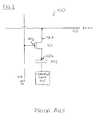
- FIG. 4a circuit diagram of a pump circuit 400 according to one embodiment of the present invention.
- the pump circuit 400includes a source of input power (Vcc) 406 , which is coupled to a resistor 405 .
- the resistoris coupled to an inductor 404 .
- the inductor 404is coupled to the drain of a transistor 403 at node 410 .
- the transistor 403is also coupled to an oscillator 401 via its gate and to a ground potential 402 via its source.
- Node 410is also coupled to a diode 407 , which is also coupled to a holding capacitor 408 and a output node 409 .
- the oscillator 410generates a square wave or pulse train which cyclically switches the transistor 403 on and off.
- current from the voltage source 406flows to the ground potential 402 via resistor 405 , inductor 404 , and transistor 403 .
- Energyis stored in the inductor 404 in the form of an electric field.
- the transistor 403is switched off, the voltage at the inductor 404 , and therefore also at node 410 , increases as the inductor 404 dissipates the stored energy in an attempt to maintain the current flow. This is known as the flyback effect.
- the increased voltagecauses additional charge to be stored in the holding capacitor 408 , thereby presenting a boosted voltage Vccp at the output terminal 409 .
- the electric field within the inductor 404collapses and the voltage at node 410 drops.
- the diode 407prevents current from flowing from the holding capacitor 408 to node 410 , thereby maintaining the boosted voltage Vccp at the output node 409 .
- the pump circuit 400is suitable for use in a high speed semiconductor device.
- the pump circuit 400is integrated into a high speed semiconductor memory device, for example, dynamic random access memory (DRAM), synchronous dynamic random access memory (SDRAM), or advance DRAM technology (ADT) devices.
- the input power sourcemay have a potential of approximately 1.8 volts and be capable of supplying a current of 95 mA. If the inductor has an inductance of 18 nH, the pump circuit 400 would be capable of outputting a boosted voltage Vccp of 2.8 volts while being switched at a frequency of 1 GHz (with transistor 403 having a fall time of 0.5 ns).
- the pump circuit 400is a single phase pump because the pump only produces a boosted voltage on the falling edge of the pulse train generated by the oscillator 401 .
- FIG. 5is a circuit diagram of a dual phase pump 500 , which generates the boosted voltage on both the rising and the falling edges of the pulse train.
- the dual phase pump 500is essentially two of the single phase pump circuits 400 wired to run in parallel.
- an inverter 501is in the circuit path between the oscillator 401 and only one of the two transistors. The addition of the inverter causes the two transistors 403 a , 403 b to operate out of phase.
- the inductor 404is an essential element of the charge pumps 400 , 500 of the present invention.
- One feature of the inductor 404is that it is integrated into the semiconductor device.
- FIG. 6is a more detailed illustration of the inductor 404 .
- the inductor 404is comprised of a plurality of series connected metal spirals 601 .
- Each of the metal spirals 601may be formed, for example, at adjacent locations in the same metal layer.
- a plurality of connectors 602may be used to serially connect the plurality of metal spirals 601 .
- Portions of connectors 602may be formed in different metalization layers and the portions connected with a conductive via.
- a pair of connectors 603which is used to interface the inductor 404 to other components upon the semiconductor device. Portions of connectors 603 may likewise be formed in different metalization layers, with the portions being interconnected with conductive vias.
- the inductance of the inductor 404may be changed by varying the characteristics of each metal spiral 601 .
- the inductance of each metal spiral 602may be changed by varying the width of the metal, the distance between each spiral, or the number of spirals.
- the inductance of the inductor 404may also be changed by varying the number of serially connected spirals.
- FIG. 7is an illustration of how semiconductor memory devices employing charge pumps 400 , 500 of the p resent invention may be used in a computer system.
- the computer system 700includes a central processing unit 701 which is coupled to a local bus 702 .
- High speed peripherals, such as a graphics card 711 , a memory controller 703 and an expansion bus controller 706are also coupled to the local bus 702 .
- the memory controller 703is also coupled to a memory bus 704 .
- the memory bus 704may include memory devices 200 a , 200 b which incorporate the charge pumps 400 , 500 of the present invention.
- FIG. 7is an illustration of how semiconductor memory devices employing charge pumps 400 , 500 of the present invention may be used in a computer system.
- the computer system 700includes a central processing unit 701 which is coupled to a local bus 702 .
- High speed peripherals, such as a graphics card 711 , a memory controller 703 and an expansion bus controller 706are also coupled to the local bus 702
- memory device 200 ainclude s a single phase charge pump 400 while memory device 200 b includes a double phase charge pump 500 .
- the charge pumps 400 , 500are coupled to a power supply 705 via lines 205 , 206 and provide a boosted voltage to the operational circuit 203 of the memory device 200 a , 200 b via line 204 .
- the expansion bus controller 706is also coupled to a expansion bus 707 , to which various peripherals 708 , 709 , 710 may be attached. Examples of peripherals include, but are not limited to keyboards, mice, disk controllers, scanners, etc.
Landscapes
- Engineering & Computer Science (AREA)
- Power Engineering (AREA)
- Microelectronics & Electronic Packaging (AREA)
- Computer Hardware Design (AREA)
- Semiconductor Integrated Circuits (AREA)
- Dc-Dc Converters (AREA)
- Dram (AREA)
Abstract
Description
Claims (20)
Priority Applications (1)
| Application Number | Priority Date | Filing Date | Title |
|---|---|---|---|
| US09/805,207US6538494B2 (en) | 2001-03-14 | 2001-03-14 | Pump circuits using flyback effect from integrated inductance |
Applications Claiming Priority (1)
| Application Number | Priority Date | Filing Date | Title |
|---|---|---|---|
| US09/805,207US6538494B2 (en) | 2001-03-14 | 2001-03-14 | Pump circuits using flyback effect from integrated inductance |
Publications (2)
| Publication Number | Publication Date |
|---|---|
| US20020130699A1 US20020130699A1 (en) | 2002-09-19 |
| US6538494B2true US6538494B2 (en) | 2003-03-25 |
Family
ID=25190949
Family Applications (1)
| Application Number | Title | Priority Date | Filing Date |
|---|---|---|---|
| US09/805,207Expired - LifetimeUS6538494B2 (en) | 2001-03-14 | 2001-03-14 | Pump circuits using flyback effect from integrated inductance |
Country Status (1)
| Country | Link |
|---|---|
| US (1) | US6538494B2 (en) |
Cited By (8)
| Publication number | Priority date | Publication date | Assignee | Title |
|---|---|---|---|---|
| US20030117209A1 (en)* | 2001-12-21 | 2003-06-26 | Fujitsu Limited | Bipolar supply voltage generator and semiconductor device for same |
| US20030123239A1 (en)* | 2002-01-02 | 2003-07-03 | Rabadam Eleanor P. | Lower profile package with power supply in package |
| US20040056704A1 (en)* | 2002-09-25 | 2004-03-25 | Aalami Dean D. | Apparatus for supplying high voltages with low power for solid state detectors and grids |
| US20040252426A1 (en)* | 2003-06-10 | 2004-12-16 | Michael Hargrove | Technique to reduce ESD loading capacitance |
| US20050127983A1 (en)* | 2003-12-11 | 2005-06-16 | Denso Corporation | Voltage booster device having voltage-suppressing circuit |
| US20110012670A1 (en)* | 2002-04-01 | 2011-01-20 | Eskildsen Steven R | Providing in package power supplies for integrated circuits |
| US10141915B2 (en) | 2015-08-07 | 2018-11-27 | International Business Machines Corporation | Sequenced pulse-width adjustment in a resonant clocking circuit |
| US10839918B1 (en)* | 2019-06-24 | 2020-11-17 | Sandisk Technologies Llc | Boost converter in memory chip |
Families Citing this family (3)
| Publication number | Priority date | Publication date | Assignee | Title |
|---|---|---|---|---|
| US10263519B2 (en) | 2015-07-23 | 2019-04-16 | International Business Machines Corporation | Resonant virtual supply booster for synchronous digital circuits having a predictable evaluate time |
| US9612614B2 (en) | 2015-07-31 | 2017-04-04 | International Business Machines Corporation | Pulse-drive resonant clock with on-the-fly mode change |
| US9568548B1 (en) | 2015-10-14 | 2017-02-14 | International Business Machines Corporation | Measurement of signal delays in microprocessor integrated circuits with sub-picosecond accuracy using frequency stepping |
Citations (9)
| Publication number | Priority date | Publication date | Assignee | Title |
|---|---|---|---|---|
| US5126590A (en) | 1991-06-17 | 1992-06-30 | Micron Technology, Inc. | High efficiency charge pump |
| US5267218A (en)* | 1992-03-31 | 1993-11-30 | Intel Corporation | Nonvolatile memory card with a single power supply input |
| US5367489A (en) | 1991-11-07 | 1994-11-22 | Samsung Electronics Co., Ltd. | Voltage pumping circuit for semiconductor memory devices |
| US5721509A (en)* | 1996-02-05 | 1998-02-24 | Motorola, Inc. | Charge pump having reduced threshold voltage losses |
| US5939866A (en)* | 1997-04-10 | 1999-08-17 | Telefonaktiebolaget L M Ericsson | Preregulated DC-to-DC converter |
| US6011743A (en) | 1997-12-17 | 2000-01-04 | Lg Semicon Co., Ltd. | Charge pump circuit for memory device |
| US6091613A (en) | 1998-04-21 | 2000-07-18 | Hyundai Electronics Industries Co., Ltd. | Semiconductor memory device having a multi-step pulse generation circuit |
| US6160440A (en) | 1998-09-25 | 2000-12-12 | Intel Corporation | Scaleable charge pump for use with a low voltage power supply |
| US6160749A (en) | 1997-03-14 | 2000-12-12 | Hyundai Electronics America | Pump control circuit |
- 2001
- 2001-03-14USUS09/805,207patent/US6538494B2/ennot_activeExpired - Lifetime
Patent Citations (9)
| Publication number | Priority date | Publication date | Assignee | Title |
|---|---|---|---|---|
| US5126590A (en) | 1991-06-17 | 1992-06-30 | Micron Technology, Inc. | High efficiency charge pump |
| US5367489A (en) | 1991-11-07 | 1994-11-22 | Samsung Electronics Co., Ltd. | Voltage pumping circuit for semiconductor memory devices |
| US5267218A (en)* | 1992-03-31 | 1993-11-30 | Intel Corporation | Nonvolatile memory card with a single power supply input |
| US5721509A (en)* | 1996-02-05 | 1998-02-24 | Motorola, Inc. | Charge pump having reduced threshold voltage losses |
| US6160749A (en) | 1997-03-14 | 2000-12-12 | Hyundai Electronics America | Pump control circuit |
| US5939866A (en)* | 1997-04-10 | 1999-08-17 | Telefonaktiebolaget L M Ericsson | Preregulated DC-to-DC converter |
| US6011743A (en) | 1997-12-17 | 2000-01-04 | Lg Semicon Co., Ltd. | Charge pump circuit for memory device |
| US6091613A (en) | 1998-04-21 | 2000-07-18 | Hyundai Electronics Industries Co., Ltd. | Semiconductor memory device having a multi-step pulse generation circuit |
| US6160440A (en) | 1998-09-25 | 2000-12-12 | Intel Corporation | Scaleable charge pump for use with a low voltage power supply |
Non-Patent Citations (5)
| Title |
|---|
| 28V, Low-Power, High Voltage, Boost or Inverting DC-DC Converter. |
| Arcioni et al., "Design and Characterization of Si Integrated Inductors", IEEE Instumentation and Measurement Technology Conference, 5/98. |
| Brent Keeth, "A DRAM Circuit Design Tutorial", Micron Technology, Inc., 12/95, pp. 75-79. |
| Chap. 1, An Introduction to DRAM, Sec. 1.2 DRAM Basics, pp. 24-29. |
| Chap. 6, Voltage Converters, Sec. 6.2 Pumps and Generators, pp. 166-171. |
Cited By (12)
| Publication number | Priority date | Publication date | Assignee | Title |
|---|---|---|---|---|
| US20030117209A1 (en)* | 2001-12-21 | 2003-06-26 | Fujitsu Limited | Bipolar supply voltage generator and semiconductor device for same |
| US7342436B2 (en)* | 2001-12-21 | 2008-03-11 | Fujitsu Limited | Bipolar supply voltage generator and semiconductor device for same |
| US20030123239A1 (en)* | 2002-01-02 | 2003-07-03 | Rabadam Eleanor P. | Lower profile package with power supply in package |
| US6812566B2 (en)* | 2002-01-02 | 2004-11-02 | Intel Corporation | Lower profile package with power supply in package |
| US20110012670A1 (en)* | 2002-04-01 | 2011-01-20 | Eskildsen Steven R | Providing in package power supplies for integrated circuits |
| US20040056704A1 (en)* | 2002-09-25 | 2004-03-25 | Aalami Dean D. | Apparatus for supplying high voltages with low power for solid state detectors and grids |
| US20040252426A1 (en)* | 2003-06-10 | 2004-12-16 | Michael Hargrove | Technique to reduce ESD loading capacitance |
| US7315438B2 (en)* | 2003-06-10 | 2008-01-01 | Seiko Epson Corporation | Technique to reduce ESD loading capacitance |
| US20050127983A1 (en)* | 2003-12-11 | 2005-06-16 | Denso Corporation | Voltage booster device having voltage-suppressing circuit |
| US7167040B2 (en)* | 2003-12-11 | 2007-01-23 | Denso Corporation | Voltage booster device having voltage-suppressing circuit |
| US10141915B2 (en) | 2015-08-07 | 2018-11-27 | International Business Machines Corporation | Sequenced pulse-width adjustment in a resonant clocking circuit |
| US10839918B1 (en)* | 2019-06-24 | 2020-11-17 | Sandisk Technologies Llc | Boost converter in memory chip |
Also Published As
| Publication number | Publication date |
|---|---|
| US20020130699A1 (en) | 2002-09-19 |
Similar Documents
| Publication | Publication Date | Title |
|---|---|---|
| US7521978B2 (en) | Clock driver | |
| US8154333B2 (en) | Charge pump circuits, systems, and operational methods thereof | |
| US7023260B2 (en) | Charge pump circuit incorporating corresponding parallel charge pump stages and method therefor | |
| US5343088A (en) | Charge pump circuit for a substrate voltage generator of a semiconductor memory device | |
| US20020071318A1 (en) | Semiconductor device | |
| US6373315B2 (en) | Signal potential conversion circuit | |
| US7710193B2 (en) | High voltage generator and word line driving high voltage generator of memory device | |
| TW200832877A (en) | A new charge pump circuit for high voltage generation | |
| US6326834B1 (en) | Pump circuit boosting a supply voltage | |
| US6538494B2 (en) | Pump circuits using flyback effect from integrated inductance | |
| JPH07326957A (en) | Cmos circuit | |
| US7365591B2 (en) | Voltage generating circuit | |
| US5774012A (en) | Charge-pumping circuit for semiconductor memory device | |
| US7800958B2 (en) | Voltage generating unit of semiconductor memory device | |
| US5638013A (en) | Charge redistribution circuit and method | |
| US6240025B1 (en) | Voltage generator | |
| KR100282082B1 (en) | Word line driver circuit | |
| US7710795B2 (en) | Semiconductor memory device | |
| US9379605B2 (en) | Clocking circuit, charge pumps, and related methods of operation | |
| US20110115551A1 (en) | Charge pump utilizing external clock signal | |
| US6653889B2 (en) | Voltage generating circuits and methods including shared capacitors | |
| JP2848796B2 (en) | Signal transmission method | |
| JPH1069796A (en) | Semiconductor integrated circuit with high-speed test function | |
| JP2972723B2 (en) | Semiconductor integrated circuit | |
| US7276959B2 (en) | Pumping circuit of semiconductor device |
Legal Events
| Date | Code | Title | Description |
|---|---|---|---|
| AS | Assignment | Owner name:MICRON TECHNOLOGY, INC., IDAHO Free format text:ASSIGNMENT OF ASSIGNORS INTEREST;ASSIGNOR:ZIMLICH, DAVID A.;REEL/FRAME:011599/0742 Effective date:20010309 | |
| STCF | Information on status: patent grant | Free format text:PATENTED CASE | |
| FPAY | Fee payment | Year of fee payment:4 | |
| FEPP | Fee payment procedure | Free format text:PAYOR NUMBER ASSIGNED (ORIGINAL EVENT CODE: ASPN); ENTITY STATUS OF PATENT OWNER: LARGE ENTITY Free format text:PAYER NUMBER DE-ASSIGNED (ORIGINAL EVENT CODE: RMPN); ENTITY STATUS OF PATENT OWNER: LARGE ENTITY | |
| FPAY | Fee payment | Year of fee payment:8 | |
| FPAY | Fee payment | Year of fee payment:12 | |
| AS | Assignment | Owner name:U.S. BANK NATIONAL ASSOCIATION, AS COLLATERAL AGENT, CALIFORNIA Free format text:SECURITY INTEREST;ASSIGNOR:MICRON TECHNOLOGY, INC.;REEL/FRAME:038669/0001 Effective date:20160426 Owner name:U.S. BANK NATIONAL ASSOCIATION, AS COLLATERAL AGEN Free format text:SECURITY INTEREST;ASSIGNOR:MICRON TECHNOLOGY, INC.;REEL/FRAME:038669/0001 Effective date:20160426 | |
| AS | Assignment | Owner name:MORGAN STANLEY SENIOR FUNDING, INC., AS COLLATERAL AGENT, MARYLAND Free format text:PATENT SECURITY AGREEMENT;ASSIGNOR:MICRON TECHNOLOGY, INC.;REEL/FRAME:038954/0001 Effective date:20160426 Owner name:MORGAN STANLEY SENIOR FUNDING, INC., AS COLLATERAL Free format text:PATENT SECURITY AGREEMENT;ASSIGNOR:MICRON TECHNOLOGY, INC.;REEL/FRAME:038954/0001 Effective date:20160426 | |
| AS | Assignment | Owner name:U.S. BANK NATIONAL ASSOCIATION, AS COLLATERAL AGENT, CALIFORNIA Free format text:CORRECTIVE ASSIGNMENT TO CORRECT THE REPLACE ERRONEOUSLY FILED PATENT #7358718 WITH THE CORRECT PATENT #7358178 PREVIOUSLY RECORDED ON REEL 038669 FRAME 0001. ASSIGNOR(S) HEREBY CONFIRMS THE SECURITY INTEREST;ASSIGNOR:MICRON TECHNOLOGY, INC.;REEL/FRAME:043079/0001 Effective date:20160426 Owner name:U.S. BANK NATIONAL ASSOCIATION, AS COLLATERAL AGEN Free format text:CORRECTIVE ASSIGNMENT TO CORRECT THE REPLACE ERRONEOUSLY FILED PATENT #7358718 WITH THE CORRECT PATENT #7358178 PREVIOUSLY RECORDED ON REEL 038669 FRAME 0001. ASSIGNOR(S) HEREBY CONFIRMS THE SECURITY INTEREST;ASSIGNOR:MICRON TECHNOLOGY, INC.;REEL/FRAME:043079/0001 Effective date:20160426 | |
| AS | Assignment | Owner name:JPMORGAN CHASE BANK, N.A., AS COLLATERAL AGENT, ILLINOIS Free format text:SECURITY INTEREST;ASSIGNORS:MICRON TECHNOLOGY, INC.;MICRON SEMICONDUCTOR PRODUCTS, INC.;REEL/FRAME:047540/0001 Effective date:20180703 Owner name:JPMORGAN CHASE BANK, N.A., AS COLLATERAL AGENT, IL Free format text:SECURITY INTEREST;ASSIGNORS:MICRON TECHNOLOGY, INC.;MICRON SEMICONDUCTOR PRODUCTS, INC.;REEL/FRAME:047540/0001 Effective date:20180703 | |
| AS | Assignment | Owner name:MICRON TECHNOLOGY, INC., IDAHO Free format text:RELEASE BY SECURED PARTY;ASSIGNOR:U.S. BANK NATIONAL ASSOCIATION, AS COLLATERAL AGENT;REEL/FRAME:047243/0001 Effective date:20180629 | |
| AS | Assignment | Owner name:MICRON TECHNOLOGY, INC., IDAHO Free format text:RELEASE BY SECURED PARTY;ASSIGNOR:MORGAN STANLEY SENIOR FUNDING, INC., AS COLLATERAL AGENT;REEL/FRAME:050937/0001 Effective date:20190731 | |
| AS | Assignment | Owner name:MICRON TECHNOLOGY, INC., IDAHO Free format text:RELEASE BY SECURED PARTY;ASSIGNOR:JPMORGAN CHASE BANK, N.A., AS COLLATERAL AGENT;REEL/FRAME:051028/0001 Effective date:20190731 Owner name:MICRON SEMICONDUCTOR PRODUCTS, INC., IDAHO Free format text:RELEASE BY SECURED PARTY;ASSIGNOR:JPMORGAN CHASE BANK, N.A., AS COLLATERAL AGENT;REEL/FRAME:051028/0001 Effective date:20190731 |