US6538270B1 - Staggered bitline strapping of a non-volatile memory cell - Google Patents
Staggered bitline strapping of a non-volatile memory cellDownload PDFInfo
- Publication number
- US6538270B1 US6538270B1US09/721,031US72103100AUS6538270B1US 6538270 B1US6538270 B1US 6538270B1US 72103100 AUS72103100 AUS 72103100AUS 6538270 B1US6538270 B1US 6538270B1
- Authority
- US
- United States
- Prior art keywords
- memory cells
- array
- bitline
- contacts
- bitlines
- Prior art date
- Legal status (The legal status is an assumption and is not a legal conclusion. Google has not performed a legal analysis and makes no representation as to the accuracy of the status listed.)
- Expired - Lifetime
Links
Images


Classifications
- H—ELECTRICITY
- H10—SEMICONDUCTOR DEVICES; ELECTRIC SOLID-STATE DEVICES NOT OTHERWISE PROVIDED FOR
- H10B—ELECTRONIC MEMORY DEVICES
- H10B43/00—EEPROM devices comprising charge-trapping gate insulators
- H10B43/30—EEPROM devices comprising charge-trapping gate insulators characterised by the memory core region
- H—ELECTRICITY
- H10—SEMICONDUCTOR DEVICES; ELECTRIC SOLID-STATE DEVICES NOT OTHERWISE PROVIDED FOR
- H10B—ELECTRONIC MEMORY DEVICES
- H10B69/00—Erasable-and-programmable ROM [EPROM] devices not provided for in groups H10B41/00 - H10B63/00, e.g. ultraviolet erasable-and-programmable ROM [UVEPROM] devices
Definitions
- the present inventionrelates to the field of non-volatile memory devices. More particularly, the invention relates to a multi-bit flash electrically erasable programmable read only memory (EEPROM) cell with a bitline.
- EEPROMelectrically erasable programmable read only memory
- Non-volatile semiconductor memoryincludes read only memory (ROM), programmable read only memory (PROM), erasable programmable read only memory (EPROM), electrically erasable programmable read only memory (EEPROM) and flash EEPROM.
- ROMread only memory
- PROMprogrammable read only memory
- EPROMerasable programmable read only memory
- EEPROMelectrically erasable programmable read only memory
- flash EEPROMflash EEPROM
- Flash EEPROMsare similar to EEPROMs in that memory cells can be programmed (i.e., written) and erased electrically but with the additional ability of erasing all memory cells at once, hence the term flash EEPROM.
- Oxide-Nitrogen-Oxide (ONO) EEPROM deviceAn example of a single transistor Oxide-Nitrogen-Oxide (ONO) EEPROM device is disclosed in the technical article entitled “A True Single-Transistor Oxide-Nitride-Oxide EEPROM Device,” T. Y. Chan, K. K. Young and Chenming Hu, IEEE Electron Device Letters, March 1987.
- the memory cellis programmed by hot electron injection and the injected charges are stored in the oxide-nitride-oxide (ONO) layer of the device.
- ONO EEPROM devicesare disclosed in U.S. Pat. Nos. 5,635,415; 5,768,192 and PCT patent application publication WO 99/07000, the contents of each reference are hereby incorporated herein by reference.
- an NROM cell 100included a grid of polygates or word lines 102 and buried bitlines 104 .
- the bitlines 104were formed in the N+ region of the substrate so that a higher density of bitlines can be formed that region versus when the bitlines were formed in a metal layer.
- Select transistors 106were required to be placed every N or N/2 polygates 102 , where N is the number of polygates between contacts 108 . This in the past has required a select transistor 106 being required every 16 or 32 cells in order to reduce the bitline to cell resistance.
- the bitline resistance in the N+ regionlimits the number of cells between select transistors.
- contacts associated with the cellmust be spaced from the polysilicon of the gate. As feature sizes are reduced according to integrated circuit processes, smaller dimensions are required to achieve higher packing densities. Generally, contacts must be spaced apart from the stacked gate so alignment errors do not result in a shorting of the stacked gate with the source contact or the drain contact. The spacing between the contact and gate contributes to the overall size of the flash memory cell.
- One aspect of the inventionregards an array of memory cells that includes a plurality of memory cells interconnected via a grid of wordlines and bitlines, wherein each of the bitlines is buried.
- a strapconnects one of the buried bitlines to a gate that underlies one of the plurality of contacts and wherein a column of the bitlines has a first discontinuous and a second discontinuous bitline that are separated from one another by a distance ⁇ .
- the above aspect of the present inventionprovides the advantage of reducing the source plus drain resistance per cell.
- the above aspect of the present inventionprovides the advantage of eliminating the need for select transistors and reducing the total size of an array.
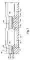
- FIG. 1illustrates a top cross-sectional view of a prior art NROM cell with a buried bit line
- FIGS. 2-6illustrate side cross-sectional views of processing steps to form an embodiment of the present invention
- FIG. 7illustrates a side cross-sectional view of a two-bit flash EEPROM cell constructed in accordance with an embodiment of the present invention utilizing the process of FIGS. 2-6;
- FIG. 8illustrates a top cross-sectional view of the two bit flash EEPROM cell of FIG. 7.
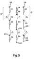
- FIG. 9illustrates a top cross-sectional view of a second embodiment of a two-bit flash EEPROM cell according to the present invention.
- Non-volatile memory designershave taken advantage of the ability of silicon nitride to store charge in localized regions and have designed memory circuits that utilize two regions of stored charge within the ONO layer.
- This type of non-volatile memory deviceis known as a two-bit EEPROM.
- the two-bit EEPROMis capable of storing twice as much information as a conventional EEPROM in a memory array of equal size.
- a left and right bitis stored in physically different areas of the silicon nitride layer, near left and right regions of each memory cell. Programming methods are then used that enable two-bits to be programmed and read simultaneously.
- the two-bits of the memory cellcan be individually erased by applying suitable erase voltages to the gate and to either the source or drain regions.
- Two bit memory cellsare typically accessed by buried bit-lines formed in a semiconductor substrate.
- a bit-line oxide layeris formed over the buried bit-line prior to forming a central gate electrode.
- FIG. 2Shown in FIG. 2, in cross-section is a portion of a semiconductor substrate 200 having already undergone several processing steps.
- An ONO layer 202overlies the semiconductor substrate 200 and includes a first oxide layer 206 , a second oxide layer 208 and a silicon nitride layer 210 sandwiched between the first oxide layer 206 and the second oxide layer 208 .
- Resist layer 212is formed to overly the ONO layer 202 .
- Resist layer 212can be one of a number of different types of resist, including optical photoresist responsive to visible and near UV light, deep UV resist and the like.
- resist layer 212can be an inorganic resist layer, an X-ray resist layer and the like.
- resist layer 212is a Novolak resin photoresist material.
- Resist layer 212is exposed to radiation of the appropriate wavelength and developed to form a resist pattern overlying ONO layer 202 , as illustrated in FIG. 3 .
- Resist pattern 212is formed to have a predetermined geometric configuration for the fabrication of buried bit-line regions in semiconductor substrate 200 . Resist pattern 212 allows for exposing selected regions 216 of semiconductor substrate 200 .
- an implantation processis carried out to form pocket regions 218 , 220 in semiconductor substrate 200 .
- Pocket regions 218 , 220are preferably formed by an angled ion implant process in which semiconductor substrate 200 is held at an angle of about 7° to about 60°, typically 30° to 45°, with respect to normal during the ion implantation process.
- the angled ion implant processforms pocket regions 218 , 220 in semiconductor substrate 200 in locations that partially underlie a portion of resist pattern 212 .
- a p-type dopantsuch as boron
- boronis ion implanted into semiconductor substrate 200 to form pocket regions 218 , 220 .
- the boron ionspenetrate ONO layer 202 and enter semiconductor substrate 200 at an angle sufficient to create a boron pocket region that extends partially beneath resist pattern 212 .
- portions of ONO layer 202 exposed by resist pattern 212are etched to expose principal surface 222 of semiconductor substrate 200 .
- resist pattern 212is used as an etching mask, such that the etching process exposes principal surface 212 in selected regions 216 defined by resist mask 212 .
- ONO layer 202is anisotropically etched, such that ONO layer 202 and resist pattern 212 have continuous, substantially vertical sidewalls.
- an ion implantation processis carried out to form a buried bit-line region 224 in selected region 216 of semiconductor substrate 200 .
- an n-type dopantsuch as arsenic
- buried bit-line region 224is formed by the ion implantation of arsenic using a dose of about 3 ⁇ 10 15 to about 5 ⁇ 10 15 ions per square centimeter. The ion implantation energy is selected so as to form buried bit-line region 224 to a selected junction depth in semiconductor substrate 200 .
- the ion implantation energyis of sufficient magnitude, such that the junction depth of buried bit-line region 224 is greater than the junction depth of pocket regions 218 , 220 .
- junction depthrefers to the distance from the surface of the substrate to the deepest point of formation of a p/n junction associated with the implanted region within the substrate.
- the order of formation of the pocket regions 218 , 220 and the buried bit-line region 224can be reversed from that described above.
- an implant processcan be carried out to form bit-line region 224 , followed by an angled implant process to form pocket regions 218 , 220 .
- ONO layer 202can be etched before either implant process is carried out.
- bit-line oxide layer 226is formed by thermal oxidation of semiconductor substrate 200 using ONO layer 202 as an oxidation mask.
- ONO layer 202having been previously patterned by the etching process described above, exposes selected regions 216 of semiconductor substrate 200 .
- the patterned portions of ONO layer 202prevent the oxidation of semiconductor substrate 200 in region underlying ONO layer 202 .
- bit-line oxide layers 226are confined to selected regions 216 of semiconductor substrate 200 .
- bitline layers 226overly buried bit-line regions 224 in semiconductor substrate 200 .
- control gate electrode contacts/electrodes 228are formed over the floating gate electrodes 229 by depositing a layer of polycrystalline silicon by a CVD process, followed by patterning and etching to form thin control-gate lines overlying the substrate 200 . As shown in FIG. 6, the electrode 228 overlies the layers 226 and bit line oxide regions 224 .
- the flash EEPROM memory cellincludes an N+ type substrate 200 having two buried PN junctions, one being between the source pocket 218 and substrate 200 , termed the left junction and the other being between the drain pocket 220 and the substrate 200 , termed the right junction.
- Above the channel 230is an oxide layer 206 made of silicon dioxide.
- the oxide layer 206has a thickness that is less than or equal to 60 Angstroms, and which forms an electrical isolation layer over the channel.
- a charge trapping layer 210On top of the oxide layer 206 is a charge trapping layer 210 that has a thickness ranging from approximately 20 to 100 Angstroms and preferably is comprised of silicon nitride, Si 3 N 4 . The hot electrons are trapped as they are injected into the charge trapping layer so that the charge trapping layer serves as the memory retention layer.
- the thickness of layer 210is chosen to be in excess of approximately 50 Angstroms to prevent electrons from tunneling through the layer 206 and leaving charge trapping layer 210 during the operation of the cell.
- the lifetime of the cell of this inventionis greatly extended relative to prior art NMOS devices.
- the memory cellis capable of storing two bits of data, a right bit and a left bit.
- the two-bit memory cellis a symmetrical device.
- the left junctionserves as the source terminal and the right junction serves as the drain terminal for the right bit.
- the right junctionserves as the source terminal and the left junction serves as the drain terminal.
- the terms left, or first junction and right or second junctionare used herein rather than source and drain.
- source and drainare utilized. However, it should be understood that the source and drain terminals for the second bit are reversed compared to the source and drain terminals for the first bit.
- a layer of silicon dioxide 208is formed over the charge trapping layer, (i.e., silicon nitride layer), and has a thickness that ranges between approximately 60 to 100 Angstroms.
- the silicon dioxide layer 208functions to electrically isolate a conductive gate 228 formed over the silicon dioxide layer 208 from charge trapping layer 210 .
- the thickness of gate 228is approximately 4,000 Angstroms.
- Gate 228is constructed from an N-type material, such as polycrystalline silicon that is typically heavily doped with an N-type impurity such as phosphorous in the 10 19 to 10 20 atom/cc range.
- polysilicon straps 230can be made concurrently with or without bitlines 226 and are used to connect each buried bitline 224 to the overlying gate electrode 228 .
- the bitlines 224are formed to be discontinuous and broken.
- the bitlines A 1 , A 2 and A 3are aligned along a column and are separated from one another by a distance ⁇ that constitutes a constant number of cells.
- the contacts 228 associated with each bitline A 1 , A 2 , and A 3are positioned in the middle of the bitline. Furthermore, the contacts 228 are separated by a distance D from one another by a constant number of cells.
- the separation between contacts 228is the same for each column of bitlines.
- the contacts 228are staggered or offset so that contacts 228 on adjacent bitlines are not adjacent to each other and where each contact 228 overlies a buried bitline 224 .
- the offset distance ODis equal to one half of the separation distance D.
- the contacts 228are positioned along wordlines associated with polygates 229 .
- FIG. 9An alternative embodiment of the array of memory cells is shown in FIG. 9 .
- the bitlines A 1 , A 2 and A 3are aligned along a column and are separated from one another by a distance ⁇ that constitutes a constant number of cells.
- the discontinuous bitlines of adjacent columnsare not staggered relative to one another as in FIG. 8 .
- the contacts 228are located at the ends of the discontinuous bitlines. The end of the bitline that the contacts 228 are located is the same for each column of bitlines, where adjacent columns of bitlines have the contacts 228 located at different ends of the bitlines as shown in FIG. 9 . This produces a staggered pattern of contacts 228 .
- the contacts 228are separated by a distance D from one another by a constant number of cells.
- the separation between contacts 228is the same for each column of bitlines.
- the contacts 228are staggered or offset so that contacts 228 on adjacent bitlines are not adjacent to each other and where each contact 228 overlies a buried bitline 224 .
- the offset distance ODis equal to the separation distance ⁇ .
- the contacts 228are positioned along wordlines associated with polygates 229 . As with the embodiment of FIG. 8, breaking up the bitlines in each column and having staggered contacts, the source plus drain resistance per cell can be maintained constant without the need for select transistors. The elimination of select transistors reduces the total size of the memory array when compared with the array of FIG. 1 .
- the channel lengthsbecome shorter and short channel effects take hold.
- short channel effectsmay become prevalent sooner than in the case of the single bit transistor.
- the two-bit transistormay need to be scaled by a smaller factor.
Landscapes
- Semiconductor Memories (AREA)
- Non-Volatile Memory (AREA)
Abstract
Description
Claims (22)
Priority Applications (3)
| Application Number | Priority Date | Filing Date | Title |
|---|---|---|---|
| US09/721,031US6538270B1 (en) | 2000-05-16 | 2000-11-22 | Staggered bitline strapping of a non-volatile memory cell |
| AU2001255791AAU2001255791A1 (en) | 2000-05-16 | 2001-05-01 | Staggered bitline strapping of a non-volatile memory cell |
| PCT/US2001/014130WO2001088986A2 (en) | 2000-05-16 | 2001-05-01 | Staggered bitline strapping of a non-volatile memory cell |
Applications Claiming Priority (2)
| Application Number | Priority Date | Filing Date | Title |
|---|---|---|---|
| US20440600P | 2000-05-16 | 2000-05-16 | |
| US09/721,031US6538270B1 (en) | 2000-05-16 | 2000-11-22 | Staggered bitline strapping of a non-volatile memory cell |
Publications (1)
| Publication Number | Publication Date |
|---|---|
| US6538270B1true US6538270B1 (en) | 2003-03-25 |
Family
ID=26899449
Family Applications (1)
| Application Number | Title | Priority Date | Filing Date |
|---|---|---|---|
| US09/721,031Expired - LifetimeUS6538270B1 (en) | 2000-05-16 | 2000-11-22 | Staggered bitline strapping of a non-volatile memory cell |
Country Status (3)
| Country | Link |
|---|---|
| US (1) | US6538270B1 (en) |
| AU (1) | AU2001255791A1 (en) |
| WO (1) | WO2001088986A2 (en) |
Cited By (38)
| Publication number | Priority date | Publication date | Assignee | Title |
|---|---|---|---|---|
| US20020197797A1 (en)* | 2000-11-17 | 2002-12-26 | Noboru Egawa | Non-volatile read only memory and its manufacturing method |
| US20030039153A1 (en)* | 2001-01-18 | 2003-02-27 | Eduardo Maayan | EEPROM array and method for operation thereof |
| US6649971B1 (en)* | 2002-08-28 | 2003-11-18 | Macronix International Co., Ltd. | Nitride read-only memory cell for improving second-bit effect and method for making thereof |
| US20040008541A1 (en)* | 2002-07-10 | 2004-01-15 | Eduardo Maayan | Multiple use memory chip |
| US20040097045A1 (en)* | 2002-11-15 | 2004-05-20 | Cheng-Jye Liu | Method for fabricating nitride read-only memory |
| US20060036803A1 (en)* | 2004-08-16 | 2006-02-16 | Mori Edan | Non-volatile memory device controlled by a micro-controller |
| US20070048936A1 (en)* | 2005-08-31 | 2007-03-01 | Jongoh Kim | Method for forming memory cell and periphery circuits |
| US20070070678A1 (en)* | 2005-09-28 | 2007-03-29 | Fujitsu Limited | Semiconductor storage device |
| US7221138B2 (en) | 2005-09-27 | 2007-05-22 | Saifun Semiconductors Ltd | Method and apparatus for measuring charge pump output current |
| US20070255889A1 (en)* | 2006-03-22 | 2007-11-01 | Yoav Yogev | Non-volatile memory device and method of operating the device |
| US7317633B2 (en) | 2004-07-06 | 2008-01-08 | Saifun Semiconductors Ltd | Protection of NROM devices from charge damage |
| US7352627B2 (en) | 2006-01-03 | 2008-04-01 | Saifon Semiconductors Ltd. | Method, system, and circuit for operating a non-volatile memory array |
| US7369440B2 (en) | 2005-01-19 | 2008-05-06 | Saifun Semiconductors Ltd. | Method, circuit and systems for erasing one or more non-volatile memory cells |
| US7405969B2 (en) | 1997-08-01 | 2008-07-29 | Saifun Semiconductors Ltd. | Non-volatile memory cell and non-volatile memory devices |
| US7420848B2 (en) | 2002-01-31 | 2008-09-02 | Saifun Semiconductors Ltd. | Method, system, and circuit for operating a non-volatile memory array |
| US20080239599A1 (en)* | 2007-04-01 | 2008-10-02 | Yehuda Yizraeli | Clamping Voltage Events Such As ESD |
| US7457183B2 (en) | 2003-09-16 | 2008-11-25 | Saifun Semiconductors Ltd. | Operating array cells with matched reference cells |
| US7466594B2 (en) | 2004-08-12 | 2008-12-16 | Saifun Semiconductors Ltd. | Dynamic matching of signal path and reference path for sensing |
| US7512009B2 (en) | 2001-04-05 | 2009-03-31 | Saifun Semiconductors Ltd. | Method for programming a reference cell |
| CN100485906C (en)* | 2005-09-07 | 2009-05-06 | 旺宏电子股份有限公司 | Method for forming memory cell and peripheral circuit |
| US7532529B2 (en) | 2004-03-29 | 2009-05-12 | Saifun Semiconductors Ltd. | Apparatus and methods for multi-level sensing in a memory array |
| US7535765B2 (en) | 2004-12-09 | 2009-05-19 | Saifun Semiconductors Ltd. | Non-volatile memory device and method for reading cells |
| US7590001B2 (en) | 2007-12-18 | 2009-09-15 | Saifun Semiconductors Ltd. | Flash memory with optimized write sector spares |
| US7605579B2 (en) | 2006-09-18 | 2009-10-20 | Saifun Semiconductors Ltd. | Measuring and controlling current consumption and output current of charge pumps |
| US7638850B2 (en) | 2004-10-14 | 2009-12-29 | Saifun Semiconductors Ltd. | Non-volatile memory structure and method of fabrication |
| US7638835B2 (en) | 2006-02-28 | 2009-12-29 | Saifun Semiconductors Ltd. | Double density NROM with nitride strips (DDNS) |
| US7668017B2 (en) | 2005-08-17 | 2010-02-23 | Saifun Semiconductors Ltd. | Method of erasing non-volatile memory cells |
| US7675782B2 (en) | 2002-10-29 | 2010-03-09 | Saifun Semiconductors Ltd. | Method, system and circuit for programming a non-volatile memory array |
| US7692961B2 (en) | 2006-02-21 | 2010-04-06 | Saifun Semiconductors Ltd. | Method, circuit and device for disturb-control of programming nonvolatile memory cells by hot-hole injection (HHI) and by channel hot-electron (CHE) injection |
| US7701779B2 (en) | 2006-04-27 | 2010-04-20 | Sajfun Semiconductors Ltd. | Method for programming a reference cell |
| US7743230B2 (en) | 2003-01-31 | 2010-06-22 | Saifun Semiconductors Ltd. | Memory array programming circuit and a method for using the circuit |
| US7760554B2 (en) | 2006-02-21 | 2010-07-20 | Saifun Semiconductors Ltd. | NROM non-volatile memory and mode of operation |
| US7786512B2 (en) | 2005-07-18 | 2010-08-31 | Saifun Semiconductors Ltd. | Dense non-volatile memory array and method of fabrication |
| US7808818B2 (en) | 2006-01-12 | 2010-10-05 | Saifun Semiconductors Ltd. | Secondary injection for NROM |
| US20110169069A1 (en)* | 2008-12-22 | 2011-07-14 | Spansion, Llc | Hto offset and bl trench process for memory device to improve device performance |
| US8053812B2 (en) | 2005-03-17 | 2011-11-08 | Spansion Israel Ltd | Contact in planar NROM technology |
| US8253452B2 (en) | 2006-02-21 | 2012-08-28 | Spansion Israel Ltd | Circuit and method for powering up an integrated circuit and an integrated circuit utilizing same |
| US20130235654A1 (en)* | 2012-03-07 | 2013-09-12 | Micron Technology, Inc. | Method, system, and device for base contact layout, such as for memory |
Families Citing this family (1)
| Publication number | Priority date | Publication date | Assignee | Title |
|---|---|---|---|---|
| US6479348B1 (en)* | 2002-03-27 | 2002-11-12 | Advanced Micro Devices, Inc. | Method of making memory wordline hard mask extension |
Citations (13)
| Publication number | Priority date | Publication date | Assignee | Title |
|---|---|---|---|---|
| US5156991A (en)* | 1988-02-05 | 1992-10-20 | Texas Instruments Incorporated | Fabricating an electrically-erasable, electrically-programmable read-only memory having a tunnel window insulator and thick oxide isolation between wordlines |
| US5168334A (en) | 1987-07-31 | 1992-12-01 | Texas Instruments, Incorporated | Non-volatile semiconductor memory |
| US5576567A (en)* | 1990-06-28 | 1996-11-19 | Texas Instruments Incorporated | Vertical memory cell array and method of fabrication |
| US5621697A (en)* | 1995-06-23 | 1997-04-15 | Macronix International Co., Ltd. | High density integrated circuit with bank select structure |
| US5768192A (en)* | 1996-07-23 | 1998-06-16 | Saifun Semiconductors, Ltd. | Non-volatile semiconductor memory cell utilizing asymmetrical charge trapping |
| US5801076A (en)* | 1995-02-21 | 1998-09-01 | Advanced Micro Devices, Inc. | Method of making non-volatile memory device having a floating gate with enhanced charge retention |
| WO1999060631A1 (en) | 1998-05-20 | 1999-11-25 | Saifun Semiconductors Ltd. | Nrom cell with improved programming, erasing and cycling |
| US6064592A (en) | 1998-03-16 | 2000-05-16 | Nec Corporation | Non-volatile semiconductor memory featuring effective cell area reduction using contactless technology |
| US6091094A (en)* | 1998-06-11 | 2000-07-18 | Siemens Aktiengesellschaft | Vertical device formed adjacent to a wordline sidewall and method for semiconductor chips |
| US6130140A (en)* | 1994-07-14 | 2000-10-10 | Micron Technology, Inc. | Method of forming an isolation structure in a semiconductor device |
| US6211548B1 (en)* | 1996-10-25 | 2001-04-03 | Yueh Yale Ma | Metal-gate non-volatile memory cell |
| US6243293B1 (en)* | 1992-01-29 | 2001-06-05 | Interuniversitair Micro-Elektronica Centrum | Contacted cell array configuration for erasable and programmable semiconductor memories |
| US6275414B1 (en)* | 2000-05-16 | 2001-08-14 | Advanced Micro Devices, Inc. | Uniform bitline strapping of a non-volatile memory cell |
- 2000
- 2000-11-22USUS09/721,031patent/US6538270B1/ennot_activeExpired - Lifetime
- 2001
- 2001-05-01AUAU2001255791Apatent/AU2001255791A1/ennot_activeAbandoned
- 2001-05-01WOPCT/US2001/014130patent/WO2001088986A2/enactiveApplication Filing
Patent Citations (13)
| Publication number | Priority date | Publication date | Assignee | Title |
|---|---|---|---|---|
| US5168334A (en) | 1987-07-31 | 1992-12-01 | Texas Instruments, Incorporated | Non-volatile semiconductor memory |
| US5156991A (en)* | 1988-02-05 | 1992-10-20 | Texas Instruments Incorporated | Fabricating an electrically-erasable, electrically-programmable read-only memory having a tunnel window insulator and thick oxide isolation between wordlines |
| US5576567A (en)* | 1990-06-28 | 1996-11-19 | Texas Instruments Incorporated | Vertical memory cell array and method of fabrication |
| US6243293B1 (en)* | 1992-01-29 | 2001-06-05 | Interuniversitair Micro-Elektronica Centrum | Contacted cell array configuration for erasable and programmable semiconductor memories |
| US6130140A (en)* | 1994-07-14 | 2000-10-10 | Micron Technology, Inc. | Method of forming an isolation structure in a semiconductor device |
| US5801076A (en)* | 1995-02-21 | 1998-09-01 | Advanced Micro Devices, Inc. | Method of making non-volatile memory device having a floating gate with enhanced charge retention |
| US5621697A (en)* | 1995-06-23 | 1997-04-15 | Macronix International Co., Ltd. | High density integrated circuit with bank select structure |
| US5768192A (en)* | 1996-07-23 | 1998-06-16 | Saifun Semiconductors, Ltd. | Non-volatile semiconductor memory cell utilizing asymmetrical charge trapping |
| US6211548B1 (en)* | 1996-10-25 | 2001-04-03 | Yueh Yale Ma | Metal-gate non-volatile memory cell |
| US6064592A (en) | 1998-03-16 | 2000-05-16 | Nec Corporation | Non-volatile semiconductor memory featuring effective cell area reduction using contactless technology |
| WO1999060631A1 (en) | 1998-05-20 | 1999-11-25 | Saifun Semiconductors Ltd. | Nrom cell with improved programming, erasing and cycling |
| US6091094A (en)* | 1998-06-11 | 2000-07-18 | Siemens Aktiengesellschaft | Vertical device formed adjacent to a wordline sidewall and method for semiconductor chips |
| US6275414B1 (en)* | 2000-05-16 | 2001-08-14 | Advanced Micro Devices, Inc. | Uniform bitline strapping of a non-volatile memory cell |
Cited By (50)
| Publication number | Priority date | Publication date | Assignee | Title |
|---|---|---|---|---|
| US7405969B2 (en) | 1997-08-01 | 2008-07-29 | Saifun Semiconductors Ltd. | Non-volatile memory cell and non-volatile memory devices |
| US20040259301A1 (en)* | 2000-11-17 | 2004-12-23 | Noboru Egawa | Method of manufacturing non-volatile read only memory |
| US6780710B2 (en)* | 2000-11-17 | 2004-08-24 | Oki Electric Industry Co., Ltd. | Method of manufacturing non-volatile read only memory |
| US20020197797A1 (en)* | 2000-11-17 | 2002-12-26 | Noboru Egawa | Non-volatile read only memory and its manufacturing method |
| US6955966B2 (en) | 2000-11-17 | 2005-10-18 | Oki Electric Industry Co., Ltd. | Method of manufacturing non-volatile read only memory |
| US7518908B2 (en) | 2001-01-18 | 2009-04-14 | Saifun Semiconductors Ltd. | EEPROM array and method for operation thereof |
| US20030039153A1 (en)* | 2001-01-18 | 2003-02-27 | Eduardo Maayan | EEPROM array and method for operation thereof |
| US7512009B2 (en) | 2001-04-05 | 2009-03-31 | Saifun Semiconductors Ltd. | Method for programming a reference cell |
| US7420848B2 (en) | 2002-01-31 | 2008-09-02 | Saifun Semiconductors Ltd. | Method, system, and circuit for operating a non-volatile memory array |
| US6917544B2 (en) | 2002-07-10 | 2005-07-12 | Saifun Semiconductors Ltd. | Multiple use memory chip |
| US7738304B2 (en) | 2002-07-10 | 2010-06-15 | Saifun Semiconductors Ltd. | Multiple use memory chip |
| US20040008541A1 (en)* | 2002-07-10 | 2004-01-15 | Eduardo Maayan | Multiple use memory chip |
| US6649971B1 (en)* | 2002-08-28 | 2003-11-18 | Macronix International Co., Ltd. | Nitride read-only memory cell for improving second-bit effect and method for making thereof |
| US7675782B2 (en) | 2002-10-29 | 2010-03-09 | Saifun Semiconductors Ltd. | Method, system and circuit for programming a non-volatile memory array |
| US20040097045A1 (en)* | 2002-11-15 | 2004-05-20 | Cheng-Jye Liu | Method for fabricating nitride read-only memory |
| US7026216B2 (en)* | 2002-11-15 | 2006-04-11 | Macronix International Co., Ltd. | Method for fabricating nitride read-only memory |
| US7743230B2 (en) | 2003-01-31 | 2010-06-22 | Saifun Semiconductors Ltd. | Memory array programming circuit and a method for using the circuit |
| US7457183B2 (en) | 2003-09-16 | 2008-11-25 | Saifun Semiconductors Ltd. | Operating array cells with matched reference cells |
| US7532529B2 (en) | 2004-03-29 | 2009-05-12 | Saifun Semiconductors Ltd. | Apparatus and methods for multi-level sensing in a memory array |
| US7317633B2 (en) | 2004-07-06 | 2008-01-08 | Saifun Semiconductors Ltd | Protection of NROM devices from charge damage |
| US7466594B2 (en) | 2004-08-12 | 2008-12-16 | Saifun Semiconductors Ltd. | Dynamic matching of signal path and reference path for sensing |
| US20060036803A1 (en)* | 2004-08-16 | 2006-02-16 | Mori Edan | Non-volatile memory device controlled by a micro-controller |
| US7964459B2 (en) | 2004-10-14 | 2011-06-21 | Spansion Israel Ltd. | Non-volatile memory structure and method of fabrication |
| US7638850B2 (en) | 2004-10-14 | 2009-12-29 | Saifun Semiconductors Ltd. | Non-volatile memory structure and method of fabrication |
| US7535765B2 (en) | 2004-12-09 | 2009-05-19 | Saifun Semiconductors Ltd. | Non-volatile memory device and method for reading cells |
| US7468926B2 (en) | 2005-01-19 | 2008-12-23 | Saifun Semiconductors Ltd. | Partial erase verify |
| US7369440B2 (en) | 2005-01-19 | 2008-05-06 | Saifun Semiconductors Ltd. | Method, circuit and systems for erasing one or more non-volatile memory cells |
| US8053812B2 (en) | 2005-03-17 | 2011-11-08 | Spansion Israel Ltd | Contact in planar NROM technology |
| US7786512B2 (en) | 2005-07-18 | 2010-08-31 | Saifun Semiconductors Ltd. | Dense non-volatile memory array and method of fabrication |
| US7668017B2 (en) | 2005-08-17 | 2010-02-23 | Saifun Semiconductors Ltd. | Method of erasing non-volatile memory cells |
| US20070048936A1 (en)* | 2005-08-31 | 2007-03-01 | Jongoh Kim | Method for forming memory cell and periphery circuits |
| CN100485906C (en)* | 2005-09-07 | 2009-05-06 | 旺宏电子股份有限公司 | Method for forming memory cell and peripheral circuit |
| US7221138B2 (en) | 2005-09-27 | 2007-05-22 | Saifun Semiconductors Ltd | Method and apparatus for measuring charge pump output current |
| US7440305B2 (en)* | 2005-09-28 | 2008-10-21 | Fujitsu Limited | Semiconductor storage device with bit line structure disconnected in the middle of the array for reducing power consumption |
| US20070070678A1 (en)* | 2005-09-28 | 2007-03-29 | Fujitsu Limited | Semiconductor storage device |
| US7352627B2 (en) | 2006-01-03 | 2008-04-01 | Saifon Semiconductors Ltd. | Method, system, and circuit for operating a non-volatile memory array |
| US7808818B2 (en) | 2006-01-12 | 2010-10-05 | Saifun Semiconductors Ltd. | Secondary injection for NROM |
| US8253452B2 (en) | 2006-02-21 | 2012-08-28 | Spansion Israel Ltd | Circuit and method for powering up an integrated circuit and an integrated circuit utilizing same |
| US7692961B2 (en) | 2006-02-21 | 2010-04-06 | Saifun Semiconductors Ltd. | Method, circuit and device for disturb-control of programming nonvolatile memory cells by hot-hole injection (HHI) and by channel hot-electron (CHE) injection |
| US7760554B2 (en) | 2006-02-21 | 2010-07-20 | Saifun Semiconductors Ltd. | NROM non-volatile memory and mode of operation |
| US7638835B2 (en) | 2006-02-28 | 2009-12-29 | Saifun Semiconductors Ltd. | Double density NROM with nitride strips (DDNS) |
| US20070255889A1 (en)* | 2006-03-22 | 2007-11-01 | Yoav Yogev | Non-volatile memory device and method of operating the device |
| US7701779B2 (en) | 2006-04-27 | 2010-04-20 | Sajfun Semiconductors Ltd. | Method for programming a reference cell |
| US7605579B2 (en) | 2006-09-18 | 2009-10-20 | Saifun Semiconductors Ltd. | Measuring and controlling current consumption and output current of charge pumps |
| US20080239599A1 (en)* | 2007-04-01 | 2008-10-02 | Yehuda Yizraeli | Clamping Voltage Events Such As ESD |
| US7590001B2 (en) | 2007-12-18 | 2009-09-15 | Saifun Semiconductors Ltd. | Flash memory with optimized write sector spares |
| US20110169069A1 (en)* | 2008-12-22 | 2011-07-14 | Spansion, Llc | Hto offset and bl trench process for memory device to improve device performance |
| US8330209B2 (en)* | 2008-12-22 | 2012-12-11 | Spansion Llc | HTO offset and BL trench process for memory device to improve device performance |
| US20130235654A1 (en)* | 2012-03-07 | 2013-09-12 | Micron Technology, Inc. | Method, system, and device for base contact layout, such as for memory |
| US9786719B2 (en)* | 2012-03-07 | 2017-10-10 | Micron Technology, Inc. | Method for base contact layout, such as for memory |
Also Published As
| Publication number | Publication date |
|---|---|
| WO2001088986A3 (en) | 2002-03-21 |
| AU2001255791A1 (en) | 2001-11-26 |
| WO2001088986A2 (en) | 2001-11-22 |
Similar Documents
| Publication | Publication Date | Title |
|---|---|---|
| US6538270B1 (en) | Staggered bitline strapping of a non-volatile memory cell | |
| US6275414B1 (en) | Uniform bitline strapping of a non-volatile memory cell | |
| US6593606B1 (en) | Staggered bitline strapping of a non-volatile memory cell | |
| US6417081B1 (en) | Process for reduction of capacitance of a bitline for a non-volatile memory cell | |
| US7046552B2 (en) | Flash memory with enhanced program and erase coupling and process of fabricating the same | |
| US5099297A (en) | EEPROM cell structure and architecture with programming and erase terminals shared between several cells | |
| US6580120B2 (en) | Two bit non-volatile electrically erasable and programmable memory structure, a process for producing said memory structure and methods for programming, reading and erasing said memory structure | |
| US7215577B2 (en) | Flash memory cell and methods for programming and erasing | |
| US7125763B1 (en) | Silicided buried bitline process for a non-volatile memory cell | |
| US6991986B2 (en) | Nonvolatile memory devices and methods of fabricating the same | |
| US20060071265A1 (en) | Nonvolatile memory devices and methods of forming the same | |
| US20090250746A1 (en) | NOR-Type Flash Memory Cell Array and Method for Manufacturing the Same | |
| US9666591B2 (en) | Non-volatile memory with silicided bit line contacts | |
| US20030134478A1 (en) | Non-volatile memory and fabrication thereof | |
| JP4813513B2 (en) | Flash memory cell | |
| US6720613B1 (en) | Method of fabricating multi-bit flash memory | |
| US5332914A (en) | EEPROM cell structure and architecture with increased capacitance and with programming and erase terminals shared between several cells | |
| US10347773B2 (en) | Split gate non-volatile memory (NVM) with improved programming efficiency | |
| US7450424B2 (en) | Method for reading a memory array with a non-volatile memory structure | |
| US6391730B1 (en) | Process for fabricating shallow pocket regions in a non-volatile semiconductor device | |
| US5936889A (en) | Array of nonvolatile memory device and method for fabricating the same | |
| US20050276106A1 (en) | NAND flash memory with nitride charge storage gates and fabrication process | |
| KR100660022B1 (en) | 2-bit nonvolatile memory device and method of manufacturing same | |
| US7309893B2 (en) | Semiconductor device and method of fabricating the same | |
| US20060073702A1 (en) | Memory structure and manufacturing as well as programming method thereof |
Legal Events
| Date | Code | Title | Description |
|---|---|---|---|
| AS | Assignment | Owner name:ADVANCED MICRO DEVICES, INC., CALIFORNIA Free format text:ASSIGNMENT OF ASSIGNORS INTEREST;ASSIGNORS:RANDOLPH, MARK W.;HOLLMER, SHANE CHARLES;CHEN, PAU-LING;AND OTHERS;REEL/FRAME:011327/0644;SIGNING DATES FROM 20001120 TO 20001121 | |
| STCF | Information on status: patent grant | Free format text:PATENTED CASE | |
| FPAY | Fee payment | Year of fee payment:4 | |
| AS | Assignment | Owner name:SPANSION INC., CALIFORNIA Free format text:ASSIGNMENT OF ASSIGNORS INTEREST;ASSIGNOR:ADVANCED MICRO DEVICES, INC.;REEL/FRAME:019047/0482 Effective date:20070131 | |
| AS | Assignment | Owner name:SPANSION LLC, CALIFORNIA Free format text:ASSIGNMENT OF ASSIGNORS INTEREST;ASSIGNOR:SPANSION INC.;REEL/FRAME:019069/0141 Effective date:20070131 | |
| AS | Assignment | Owner name:BARCLAYS BANK PLC,NEW YORK Free format text:SECURITY AGREEMENT;ASSIGNORS:SPANSION LLC;SPANSION INC.;SPANSION TECHNOLOGY INC.;AND OTHERS;REEL/FRAME:024522/0338 Effective date:20100510 Owner name:BARCLAYS BANK PLC, NEW YORK Free format text:SECURITY AGREEMENT;ASSIGNORS:SPANSION LLC;SPANSION INC.;SPANSION TECHNOLOGY INC.;AND OTHERS;REEL/FRAME:024522/0338 Effective date:20100510 | |
| FPAY | Fee payment | Year of fee payment:8 | |
| FPAY | Fee payment | Year of fee payment:12 | |
| AS | Assignment | Owner name:SPANSION TECHNOLOGY LLC, CALIFORNIA Free format text:RELEASE BY SECURED PARTY;ASSIGNOR:BARCLAYS BANK PLC;REEL/FRAME:035201/0159 Effective date:20150312 Owner name:SPANSION LLC, CALIFORNIA Free format text:RELEASE BY SECURED PARTY;ASSIGNOR:BARCLAYS BANK PLC;REEL/FRAME:035201/0159 Effective date:20150312 Owner name:SPANSION INC., CALIFORNIA Free format text:RELEASE BY SECURED PARTY;ASSIGNOR:BARCLAYS BANK PLC;REEL/FRAME:035201/0159 Effective date:20150312 | |
| AS | Assignment | Owner name:MORGAN STANLEY SENIOR FUNDING, INC., NEW YORK Free format text:SECURITY INTEREST;ASSIGNORS:CYPRESS SEMICONDUCTOR CORPORATION;SPANSION LLC;REEL/FRAME:035240/0429 Effective date:20150312 | |
| AS | Assignment | Owner name:CYPRESS SEMICONDUCTOR CORPORATION, CALIFORNIA Free format text:ASSIGNMENT OF ASSIGNORS INTEREST;ASSIGNOR:SPANSION, LLC;REEL/FRAME:036025/0453 Effective date:20150601 | |
| AS | Assignment | Owner name:SPANSION LLC, CALIFORNIA Free format text:PARTIAL RELEASE OF SECURITY INTEREST IN PATENTS;ASSIGNOR:MORGAN STANLEY SENIOR FUNDING, INC., AS COLLATERAL AGENT;REEL/FRAME:039708/0001 Effective date:20160811 Owner name:CYPRESS SEMICONDUCTOR CORPORATION, CALIFORNIA Free format text:PARTIAL RELEASE OF SECURITY INTEREST IN PATENTS;ASSIGNOR:MORGAN STANLEY SENIOR FUNDING, INC., AS COLLATERAL AGENT;REEL/FRAME:039708/0001 Effective date:20160811 | |
| AS | Assignment | Owner name:MONTEREY RESEARCH, LLC, CALIFORNIA Free format text:ASSIGNMENT OF ASSIGNORS INTEREST;ASSIGNOR:CYPRESS SEMICONDUCTOR CORPORATION;REEL/FRAME:040911/0238 Effective date:20160811 | |
| AS | Assignment | Owner name:MORGAN STANLEY SENIOR FUNDING, INC., NEW YORK Free format text:CORRECTIVE ASSIGNMENT TO CORRECT THE 8647899 PREVIOUSLY RECORDED ON REEL 035240 FRAME 0429. ASSIGNOR(S) HEREBY CONFIRMS THE SECURITY INTERST;ASSIGNORS:CYPRESS SEMICONDUCTOR CORPORATION;SPANSION LLC;REEL/FRAME:058002/0470 Effective date:20150312 |