US6537885B1 - Transistor and method of manufacturing a transistor having a shallow junction formation using a two step EPI layer - Google Patents
Transistor and method of manufacturing a transistor having a shallow junction formation using a two step EPI layerDownload PDFInfo
- Publication number
- US6537885B1 US6537885B1US10/142,537US14253702AUS6537885B1US 6537885 B1US6537885 B1US 6537885B1US 14253702 AUS14253702 AUS 14253702AUS 6537885 B1US6537885 B1US 6537885B1
- Authority
- US
- United States
- Prior art keywords
- spacer
- epitaxial layer
- transistor
- silicon epitaxial
- gate structures
- Prior art date
- Legal status (The legal status is an assumption and is not a legal conclusion. Google has not performed a legal analysis and makes no representation as to the accuracy of the status listed.)
- Expired - Lifetime
Links
- 238000004519manufacturing processMethods0.000titleclaimsabstractdescription17
- 230000015572biosynthetic processEffects0.000titledescription2
- 125000006850spacer groupChemical group0.000claimsabstractdescription53
- XUIMIQQOPSSXEZ-UHFFFAOYSA-NSiliconChemical compound[Si]XUIMIQQOPSSXEZ-UHFFFAOYSA-N0.000claimsabstractdescription44
- 229910052710siliconInorganic materials0.000claimsabstractdescription44
- 239000010703siliconSubstances0.000claimsabstractdescription44
- 238000005530etchingMethods0.000claimsabstractdescription12
- 150000002500ionsChemical class0.000claimsabstractdescription9
- 238000000034methodMethods0.000claimsdescription35
- 238000000151depositionMethods0.000claimsdescription12
- 238000005468ion implantationMethods0.000abstractdescription12
- 230000000694effectsEffects0.000abstractdescription3
- 230000003071parasitic effectEffects0.000abstract1
- 230000008021depositionEffects0.000description8
- 238000002513implantationMethods0.000description8
- 230000000903blocking effectEffects0.000description3
- 239000000463materialSubstances0.000description3
- 239000012212insulatorSubstances0.000description2
- 230000002411adverseEffects0.000description1
- 239000005380borophosphosilicate glassSubstances0.000description1
- 238000006243chemical reactionMethods0.000description1
- 239000004020conductorSubstances0.000description1
- 238000012986modificationMethods0.000description1
- 230000004048modificationEffects0.000description1
- 239000004065semiconductorSubstances0.000description1
- 230000007704transitionEffects0.000description1
Images


Classifications
- H—ELECTRICITY
- H10—SEMICONDUCTOR DEVICES; ELECTRIC SOLID-STATE DEVICES NOT OTHERWISE PROVIDED FOR
- H10D—INORGANIC ELECTRIC SEMICONDUCTOR DEVICES
- H10D30/00—Field-effect transistors [FET]
- H10D30/01—Manufacture or treatment
- H10D30/021—Manufacture or treatment of FETs having insulated gates [IGFET]
- H10D30/027—Manufacture or treatment of FETs having insulated gates [IGFET] of lateral single-gate IGFETs
- H10D30/0275—Manufacture or treatment of FETs having insulated gates [IGFET] of lateral single-gate IGFETs forming single crystalline semiconductor source or drain regions resulting in recessed gates, e.g. forming raised source or drain regions
- H—ELECTRICITY
- H10—SEMICONDUCTOR DEVICES; ELECTRIC SOLID-STATE DEVICES NOT OTHERWISE PROVIDED FOR
- H10D—INORGANIC ELECTRIC SEMICONDUCTOR DEVICES
- H10D30/00—Field-effect transistors [FET]
- H10D30/60—Insulated-gate field-effect transistors [IGFET]
- H10D30/601—Insulated-gate field-effect transistors [IGFET] having lightly-doped drain or source extensions, e.g. LDD IGFETs or DDD IGFETs
- H10D30/608—Insulated-gate field-effect transistors [IGFET] having lightly-doped drain or source extensions, e.g. LDD IGFETs or DDD IGFETs having non-planar bodies, e.g. having recessed gate electrodes
Definitions
- the present inventionrelates to transistors and methods of manufacturing transistors.
- junction depthis important to the performance of the transistor.
- the depth of the source and drain junctions of a transistorcan be important in ensuring that a gate has enough control over the electron flow in the transistor.
- junction depthcan be important in the contact process for the source and drain terminals.
- the shallow junctionis useful to provide current flow between the source and drain in the transistor, and to achieve improved short channel effect.
- the deep junctionis useful to improve the source and drain contact process.
- the shallow junctionis one of the methods used in reducing the transistor size. Care should be taken in the fabrication of transistors to ensure that the junction depths in the transistor do not adversely affect the performance characteristics of the transistor.
- the present inventionallows the manufacture of transistors having a shallow junction by using a two step epitaxial layer process.
- the fabrication processinvolves first depositing a spacer on a wafer and around gate structures, and then etching the spacer from the wafer.
- a first silicon epitaxial layeris grown on the wafer.
- a second spaceris deposited on the first silicon epitaxial layer and around the gate structures.
- the second spaceris etched from the first silicon epitaxial layer such that the second spacer remains around the gate structures.
- a second silicon epitaxial layeris grown on the first silicon epitaxial layer.
- the second spaceris etched from around the gate structures.
- ionsare implanted at a first energy level to form four shallow junctions in areas near the gate structures.
- a third spaceris deposited on the second silicon epitaxial layer and around the gate structures, and then etched, such that the third spacer remains around the gate structures.
- ionsare implanted at a second energy level to form fifth and sixth junctions.
- the fifth junctionis formed between the first and second inventors, and the sixth junction is formed between the third and fourth inventors.
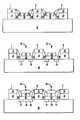
- FIG. 1illustrates a wafer having a plurality of gate structures on the wafer
- FIG. 2illustrates a step in accordance with a preferred embodiment of the present invention wherein a first spacer is deposited and etched, and then a silicon epitaxial layer is grown;
- FIG. 3illustrates a step in accordance with a preferred embodiment of the present invention wherein a second spacer is deposited and etched, and then a second silicon epitaxial layer is grown;
- FIG. 4illustrates a step in accordance with a preferred embodiment of the present invention wherein the second spacer is removed from around the gate structure and four junctions are formed by ion implantation;
- FIG. 5illustrates a step in accordance with a preferred embodiment of the present invention wherein a third spacer is deposited and etched, and then fifth and sixth junctions are formed by ion implantation.
- FIGS. 1 to 5illustrate a preferred embodiment of a process for fabricating transistor structures.
- FIG. 5also illustrates the transistor structure resulting from the fabrication process of FIGS. 1 to 5 .
- the processgenerally involves the formation and use of two silicon epitaxial layers on the transistor structure.
- the process illustrated in FIGS. 1 to 5is described with reference to the fabrication of DRAMs, however, the process can be used to fabricate other devices as well.
- FIG. 1the results of several preliminary steps in the fabrication of a DRAM are illustrated, whereby gate structures 7 , 8 and 9 , each including structures 10 and 15 , are formed on a wafer 16 .
- the structures 10are conductors and the structures 15 are insulators. These preliminary steps can be performed in accordance with well-known techniques of transistor fabrication.
- a SIN spaceris deposited on the surface of the wafer 16 as well as on top of and around the gate structures 7 , 8 and 9 . Then the SIN spacer is etched to remove it from the surface of the wafer 16 . As is illustrated in FIG. 2, after the deposition and etching of the spacer, a spacer structure 28 remains around the gate structures 7 , 8 and 9 . The spacer structure 28 will provide blocking of epi layer growth at the gate edge.
- the deposition and etching of spacersis well known, and can be accomplished in a variety of ways, with a variety of materials.
- the spacer structure 28preferably is a nitride spacer, but any oxide spacer process can be utilized.
- a silicon epitaxial layer 30is grown on the surface of the wafer 16 , as illustrated in FIG. 2 .
- the thickness of the silicon epitaxial layer 30is preferably in the range of 200 to 300 Angstroms, although the layer 30 may have a thickness outside this range. The thickness will depend on many different parameters, including but not limited to, the design parameters of the transistor being fabricated and the parameters of various steps of the fabrication process being used.
- the silicon epitaxial layer 30can be fabricated using well-known techniques.
- spacer structure 32will provide blocking of epi layer growth.
- the spacer structure 32preferably is fabricated using oxide deposition, and any oxides can be utilized.
- a second silicon epitaxial layer 34is grown on the surface of the first silicon epitaxial layer 30 , as illustrated in FIG. 3 .
- the second silicon epitaxial layer 34is not grown as close to the gate structures 7 , 8 and 9 as the first silicon epitaxial layer 30 due to the second spacer 32 .
- this structure of the epitaxial layers 30 and 34will allow the fabrication of junctions so that different areas of the junctions will have different characteristics.
- the thickness of the second silicon epitaxial layer 34is preferably thicker than the thickness of the first silicon epitaxial layer 30 , but need not be so. Thus, the thickness of the second silicon epitaxial layer 34 can be the same as, or less than, the thickness of the first silicon epitaxial layer 30 . In accordance with a preferred embodiment of the present invention, the thickness of the second silicon epitaxial layer 34 is in the range of 300 to 400 Angstroms. As with the first silicon epitaxial layer 30 , the second silicon epitaxial layer 34 may have a thickness outside this range. Also, as with the first silicon epitaxial layer 30 , the thickness of the second silicon epitaxial layer 34 will depend on many different parameters, including but not limited to, the design parameters of the transistor being fabricated and the parameters of various steps of the fabrication process being used.
- the second spacer 32is removed using oxide removal. Once the second spacer 32 is removed, the structure remaining is illustrated in FIG. 4 . As shown in FIG. 4, the junctions 24 , 25 , 26 and 27 are formed through ion implantation. The step of ion implantation is illustrated as arrows 36 . The junctions 24 , 25 , 26 and 27 can be formed using plasma conversion implantation, also referred to as plasma doping. These junctions 24 , 25 , 26 and 27 are formed near the gate structures 7 , 8 and 9 , as illustrated.
- the energy associated with the step of ion implantationis preferably low, such as is typically used to from a shallow junction. In accordance with one aspect of the present invention, the implantation energy is in the range of 5 keV to 10 keV. The implantation energy can also be in the range of 1 keV to 10 keV. Other implantation energy levels can be used during this step.
- Another spaceris deposited on the second silicon epitaxial layer 34 and around the gate structures 7 , 8 and 9 . This spacer is then etched to remove it from the second silicon epitaxial layer 34 . As is illustrated in FIG. 5, after the deposition and etching of the spacer, there is another spacer structure 46 that remains around the gate structures 7 , 8 and 9 .
- the spacer structure 46will provide blocking of deep implantation below the spacer structure 46 .
- the deposition and etching of spacersis well known, and can be accomplished in a variety of ways, with a variety of materials.
- the spacer structure 46preferably is fabricated using BPSG oxide deposition, but any insulators can be utilized.
- junctions 28 and 29are further formed by a second step of ion implantation.
- the second step of ion implantationis illustrated by arrows 48 .
- the junction 28is formed between the junctions 24 and 25 .
- the junction 29is formed between the junctions 26 and 27 .
- the energy associated with the second step of ion implantationis preferably higher than the energy associated with the first step of ion implantation.
- the energy level used in the second step of ion implementationcan be the same as is typically used to from a deep junction.
- the implantation energy used in the second step of ion implantationis 30 keV. In another embodiment, the implantation energy is 20 keV. Other implantation energy levels can also be used during this step.
- each of the junction areas 24 to 29have the same depth. This allows improved short channel effect.
- the depth of the junction areasmay, however, be different due to process factors.
Landscapes
- Insulated Gate Type Field-Effect Transistor (AREA)
Abstract
Description
Claims (16)
Priority Applications (2)
| Application Number | Priority Date | Filing Date | Title |
|---|---|---|---|
| US10/142,537US6537885B1 (en) | 2002-05-09 | 2002-05-09 | Transistor and method of manufacturing a transistor having a shallow junction formation using a two step EPI layer |
| DE10320598ADE10320598B4 (en) | 2002-05-09 | 2003-05-08 | A method of fabricating a flat implant transistor using a two-stage epitaxial layer process |
Applications Claiming Priority (1)
| Application Number | Priority Date | Filing Date | Title |
|---|---|---|---|
| US10/142,537US6537885B1 (en) | 2002-05-09 | 2002-05-09 | Transistor and method of manufacturing a transistor having a shallow junction formation using a two step EPI layer |
Publications (1)
| Publication Number | Publication Date |
|---|---|
| US6537885B1true US6537885B1 (en) | 2003-03-25 |
Family
ID=22500225
Family Applications (1)
| Application Number | Title | Priority Date | Filing Date |
|---|---|---|---|
| US10/142,537Expired - LifetimeUS6537885B1 (en) | 2002-05-09 | 2002-05-09 | Transistor and method of manufacturing a transistor having a shallow junction formation using a two step EPI layer |
Country Status (2)
| Country | Link |
|---|---|
| US (1) | US6537885B1 (en) |
| DE (1) | DE10320598B4 (en) |
Cited By (30)
| Publication number | Priority date | Publication date | Assignee | Title |
|---|---|---|---|---|
| US20040198060A1 (en)* | 2003-04-07 | 2004-10-07 | Ai-Sen Liu | Selective spacer layer deposition method for forming spacers with different widths |
| US20050142823A1 (en)* | 2003-12-31 | 2005-06-30 | Dongbuanam Semiconductor Inc. | Method of fabricating gate electrode of semiconductor device |
| US20050266692A1 (en)* | 2004-06-01 | 2005-12-01 | Brask Justin K | Method of patterning a film |
| US20060068591A1 (en)* | 2004-09-29 | 2006-03-30 | Marko Radosavljevic | Fabrication of channel wraparound gate structure for field-effect transistor |
| US20060086977A1 (en)* | 2004-10-25 | 2006-04-27 | Uday Shah | Nonplanar device with thinned lower body portion and method of fabrication |
| US20060128131A1 (en)* | 2004-09-29 | 2006-06-15 | Chang Peter L | Independently accessed double-gate and tri-gate transistors in same process flow |
| US20060202266A1 (en)* | 2005-03-14 | 2006-09-14 | Marko Radosavljevic | Field effect transistor with metal source/drain regions |
| US20060261411A1 (en)* | 2003-06-27 | 2006-11-23 | Hareland Scott A | Nonplanar device with stress incorporation layer and method of fabrication |
| US20070001173A1 (en)* | 2005-06-21 | 2007-01-04 | Brask Justin K | Semiconductor device structures and methods of forming semiconductor structures |
| US20070090408A1 (en)* | 2005-09-29 | 2007-04-26 | Amlan Majumdar | Narrow-body multiple-gate FET with dominant body transistor for high performance |
| US20070111419A1 (en)* | 2005-09-28 | 2007-05-17 | Doyle Brian S | CMOS Devices with a single work function gate electrode and method of fabrication |
| US20070152266A1 (en)* | 2005-12-29 | 2007-07-05 | Intel Corporation | Method and structure for reducing the external resistance of a three-dimensional transistor through use of epitaxial layers |
| US20070257324A1 (en)* | 2003-02-17 | 2007-11-08 | Deok-Hyung Lee | Semiconductor Devices Having Gate Structures and Contact Pads that are Lower than the Gate Structures |
| US20070262389A1 (en)* | 2004-01-16 | 2007-11-15 | Robert Chau | Tri-gate transistors and methods to fabricate same |
| US20080090397A1 (en)* | 2004-09-30 | 2008-04-17 | Brask Justin K | Nonplanar transistors with metal gate electrodes |
| US20080142841A1 (en)* | 2004-03-31 | 2008-06-19 | Nick Lindert | Bulk non-planar transistor having strained enhanced mobility and methods of fabrication |
| US20080157225A1 (en)* | 2006-12-29 | 2008-07-03 | Suman Datta | SRAM and logic transistors with variable height multi-gate transistor architecture |
| US20080188041A1 (en)* | 2005-08-17 | 2008-08-07 | Suman Datta | Lateral undercut of metal gate in SOI device |
| US20080258207A1 (en)* | 2005-06-30 | 2008-10-23 | Marko Radosavljevic | Block Contact Architectures for Nanoscale Channel Transistors |
| US7456476B2 (en) | 2003-06-27 | 2008-11-25 | Intel Corporation | Nonplanar semiconductor device with partially or fully wrapped around gate electrode and methods of fabrication |
| US7479421B2 (en) | 2005-09-28 | 2009-01-20 | Intel Corporation | Process for integrating planar and non-planar CMOS transistors on a bulk substrate and article made thereby |
| US7518196B2 (en) | 2005-02-23 | 2009-04-14 | Intel Corporation | Field effect transistor with narrow bandgap source and drain regions and method of fabrication |
| US20090250772A1 (en)* | 2008-04-08 | 2009-10-08 | Botula Alan B | Field effect transistor and method of manufacture |
| US20100200925A1 (en)* | 2001-09-20 | 2010-08-12 | Elpida Memory, Inc. | Semiconductor device and method of manufacturing the same |
| US20110062520A1 (en)* | 2005-06-15 | 2011-03-17 | Brask Justin K | Method for fabricating transistor with thinned channel |
| US7960794B2 (en) | 2004-08-10 | 2011-06-14 | Intel Corporation | Non-planar pMOS structure with a strained channel region and an integrated strained CMOS flow |
| US7989280B2 (en) | 2005-11-30 | 2011-08-02 | Intel Corporation | Dielectric interface for group III-V semiconductor device |
| US8084818B2 (en) | 2004-06-30 | 2011-12-27 | Intel Corporation | High mobility tri-gate devices and methods of fabrication |
| US8362566B2 (en) | 2008-06-23 | 2013-01-29 | Intel Corporation | Stress in trigate devices using complimentary gate fill materials |
| US8617945B2 (en) | 2006-08-02 | 2013-12-31 | Intel Corporation | Stacking fault and twin blocking barrier for integrating III-V on Si |
Citations (11)
| Publication number | Priority date | Publication date | Assignee | Title |
|---|---|---|---|---|
| US5079180A (en)* | 1988-12-22 | 1992-01-07 | Texas Instruments Incorporated | Method of fabricating a raised source/drain transistor |
| US5319232A (en)* | 1991-11-25 | 1994-06-07 | Motorola, Inc. | Transistor having a lightly doped region |
| US6063677A (en)* | 1996-10-28 | 2000-05-16 | Texas Instruments Incorporated | Method of forming a MOSFET using a disposable gate and raised source and drain |
| US6087235A (en)* | 1999-10-14 | 2000-07-11 | Advanced Micro Devices, Inc. | Method for effective fabrication of a field effect transistor with elevated drain and source contact structures |
| US6180978B1 (en)* | 1997-12-30 | 2001-01-30 | Texas Instruments Incorporated | Disposable gate/replacement gate MOSFETs for sub-0.1 micron gate length and ultra-shallow junctions |
| US6254676B1 (en)* | 1999-06-11 | 2001-07-03 | United Microelectronics Corp. | Method for manufacturing metal oxide semiconductor transistor having raised source/drain |
| US6326664B1 (en)* | 1994-12-23 | 2001-12-04 | Intel Corporation | Transistor with ultra shallow tip and method of fabrication |
| US6335214B1 (en)* | 2000-09-20 | 2002-01-01 | International Business Machines Corporation | SOI circuit with dual-gate transistors |
| US6346447B1 (en)* | 1997-08-29 | 2002-02-12 | Texas Instruments Incorporated | Shallow-implant elevated source/drain doping from a sidewall dopant source |
| US6355533B2 (en)* | 1999-12-24 | 2002-03-12 | Hyundai Electronics Industries Co., Ltd. | Method for manufacturing semiconductor device |
| US6445042B1 (en)* | 1999-06-15 | 2002-09-03 | Advanced Micro Devices, Inc. | Method and apparatus for making MOSFETs with elevated source/drain extensions |
- 2002
- 2002-05-09USUS10/142,537patent/US6537885B1/ennot_activeExpired - Lifetime
- 2003
- 2003-05-08DEDE10320598Apatent/DE10320598B4/ennot_activeExpired - Fee Related
Patent Citations (11)
| Publication number | Priority date | Publication date | Assignee | Title |
|---|---|---|---|---|
| US5079180A (en)* | 1988-12-22 | 1992-01-07 | Texas Instruments Incorporated | Method of fabricating a raised source/drain transistor |
| US5319232A (en)* | 1991-11-25 | 1994-06-07 | Motorola, Inc. | Transistor having a lightly doped region |
| US6326664B1 (en)* | 1994-12-23 | 2001-12-04 | Intel Corporation | Transistor with ultra shallow tip and method of fabrication |
| US6063677A (en)* | 1996-10-28 | 2000-05-16 | Texas Instruments Incorporated | Method of forming a MOSFET using a disposable gate and raised source and drain |
| US6346447B1 (en)* | 1997-08-29 | 2002-02-12 | Texas Instruments Incorporated | Shallow-implant elevated source/drain doping from a sidewall dopant source |
| US6180978B1 (en)* | 1997-12-30 | 2001-01-30 | Texas Instruments Incorporated | Disposable gate/replacement gate MOSFETs for sub-0.1 micron gate length and ultra-shallow junctions |
| US6254676B1 (en)* | 1999-06-11 | 2001-07-03 | United Microelectronics Corp. | Method for manufacturing metal oxide semiconductor transistor having raised source/drain |
| US6445042B1 (en)* | 1999-06-15 | 2002-09-03 | Advanced Micro Devices, Inc. | Method and apparatus for making MOSFETs with elevated source/drain extensions |
| US6087235A (en)* | 1999-10-14 | 2000-07-11 | Advanced Micro Devices, Inc. | Method for effective fabrication of a field effect transistor with elevated drain and source contact structures |
| US6355533B2 (en)* | 1999-12-24 | 2002-03-12 | Hyundai Electronics Industries Co., Ltd. | Method for manufacturing semiconductor device |
| US6335214B1 (en)* | 2000-09-20 | 2002-01-01 | International Business Machines Corporation | SOI circuit with dual-gate transistors |
Cited By (90)
| Publication number | Priority date | Publication date | Assignee | Title |
|---|---|---|---|---|
| US20100200925A1 (en)* | 2001-09-20 | 2010-08-12 | Elpida Memory, Inc. | Semiconductor device and method of manufacturing the same |
| US7511340B2 (en)* | 2003-02-17 | 2009-03-31 | Samsung Electronics Co., Ltd. | Semiconductor devices having gate structures and contact pads that are lower than the gate structures |
| US20070257324A1 (en)* | 2003-02-17 | 2007-11-08 | Deok-Hyung Lee | Semiconductor Devices Having Gate Structures and Contact Pads that are Lower than the Gate Structures |
| US20040198060A1 (en)* | 2003-04-07 | 2004-10-07 | Ai-Sen Liu | Selective spacer layer deposition method for forming spacers with different widths |
| US6943077B2 (en)* | 2003-04-07 | 2005-09-13 | Taiwan Semiconductor Manufacturing Co., Ltd. | Selective spacer layer deposition method for forming spacers with different widths |
| US20060113616A1 (en)* | 2003-04-07 | 2006-06-01 | Ai-Sen Liu | Selective spacer layer deposition method for forming spacers with different widths |
| US7714397B2 (en) | 2003-06-27 | 2010-05-11 | Intel Corporation | Tri-gate transistor device with stress incorporation layer and method of fabrication |
| US8405164B2 (en) | 2003-06-27 | 2013-03-26 | Intel Corporation | Tri-gate transistor device with stress incorporation layer and method of fabrication |
| US7820513B2 (en) | 2003-06-27 | 2010-10-26 | Intel Corporation | Nonplanar semiconductor device with partially or fully wrapped around gate electrode and methods of fabrication |
| US20060261411A1 (en)* | 2003-06-27 | 2006-11-23 | Hareland Scott A | Nonplanar device with stress incorporation layer and method of fabrication |
| US7456476B2 (en) | 2003-06-27 | 2008-11-25 | Intel Corporation | Nonplanar semiconductor device with partially or fully wrapped around gate electrode and methods of fabrication |
| US8273626B2 (en) | 2003-06-27 | 2012-09-25 | Intel Corporationn | Nonplanar semiconductor device with partially or fully wrapped around gate electrode and methods of fabrication |
| US7211491B2 (en) | 2003-12-31 | 2007-05-01 | Dongbu Electronics Co., Ltd. | Method of fabricating gate electrode of semiconductor device |
| US20050142823A1 (en)* | 2003-12-31 | 2005-06-30 | Dongbuanam Semiconductor Inc. | Method of fabricating gate electrode of semiconductor device |
| US20070262389A1 (en)* | 2004-01-16 | 2007-11-15 | Robert Chau | Tri-gate transistors and methods to fabricate same |
| US7781771B2 (en) | 2004-03-31 | 2010-08-24 | Intel Corporation | Bulk non-planar transistor having strained enhanced mobility and methods of fabrication |
| US20080142841A1 (en)* | 2004-03-31 | 2008-06-19 | Nick Lindert | Bulk non-planar transistor having strained enhanced mobility and methods of fabrication |
| US20050266692A1 (en)* | 2004-06-01 | 2005-12-01 | Brask Justin K | Method of patterning a film |
| US7579280B2 (en) | 2004-06-01 | 2009-08-25 | Intel Corporation | Method of patterning a film |
| US8084818B2 (en) | 2004-06-30 | 2011-12-27 | Intel Corporation | High mobility tri-gate devices and methods of fabrication |
| US7960794B2 (en) | 2004-08-10 | 2011-06-14 | Intel Corporation | Non-planar pMOS structure with a strained channel region and an integrated strained CMOS flow |
| US20060128131A1 (en)* | 2004-09-29 | 2006-06-15 | Chang Peter L | Independently accessed double-gate and tri-gate transistors in same process flow |
| US8268709B2 (en) | 2004-09-29 | 2012-09-18 | Intel Corporation | Independently accessed double-gate and tri-gate transistors in same process flow |
| US7915167B2 (en) | 2004-09-29 | 2011-03-29 | Intel Corporation | Fabrication of channel wraparound gate structure for field-effect transistor |
| US20110156145A1 (en)* | 2004-09-29 | 2011-06-30 | Marko Radosavljevic | Fabrication of channel wraparound gate structure for field-effect transistor |
| US20100297838A1 (en)* | 2004-09-29 | 2010-11-25 | Chang Peter L D | Independently accessed double-gate and tri-gate transistors in same process flow |
| US8399922B2 (en) | 2004-09-29 | 2013-03-19 | Intel Corporation | Independently accessed double-gate and tri-gate transistors |
| US7859053B2 (en) | 2004-09-29 | 2010-12-28 | Intel Corporation | Independently accessed double-gate and tri-gate transistors in same process flow |
| US20060068591A1 (en)* | 2004-09-29 | 2006-03-30 | Marko Radosavljevic | Fabrication of channel wraparound gate structure for field-effect transistor |
| US20080090397A1 (en)* | 2004-09-30 | 2008-04-17 | Brask Justin K | Nonplanar transistors with metal gate electrodes |
| US7528025B2 (en) | 2004-09-30 | 2009-05-05 | Intel Corporation | Nonplanar transistors with metal gate electrodes |
| US9741809B2 (en) | 2004-10-25 | 2017-08-22 | Intel Corporation | Nonplanar device with thinned lower body portion and method of fabrication |
| US7550333B2 (en) | 2004-10-25 | 2009-06-23 | Intel Corporation | Nonplanar device with thinned lower body portion and method of fabrication |
| US8502351B2 (en) | 2004-10-25 | 2013-08-06 | Intel Corporation | Nonplanar device with thinned lower body portion and method of fabrication |
| US20110062512A1 (en)* | 2004-10-25 | 2011-03-17 | Uday Shah | Nonplanar device with thinned lower body portion and method of fabrication |
| US8749026B2 (en) | 2004-10-25 | 2014-06-10 | Intel Corporation | Nonplanar device with thinned lower body portion and method of fabrication |
| US8067818B2 (en) | 2004-10-25 | 2011-11-29 | Intel Corporation | Nonplanar device with thinned lower body portion and method of fabrication |
| US9190518B2 (en) | 2004-10-25 | 2015-11-17 | Intel Corporation | Nonplanar device with thinned lower body portion and method of fabrication |
| US10236356B2 (en) | 2004-10-25 | 2019-03-19 | Intel Corporation | Nonplanar device with thinned lower body portion and method of fabrication |
| US20060086977A1 (en)* | 2004-10-25 | 2006-04-27 | Uday Shah | Nonplanar device with thinned lower body portion and method of fabrication |
| US7518196B2 (en) | 2005-02-23 | 2009-04-14 | Intel Corporation | Field effect transistor with narrow bandgap source and drain regions and method of fabrication |
| US20100295129A1 (en)* | 2005-02-23 | 2010-11-25 | Chau Robert S | Field effect transistor with narrow bandgap source and drain regions and method of fabrication |
| US7825481B2 (en) | 2005-02-23 | 2010-11-02 | Intel Corporation | Field effect transistor with narrow bandgap source and drain regions and method of fabrication |
| US8368135B2 (en) | 2005-02-23 | 2013-02-05 | Intel Corporation | Field effect transistor with narrow bandgap source and drain regions and method of fabrication |
| US7893506B2 (en) | 2005-02-23 | 2011-02-22 | Intel Corporation | Field effect transistor with narrow bandgap source and drain regions and method of fabrication |
| US8183646B2 (en) | 2005-02-23 | 2012-05-22 | Intel Corporation | Field effect transistor with narrow bandgap source and drain regions and method of fabrication |
| US20090142897A1 (en)* | 2005-02-23 | 2009-06-04 | Chau Robert S | Field effect transistor with narrow bandgap source and drain regions and method of fabrication |
| US8664694B2 (en) | 2005-02-23 | 2014-03-04 | Intel Corporation | Field effect transistor with narrow bandgap source and drain regions and method of fabrication |
| US8816394B2 (en) | 2005-02-23 | 2014-08-26 | Intel Corporation | Field effect transistor with narrow bandgap source and drain regions and method of fabrication |
| US9048314B2 (en) | 2005-02-23 | 2015-06-02 | Intel Corporation | Field effect transistor with narrow bandgap source and drain regions and method of fabrication |
| US20110121393A1 (en)* | 2005-02-23 | 2011-05-26 | Chau Robert S | Field effect transistor with narrow bandgap source and drain regions and method of fabrication |
| US9368583B2 (en) | 2005-02-23 | 2016-06-14 | Intel Corporation | Field effect transistor with narrow bandgap source and drain regions and method of fabrication |
| US7879675B2 (en) | 2005-03-14 | 2011-02-01 | Intel Corporation | Field effect transistor with metal source/drain regions |
| US20090325350A1 (en)* | 2005-03-14 | 2009-12-31 | Marko Radosavljevic | Field effect transistor with metal source/drain regions |
| US20060202266A1 (en)* | 2005-03-14 | 2006-09-14 | Marko Radosavljevic | Field effect transistor with metal source/drain regions |
| US11978799B2 (en) | 2005-06-15 | 2024-05-07 | Tahoe Research, Ltd. | Method for fabricating transistor with thinned channel |
| US20110062520A1 (en)* | 2005-06-15 | 2011-03-17 | Brask Justin K | Method for fabricating transistor with thinned channel |
| US9337307B2 (en) | 2005-06-15 | 2016-05-10 | Intel Corporation | Method for fabricating transistor with thinned channel |
| US9806195B2 (en) | 2005-06-15 | 2017-10-31 | Intel Corporation | Method for fabricating transistor with thinned channel |
| US20070001173A1 (en)* | 2005-06-21 | 2007-01-04 | Brask Justin K | Semiconductor device structures and methods of forming semiconductor structures |
| US9761724B2 (en) | 2005-06-21 | 2017-09-12 | Intel Corporation | Semiconductor device structures and methods of forming semiconductor structures |
| US8071983B2 (en) | 2005-06-21 | 2011-12-06 | Intel Corporation | Semiconductor device structures and methods of forming semiconductor structures |
| US8933458B2 (en) | 2005-06-21 | 2015-01-13 | Intel Corporation | Semiconductor device structures and methods of forming semiconductor structures |
| US9385180B2 (en) | 2005-06-21 | 2016-07-05 | Intel Corporation | Semiconductor device structures and methods of forming semiconductor structures |
| US20090218603A1 (en)* | 2005-06-21 | 2009-09-03 | Brask Justin K | Semiconductor device structures and methods of forming semiconductor structures |
| US7547637B2 (en) | 2005-06-21 | 2009-06-16 | Intel Corporation | Methods for patterning a semiconductor film |
| US8581258B2 (en) | 2005-06-21 | 2013-11-12 | Intel Corporation | Semiconductor device structures and methods of forming semiconductor structures |
| US7898041B2 (en) | 2005-06-30 | 2011-03-01 | Intel Corporation | Block contact architectures for nanoscale channel transistors |
| US20080258207A1 (en)* | 2005-06-30 | 2008-10-23 | Marko Radosavljevic | Block Contact Architectures for Nanoscale Channel Transistors |
| US20080188041A1 (en)* | 2005-08-17 | 2008-08-07 | Suman Datta | Lateral undercut of metal gate in SOI device |
| US7736956B2 (en) | 2005-08-17 | 2010-06-15 | Intel Corporation | Lateral undercut of metal gate in SOI device |
| US7479421B2 (en) | 2005-09-28 | 2009-01-20 | Intel Corporation | Process for integrating planar and non-planar CMOS transistors on a bulk substrate and article made thereby |
| US20070111419A1 (en)* | 2005-09-28 | 2007-05-17 | Doyle Brian S | CMOS Devices with a single work function gate electrode and method of fabrication |
| US7902014B2 (en) | 2005-09-28 | 2011-03-08 | Intel Corporation | CMOS devices with a single work function gate electrode and method of fabrication |
| US20110180851A1 (en)* | 2005-09-28 | 2011-07-28 | Doyle Brian S | Cmos devices with a single work function gate electrode and method of fabrication |
| US8294180B2 (en) | 2005-09-28 | 2012-10-23 | Intel Corporation | CMOS devices with a single work function gate electrode and method of fabrication |
| US8193567B2 (en) | 2005-09-28 | 2012-06-05 | Intel Corporation | Process for integrating planar and non-planar CMOS transistors on a bulk substrate and article made thereby |
| US20070090408A1 (en)* | 2005-09-29 | 2007-04-26 | Amlan Majumdar | Narrow-body multiple-gate FET with dominant body transistor for high performance |
| US7989280B2 (en) | 2005-11-30 | 2011-08-02 | Intel Corporation | Dielectric interface for group III-V semiconductor device |
| US20070152266A1 (en)* | 2005-12-29 | 2007-07-05 | Intel Corporation | Method and structure for reducing the external resistance of a three-dimensional transistor through use of epitaxial layers |
| US8617945B2 (en) | 2006-08-02 | 2013-12-31 | Intel Corporation | Stacking fault and twin blocking barrier for integrating III-V on Si |
| US20080157225A1 (en)* | 2006-12-29 | 2008-07-03 | Suman Datta | SRAM and logic transistors with variable height multi-gate transistor architecture |
| US8921190B2 (en)* | 2008-04-08 | 2014-12-30 | International Business Machines Corporation | Field effect transistor and method of manufacture |
| US20090250772A1 (en)* | 2008-04-08 | 2009-10-08 | Botula Alan B | Field effect transistor and method of manufacture |
| US9847415B2 (en) | 2008-04-08 | 2017-12-19 | Globalfoundries Inc. | Field effect transistor and method of manufacture |
| US9224754B2 (en) | 2008-06-23 | 2015-12-29 | Intel Corporation | Stress in trigate devices using complimentary gate fill materials |
| US9450092B2 (en) | 2008-06-23 | 2016-09-20 | Intel Corporation | Stress in trigate devices using complimentary gate fill materials |
| US8741733B2 (en) | 2008-06-23 | 2014-06-03 | Intel Corporation | Stress in trigate devices using complimentary gate fill materials |
| US9806193B2 (en) | 2008-06-23 | 2017-10-31 | Intel Corporation | Stress in trigate devices using complimentary gate fill materials |
| US8362566B2 (en) | 2008-06-23 | 2013-01-29 | Intel Corporation | Stress in trigate devices using complimentary gate fill materials |
Also Published As
| Publication number | Publication date |
|---|---|
| DE10320598B4 (en) | 2007-02-01 |
| DE10320598A1 (en) | 2004-01-08 |
Similar Documents
| Publication | Publication Date | Title |
|---|---|---|
| US6537885B1 (en) | Transistor and method of manufacturing a transistor having a shallow junction formation using a two step EPI layer | |
| JP4597531B2 (en) | Semiconductor device with retrograde dopant distribution in channel region and method for manufacturing such semiconductor device | |
| US7348243B2 (en) | Semiconductor device and method for fabricating the same | |
| KR100597460B1 (en) | Transistor and manufacturing method of semiconductor device | |
| US6359310B1 (en) | Shallow doped junctions with a variable profile gradation of dopants | |
| US6551881B1 (en) | Self-aligned dual-oxide umosfet device and a method of fabricating same | |
| JP4741187B2 (en) | High voltage power MOSFET including doped column | |
| CN102468334B (en) | VDMOS (Vertical Double-diffusion Metal Oxide Semiconductor Structure) device and manufacturing method thereof | |
| US20030183856A1 (en) | Semiconductor device having a retrograde dopant profile in a channel region and method for fabricating the same | |
| JP2000349093A (en) | Manufacturing process of MOS gate device with reduced number of masks | |
| US7524726B2 (en) | Method for fabricating a semiconductor device | |
| JP2005510088A (en) | Trench metal oxide semiconductor field effect transistor device with polycrystalline silicon source contact structure | |
| US20100200897A1 (en) | Transistor and method of manufacturing the same | |
| US8202782B2 (en) | Method of manufacturing transistor | |
| CN101689507A (en) | An extended drain transistor and a method of manufacturing the same | |
| US6593175B2 (en) | Method of controlling a shape of an oxide layer formed on a substrate | |
| CN110718452B (en) | Silicon carbide device and method for manufacturing same | |
| US6254676B1 (en) | Method for manufacturing metal oxide semiconductor transistor having raised source/drain | |
| CN115662902A (en) | Manufacturing method of trench type field effect transistor | |
| US6566680B1 (en) | Semiconductor-on-insulator (SOI) tunneling junction transistor | |
| US20050048707A1 (en) | Processing method for improving structure of a high voltage device | |
| JP2004063479A (en) | Semiconductor device and method of manufacturing the same | |
| US6878997B2 (en) | Compensation component and method for fabricating the component | |
| KR101164981B1 (en) | Method for fabricating semiconductor device | |
| CN104681437A (en) | Semiconductor device with strained channel and preparation method thereof |
Legal Events
| Date | Code | Title | Description |
|---|---|---|---|
| AS | Assignment | Owner name:INFINEON TECHNOLOGIES NORTH AMERICA CORP., CALIFOR Free format text:ASSIGNMENT OF ASSIGNORS INTEREST;ASSIGNORS:KANG, WOO-TAG;LEE, KIL-HO;REEL/FRAME:012902/0712 Effective date:20020503 | |
| FEPP | Fee payment procedure | Free format text:PAYOR NUMBER ASSIGNED (ORIGINAL EVENT CODE: ASPN); ENTITY STATUS OF PATENT OWNER: LARGE ENTITY | |
| STCF | Information on status: patent grant | Free format text:PATENTED CASE | |
| FPAY | Fee payment | Year of fee payment:4 | |
| AS | Assignment | Owner name:QIMONDA AG, GERMANY Free format text:ASSIGNMENT OF ASSIGNORS INTEREST;ASSIGNOR:INFINEON TECHNOLOGIES NORTH AMERICA CORP;REEL/FRAME:023774/0399 Effective date:20060425 | |
| FPAY | Fee payment | Year of fee payment:8 | |
| FPAY | Fee payment | Year of fee payment:12 | |
| AS | Assignment | Owner name:INFINEON TECHNOLOGIES AG, GERMANY Free format text:ASSIGNMENT OF ASSIGNORS INTEREST;ASSIGNOR:QIMONDA AG;REEL/FRAME:035623/0001 Effective date:20141009 | |
| AS | Assignment | Owner name:POLARIS INNOVATIONS LIMITED, IRELAND Free format text:ASSIGNMENT OF ASSIGNORS INTEREST;ASSIGNOR:INFINEON TECHNOLOGIES AG;REEL/FRAME:036818/0583 Effective date:20150708 |