US6535419B2 - Mixed mode multi-level indicator - Google Patents
Mixed mode multi-level indicatorDownload PDFInfo
- Publication number
- US6535419B2 US6535419B2US09/905,421US90542101AUS6535419B2US 6535419 B2US6535419 B2US 6535419B2US 90542101 AUS90542101 AUS 90542101AUS 6535419 B2US6535419 B2US 6535419B2
- Authority
- US
- United States
- Prior art keywords
- mode
- bit
- cells
- indicator
- memory device
- Prior art date
- Legal status (The legal status is an assumption and is not a legal conclusion. Google has not performed a legal analysis and makes no representation as to the accuracy of the status listed.)
- Expired - Lifetime
Links
- 238000000034methodMethods0.000claimsdescription11
- 238000010586diagramMethods0.000description4
- 238000009826distributionMethods0.000description4
- 238000003491arrayMethods0.000description1
- 230000005669field effectEffects0.000description1
- 230000005055memory storageEffects0.000description1
- 238000012986modificationMethods0.000description1
- 230000004048modificationEffects0.000description1
Images


Classifications
- G—PHYSICS
- G11—INFORMATION STORAGE
- G11C—STATIC STORES
- G11C11/00—Digital stores characterised by the use of particular electric or magnetic storage elements; Storage elements therefor
- G11C11/56—Digital stores characterised by the use of particular electric or magnetic storage elements; Storage elements therefor using storage elements with more than two stable states represented by steps, e.g. of voltage, current, phase, frequency
- G11C11/5621—Digital stores characterised by the use of particular electric or magnetic storage elements; Storage elements therefor using storage elements with more than two stable states represented by steps, e.g. of voltage, current, phase, frequency using charge storage in a floating gate
- G—PHYSICS
- G11—INFORMATION STORAGE
- G11C—STATIC STORES
- G11C2211/00—Indexing scheme relating to digital stores characterized by the use of particular electric or magnetic storage elements; Storage elements therefor
- G11C2211/56—Indexing scheme relating to G11C11/56 and sub-groups for features not covered by these groups
- G11C2211/564—Miscellaneous aspects
- G11C2211/5641—Multilevel memory having cells with different number of storage levels
Definitions
- a flash memory cellcan be a field effect transistor (FET) that includes a select gate, a floating gate, a drain, and a source.
- FETfield effect transistor
- a cellcan be read by grounding the source, and applying a voltage to a bitline connected with the drain. By applying a voltage to the wordline connected to the select gate, the cell can be switched on and off.
- Programming a cellincludes trapping excess electrons in the floating gate to increase voltage. This reduces the current conducted by the memory cell when the select voltage is applied to the select gate.
- the cellis programmed when the cell current is less than a reference current when the select voltage is applied.
- the cellis erased when the cell current is greater than the reference current and the select voltage is applied.
- a multi-level cellis a cell that can be programmed with more than one voltage level. Each voltage level is mapped to corresponding bits of information. For example, a single multi-level cell can be programmed with one of four voltage levels, e.g. ⁇ 2.5V, 0.0V, +1.0V, +2.0V that correspond to binary bits “00”, “01”, “10”, and “11”, respectively.
- a cell that is programmable at more voltage levelscan store more bits of data based on Eqn. 1.
- Bis the number of bits of data stored
- Nis the number of voltage levels.
- a 1 bit cellrequires 2 voltage levels
- a 2 bit cellrequires 4 voltage levels
- a 3 bit cellrequires 8 voltage levels
- a 4 bit cellrequires 16 voltage levels.
- FIG. 1shows a representation of a single bit programming voltage level diagram 100 .
- the “erase state” program distribution 102 (“erase state”), and the “programmed state” program distribution 104 (“programmed state”)represent a single bit being either a “0” or a “1”, respectively.
- the voltage between the upper end 106 of the erase state 102 and ground 108 (0.0V)is the “erase margin.”
- the erase state program distribution 102is center near ⁇ 2.5V and the programmed state program distribution 104 is centered around 2.25V.
- the read pointcan be at ground 108 or anywhere between lines 106 and 110 , preferably near the mid-point between lines 106 and 110 .
- FIG. 2shows a representation of a four level multilevel cell program voltage diagram 200 .
- the program distribution (“distribution”) of the four levelsare shown at 210 , 212 , 214 , and 216 respectively.
- the programming distributionsare located at approximately ⁇ 2.5V, 0.0V, 0.8V, and 2.0V and the width of the programming distributions are approximately 100 to 600 mV.
- a four level multilevel memory cellcan be programmed with any one of these voltage levels. Because the cell can store one of four binary values it can store 2 bits of information.
- the program marginalso called “margin”, “data margin”, or “guard band” is the voltage levels between distributions that is not normally used.
- the program margins between program distributions 212 , 214 , and 216are approximately 800 mV to 100 mV wide.
- the program margin between program distributions 210 and 212is approximately 2.0V.
- a memory devicehaving a plurality of memory cells that are group into at least two group of cells. Each cell is capable of being programmed in at least two modes.
- a mode indicatoris associated with each group of cells. The mode indicator indicates which programming mode is used to access the cells.
- the mode indicatoris one or more bits and optionally is user selectable.
- FIG. 1is a representation of a single bit programming voltage level
- FIG. 2is a representation of a two bit programming voltage level
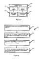
- FIG. 3is a representation of an embodiment of a memory device with mode indicators
- FIG. 4is a flow diagram of a method of access two segments of memory in two different access modes.
- a user selectable mode indicatoris associated with each page of memory.
- the mode indicatorindicates which mode of the page (or group). That is, the multi-level mode or the single bit mode. If more than two modes are used, the mode indicator will be more than one bit.
- a two bit mode indicatorindicates four modes and a three bit indicator indicates eight modes. Preferably, the modes are “single bit” and “two bit” and only a single bit is required for the mode indicator for each page.
- the mode indicatoris a single bit
- the default statepreferably indicates the single bit state.
- Multi-level cells while holding more information than a single bit cellcan take substantially longer to program, have smaller program margins, and have lower reliability. Further, NAND based Multi-level cells are usually addressed on a page-by-page basis.
- a 64 Mbit (8 Mbyte) memory arraycan contain 4096 pages where each page contains 512 bytes.
- a pagecan be a 4K bit page that has 4096 bits.
- Interlaced NAND based multi-level cellsare read sequentially. For example, if the byte at location 10 is to be read, the bytes at locations 0 through 9 must be read first. That is, interlaced NAND based multi-level cells do not support partial page writes or reads.
- the first read accesscan be performed at the same voltage level, e.g. 206 (FIG. 2 ).
- the mode indicatorWhen the mode indicator is in the erase state (e.g. zero), indicating the single bit mode, the reference level will be lowered to 108 (FIG. 1) without significant impact on access times.
- the mode indicatorWhen the mode indicator is in the programmed state, indicating the multi-bit mode, the memory is accessed with normal MLC access times.
- the initial read accessis similar for both modes. After the initial access, if the mode indicator is set to the multi-level mode a second access would occur.
- FIG. 3is an embodiment of a memory device 300 with two groups of memory cells 302 , 304 and two mode indicators 306 , 308 associated with the respective groups of memory cells.
- the groups of memory cells 302 , 304can be physically separate memory or, preferably, they are subsets of one physical memory.
- the mode indicators 306 , 308can be locations in memory, including the being part of the same memory as the first and second groups of memory 302 , 304 .
- the mode indicators 306 , 308can be a register, non-volatile memory, or volatile memory.
- the memory device 300can include a storage means for storing data capable of storing data in a plurality of storage formats, an indication means for indicating which of the plurality of different formats is to be used to access the data, and an input/output means for accessing the data stored in the storage means.
- the storage meanscan include memory cells, memory arrays, flash memory, NAND flash memory, or any other memory storage device.
- the plurality of storage formatscan preferably include a single-bit and a multi-bit format. Multiple multi-bit formats can also be used.
- the indicator meanscan include a single memory cell, multiple memory cells, a latch, or other device for storing a value.
- the storage meanscan include a plurality of storage areas and the indicator means can include a separate indicator for each storage area.
- the indicator means with separate indicators for each storage areacan be a group of memory cells, a group of latches, or other device for storing the indicators.
- a storage areacan be a page of memory including a 4096 bit page of memory.
- the storage areascan be of varying sizes and need not each be of equal size.
- FIG. 4is a flow diagram of an embodiment of a method 400 of accessing multi-bit memory cells.
- the methodincludes determining a first mode value from a first mode indicator 402 then accessing the first segment of multi-bit cells using an access mode corresponding to the first mode value 404 .
- the first mode indicatorbeing associated with a first segment of multi-bit memory cells.
- the first mode indicatorbeing capable of indicating at least a first and second mode.
- the first modeincluding single bit access and the second mode including multi-bit access.
- the method 400includes determining a second mode value from a second mode indicator, then accessing the second segment of multi-bit cells using an access mode corresponding to the second mode value.
- the second mode indicatorbeing associated with a second segment of multi-bit memory cells and being capable of indicating at least a first and second mode.
- the first modeincluding single bit access and the second mode including multi-bit access.
Landscapes
- Engineering & Computer Science (AREA)
- Computer Hardware Design (AREA)
- Read Only Memory (AREA)
Abstract
Description
Claims (20)
Priority Applications (1)
| Application Number | Priority Date | Filing Date | Title |
|---|---|---|---|
| US09/905,421US6535419B2 (en) | 2000-02-25 | 2001-07-13 | Mixed mode multi-level indicator |
Applications Claiming Priority (2)
| Application Number | Priority Date | Filing Date | Title |
|---|---|---|---|
| US09/513,402US6297988B1 (en) | 2000-02-25 | 2000-02-25 | Mode indicator for multi-level memory |
| US09/905,421US6535419B2 (en) | 2000-02-25 | 2001-07-13 | Mixed mode multi-level indicator |
Related Parent Applications (1)
| Application Number | Title | Priority Date | Filing Date |
|---|---|---|---|
| US09/513,402ContinuationUS6297988B1 (en) | 2000-02-25 | 2000-02-25 | Mode indicator for multi-level memory |
Publications (2)
| Publication Number | Publication Date |
|---|---|
| US20010038553A1 US20010038553A1 (en) | 2001-11-08 |
| US6535419B2true US6535419B2 (en) | 2003-03-18 |
Family
ID=24043112
Family Applications (2)
| Application Number | Title | Priority Date | Filing Date |
|---|---|---|---|
| US09/513,402Expired - LifetimeUS6297988B1 (en) | 2000-02-25 | 2000-02-25 | Mode indicator for multi-level memory |
| US09/905,421Expired - LifetimeUS6535419B2 (en) | 2000-02-25 | 2001-07-13 | Mixed mode multi-level indicator |
Family Applications Before (1)
| Application Number | Title | Priority Date | Filing Date |
|---|---|---|---|
| US09/513,402Expired - LifetimeUS6297988B1 (en) | 2000-02-25 | 2000-02-25 | Mode indicator for multi-level memory |
Country Status (2)
| Country | Link |
|---|---|
| US (2) | US6297988B1 (en) |
| WO (1) | WO2001063614A1 (en) |
Cited By (11)
| Publication number | Priority date | Publication date | Assignee | Title |
|---|---|---|---|---|
| US20060004952A1 (en)* | 2004-02-15 | 2006-01-05 | M-Systems Flash Disk Pioneers, Ltd. | Method of managing a multi-bit-cell flash memory |
| US20070002613A1 (en)* | 2005-06-30 | 2007-01-04 | Intel Corporation | Memory array with pseudo single bit memory cell and method |
| US20070064480A1 (en)* | 2005-09-20 | 2007-03-22 | Tiao-Hua Kuo | Multi-bit flash memory device having improved program rate |
| US20070133249A1 (en)* | 2005-12-09 | 2007-06-14 | Micron Technology, Inc. | Single level cell programming in a multiple level cell non-volatile memory device |
| US20080049516A1 (en)* | 2005-08-29 | 2008-02-28 | Spansion L.L.C. | Flash memory device having improved program rate |
| US7352626B1 (en) | 2005-08-29 | 2008-04-01 | Spansion Llc | Voltage regulator with less overshoot and faster settling time |
| US20080172521A1 (en)* | 2007-01-16 | 2008-07-17 | Samsung Electronics Co., Ltd. | Memory System Determining Storage Mode According to Host Provided Data Information |
| US20080316824A1 (en)* | 2007-06-22 | 2008-12-25 | Samsung Electronics Co., Ltd. | Non-volatile memory device and method of operating the same |
| US20090080247A1 (en)* | 2007-09-25 | 2009-03-26 | Sandisk Il Ltd | Using mlc flash as slc by writing dummy data |
| US7957204B1 (en) | 2005-09-20 | 2011-06-07 | Spansion Llc | Flash memory programming power reduction |
| US8358543B1 (en) | 2005-09-20 | 2013-01-22 | Spansion Llc | Flash memory programming with data dependent control of source lines |
Families Citing this family (31)
| Publication number | Priority date | Publication date | Assignee | Title |
|---|---|---|---|---|
| TW477949B (en)* | 1999-12-20 | 2002-03-01 | Winbond Electronics Corp | Data processing system |
| US6297988B1 (en)* | 2000-02-25 | 2001-10-02 | Advanced Micro Devices, Inc. | Mode indicator for multi-level memory |
| KR100386296B1 (en)* | 2000-12-30 | 2003-06-02 | 주식회사 하이닉스반도체 | Circuit for programming and reading flash memory with multiple levels and method for the same |
| US6717847B2 (en)* | 2001-09-17 | 2004-04-06 | Sandisk Corporation | Selective operation of a multi-state non-volatile memory system in a binary mode |
| US7554842B2 (en)* | 2001-09-17 | 2009-06-30 | Sandisk Corporation | Multi-purpose non-volatile memory card |
| EP1298670B1 (en)* | 2001-09-28 | 2007-03-07 | STMicroelectronics S.r.l. | Method for storing and reading data in a multilevel nonvolatile memory with a non-binary number of levels, and architecture therefor |
| US7260677B1 (en)* | 2003-07-16 | 2007-08-21 | Unisys Corporation | Programmable system and method for accessing a shared memory |
| US8019928B2 (en)* | 2004-02-15 | 2011-09-13 | Sandisk Il Ltd. | Method of managing a multi-bit-cell flash memory |
| US8082382B2 (en)* | 2004-06-04 | 2011-12-20 | Micron Technology, Inc. | Memory device with user configurable density/performance |
| US7535759B2 (en)* | 2004-06-04 | 2009-05-19 | Micron Technology, Inc. | Memory system with user configurable density/performance option |
| US7493457B2 (en)* | 2004-11-08 | 2009-02-17 | Sandisk Il. Ltd | States encoding in multi-bit flash cells for optimizing error rate |
| KR100732628B1 (en)* | 2005-07-28 | 2007-06-27 | 삼성전자주식회사 | Flash memory device for storing multi-bit data and single-bit data |
| CN101273413B (en) | 2005-09-29 | 2011-11-16 | 特科2000国际有限公司 | Portable Data Storage Using Single-Level Cell and Multi-Level Cell Flash Memory |
| US20070083697A1 (en)* | 2005-10-07 | 2007-04-12 | Microsoft Corporation | Flash memory management |
| US8848442B2 (en)* | 2006-03-06 | 2014-09-30 | Sandisk Il Ltd. | Multi-bit-per-cell flash memory device with non-bijective mapping |
| US7388781B2 (en)* | 2006-03-06 | 2008-06-17 | Sandisk Il Ltd. | Multi-bit-per-cell flash memory device with non-bijective mapping |
| US7911834B2 (en)* | 2006-05-15 | 2011-03-22 | Apple Inc. | Analog interface for a flash memory die |
| US7568135B2 (en) | 2006-05-15 | 2009-07-28 | Apple Inc. | Use of alternative value in cell detection |
| US7701797B2 (en)* | 2006-05-15 | 2010-04-20 | Apple Inc. | Two levels of voltage regulation supplied for logic and data programming voltage of a memory device |
| US7639542B2 (en)* | 2006-05-15 | 2009-12-29 | Apple Inc. | Maintenance operations for multi-level data storage cells |
| US8000134B2 (en) | 2006-05-15 | 2011-08-16 | Apple Inc. | Off-die charge pump that supplies multiple flash devices |
| KR100833188B1 (en) | 2006-11-03 | 2008-05-28 | 삼성전자주식회사 | Nonvolatile memory system that stores data in single-level cells or multi-level cells, depending on the nature of the data |
| US7460398B1 (en)* | 2007-06-19 | 2008-12-02 | Micron Technology, Inc. | Programming a memory with varying bits per cell |
| US7916536B2 (en) | 2007-07-26 | 2011-03-29 | Micron Technology, Inc. | Programming based on controller performance requirements |
| US8407400B2 (en)* | 2008-11-12 | 2013-03-26 | Micron Technology, Inc. | Dynamic SLC/MLC blocks allocations for non-volatile memory |
| WO2010077408A1 (en) | 2008-12-31 | 2010-07-08 | Rambus Inc. | Pattern-sensitive coding of data for storage in multi-level memory cells |
| KR101005120B1 (en)* | 2009-02-04 | 2011-01-04 | 주식회사 하이닉스반도체 | Program Method of Nonvolatile Memory Device |
| US9058881B1 (en)* | 2013-12-05 | 2015-06-16 | Sandisk Technologies Inc. | Systems and methods for partial page programming of multi level cells |
| US11194516B2 (en) | 2019-10-08 | 2021-12-07 | Micron Technology, Inc. | Media type selection |
| US11397526B2 (en) | 2020-02-28 | 2022-07-26 | Micron Technology, Inc. | Media type selection for image data |
| US11537321B2 (en) | 2020-07-14 | 2022-12-27 | Micron Technology, Inc. | Data selection based on quality |
Citations (8)
| Publication number | Priority date | Publication date | Assignee | Title |
|---|---|---|---|---|
| US5574879A (en) | 1994-06-02 | 1996-11-12 | Intel Corporation | Addressing modes for a dynamic single bit per cell to multiple bit per cell memory |
| EP0763828A2 (en) | 1995-09-13 | 1997-03-19 | Kabushiki Kaisha Toshiba | Nonvolatile semiconductor memory device and method for using the same |
| US5844841A (en)* | 1996-04-19 | 1998-12-01 | Kabushiki Kaisha Toshiba | Memory system |
| US5859795A (en)* | 1996-01-31 | 1999-01-12 | Sgs-Thomson Microelectronics S.R.L. | Multi-level memory circuits and corresponding reading and writing methods |
| US5930167A (en)* | 1997-07-30 | 1999-07-27 | Sandisk Corporation | Multi-state non-volatile flash memory capable of being its own two state write cache |
| DE19904542A1 (en) | 1998-07-17 | 2000-01-20 | Mitsubishi Electric Corp | Multi-bit dynamic random-access memory e.g. for personal computer is switched between binary memory mode and multi-value memory mode in response to mode selection signal fed to mode register |
| US6297988B1 (en)* | 2000-02-25 | 2001-10-02 | Advanced Micro Devices, Inc. | Mode indicator for multi-level memory |
| US6353553B1 (en)* | 2000-01-24 | 2002-03-05 | Mitsubishi Denki Kabushiki Kaisha | Nonvolatile semiconductor memory device having structure storing multivalued data and data storage system comprising the nonvolatile semiconductor memory device |
Family Cites Families (18)
| Publication number | Priority date | Publication date | Assignee | Title |
|---|---|---|---|---|
| US4567579A (en)* | 1983-07-08 | 1986-01-28 | Texas Instruments Incorporated | Dynamic memory with high speed nibble mode |
| US5602789A (en) | 1991-03-12 | 1997-02-11 | Kabushiki Kaisha Toshiba | Electrically erasable and programmable non-volatile and multi-level memory systemn with write-verify controller |
| JP3109537B2 (en) | 1991-07-12 | 2000-11-20 | 日本電気株式会社 | Read-only semiconductor memory device |
| US5175450A (en) | 1991-08-23 | 1992-12-29 | Micron Technology, Inc. | Apparatus for providing multi-level potentials at a sense node |
| US5689679A (en) | 1993-04-28 | 1997-11-18 | Digital Equipment Corporation | Memory system and method for selective multi-level caching using a cache level code |
| JP3179943B2 (en) | 1993-07-12 | 2001-06-25 | 株式会社東芝 | Semiconductor storage device |
| US5523972A (en) | 1994-06-02 | 1996-06-04 | Intel Corporation | Method and apparatus for verifying the programming of multi-level flash EEPROM memory |
| JP3469362B2 (en) | 1994-08-31 | 2003-11-25 | 株式会社東芝 | Semiconductor storage device |
| US5563828A (en)* | 1994-12-27 | 1996-10-08 | Intel Corporation | Method and apparatus for searching for data in multi-bit flash EEPROM memory arrays |
| US5541886A (en)* | 1994-12-27 | 1996-07-30 | Intel Corporation | Method and apparatus for storing control information in multi-bit non-volatile memory arrays |
| US5596526A (en) | 1995-08-15 | 1997-01-21 | Lexar Microsystems, Inc. | Non-volatile memory system of multi-level transistor cells and methods using same |
| JP3392604B2 (en) | 1995-11-14 | 2003-03-31 | 株式会社東芝 | Nonvolatile semiconductor memory device |
| US5862074A (en)* | 1996-10-04 | 1999-01-19 | Samsung Electronics Co., Ltd. | Integrated circuit memory devices having reconfigurable nonvolatile multi-bit memory cells therein and methods of operating same |
| JP3397600B2 (en) | 1996-11-01 | 2003-04-14 | 株式会社東芝 | Nonvolatile semiconductor memory device |
| JP3409986B2 (en) | 1997-01-31 | 2003-05-26 | 株式会社東芝 | Multi-valued memory |
| JP3517081B2 (en) | 1997-05-22 | 2004-04-05 | 株式会社東芝 | Multi-level nonvolatile semiconductor memory device |
| JPH1125681A (en) | 1997-06-27 | 1999-01-29 | Nec Corp | Non-volatile semiconductor storage device |
| US6768165B1 (en) | 1997-08-01 | 2004-07-27 | Saifun Semiconductors Ltd. | Two bit non-volatile electrically erasable and programmable semiconductor memory cell utilizing asymmetrical charge trapping |
- 2000
- 2000-02-25USUS09/513,402patent/US6297988B1/ennot_activeExpired - Lifetime
- 2001
- 2001-02-06WOPCT/US2001/003858patent/WO2001063614A1/enactiveApplication Filing
- 2001-07-13USUS09/905,421patent/US6535419B2/ennot_activeExpired - Lifetime
Patent Citations (9)
| Publication number | Priority date | Publication date | Assignee | Title |
|---|---|---|---|---|
| US5574879A (en) | 1994-06-02 | 1996-11-12 | Intel Corporation | Addressing modes for a dynamic single bit per cell to multiple bit per cell memory |
| EP0763828A2 (en) | 1995-09-13 | 1997-03-19 | Kabushiki Kaisha Toshiba | Nonvolatile semiconductor memory device and method for using the same |
| US5859795A (en)* | 1996-01-31 | 1999-01-12 | Sgs-Thomson Microelectronics S.R.L. | Multi-level memory circuits and corresponding reading and writing methods |
| US5844841A (en)* | 1996-04-19 | 1998-12-01 | Kabushiki Kaisha Toshiba | Memory system |
| US5930167A (en)* | 1997-07-30 | 1999-07-27 | Sandisk Corporation | Multi-state non-volatile flash memory capable of being its own two state write cache |
| DE19904542A1 (en) | 1998-07-17 | 2000-01-20 | Mitsubishi Electric Corp | Multi-bit dynamic random-access memory e.g. for personal computer is switched between binary memory mode and multi-value memory mode in response to mode selection signal fed to mode register |
| US6104641A (en)* | 1998-07-17 | 2000-08-15 | Mitsubishi Denki Kabushiki Kaisha | Switchable multi bit semiconductor memory device |
| US6353553B1 (en)* | 2000-01-24 | 2002-03-05 | Mitsubishi Denki Kabushiki Kaisha | Nonvolatile semiconductor memory device having structure storing multivalued data and data storage system comprising the nonvolatile semiconductor memory device |
| US6297988B1 (en)* | 2000-02-25 | 2001-10-02 | Advanced Micro Devices, Inc. | Mode indicator for multi-level memory |
Cited By (25)
| Publication number | Priority date | Publication date | Assignee | Title |
|---|---|---|---|---|
| US20060004952A1 (en)* | 2004-02-15 | 2006-01-05 | M-Systems Flash Disk Pioneers, Ltd. | Method of managing a multi-bit-cell flash memory |
| US7716413B2 (en) | 2004-02-15 | 2010-05-11 | Sandisk Il Ltd. | Method of making a multi-bit-cell flash memory |
| US8024509B2 (en) | 2004-04-23 | 2011-09-20 | Sandisk Il Ltd. | Method of managing a multi-bit-cell flash memory |
| US20080123412A1 (en)* | 2004-04-23 | 2008-05-29 | Sandisk Il Ltd. | Method of managing a multi-bit-cell flash memory |
| US20070002613A1 (en)* | 2005-06-30 | 2007-01-04 | Intel Corporation | Memory array with pseudo single bit memory cell and method |
| US7272041B2 (en)* | 2005-06-30 | 2007-09-18 | Intel Corporation | Memory array with pseudo single bit memory cell and method |
| US20070268758A1 (en)* | 2005-06-30 | 2007-11-22 | Intel Corporation | Memory Array with Psedudo Single Bit Memory Cell and Method |
| US7525840B2 (en) | 2005-06-30 | 2009-04-28 | Intel Corporation | Memory array with pseudo single bit memory cell and method |
| US20080049516A1 (en)* | 2005-08-29 | 2008-02-28 | Spansion L.L.C. | Flash memory device having improved program rate |
| US7352626B1 (en) | 2005-08-29 | 2008-04-01 | Spansion Llc | Voltage regulator with less overshoot and faster settling time |
| US7453724B2 (en) | 2005-08-29 | 2008-11-18 | Spansion, Llc | Flash memory device having improved program rate |
| US7433228B2 (en)* | 2005-09-20 | 2008-10-07 | Spansion Llc | Multi-bit flash memory device having improved program rate |
| US8358543B1 (en) | 2005-09-20 | 2013-01-22 | Spansion Llc | Flash memory programming with data dependent control of source lines |
| US8462564B1 (en) | 2005-09-20 | 2013-06-11 | Spansion Llc | Flash memory programming power reduction |
| US7957204B1 (en) | 2005-09-20 | 2011-06-07 | Spansion Llc | Flash memory programming power reduction |
| US20070064480A1 (en)* | 2005-09-20 | 2007-03-22 | Tiao-Hua Kuo | Multi-bit flash memory device having improved program rate |
| US20080144373A1 (en)* | 2005-12-09 | 2008-06-19 | Micron Technology, Inc. | Single level cell programming in a multiple level cell non-volatile memory device |
| US7366013B2 (en)* | 2005-12-09 | 2008-04-29 | Micron Technology, Inc. | Single level cell programming in a multiple level cell non-volatile memory device |
| US7529129B2 (en) | 2005-12-09 | 2009-05-05 | Micron Technology, Inc. | Single level cell programming in a multiple level cell non-volatile memory device |
| US20070133249A1 (en)* | 2005-12-09 | 2007-06-14 | Micron Technology, Inc. | Single level cell programming in a multiple level cell non-volatile memory device |
| US20080172521A1 (en)* | 2007-01-16 | 2008-07-17 | Samsung Electronics Co., Ltd. | Memory System Determining Storage Mode According to Host Provided Data Information |
| US20080316824A1 (en)* | 2007-06-22 | 2008-12-25 | Samsung Electronics Co., Ltd. | Non-volatile memory device and method of operating the same |
| US8050087B2 (en)* | 2007-06-22 | 2011-11-01 | Samsung Electronics Co., Ltd. | Non-volatile memory device including block state confirmation cell and method of operating the same |
| US20090080247A1 (en)* | 2007-09-25 | 2009-03-26 | Sandisk Il Ltd | Using mlc flash as slc by writing dummy data |
| US7545673B2 (en)* | 2007-09-25 | 2009-06-09 | Sandisk Il Ltd. | Using MLC flash as SLC by writing dummy data |
Also Published As
| Publication number | Publication date |
|---|---|
| US20010038553A1 (en) | 2001-11-08 |
| US6297988B1 (en) | 2001-10-02 |
| WO2001063614A1 (en) | 2001-08-30 |
Similar Documents
| Publication | Publication Date | Title |
|---|---|---|
| US6535419B2 (en) | Mixed mode multi-level indicator | |
| US6343033B1 (en) | Variable pulse width memory programming | |
| US5815434A (en) | Multiple writes per a single erase for a nonvolatile memory | |
| US6219276B1 (en) | Multilevel cell programming | |
| US5574879A (en) | Addressing modes for a dynamic single bit per cell to multiple bit per cell memory | |
| US7274600B2 (en) | NAND flash memory with read and verification threshold uniformity | |
| US8082382B2 (en) | Memory device with user configurable density/performance | |
| US8862860B2 (en) | Flash storage partial page caching | |
| US6967896B2 (en) | Address scramble | |
| US20120039123A1 (en) | Multiple level programming in a non-volatile memory device | |
| US5936906A (en) | Multilevel sense device for a flash memory | |
| US6424569B1 (en) | User selectable cell programming | |
| KR960005355B1 (en) | Nonvolatile semiconductor storage and storage system using that | |
| US5999445A (en) | Multilevel non-volatile memory devices | |
| US6707713B1 (en) | Interlaced multi-level memory | |
| WO1996008825A1 (en) | Memory with multiple erase modes | |
| US6891758B2 (en) | Position based erase verification levels in a flash memory device | |
| JP2000011699A (en) | Semiconductor storage device | |
| HK1016737B (en) | Multiple writes per a single erase for a nonvolatile memory | |
| HK1015519A1 (en) | Multiple writes per a single erase for a nonvolatile memory |
Legal Events
| Date | Code | Title | Description |
|---|---|---|---|
| STCF | Information on status: patent grant | Free format text:PATENTED CASE | |
| FPAY | Fee payment | Year of fee payment:4 | |
| AS | Assignment | Owner name:SPANSION INC., CALIFORNIA Free format text:ASSIGNMENT OF ASSIGNORS INTEREST;ASSIGNOR:ADVANCED MICRO DEVICES, INC.;REEL/FRAME:019047/0532 Effective date:20070131 | |
| AS | Assignment | Owner name:SPANSION LLC, CALIFORNIA Free format text:ASSIGNMENT OF ASSIGNORS INTEREST;ASSIGNOR:SPANSION INC.;REEL/FRAME:019069/0301 Effective date:20070131 | |
| AS | Assignment | Owner name:BARCLAYS BANK PLC,NEW YORK Free format text:SECURITY AGREEMENT;ASSIGNORS:SPANSION LLC;SPANSION INC.;SPANSION TECHNOLOGY INC.;AND OTHERS;REEL/FRAME:024522/0338 Effective date:20100510 Owner name:BARCLAYS BANK PLC, NEW YORK Free format text:SECURITY AGREEMENT;ASSIGNORS:SPANSION LLC;SPANSION INC.;SPANSION TECHNOLOGY INC.;AND OTHERS;REEL/FRAME:024522/0338 Effective date:20100510 | |
| FPAY | Fee payment | Year of fee payment:8 | |
| FPAY | Fee payment | Year of fee payment:12 | |
| AS | Assignment | Owner name:SPANSION TECHNOLOGY INC., CALIFORNIA Free format text:TERMINATION AND RELEASE OF SECURITY INTEREST IN PATENT COLLATERAL;ASSIGNOR:BARCLAYS BANK PLC;REEL/FRAME:034715/0305 Effective date:20141227 Owner name:SPANSION TECHNOLOGY LLC, CALIFORNIA Free format text:TERMINATION AND RELEASE OF SECURITY INTEREST IN PATENT COLLATERAL;ASSIGNOR:BARCLAYS BANK PLC;REEL/FRAME:034715/0305 Effective date:20141227 Owner name:SPANSION INC., CALIFORNIA Free format text:TERMINATION AND RELEASE OF SECURITY INTEREST IN PATENT COLLATERAL;ASSIGNOR:BARCLAYS BANK PLC;REEL/FRAME:034715/0305 Effective date:20141227 Owner name:SPANSION LLC, CALIFORNIA Free format text:TERMINATION AND RELEASE OF SECURITY INTEREST IN PATENT COLLATERAL;ASSIGNOR:BARCLAYS BANK PLC;REEL/FRAME:034715/0305 Effective date:20141227 | |
| AS | Assignment | Owner name:CYPRESS SEMICONDUCTOR CORPORATION, CALIFORNIA Free format text:ASSIGNMENT OF ASSIGNORS INTEREST;ASSIGNOR:SPANSION, LLC;REEL/FRAME:036025/0453 Effective date:20150601 | |
| AS | Assignment | Owner name:SPANSION LLC, CALIFORNIA Free format text:PARTIAL RELEASE OF SECURITY INTEREST IN PATENTS;ASSIGNOR:MORGAN STANLEY SENIOR FUNDING, INC., AS COLLATERAL AGENT;REEL/FRAME:039708/0001 Effective date:20160811 Owner name:CYPRESS SEMICONDUCTOR CORPORATION, CALIFORNIA Free format text:PARTIAL RELEASE OF SECURITY INTEREST IN PATENTS;ASSIGNOR:MORGAN STANLEY SENIOR FUNDING, INC., AS COLLATERAL AGENT;REEL/FRAME:039708/0001 Effective date:20160811 | |
| AS | Assignment | Owner name:MONTEREY RESEARCH, LLC, CALIFORNIA Free format text:ASSIGNMENT OF ASSIGNORS INTEREST;ASSIGNOR:CYPRESS SEMICONDUCTOR CORPORATION;REEL/FRAME:040911/0238 Effective date:20160811 |