US6535403B1 - Systems and methods for inverter waveform smoothing - Google Patents
Systems and methods for inverter waveform smoothingDownload PDFInfo
- Publication number
- US6535403B1 US6535403B1US09/932,773US93277301AUS6535403B1US 6535403 B1US6535403 B1US 6535403B1US 93277301 AUS93277301 AUS 93277301AUS 6535403 B1US6535403 B1US 6535403B1
- Authority
- US
- United States
- Prior art keywords
- ripple
- current
- turn
- determining
- amplitude
- Prior art date
- Legal status (The legal status is an assumption and is not a legal conclusion. Google has not performed a legal analysis and makes no representation as to the accuracy of the status listed.)
- Expired - Lifetime
Links
- 238000009499grossingMethods0.000titleclaimsabstractdescription7
- 238000000034methodMethods0.000titleclaimsdescription20
- 238000012986modificationMethods0.000claimsabstractdescription15
- 230000004048modificationEffects0.000claimsabstractdescription15
- 239000004065semiconductorSubstances0.000claimsdescription12
- 238000011084recoveryMethods0.000claimsdescription6
- 230000002457bidirectional effectEffects0.000claims1
- 238000006073displacement reactionMethods0.000abstractdescription3
- 230000000694effectsEffects0.000description6
- 239000003990capacitorSubstances0.000description4
- 230000001934delayEffects0.000description4
- 238000010586diagramMethods0.000description4
- 230000006399behaviorEffects0.000description2
- 230000001419dependent effectEffects0.000description1
- 238000001514detection methodMethods0.000description1
- 230000001939inductive effectEffects0.000description1
- 238000005259measurementMethods0.000description1
Images


Classifications
- H—ELECTRICITY
- H02—GENERATION; CONVERSION OR DISTRIBUTION OF ELECTRIC POWER
- H02M—APPARATUS FOR CONVERSION BETWEEN AC AND AC, BETWEEN AC AND DC, OR BETWEEN DC AND DC, AND FOR USE WITH MAINS OR SIMILAR POWER SUPPLY SYSTEMS; CONVERSION OF DC OR AC INPUT POWER INTO SURGE OUTPUT POWER; CONTROL OR REGULATION THEREOF
- H02M1/00—Details of apparatus for conversion
- H02M1/12—Arrangements for reducing harmonics from AC input or output
- H—ELECTRICITY
- H02—GENERATION; CONVERSION OR DISTRIBUTION OF ELECTRIC POWER
- H02M—APPARATUS FOR CONVERSION BETWEEN AC AND AC, BETWEEN AC AND DC, OR BETWEEN DC AND DC, AND FOR USE WITH MAINS OR SIMILAR POWER SUPPLY SYSTEMS; CONVERSION OF DC OR AC INPUT POWER INTO SURGE OUTPUT POWER; CONTROL OR REGULATION THEREOF
- H02M7/00—Conversion of AC power input into DC power output; Conversion of DC power input into AC power output
- H02M7/42—Conversion of DC power input into AC power output without possibility of reversal
- H02M7/44—Conversion of DC power input into AC power output without possibility of reversal by static converters
- H02M7/48—Conversion of DC power input into AC power output without possibility of reversal by static converters using discharge tubes with control electrode or semiconductor devices with control electrode
- H02M7/53—Conversion of DC power input into AC power output without possibility of reversal by static converters using discharge tubes with control electrode or semiconductor devices with control electrode using devices of a triode or transistor type requiring continuous application of a control signal
- H02M7/537—Conversion of DC power input into AC power output without possibility of reversal by static converters using discharge tubes with control electrode or semiconductor devices with control electrode using devices of a triode or transistor type requiring continuous application of a control signal using semiconductor devices only, e.g. single switched pulse inverters
- H02M7/5387—Conversion of DC power input into AC power output without possibility of reversal by static converters using discharge tubes with control electrode or semiconductor devices with control electrode using devices of a triode or transistor type requiring continuous application of a control signal using semiconductor devices only, e.g. single switched pulse inverters in a bridge configuration
- H02M7/53871—Conversion of DC power input into AC power output without possibility of reversal by static converters using discharge tubes with control electrode or semiconductor devices with control electrode using devices of a triode or transistor type requiring continuous application of a control signal using semiconductor devices only, e.g. single switched pulse inverters in a bridge configuration with automatic control of output voltage or current
Definitions
- the present inventionrelates in general to switch-mode converters and, more particularly, to compensation of voltage loss at the output of switch-mode converters.
- Switch-mode converters employing pulse width modulationare widely used for dc-dc and dc-ac applications.
- a switch-mode converteris used in a dc-ac inverter configuration to produce a power-frequency sinusoidal waveform.
- Delays in device turn-onare present in this type of converter, and are typically of two types: (1) intentional (programmed) delays to avoid simultaneous conduction (shoot-through) of the upper and lower switching devices; and (2) delays associated with the turn-on characteristics of the switching devices and reverse recovery characteristics of the parallel diodes. These two types of delay combine to produce an effective voltage loss at the output of the converter. This voltage loss depends on switching conditions and can therefore show up in the output waveform as a notch, which causes a departure from purely sinusoidal conditions.
- the notch phenomenonhas been explored by others with a focus on operation of the converter at high (rated) power levels.
- the prior artcompensates for the notching at high power levels by adding a small compensating voltage with polarity determined from measurement of the load current polarity.
- the prior artdoes not address aspects of the notching behavior that are seen readily only at lower converter voltage or power levels. Because the analysis presented by the prior art is incomplete, the solutions described therein are also incomplete. Solutions based solely on load current polarity are inadequate for notch correction at low converter power levels.
- the present inventionis directed to systems and methods of compensating for notching in a way that restores a substantially pure sinusoidal output voltage waveform to the output of a converter, regardless of the load current level, power level, or power factor (both distortion and displacement power factor).
- a method of waveform smoothing for a waveform in a switch-mode converter having a DC bus voltage and an output filter inductancecomprises determining a ripple current in the converter; determining a time-to-zero; determining a turn-on time; determining the lesser of the time-to-zero and the turn-on time; determining a duty cycle modification based on the lesser of the time-to-zero and the turn-on time; and applying the duty cycle modification to the waveform.
- a switch-mode converter systemcomprises a first half-bridge connected to an LC circuit comprising an output filter inductor and an output filter capacitor and adapted to generate a pulse width modulation (PWM) output voltage having a distorted output voltage waveform; an input voltage source connected in parallel with the first half-bridge; a bus capacitor connected in parallel with the input voltage; and a controller adapted to determine a ripple current and compensate for the distorted output voltage waveform responsive to the ripple current.
- PWMpulse width modulation
- a second half-bridgeis connected in parallel with the first half-bridge, the input voltage source is connected in parallel with the first and second half-bridges, and the second half-bridge is connected to the LC circuit. According to other aspects of the invention, the second half-bridge is connected to another LC circuit.
- FIG. 1is a schematic circuit diagram of an exemplary inverter system that is helpful in explaining the present invention
- FIG. 2is a schematic circuit diagram of an exemplary half-bridge in accordance with the present invention.
- FIGS. 3A, 3 B, 3 C, and 3 Dshow various inductor current waveshapes for explaining various scenarios in accordance with the present invention
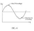
- FIG. 4shows an exemplary output voltage waveshape with notching
- FIG. 5is a flowchart of an exemplary method of waveform smoothing in accordance with the present invention.
- the present inventionrelates to the application of a switch-mode converter in a dc-ac inverter configuration that produces a power-frequency sinusoidal waveform. Notching is compensated for, such that a substantially pure sinusoidal output voltage waveform is provided, regardless of the load current level, power level, or power factor (both distortion and displacement power factor).
- FIG. 1is a schematic circuit diagram of an exemplary inverter that is helpful in explaining the present invention.
- the converter shownis a single-phase full-bridge inverter.
- Each of the two half-bridges shown in FIG. 1produces a high-frequency PWM output voltage that, when filtered by the LC circuits shown, results in a sinusoidal power frequency voltage at the output terminals.
- the converteris controlled in such a way that the power frequency voltages produced at the two terminals are phase shifted 180 degrees, resulting in a total output voltage with amplitude twice that of each half-bridge.
- the inverter of the system of FIG. 1comprises an input voltage source V 1 , a bus capacitor C 0 , two half-bridges (such as those shown in FIG. 2) comprising transistors Q 1 and Q 2 or comprising transistors Q 3 and Q 4, output filter inductors L 1 and L 2 , output filter capacitors C 1 and C 2 , an optional transformer T 1 , and a load.
- a controller 10controls the inverter in accordance with the present invention.
- the controller 10can be a micro-processor, for example, or any other programmable control device that can implement the methods described herein.
- a half-bridgecomprises two semiconductor switches in series that are either ON or OFF.
- the two semiconductor switches comprising a half-bridgeare preferably not turned on simultaneously because that would result in a short-circuit across the dc bus (this condition is also referred to as a shoot-through).
- the output of the bridgeis tied to the positive side of the dc bus.
- the output of the bridgeis tied to the negative side of the dc bus.
- Power semiconductor componentstypically contain an anti-parallel diode which allows current to flow in the reverse direction through the switch even when the switch is not being gated. Since the half-bridges carry inductive load current, the current coming out of the half-bridge will remain continuous. When a switch is turned OFF, the current that was flowing through that switch will instead flow through the anti-parallel diode of the other switch.
- a programmed delayis included between the turn-off of one device and the turn-on of the other device in each half-bridge.
- This delay(referred to as the deadband, dead time, or blanking time) along with other delays associated with device turn-on and diode reverse recovery characteristics, results in a small time interval during the PWM cycle in which neither the upper nor the lower switching device is carrying current.
- the currentis carried entirely by the anti-parallel diodes (or MOSFET body diodes), and the voltage during this short time depends on the direction of the inductor current.
- FIG. 2is a schematic circuit diagram of an exemplary half-bridge in accordance with the present invention.
- positive inductor current I Li.e., flowing into the load
- diode D 2diode D 2 (during the deadband) and therefore connects the output terminal to the zero volt dc bus, resulting in a small net loss of output voltage during that short time interval.
- Negative inductor current(away from the load) connects the output terminal to the high voltage dc bus through diode D 1 (during the deadband), resulting in a small net gain of output voltage during the short time interval.
- FIGS. 3A, 3 B, 3 C, and 3 Dshow various inductor current waveshapes, including ripple caused by PWM switching, for explaining various scenarios in accordance with the present invention.
- the load currentis high enough that the total current (load current plus ripple current) is always positive.
- the load currentis negative, and the total current is always negative.
- the magnitude of the load currentis less than the ripple current, resulting in both positive and negative intervals.
- the current in FIG. 3Ashould produce a net loss in output voltage
- the current in FIG. 3Bshould produce a net gain in output voltage.
- the current in FIGS. 3C and 3Dproduces a net loss in output voltage during the positive interval and a net gain in output voltage during the negative interval, resulting in virtually zero net effect over the complete PWM cycle.
- FIG. 4shows an exemplary output voltage waveshape with notching.
- the above-described behaviorsresult in distortion of the output voltage waveform as shown in FIG. 4 .
- a net voltage lossoccurs when the current is positive and its magnitude exceeds the ripple current magnitude.
- a net voltage gainoccurs (output voltage less negative than it would otherwise be) when the current is negative and its magnitude exceeds the ripple current magnitude.
- the voltage gainscancel the voltage losses during switching, resulting in zero net effect on the output waveform.
- correction of the output voltage distortiontherefore preferably includes determination of the inductor current in order to give accurate results for low load current.
- the compensating algorithms described by othersare overly simplistic in that they include only detection of load current polarity without consideration of the inductor ripple current. For this reason, these techniques cannot be accurate for low output power levels.
- the compensating techniques described by othersset forth a small fixed voltage compensation that is applied dependent solely on the current polarity.
- the present inventionincludes sufficient accuracy to compensate for the voltage distortion, with consideration of relevant factors.
- the inventorshave determined the following relationships that are implemented by the controller 10 to compensate for the voltage distortion.
- Equation (1)describes a relationship for determining the ripple current, where I ripple is the ripple current.
- I rippleD ⁇ ( 1 - D ) ⁇ V d 2 ⁇ Lf c ( 1 )
- Equation (2)describes a relationship for determining the ripple current, and includes the effect of load current change during PWM switching cycle:
- I rippleV d 8 ⁇ Lf c ⁇ [ 1 - 4 ⁇ L 2 V d 2 ⁇ ( V 1 L + ⁇ I load ⁇ t ) 2 ] ⁇ ⁇
- ⁇ ⁇ V 1V d 2 ⁇ ( 2 ⁇ D - 1 ) ( 2 )
- equation (1)For high PWM switching frequencies, the load current does not change significantly during the PWM switching cycle, and equation (1) may be used. For lower PWM switching frequencies, it is desirable to include the effect of load current change over the switching cycle, and equation (2) is preferably used.
- T zeroL DV d ⁇ ( ⁇ I load ⁇ - I ripple ) ( 3 )
- Equation (4)is used to determine the time-to-on-state, including programmed dead time, device turn on characteristic, and diode reverse recovery characteristic.
- T onT DT + ( ⁇ I load ⁇ - I ripple + I RR ) ⁇ I device / ⁇ t ( 4 )
- T DTis the programmable dead time delay
- I RRis the parallel diode reverse recovery current
- dI device /dtis the switching device turn-on di/dt.
- FIG. 5is a flowchart of an exemplary method of waveform smoothing (i.e., correction for voltage distortion due to notching) in accordance with the present invention.
- the ripple currentis determined at step 110 using either equation (1) or (2).
- the time-to-zerois determined using equation (3) at step 120 . (Note: for symmetry, it is desirable to use D during positive half-cycle of output voltage, and (1 ⁇ D) during negative half-cycle.)
- the turn-on timeis then determined at step 130 using equation (4).
- the minimum of time-to-zero (equation (3)) and turn-on time (equation (4))is then taken at step 140 . This operation gives a gradual correction of waveform distortion as load current begins to exceed ripple current.
- the time value from step 140is used to determine the duty cycle modification at step 150 (equation (5)).
- This techniquecan be used in any converter or inverter which is capable of supporting bi-directional current flow and uses dead-time delay in operating its semiconductor switches (such as would be done for an inverter/converter comprising a half-bridge).
- the present inventionhas been used with a residential power system (RPS) converter and correctly restores the output voltage waveform to a sinusoid regardless of the load current amplitude. It is contemplated that the present invention is implemented in DSP converter control software.
- RPSresidential power system
Landscapes
- Engineering & Computer Science (AREA)
- Power Engineering (AREA)
- Dc-Dc Converters (AREA)
Abstract
Description


Claims (25)


Priority Applications (1)
| Application Number | Priority Date | Filing Date | Title |
|---|---|---|---|
| US09/932,773US6535403B1 (en) | 2001-08-17 | 2001-08-17 | Systems and methods for inverter waveform smoothing |
Applications Claiming Priority (1)
| Application Number | Priority Date | Filing Date | Title |
|---|---|---|---|
| US09/932,773US6535403B1 (en) | 2001-08-17 | 2001-08-17 | Systems and methods for inverter waveform smoothing |
Publications (1)
| Publication Number | Publication Date |
|---|---|
| US6535403B1true US6535403B1 (en) | 2003-03-18 |
Family
ID=25462892
Family Applications (1)
| Application Number | Title | Priority Date | Filing Date |
|---|---|---|---|
| US09/932,773Expired - LifetimeUS6535403B1 (en) | 2001-08-17 | 2001-08-17 | Systems and methods for inverter waveform smoothing |
Country Status (1)
| Country | Link |
|---|---|
| US (1) | US6535403B1 (en) |
Cited By (9)
| Publication number | Priority date | Publication date | Assignee | Title |
|---|---|---|---|---|
| US20040071002A1 (en)* | 2002-10-09 | 2004-04-15 | Rosenbaum Rodger H. | Method and apparatus for reducing no-load core loss in inverters |
| US20050035724A1 (en)* | 2002-01-02 | 2005-02-17 | Peter Lurkens | Electronic circuit, and method of operating a high-pressure lamp |
| US20050077842A1 (en)* | 2002-01-02 | 2005-04-14 | Ulrich Boke | Circuit arrangement for operation of one or more lamps |
| US20050184716A1 (en)* | 2004-02-20 | 2005-08-25 | International Rectifier Corporation | Apparatus and method for minimizing power loss associated with dead time |
| WO2005124498A1 (en)* | 2004-06-21 | 2005-12-29 | Xantrex International | Output power factor control of pulse-width modulated inverter |
| WO2006025782A1 (en)* | 2004-08-31 | 2006-03-09 | Abb Technology Ltd | Voltage source converter |
| US20060092588A1 (en)* | 2004-10-28 | 2006-05-04 | Realmuto Richard A | Multiple bi-directional input/output power control system |
| WO2009049079A1 (en)* | 2007-10-11 | 2009-04-16 | Smartspark Energy Systems, Inc. | Methods for minimizing double-frequency ripple power in single-phase power conditioners |
| US20140334192A1 (en)* | 2011-12-07 | 2014-11-13 | Noliac A/S | Piezoelectric power converter with bi-directional power transfer |
Citations (5)
| Publication number | Priority date | Publication date | Assignee | Title |
|---|---|---|---|---|
| US3950691A (en) | 1973-09-28 | 1976-04-13 | Shunjiro Ohba | High-output solid state dc-ac inverter with improved overload protection and control logic circuitry |
| US4502106A (en)* | 1983-10-17 | 1985-02-26 | Sundstrand Corporation | Current source sine wave inverter |
| US5168437A (en) | 1990-11-13 | 1992-12-01 | Westinghouse Electric Corp. | Phase displaced, multiple inverter bridge circuits with waveform notching for harmonic elimination |
| US5625548A (en)* | 1994-08-10 | 1997-04-29 | American Superconductor Corporation | Control circuit for cryogenically-cooled power electronics employed in power conversion systems |
| US6154379A (en)* | 1998-07-16 | 2000-11-28 | Tdk Corporation | Electric power conversion device |
- 2001
- 2001-08-17USUS09/932,773patent/US6535403B1/ennot_activeExpired - Lifetime
Patent Citations (5)
| Publication number | Priority date | Publication date | Assignee | Title |
|---|---|---|---|---|
| US3950691A (en) | 1973-09-28 | 1976-04-13 | Shunjiro Ohba | High-output solid state dc-ac inverter with improved overload protection and control logic circuitry |
| US4502106A (en)* | 1983-10-17 | 1985-02-26 | Sundstrand Corporation | Current source sine wave inverter |
| US5168437A (en) | 1990-11-13 | 1992-12-01 | Westinghouse Electric Corp. | Phase displaced, multiple inverter bridge circuits with waveform notching for harmonic elimination |
| US5625548A (en)* | 1994-08-10 | 1997-04-29 | American Superconductor Corporation | Control circuit for cryogenically-cooled power electronics employed in power conversion systems |
| US6154379A (en)* | 1998-07-16 | 2000-11-28 | Tdk Corporation | Electric power conversion device |
Non-Patent Citations (2)
| Title |
|---|
| A. Lindberg, PWM and Control of Two and Three Level High Power Voltage Source Converters, Royal Institute of Technology, Dept. of Electrical Engineering, Stockholm, Sweden, 1995 (Ph. D. Thesis), p. 119. No month. |
| N. Mohan, T. Undeland, W. Robbins, Power Electronics-Converters, No month Applications, and Design, Wiley & Sons, New York, NY 1995, pp. 236-239. |
Cited By (20)
| Publication number | Priority date | Publication date | Assignee | Title |
|---|---|---|---|---|
| US20050035724A1 (en)* | 2002-01-02 | 2005-02-17 | Peter Lurkens | Electronic circuit, and method of operating a high-pressure lamp |
| US20050077842A1 (en)* | 2002-01-02 | 2005-04-14 | Ulrich Boke | Circuit arrangement for operation of one or more lamps |
| US7030568B2 (en)* | 2002-01-02 | 2006-04-18 | Koninklijke Philips Electronics N.V. | Circuit arrangement for operation of one or more lamps |
| US20040071002A1 (en)* | 2002-10-09 | 2004-04-15 | Rosenbaum Rodger H. | Method and apparatus for reducing no-load core loss in inverters |
| US20050184716A1 (en)* | 2004-02-20 | 2005-08-25 | International Rectifier Corporation | Apparatus and method for minimizing power loss associated with dead time |
| US7391194B2 (en) | 2004-02-20 | 2008-06-24 | International Rectifier Corporation | Apparatus and method for minimizing power loss associated with dead time |
| US7660139B2 (en) | 2004-06-21 | 2010-02-09 | Xantrex International | Output power factor control of pulse-width modulated inverter |
| WO2005124498A1 (en)* | 2004-06-21 | 2005-12-29 | Xantrex International | Output power factor control of pulse-width modulated inverter |
| US20070247876A1 (en)* | 2004-06-21 | 2007-10-25 | Djordje Garabandic | Output Power Factor Control of Pulse-Width Modulated Inverter |
| WO2006025782A1 (en)* | 2004-08-31 | 2006-03-09 | Abb Technology Ltd | Voltage source converter |
| US20060092588A1 (en)* | 2004-10-28 | 2006-05-04 | Realmuto Richard A | Multiple bi-directional input/output power control system |
| WO2009049079A1 (en)* | 2007-10-11 | 2009-04-16 | Smartspark Energy Systems, Inc. | Methods for minimizing double-frequency ripple power in single-phase power conditioners |
| US20090097283A1 (en)* | 2007-10-11 | 2009-04-16 | Krein Philip T | Methods for Minimizing Double-Frequency Ripple Power in Single-Phase Power Conditioners |
| US7755916B2 (en)* | 2007-10-11 | 2010-07-13 | Solarbridge Technologies, Inc. | Methods for minimizing double-frequency ripple power in single-phase power conditioners |
| US20100238690A1 (en)* | 2007-10-11 | 2010-09-23 | Krein Philip T | Methods for minimizing double-frquency ripple power in single-phase power conditioners |
| CN101939898A (en)* | 2007-10-11 | 2011-01-05 | 太阳架技术公司 | Method for minimizing double-frequency ripple power in single-phase power regulators |
| US8004865B2 (en) | 2007-10-11 | 2011-08-23 | Solarbridge Technologies, Inc. | Methods for minimizing double-frequency ripple power in single-phase power conditioners |
| CN101939898B (en)* | 2007-10-11 | 2015-05-20 | 太阳架技术公司 | Method for Minimizing Dual-Frequency Ripple Power in Single-Phase Power Regulators |
| US20140334192A1 (en)* | 2011-12-07 | 2014-11-13 | Noliac A/S | Piezoelectric power converter with bi-directional power transfer |
| US20140334193A1 (en)* | 2011-12-07 | 2014-11-13 | Noliac A/S | Self-oscillating loop based piezoelectric power converter |
Similar Documents
| Publication | Publication Date | Title |
|---|---|---|
| US8644035B2 (en) | Load adaptive variable frequency phase-shift full-bridge DC/DC converter | |
| US5038267A (en) | Soft-switching power converter for operation in discrete pulse modulation and pulse width modulation modes | |
| US10566909B2 (en) | DC-DC converter and method for operating same | |
| US7525293B1 (en) | Power supply switching circuit for a halogen lamp | |
| EP2722979A1 (en) | Switch mode converter including auxiliary commutation circuit for achieving zero current switching | |
| US20120069615A1 (en) | Bridgeless power factor correction converter | |
| JPH03128672A (en) | Resonant inverter with improved control | |
| EP3249795B1 (en) | Dc/dc converter | |
| US5771164A (en) | Power supply converter for suppressing higher harmonics to output a stable voltage | |
| US9343973B2 (en) | Power conversion apparatus | |
| JP2017199628A (en) | Single stage commercial frequency to high frequency converter for induction heating and control method thereof | |
| US11736031B2 (en) | Unfolder-based single-stage AC-AC conversion system | |
| US6535403B1 (en) | Systems and methods for inverter waveform smoothing | |
| US5862043A (en) | Switch coupled active forward converter for obtaining a high power factor at a single power stage | |
| JP2002238257A (en) | Control method of resonance type DC-DC converter | |
| US11316423B2 (en) | Half-bridge having power semiconductors | |
| US10177681B2 (en) | Power converter including an autotransformer and power conversion method | |
| JP2817670B2 (en) | Wide input piezoelectric transformer inverter | |
| JP2000262070A (en) | Power converter | |
| JP2000217363A (en) | Power supply | |
| CN113366753A (en) | DC pulse power supply device | |
| JPH01321868A (en) | Pwm electric power converting device and control thereof | |
| JP4338334B2 (en) | Driving method of switching power supply | |
| US7330359B2 (en) | Power supply unit | |
| JPH06237577A (en) | Capacitor charging power supply |
Legal Events
| Date | Code | Title | Description |
|---|---|---|---|
| AS | Assignment | Owner name:ABB INC., CONNECTICUT Free format text:ASSIGNMENT OF ASSIGNORS INTEREST;ASSIGNORS:JUNGREIS, AARON M.;DICKMANDER, DAVID L.;PARKER, JEFFERY;REEL/FRAME:012417/0552;SIGNING DATES FROM 20010810 TO 20010813 | |
| AS | Assignment | Owner name:ABB T&D TECHNOLOGY LTD., SWITZERLAND Free format text:INVALID DOCUMENT;ASSIGNOR:ABB INC.;REEL/FRAME:012753/0976 Effective date:20020313 Owner name:ABB T&D TECHNOLOGY LTD., SWITZERLAND Free format text:ASSIGNMENT OF ASSIGNORS INTEREST;ASSIGNOR:ABB INC.;REEL/FRAME:012897/0132 Effective date:20020313 | |
| AS | Assignment | Owner name:ABB TECHNOLOGY AG, SWITZERLAND Free format text:ASSIGNMENT OF ASSIGNORS INTEREST;ASSIGNOR:ABB T&D TECHNOLOGY LTD.;REEL/FRAME:013173/0672 Effective date:20020319 | |
| FEPP | Fee payment procedure | Free format text:PAYOR NUMBER ASSIGNED (ORIGINAL EVENT CODE: ASPN); ENTITY STATUS OF PATENT OWNER: LARGE ENTITY | |
| STCF | Information on status: patent grant | Free format text:PATENTED CASE | |
| REMI | Maintenance fee reminder mailed | ||
| FPAY | Fee payment | Year of fee payment:4 | |
| SULP | Surcharge for late payment | ||
| FPAY | Fee payment | Year of fee payment:8 | |
| FPAY | Fee payment | Year of fee payment:12 | |
| AS | Assignment | Owner name:ABB SCHWEIZ AG, SWITZERLAND Free format text:MERGER;ASSIGNOR:ABB TECHNOLOGY LTD;REEL/FRAME:040800/0327 Effective date:20160509 |