US6535020B1 - Output buffer with compensated slew rate and delay control - Google Patents
Output buffer with compensated slew rate and delay controlDownload PDFInfo
- Publication number
- US6535020B1 US6535020B1US10/024,884US2488401AUS6535020B1US 6535020 B1US6535020 B1US 6535020B1US 2488401 AUS2488401 AUS 2488401AUS 6535020 B1US6535020 B1US 6535020B1
- Authority
- US
- United States
- Prior art keywords
- transistor
- drive transistor
- gate
- circuit
- compensation
- Prior art date
- Legal status (The legal status is an assumption and is not a legal conclusion. Google has not performed a legal analysis and makes no representation as to the accuracy of the status listed.)
- Expired - Lifetime
Links
- 238000000034methodMethods0.000claimsabstractdescription94
- 230000008569processEffects0.000claimsabstractdescription93
- 230000001419dependent effectEffects0.000claimsabstractdescription14
- 230000007704transitionEffects0.000claimsdescription32
- 230000004044responseEffects0.000claimsdescription13
- 230000007423decreaseEffects0.000claimsdescription8
- 230000008859changeEffects0.000claimsdescription4
- 230000000295complement effectEffects0.000claims2
- 230000001934delayEffects0.000description7
- 238000010586diagramMethods0.000description7
- 238000007599dischargingMethods0.000description4
- 238000004519manufacturing processMethods0.000description4
- 239000004065semiconductorSubstances0.000description3
- 238000006243chemical reactionMethods0.000description2
- 230000004048modificationEffects0.000description2
- 238000012986modificationMethods0.000description2
- 238000001311chemical methods and processMethods0.000description1
- 230000003247decreasing effectEffects0.000description1
- 239000002019doping agentSubstances0.000description1
- 238000005516engineering processMethods0.000description1
- 239000007943implantSubstances0.000description1
- 230000009467reductionEffects0.000description1
- 230000000630rising effectEffects0.000description1
- 235000012431wafersNutrition0.000description1
Images


Classifications
- H—ELECTRICITY
- H03—ELECTRONIC CIRCUITRY
- H03K—PULSE TECHNIQUE
- H03K17/00—Electronic switching or gating, i.e. not by contact-making and –breaking
- H03K17/14—Modifications for compensating variations of physical values, e.g. of temperature
- H03K17/145—Modifications for compensating variations of physical values, e.g. of temperature in field-effect transistor switches
- H—ELECTRICITY
- H03—ELECTRONIC CIRCUITRY
- H03K—PULSE TECHNIQUE
- H03K17/00—Electronic switching or gating, i.e. not by contact-making and –breaking
- H03K17/16—Modifications for eliminating interference voltages or currents
- H03K17/161—Modifications for eliminating interference voltages or currents in field-effect transistor switches
- H03K17/162—Modifications for eliminating interference voltages or currents in field-effect transistor switches without feedback from the output circuit to the control circuit
- H03K17/163—Soft switching
- H—ELECTRICITY
- H03—ELECTRONIC CIRCUITRY
- H03K—PULSE TECHNIQUE
- H03K19/00—Logic circuits, i.e. having at least two inputs acting on one output; Inverting circuits
- H03K19/003—Modifications for increasing the reliability for protection
- H03K19/00369—Modifications for compensating variations of temperature, supply voltage or other physical parameters
- H03K19/00384—Modifications for compensating variations of temperature, supply voltage or other physical parameters in field effect transistor circuits
Definitions
- This inventionrelates generally to digital logic systems and specifically to maintaining specified performance characteristics over process and temperature variations.
- Modern electronic devicessuch as personal computers typically include a plurality of integrated circuit (IC) or semiconductor chips that communicate with each other, for example, via a common bus.
- each IC chipincludes an output driver to drive signals from the IC chip onto the bus, or alternately, directly onto one or more other IC chips.
- the rate at which an output driver transitions a signal(e.g., logic low to logic high) is known as its slew rate, which is typically measured in volts per unit of time.
- the output drivers used in the IC chipsshould adhere to a specified slew rate range.
- the specified slew rateis not met by an output driver, its host IC chip may not operate at the specified frequency, and may become incompatible with other chips or devices. Further, although higher operating frequencies are generally desired, if the slew rate is too high, e.g., the output driver charges the output signal too quickly, undesirable noise may be introduced into the output signal. As a result, it is important for the output drivers to maintain the specified slew rate at all times.
- transistor operating characteristicsvary with changes in temperature. Typically, transistors tend to operate more slowly as the IC chip heats up and, conversely, tend to operate more quickly as the IC chip cools down. As a result, the slew rate of conventional output drivers undesirably varies with temperature. Accordingly, changes in the operating temperature of an output driver may cause the output driver's slew rate to drift from its specified slew rate. This, in turn, may lead to unwanted noise and/or incompatibility with other devices.
- a circuitincludes a drive transistor coupled between an output and a first potential, a constant current circuit coupled between the gate of the drive transistor and a second potential, and a compensation circuit coupled between the gate of the drive transistor and the first potential.
- the constant current circuituses a constant current that is substantially independent of process and temperature variations to turn on the drive transistor at a constant rate, regardless of process and temperature variations.
- the compensation circuitprovides a small compensation current that cancels some of the constant current and, thus, slightly decreases the turn-on rate of the drive transistor.
- the compensation currentis dependent upon process and temperature variations of the drive transistor, and therefore reduces the turn-on rate of the drive transistor according to process and temperature variations of the drive transistor. In this manner, the output maintains a constant specified slew rate that does not drift in response to process and temperature variations in the drive transistor.
- the drive transistoris a PMOS transistor coupled between an output and a supply voltage
- the constant current circuitis an NMOS pull-down transistor coupled between gate of the drive transistor and ground potential
- the compensation circuitis a PMOS transistor coupled between the gate of the drive transistor and the supply voltage.
- the pull-down transistorwhich is controlled by a bias circuit, provides a current that is substantially independent of process and temperature variations, and therefore operates to discharge the gate of the PMOS drive transistor at a constant rate, regardless of process and temperature variations.
- the compensation transistorconducts a small current that cancels some of the constant current that discharges the gate of the drive transistor.
- the PMOS compensation transistormodels the PMOS drive transistor, and thus tracks process and temperature variations in the drive transistor. Accordingly, the compensation current, which is dependent upon process and temperature variations of the drive transistor, adjusts the discharge rate of the gate of the PMOS drive transistor in response to process and temperature variations therein in order to maintain the specified output slew rate.
- the compensation transistoris also weaker than normal, and thus conducts a weaker compensation current.
- the weaker compensation currentcancels less of the constant discharge current than normal, thereby increasing the discharge rate of the gate of the drive transistor, which in turn increases the output slew rate back toward its specified value.
- the compensation transistoris also stronger than normal, and thus conducts a stronger compensation current. The stronger compensation current cancels more of the constant discharge current than normal, thereby decreasing the discharge rate of the gate of the drive transistor, which in turn decreases the output slew rate back toward its specified value.
- the drive transistoris an NMOS transistor coupled between the output and ground potential
- the constant current circuitis a PMOS pull-up transistor coupled between gate of the drive transistor and the supply voltage
- the compensation circuitis an NMOS transistor coupled between the gate of the drive transistor and ground potential.
- the NMOS compensation transistoris modeled after and tracks process and temperature variations in the NMOS drive transistor, thereby adjusting the output slew rate for process and temperature variations in the NMOS drive transistor by effectively canceling an amount of the charge current provided by the pull-up transistor in response to such process and temperature variations.
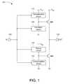
- FIG. 1is a block diagram of a circuit in accordance with one embodiment of the present invention.
- FIG. 2is a voltage versus time graph illustrating slew rate adjustments for one embodiment of the drive transistor of the circuit of FIG. 1;
- FIG. 3is a circuit diagram of one embodiment of the circuit of FIG. 1;
- FIG. 4is a circuit diagram of a bias circuit used in one embodiment of the circuit of FIG. 1;
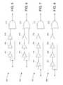
- FIGS. 5 and 6are block diagrams of pulse generators used in one embodiment of the circuit of FIG. 1;
- FIGS. 7 and 8are block diagrams of delay circuits used in one embodiment of the circuit of FIG. 1 .
- present embodimentsare discussed below in the context of an output driver 100 for simplicity only. It is to be understood that present embodiments may be implemented in any circuit, driver, or buffer to maintain a specified slew rate over process and temperature variations. Further, the polarity of control signals and semiconductor devices may be reversed as desired. Also, the specific configurations of various delay circuits, pulse generators, current mirrors, and compensation circuits may be altered as desired. Accordingly, the present invention is not to be construed as limited to specific examples described herein but rather includes within its scope all embodiments defined by the appended claims.
- FIG. 1is a block diagram of a circuit 100 that, in accordance with the present invention, automatically compensates for process and temperature variations its drive transistor(s) to maintain a specified slew rate over such process and temperature variations.
- circuit 100may be used as an output driver, for example, to drive signals between IC chips, where an output signal OUT is driven in response to an input signal IN.
- Circuit 100includes an input 102 , an output 104 , a PMOS drive transistor MP 1 , an NMOS drive transistor MN 1 , compensation circuits 110 and 120 , a pull-down circuit 130 , and a pull-up circuit 140 .
- Input 102receives input signal IN and, in response thereto, drive transistors MP 1 and MN 1 drive output signal OUT on output 104 .
- Circuit 100has a constant output slew rate that does not change with process and/or temperature variations. Specifically, the present invention maintains a specified slew rate for PMOS drive transistor MP 1 over process and temperature variations of transistor MP 1 by adjusting the rate at which its gate discharges during logic low-to-high transitions of output 104 according to those process and temperature variations and, similarly, maintains a specified slew rate for NMOS drive transistor MN 1 over process and temperature variations of transistor MN 1 by adjusting the rate at which its gate charges during logic high-to-low transitions of output 104 according to those process and temperature variations.
- PMOS drive transistor MP 1is coupled between a supply voltage V DD and output 104 , and drives output 104 to a high voltage when IN transitions from logic low to logic high.
- the gate of drive transistor MP 1is coupled between compensation circuit 110 and pull-down circuit 130 , which in turn are coupled in series between V DD and ground potential.
- Compensation circuit 110 and pull-down circuit 130are responsive to IN, and together control the discharge rate of drive transistor MP 1 's gate.
- the slew rate at output 104 for logic low-to-high transitionsis controlled by PMOS drive transistor MP 1 , and is a function of the current, which depends on process and temperature variations, the size of drive transistor MP 1 , and the discharge rate of the gate of drive transistor MP 1 . Discharging the gate of PMOS drive transistor MP 1 at a constant rate will result in a constant slew rate for output 104 during logic low-to-high transitions.
- NMOS drive transistor MN 1is coupled between output 104 and ground potential, and drives output 104 to a low voltage when IN transitions from logic high to logic low.
- the gate of drive transistor MN 1is coupled between pull-down circuit 140 and compensation circuit 120 , which in turn are coupled in series between V DD and ground potential.
- Compensation circuit 120 and pull-down circuit 140are responsive to IN, and together control the charge rate of drive transistor MN 1 's gate.
- the slew rate at output 104 for logic high-to-low transitionsis controlled by drive transistor MN 1 , and is a function of the current, which depends on process and temperature variations, the size of drive transistor MN 1 , and the discharge rate of the gate of drive transistor MN 1 . Charging the gate of NMOS drive transistor MN 1 at a constant rate will result in a constant slew rate for output 104 during logic high-to-low transitions.
- circuit 100The operation of circuit 100 is as follows. When IN transitions from logic low to logic high, NMOS drive transistor MN 1 turns off, for example, using a pull-down circuit (not shown in FIG. 1 for simplicity) coupled between MN 1 's gate and ground potential, although in some embodiments compensation circuit 120 may turn-off transistor MN 1 . Then, pull-down circuit 130 turns on and begins discharging the gate of drive transistor MP 1 toward ground potential. As its gate falls below V DD plus its threshold voltage V T , drive transistor MP 1 turns on and charges output 104 toward V DD to pull signal OUT to logic high. Pull-down circuit 130 discharges MP 1 's gate with a constant current that is substantially independent of process and temperature variations, and thus operates to set up a constant discharge rate for MP 1 's gate over such process and temperature variations.
- a pull-down circuit(not shown in FIG. 1 for simplicity) coupled between MN 1 's gate and ground potential, although in some embodiments compensation circuit 120 may turn-off transistor MN 1 .
- the logic high state of INalso turns on compensation circuit 110 , which in turn slightly adjusts the output slew rate of drive transistor MP 1 according to process and temperature variations therein.
- Compensation circuit 110injects a small compensation current into the gate of drive transistor MP 1 from V DD , thereby canceling some of the discharge current provided by pull-down circuit 130 , and therefore slightly reducing the discharge rate of MP 1 's gate. Because the amount of reduction in the discharge rate of MP 1 's gate is determined by the magnitude of the compensation current, the output slew rate of drive transistor MP 1 may be adjusted for process and temperature variations therein by manipulating the compensation current.
- compensation circuit 110is modeled after and tracks process and temperature variations in drive transistor MP 1 .
- the compensation currentis dependent upon process and temperature variations in drive transistor MP 1 , and automatically adjusts the discharge rate of MP 1 's gate according to process and temperature variations in MP 1 , which in turn maintains the specified low-to-high output slew rate over process and temperature variations in drive transistor MP 1 .
- circuit 100is designed to have a specified slew rate of X volts per second (v/s) for logic low-to-high transitions of output 104 .
- v/svolts per second
- drive transistor 100will pull output 104 from logic low to logic high at the specified slew rate X, as illustrated by line 202 in the graph 200 of FIG. 2 .
- the slew rate Xi.e., slope of line 202
- the net discharge currenti.e., the difference between the compensation current provided by compensation circuit 110 and the discharge current provided by pull-down circuit 130 .
- drive transistor MP 1If, due to process and/or temperature variations, drive transistor MP 1 has a greater drive strength or is otherwise faster than normal, drive transistor MP 1 would be able to more quickly pull output 104 toward V DD , which in turn would result in a greater low-to-high slew rate than specified, as indicated by line 204 in FIG. 2 having a slope of X+ ⁇ .
- compensation circuit 110tracks process and temperature variations in drive transistor MP 1 , compensation circuit 110 will also have a greater drive strength than normal, and therefore will more strongly pull the gate of drive transistor MP 1 toward V DD .
- the greater compensation currentreduces the discharge rate of MP 1 's gate more than normal, which in turn reduces the low-to-high slew rate of output 104 back toward its specified value of X, as indicated in FIG. 2 by arrow 206 .
- compensation circuit 110maintains the specified slew rate for output 104 over process and temperature variations.
- compensation circuit 120 and pull-down circuit 140in maintaining a specified high-to-low slew rate for output 104 over process and temperature variations of drive transistor MN 1 is identical to that described above with respect to PMOS drive transistor MP 1 , with polarities reversed.
- PMOS drive transistor MP 1turns off, for example, using a pull-up circuit (not shown in FIG. 1 for simplicity) coupled between MP 1 's gate and V DD , although in some embodiments compensation circuit 110 may turn off transistor MP 1 .
- pull-up circuit 140begins pulling the gate of drive transistor MN 1 toward V DD .
- drive transistor MN 1turns on and pulls output 104 toward ground potential.
- the charging rate of MN 1 's gateis adjusted for process and temperature variations of drive transistor MN 1 in a manner similar to that described above with respect to compensation circuit 110 and pull-down circuit 120 in order to maintain the specified high-to-low slew rate.
- compensation circuit 120adjusts the magnitude of its compensation current according to process and temperature variations of drive transistor MN 1 to adjust the charging rate of MN 1 's gate in order to compensate for process and temperature variations of drive transistor MN 1 .
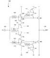
- FIG. 3shows a circuit diagram of a circuit 300 that is one embodiment of circuit 100 of FIG. 1 .
- Input 102is coupled via delay circuit 302 to the input of a CMOS inverter 304 formed by PMOS transistor 306 and NMOS transistor 308 .
- the output of inverter 304is coupled to the gate of PMOS drive transistor MP 1 .
- the output of delay circuit 302is also coupled to the gate of a PMOS compensation transistor 114 via a pulse generator 116 .
- PMOS compensation transistor 114 and a PMOS diode-connected transistor 112are coupled in series between V DD and the gate of PMOS drive transistor MP 1 . Together, PMOS transistors 112 and 114 and pulse generator 116 form compensation circuit 110 of FIG. 1 .
- NMOS pull-down transistor 132is coupled between inverter 304 and ground potential and, in response to a first control voltage provided at node 131 by bias circuit 150 , provides a constant current that is substantially independent of process and temperature variations. Together, pull-down transistor 132 and bias circuit 150 form pull-down circuit 130 of FIG. 1 .
- compensation circuit 110generates a current that is dependent upon process and temperature variations of PMOS drive transistor MP 1 .
- pulse generator 116when input 102 transitions from logic low to logic high, pulse generator 116 generates a pulse that turns on compensation transistor 114 , which in turn injects current into the gate of drive transistor MP 1 from V DD through diode 112 , thereby effectively canceling some of the discharge current provided by pull-down transistor 132 .
- the net discharge currentwill discharge MP 1 's gate at a constant rate.
- Diode-connected transistor 112provides a voltage drop from V DD to reduce the voltage applied across compensation transistor 114 , and in some embodiments may be eliminated.
- PMOS compensation transistor 114is modeled after drive transistor MP 1 .
- PMOS compensation transistor 114is much smaller than PMOS drive transistor MP 1 in order to effectively track process and temperature variations in drive transistor MP 1 .
- PMOS drive transistor MP 1is relatively weak due to process and/or temperature variations
- PMOS compensation transistor 114 and PMOS diode 112are also relatively weak, and therefore provide a smaller compensation current.
- the smaller compensation currentresults in a larger net current for discharging MP 1 's gate, which in turn increases the slew rate of output 104 back to its specified value.
- PMOS compensation transistor 114 and PMOS diode 112are also relatively strong, and therefore provide a larger compensation current.
- the larger compensation currentresults in a smaller net current for discharging MP 1 's gate, which in turn decreases the slew rate of output 104 back to its specified value.
- PMOS compensation transistor 114maintains the specified low-to-high slew rate for output 104 over process and temperature variations of PMOS drive transistor MP 1 .
- Pulse generator 116generates a pulse whose width is approximately equal to the rising time of the voltage at output 104 so that compensation transistor 114 is conductive only during this period of time.
- pulse generator 116advantageously saves power consumption, and allows the gate of PMOS drive transistor MP 1 to be fully discharged to ground.
- pulse generator 116may be eliminated.
- FIG. 5shows a pulse generator 500 that is one embodiment of pulse generator 116 of FIG. 3 .
- Pulse generator 500includes inverters 501 - 503 coupled between delay circuit 302 and a first input of a NAND gate 510 , which has a second input coupled to delay circuit 302 and an output to provide the pulse to compensation transistor 114 .
- the duration of the pulseis determined by the gate delays of inverters 501 - 503 , which may be conventional CMOS inverters, and NAND gate 510 .
- Input 102is also coupled via delay circuit 310 to the input of a CMOS inverter 312 formed by PMOS transistor 314 and NMOS transistor 316 .
- the output of inverter 312is coupled to the gate of NMOS drive transistor MN 1 .
- the output of delay circuit 310is also coupled to the gate of an NMOS compensation transistor 124 via a pulse generator 126 .
- NMOS compensation transistor 124 and an NMOS diode-connected transistor 122are coupled in series between the gate of NMOS drive transistor MN 1 and ground potential. Together, NMOS transistors 122 and 124 and pulse generator 126 form compensation circuit 120 of FIG. 1 .
- PMOS pull-up transistor 142is coupled between inverter 312 and V DD and, in response to a second control voltage provided at node 141 by bias circuit 150 , provides a constant. Together, pull-up transistor 142 and bias circuit 150 form pull-up circuit 140 of FIG. 1 .
- Compensation circuit 120generates a current that is dependent upon process and temperature variations of NMOS drive transistor MN 1 .
- pulse generator 126When input 102 transitions from logic high to logic low, pulse generator 126 generates a pulse that turns on compensation transistor 124 , which in turn draws current from the gate of drive transistor MP 1 toward ground potential through NMOS diode 122 , thereby effectively canceling some of the charge current provided by pull-up transistor 142 .
- the net current between the charge and compensation currentswill charge the gate of drive transistor MN 1 at a constant rate.
- NMOS diode-connected transistor 122provides a voltage drop above ground potential to reduce the voltage applied across NMOS compensation transistor 124 , and in some embodiments may be eliminated.
- NMOS compensation transistor 124is modeled after drive transistor MN 1 in order to compensate for process and temperature variations of drive transistor MN 1 .
- NMOS compensation transistor 124is much smaller than NMOS drive transistor MN 1 in order to effectively track process and temperature variations in drive transistor MN 1 .
- NMOS drive transistor MN 1is relatively weak due to process and/or temperature variations
- NMOS compensation transistor 124 and NMOS diode 122are also relatively weak, and therefore provide a smaller compensation current.
- the smaller compensation currentresults in a larger net current for charging MN 1 's gate, which in turn increases the high-to-low slew rate of output 104 back to its specified value.
- NMOS compensation transistor 124 and NMOS diode 122are also relatively strong, and therefore provide a larger compensation current.
- the larger compensation currentresults in a smaller net current for charging MN 1 's gate, which in turn decreases the high-to-low slew rate of output 104 back to its specified value.
- NMOS compensation transistor 124maintains the specified output slew rate for NMOS drive transistor MN 1 over process and temperature variations of NMOS drive transistor MN 1 .
- Pulse generator 126generates a pulse whose width is approximately equal to the falling time of the voltage at output 104 so that compensation transistor 124 is conductive only during this time period.
- pulse generator 126advantageously saves power consumption, and allows the gate of NMOS drive transistor MN 1 to be fully charged to V DD .
- pulse generator 126may be eliminated.
- FIG. 6shows a pulse generator 600 that is one embodiment of pulse generator 126 of FIG. 3 .
- Pulse generator 600includes inverters 601 - 603 coupled between delay circuit 310 and a first input of a NOR gate 610 , which has a second input coupled to delay circuit 310 and an output to provide the pulse to compensation transistor 124 .
- the duration of the pulseis determined by the gate delays of inverters 601 - 603 , which may be conventional CMOS inverters, and NOR gate 610 .
- FIG. 4shows a bias circuit 400 that is one embodiment of bias circuit 150 of FIG. 3 .
- Bias circuit 400has a voltage-to-current converter including an operational amplifier 401 , an NMOS conversion transistor 402 , and a resistor 403 , and has a current mirror including PMOS transistors. 404 - 406 and NMOS transistors 407 - 408 . Together, the voltage-to-current converter and the current mirror provide gate voltages at nodes 131 and 141 that maintain constant currents through pull-down transistor 132 and pull-up transistor 142 , respectively, irrespective of process and temperature variations.
- Op-amp 401includes a non-inverting input coupled to a reference voltage V REF , an inverting input coupled between transistor 402 and resistor 403 , and an output coupled to the gate of transistor 402 .
- V REF and resistor 403are provided off-chip to ensure more accurate values.
- Op-amp 401amplifies the voltage difference between its inverting and non-inverting inputs to produce a gate voltage for conversion transistor 402 , which in response thereto provides a constant current through resistor 403 that has a value given by I 1 ⁇ V REF /R, where R is the resistance of resistor 403 .
- transistor 402If, due to process and temperature variations, transistor 402 produces more current than normal in response to the same gate-to-source voltage, the current I 1 through resistor 403 increases accordingly.
- the higher current I 1increases the voltage drop across resistor 403 , which in turn causes the voltage at op-amp 401 's inverting terminal to increase, thereby reducing the voltage differential at op-amp 401 's inputs.
- op-amp 401reduces the gate voltage of transistor 402 , which in turn reduces the current I 1 through resistor 403 .
- the negative feedback loop provided by transistor 402 and resistor 403maintains a constant current I 1 through resistor 403 that is substantially independent of process and temperature variations.
- PMOS transistor 404conducts current I 1 , and is connected to PMOS transistors 405 and 406 as a current mirror.
- PMOS transistors 405 and 406will conduct currents I 2 and I 3 , respectively, that are equal to I 1 .
- NMOS transistors 407 and 408are connected as a current mirror, and also conduct currents I 2 and I 3 , respectively, if they are similarly sized. Because the current I 1 is compensated for process and temperature variations, the currents I 2 and I 3 are also compensated for process and temperature variations.
- NMOS transistor 407is coupled to the gate of NMOS pull-down transistor 132 via node 131 , pull-down transistor 132 mirrors the current I 2 , and therefore discharges the gate of PMOS drive transistor MP 1 at a constant rate over process and temperature variations.
- the gate of PMOS transistor 406is coupled to the gate of PMOS pull-up transistor 142 via node 141 , pull-up transistor 142 mirrors the current I 3 , and therefore charges the gate of NMOS drive transistor MN 1 at a constant rate over process and temperature variations.
- delay circuits 302 and 310are conventional delay elements that prevent a short circuit through drive transistors MP 1 and MN 1 by ensuring that during logic low-to-high transitions inverter 304 causes PMOS drive transistor MP 1 to turn on after inverter 312 causes NMOS drive transistor MN 1 to turn off and, conversely, that during logic high-to-low transitions, inverter 312 causes drive transistor MN 1 to turn on after inverter 304 causes drive transistor MP 1 to turn off.
- Delay circuits 302 and 312may be conventional, and the delays provided thereby may be adjusted as desired to prevent a short circuit in the drive transistors MP 1 and MN 1 . For one embodiment, delay circuits 302 and 310 may be eliminated.
- FIG. 7shows a delay circuit 700 that is one embodiment of delay circuit 302 .
- Delay circuit 700includes four inverters 701 - 704 coupled between input 102 and a first input of an AND gate 710 , which has a second input coupled to input 102 and an output coupled to inverter 304 .
- Delay circuit 700delays logic low-to-high transitions at the input of inverter 304 by an amount determined by the propagation delays of its inverters 701 - 704 .
- FIG. 8shows a delay circuit 800 that is one embodiment of delay circuit 310 .
- Delay circuit 800includes four inverters 701 - 704 coupled between input 102 and a first input of an OR gate 810 , which has a second input coupled to input 102 and an output coupled to inverter 312 .
- Delay circuit 800delays logic high-to-low transitions at the input of inverter 312 by an amount determined by the propagation delays of its inverters 801 - 804 .
Landscapes
- Physics & Mathematics (AREA)
- Engineering & Computer Science (AREA)
- Computer Hardware Design (AREA)
- Computing Systems (AREA)
- General Engineering & Computer Science (AREA)
- Mathematical Physics (AREA)
- Logic Circuits (AREA)
- Electronic Switches (AREA)
Abstract
Description
1. Field of Invention
This invention relates generally to digital logic systems and specifically to maintaining specified performance characteristics over process and temperature variations.
2. Description of Related Art
Modern electronic devices such as personal computers typically include a plurality of integrated circuit (IC) or semiconductor chips that communicate with each other, for example, via a common bus. Typically, each IC chip includes an output driver to drive signals from the IC chip onto the bus, or alternately, directly onto one or more other IC chips. The rate at which an output driver transitions a signal (e.g., logic low to logic high) is known as its slew rate, which is typically measured in volts per unit of time. In order to ensure circuit speed compatibility between IC chips and associated buses, the output drivers used in the IC chips should adhere to a specified slew rate range. If the specified slew rate is not met by an output driver, its host IC chip may not operate at the specified frequency, and may become incompatible with other chips or devices. Further, although higher operating frequencies are generally desired, if the slew rate is too high, e.g., the output driver charges the output signal too quickly, undesirable noise may be introduced into the output signal. As a result, it is important for the output drivers to maintain the specified slew rate at all times.
Conventional output drivers have several limitations.
First, as the physical dimensions of IC chips become smaller, it becomes more difficult to control the operating characteristics (e.g., slew rates) of the transistors therein. Process variations inherent in the fabrication of semiconductor chips often cause transistors of the same design to behave differently. For example, the amount of current provided by a transistor, which affects its slew rate, is dependent upon a number of factors including, for example, transistor size, gate-to-source voltage (VGS), and manufacturing-related parameters. Although transistor size and VGSmay be precisely controlled, manufacturing process characteristics typically vary between transistors because, for example, of imperfections in available doping technologies. Indeed, because implant doping is a chemical process performed over time, variations in dopant concentrations between transistors, especially between transistors fabricated from different wafers, are inevitable. These variations are even more pronounced for smaller devices, and may result in significant operating characteristic variations. As a result, output drivers of the same design and having the same specified operating characteristics may undesirably operate at different speeds, and therefore may have slew rates different from those specified.
Further, transistor operating characteristics vary with changes in temperature. Typically, transistors tend to operate more slowly as the IC chip heats up and, conversely, tend to operate more quickly as the IC chip cools down. As a result, the slew rate of conventional output drivers undesirably varies with temperature. Accordingly, changes in the operating temperature of an output driver may cause the output driver's slew rate to drift from its specified slew rate. This, in turn, may lead to unwanted noise and/or incompatibility with other devices.
Thus, there is a need for an improved output driver that maintains a specified slew rate over process and temperature variations of the drive transistor.
A method and apparatus are disclosed that compensate for process and temperature variations in the drive transistor(s) of a circuit in order to maintain a specified slew rate that is independent of such process and temperature variations in the drive transistor(s). In accordance with the present invention, a circuit includes a drive transistor coupled between an output and a first potential, a constant current circuit coupled between the gate of the drive transistor and a second potential, and a compensation circuit coupled between the gate of the drive transistor and the first potential. The constant current circuit uses a constant current that is substantially independent of process and temperature variations to turn on the drive transistor at a constant rate, regardless of process and temperature variations. The compensation circuit provides a small compensation current that cancels some of the constant current and, thus, slightly decreases the turn-on rate of the drive transistor. The compensation current is dependent upon process and temperature variations of the drive transistor, and therefore reduces the turn-on rate of the drive transistor according to process and temperature variations of the drive transistor. In this manner, the output maintains a constant specified slew rate that does not drift in response to process and temperature variations in the drive transistor.
For one embodiment, the drive transistor is a PMOS transistor coupled between an output and a supply voltage, the constant current circuit is an NMOS pull-down transistor coupled between gate of the drive transistor and ground potential, and the compensation circuit is a PMOS transistor coupled between the gate of the drive transistor and the supply voltage. The pull-down transistor, which is controlled by a bias circuit, provides a current that is substantially independent of process and temperature variations, and therefore operates to discharge the gate of the PMOS drive transistor at a constant rate, regardless of process and temperature variations. The compensation transistor conducts a small current that cancels some of the constant current that discharges the gate of the drive transistor. The PMOS compensation transistor models the PMOS drive transistor, and thus tracks process and temperature variations in the drive transistor. Accordingly, the compensation current, which is dependent upon process and temperature variations of the drive transistor, adjusts the discharge rate of the gate of the PMOS drive transistor in response to process and temperature variations therein in order to maintain the specified output slew rate.
For example, if the drive transistor is weaker than normal due to process and/or temperature variations, and thus the output would ordinarily have a lower slew rate than specified, the compensation transistor is also weaker than normal, and thus conducts a weaker compensation current. The weaker compensation current cancels less of the constant discharge current than normal, thereby increasing the discharge rate of the gate of the drive transistor, which in turn increases the output slew rate back toward its specified value. Conversely, if the drive transistor is stronger than normal due to process and/or temperature variations, and thus the output would ordinarily have a higher slew rate than specified, the compensation transistor is also stronger than normal, and thus conducts a stronger compensation current. The stronger compensation current cancels more of the constant discharge current than normal, thereby decreasing the discharge rate of the gate of the drive transistor, which in turn decreases the output slew rate back toward its specified value.
For other embodiments, the drive transistor is an NMOS transistor coupled between the output and ground potential, the constant current circuit is a PMOS pull-up transistor coupled between gate of the drive transistor and the supply voltage, and the compensation circuit is an NMOS transistor coupled between the gate of the drive transistor and ground potential. For such embodiments, the NMOS compensation transistor is modeled after and tracks process and temperature variations in the NMOS drive transistor, thereby adjusting the output slew rate for process and temperature variations in the NMOS drive transistor by effectively canceling an amount of the charge current provided by the pull-up transistor in response to such process and temperature variations.
The features and advantages of the present invention are illustrated by way of example and are by no means intended to limit the scope of the present invention to the particular embodiments shown, and in which:
FIG. 1 is a block diagram of a circuit in accordance with one embodiment of the present invention;
FIG. 2 is a voltage versus time graph illustrating slew rate adjustments for one embodiment of the drive transistor of the circuit of FIG. 1;
FIG. 3 is a circuit diagram of one embodiment of the circuit of FIG. 1;
FIG. 4 is a circuit diagram of a bias circuit used in one embodiment of the circuit of FIG. 1;
FIGS. 5 and 6 are block diagrams of pulse generators used in one embodiment of the circuit of FIG. 1; and
FIGS. 7 and 8 are block diagrams of delay circuits used in one embodiment of the circuit of FIG.1.
Like reference numerals refer to corresponding parts throughout the drawing figures.
Present embodiments are discussed below in the context of anoutput driver 100 for simplicity only. It is to be understood that present embodiments may be implemented in any circuit, driver, or buffer to maintain a specified slew rate over process and temperature variations. Further, the polarity of control signals and semiconductor devices may be reversed as desired. Also, the specific configurations of various delay circuits, pulse generators, current mirrors, and compensation circuits may be altered as desired. Accordingly, the present invention is not to be construed as limited to specific examples described herein but rather includes within its scope all embodiments defined by the appended claims.
FIG. 1 is a block diagram of acircuit 100 that, in accordance with the present invention, automatically compensates for process and temperature variations its drive transistor(s) to maintain a specified slew rate over such process and temperature variations. For one embodiment,circuit 100 may be used as an output driver, for example, to drive signals between IC chips, where an output signal OUT is driven in response to an input signal IN.Circuit 100 includes aninput 102, anoutput 104, a PMOS drive transistor MP1, an NMOS drive transistor MN1,compensation circuits down circuit 130, and a pull-up circuit 140.Input 102 receives input signal IN and, in response thereto, drive transistors MP1 and MN1 drive output signal OUT onoutput 104.Circuit 100 has a constant output slew rate that does not change with process and/or temperature variations. Specifically, the present invention maintains a specified slew rate for PMOS drive transistor MP1 over process and temperature variations of transistor MP1 by adjusting the rate at which its gate discharges during logic low-to-high transitions ofoutput 104 according to those process and temperature variations and, similarly, maintains a specified slew rate for NMOS drive transistor MN1 over process and temperature variations of transistor MN1 by adjusting the rate at which its gate charges during logic high-to-low transitions ofoutput 104 according to those process and temperature variations.
PMOS drive transistor MP1 is coupled between a supply voltage VDDandoutput 104, and drivesoutput 104 to a high voltage when IN transitions from logic low to logic high. The gate of drive transistor MP1 is coupled betweencompensation circuit 110 and pull-down circuit 130, which in turn are coupled in series between VDDand ground potential.Compensation circuit 110 and pull-down circuit 130 are responsive to IN, and together control the discharge rate of drive transistor MP1's gate. The slew rate atoutput 104 for logic low-to-high transitions is controlled by PMOS drive transistor MP1, and is a function of the current, which depends on process and temperature variations, the size of drive transistor MP1, and the discharge rate of the gate of drive transistor MP1. Discharging the gate of PMOS drive transistor MP1 at a constant rate will result in a constant slew rate foroutput 104 during logic low-to-high transitions.
NMOS drive transistor MN1 is coupled betweenoutput 104 and ground potential, and drivesoutput 104 to a low voltage when IN transitions from logic high to logic low. The gate of drive transistor MN1 is coupled between pull-down circuit 140 andcompensation circuit 120, which in turn are coupled in series between VDDand ground potential.Compensation circuit 120 and pull-down circuit 140 are responsive to IN, and together control the charge rate of drive transistor MN1's gate. The slew rate atoutput 104 for logic high-to-low transitions is controlled by drive transistor MN1, and is a function of the current, which depends on process and temperature variations, the size of drive transistor MN1, and the discharge rate of the gate of drive transistor MN1. Charging the gate of NMOS drive transistor MN1 at a constant rate will result in a constant slew rate foroutput 104 during logic high-to-low transitions.
The operation ofcircuit 100 is as follows. When IN transitions from logic low to logic high, NMOS drive transistor MN1 turns off, for example, using a pull-down circuit (not shown in FIG. 1 for simplicity) coupled between MN1's gate and ground potential, although in someembodiments compensation circuit 120 may turn-off transistor MN1. Then, pull-down circuit 130 turns on and begins discharging the gate of drive transistor MP1 toward ground potential. As its gate falls below VDDplus its threshold voltage VT, drive transistor MP1 turns on andcharges output 104 toward VDDto pull signal OUT to logic high. Pull-down circuit 130 discharges MP1's gate with a constant current that is substantially independent of process and temperature variations, and thus operates to set up a constant discharge rate for MP1's gate over such process and temperature variations.
The logic high state of IN also turns oncompensation circuit 110, which in turn slightly adjusts the output slew rate of drive transistor MP1 according to process and temperature variations therein.Compensation circuit 110 injects a small compensation current into the gate of drive transistor MP1 from VDD, thereby canceling some of the discharge current provided by pull-down circuit 130, and therefore slightly reducing the discharge rate of MP1's gate. Because the amount of reduction in the discharge rate of MP1's gate is determined by the magnitude of the compensation current, the output slew rate of drive transistor MP1 may be adjusted for process and temperature variations therein by manipulating the compensation current. Specifically,compensation circuit 110 is modeled after and tracks process and temperature variations in drive transistor MP1. Thus, the compensation current is dependent upon process and temperature variations in drive transistor MP1, and automatically adjusts the discharge rate of MP1's gate according to process and temperature variations in MP1, which in turn maintains the specified low-to-high output slew rate over process and temperature variations in drive transistor MP1.
For example, supposecircuit 100 is designed to have a specified slew rate of X volts per second (v/s) for logic low-to-high transitions ofoutput 104. Thus, if there are no process variations in the fabrication ofcircuit 100, and no temperature variations during operation ofcircuit 100,drive transistor 100 will pulloutput 104 from logic low to logic high at the specified slew rate X, as illustrated byline 202 in the graph200 of FIG.2. As mentioned above, the slew rate X (i.e., slope of line202) is determined by the net discharge current, i.e., the difference between the compensation current provided bycompensation circuit 110 and the discharge current provided by pull-down circuit 130. If, due to process and/or temperature variations, drive transistor MP1 has a greater drive strength or is otherwise faster than normal, drive transistor MP1 would be able to more quickly pulloutput 104 toward VDD, which in turn would result in a greater low-to-high slew rate than specified, as indicated byline 204 in FIG. 2 having a slope of X+Δ.
Becausecompensation circuit 110 tracks process and temperature variations in drive transistor MP1,compensation circuit 110 will also have a greater drive strength than normal, and therefore will more strongly pull the gate of drive transistor MP1 toward VDD. The greater compensation current reduces the discharge rate of MP1's gate more than normal, which in turn reduces the low-to-high slew rate ofoutput 104 back toward its specified value of X, as indicated in FIG. 2 byarrow 206.
Conversely, if drive transistor MP1 is weaker than normal because of process and/or temperature variations,output 104 would otherwise have a lower slew rate than specified, as indicated byline 208 in FIG. 2 having a slope of X−Δ. Consequently,compensation circuit 110 will also have a lower drive strength than normal, and therefore will produce a lower compensation current than normal. The lower compensation current will not decrease the discharge rate of MP1's gate as much as normal, which in turn will increase the slew rate ofoutput 104 back to its specified value of X, as indicated byarrow 210.
Therefore, by adjusting the discharge rate of MP1's gate in response to process and temperature variations therein,compensation circuit 110 maintains the specified slew rate foroutput 104 over process and temperature variations.
The operation ofcompensation circuit 120 and pull-down circuit 140 in maintaining a specified high-to-low slew rate foroutput 104 over process and temperature variations of drive transistor MN1 is identical to that described above with respect to PMOS drive transistor MP1, with polarities reversed. Thus, for example, when IN transitions from logic high to logic low, PMOS drive transistor MP1 turns off, for example, using a pull-up circuit (not shown in FIG. 1 for simplicity) coupled between MP1's gate and VDD, although in someembodiments compensation circuit 110 may turn off transistor MP1. Then, pull-upcircuit 140 begins pulling the gate of drive transistor MN1 toward VDD. As its gate voltage reaches its VT, drive transistor MN1 turns on and pullsoutput 104 toward ground potential. The charging rate of MN1's gate is adjusted for process and temperature variations of drive transistor MN1 in a manner similar to that described above with respect tocompensation circuit 110 and pull-down circuit 120 in order to maintain the specified high-to-low slew rate. Thus,compensation circuit 120 adjusts the magnitude of its compensation current according to process and temperature variations of drive transistor MN1 to adjust the charging rate of MN1's gate in order to compensate for process and temperature variations of drive transistor MN1.
FIG. 3 shows a circuit diagram of acircuit 300 that is one embodiment ofcircuit 100 of FIG.1.Input 102 is coupled viadelay circuit 302 to the input of aCMOS inverter 304 formed byPMOS transistor 306 andNMOS transistor 308. The output ofinverter 304 is coupled to the gate of PMOS drive transistor MP1. The output ofdelay circuit 302 is also coupled to the gate of aPMOS compensation transistor 114 via apulse generator 116.PMOS compensation transistor 114 and a PMOS diode-connected transistor112 are coupled in series between VDDand the gate of PMOS drive transistor MP1. Together,PMOS transistors 112 and114 andpulse generator 116form compensation circuit 110 of FIG.1. NMOS pull-down transistor 132 is coupled betweeninverter 304 and ground potential and, in response to a first control voltage provided atnode 131 bybias circuit 150, provides a constant current that is substantially independent of process and temperature variations. Together, pull-down transistor 132 andbias circuit 150 form pull-down circuit 130 of FIG.1.
As described above,compensation circuit 110 generates a current that is dependent upon process and temperature variations of PMOS drive transistor MP1. Specifically, wheninput 102 transitions from logic low to logic high,pulse generator 116 generates a pulse that turns oncompensation transistor 114, which in turn injects current into the gate of drive transistor MP1 from VDDthrough diode112, thereby effectively canceling some of the discharge current provided by pull-down transistor 132. The net discharge current will discharge MP1's gate at a constant rate. Diode-connected transistor112 provides a voltage drop from VDDto reduce the voltage applied acrosscompensation transistor 114, and in some embodiments may be eliminated.
In order to compensate for process and temperature variations of drive transistor MP1,PMOS compensation transistor 114 is modeled after drive transistor MP1. In one embodiment,PMOS compensation transistor 114 is much smaller than PMOS drive transistor MP1 in order to effectively track process and temperature variations in drive transistor MP1. Thus, if PMOS drive transistor MP1 is relatively weak due to process and/or temperature variations,PMOS compensation transistor 114 and PMOS diode112 are also relatively weak, and therefore provide a smaller compensation current. The smaller compensation current results in a larger net current for discharging MP1's gate, which in turn increases the slew rate ofoutput 104 back to its specified value. Conversely, if PMOS drive transistor MP1 is relatively strong due to process and/or temperature variations,PMOS compensation transistor 114 and PMOS diode112 are also relatively strong, and therefore provide a larger compensation current. The larger compensation current results in a smaller net current for discharging MP1's gate, which in turn decreases the slew rate ofoutput 104 back to its specified value. In this manner,PMOS compensation transistor 114 maintains the specified low-to-high slew rate foroutput 104 over process and temperature variations of PMOS drive transistor MP1.
FIG. 5 shows apulse generator 500 that is one embodiment ofpulse generator 116 of FIG.3.Pulse generator 500 includes inverters501-503 coupled betweendelay circuit 302 and a first input of aNAND gate 510, which has a second input coupled to delaycircuit 302 and an output to provide the pulse tocompensation transistor 114. The duration of the pulse is determined by the gate delays of inverters501-503, which may be conventional CMOS inverters, andNAND gate 510.
FIG. 6 shows apulse generator 600 that is one embodiment ofpulse generator 126 of FIG.3.Pulse generator 600 includes inverters601-603 coupled betweendelay circuit 310 and a first input of a NORgate 610, which has a second input coupled to delaycircuit 310 and an output to provide the pulse tocompensation transistor 124. The duration of the pulse is determined by the gate delays of inverters601-603, which may be conventional CMOS inverters, and NORgate 610.
FIG. 4 shows abias circuit 400 that is one embodiment ofbias circuit 150 of FIG.3.Bias circuit 400 has a voltage-to-current converter including anoperational amplifier 401, anNMOS conversion transistor 402, and aresistor 403, and has a current mirror including PMOS transistors.404-406 and NMOS transistors407-408. Together, the voltage-to-current converter and the current mirror provide gate voltages atnodes down transistor 132 and pull-uptransistor 142, respectively, irrespective of process and temperature variations.
Op-amp 401 includes a non-inverting input coupled to a reference voltage VREF, an inverting input coupled betweentransistor 402 andresistor 403, and an output coupled to the gate oftransistor 402. For one embodiment, VREFandresistor 403 are provided off-chip to ensure more accurate values. Op-amp 401 amplifies the voltage difference between its inverting and non-inverting inputs to produce a gate voltage forconversion transistor 402, which in response thereto provides a constant current throughresistor 403 that has a value given by I1≈VREF/R, where R is the resistance ofresistor 403. If, due to process and temperature variations,transistor 402 produces more current than normal in response to the same gate-to-source voltage, the current I1throughresistor 403 increases accordingly. The higher current I1increases the voltage drop acrossresistor 403, which in turn causes the voltage at op-amp 401's inverting terminal to increase, thereby reducing the voltage differential at op-amp 401's inputs. As a result, op-amp 401 reduces the gate voltage oftransistor 402, which in turn reduces the current I1throughresistor 403. In this manner, the negative feedback loop provided bytransistor 402 andresistor 403 maintains a constant current I1throughresistor 403 that is substantially independent of process and temperature variations.
Referring again to FIG. 3, delaycircuits high transitions inverter 304 causes PMOS drive transistor MP1 to turn on afterinverter 312 causes NMOS drive transistor MN1 to turn off and, conversely, that during logic high-to-low transitions,inverter 312 causes drive transistor MN1 to turn on afterinverter 304 causes drive transistor MP1 to turn off. Delaycircuits circuits
FIG. 7 shows adelay circuit 700 that is one embodiment ofdelay circuit 302.Delay circuit 700 includes four inverters701-704 coupled betweeninput 102 and a first input of an ANDgate 710, which has a second input coupled to input102 and an output coupled toinverter 304.Delay circuit 700 delays logic low-to-high transitions at the input ofinverter 304 by an amount determined by the propagation delays of its inverters701-704.
FIG. 8 shows adelay circuit 800 that is one embodiment ofdelay circuit 310.Delay circuit 800 includes four inverters701-704 coupled betweeninput 102 and a first input of anOR gate 810, which has a second input coupled to input102 and an output coupled toinverter 312.Delay circuit 800 delays logic high-to-low transitions at the input ofinverter 312 by an amount determined by the propagation delays of its inverters801-804.
While particular embodiments of the present invention have been shown and described, it will be obvious to those skilled in the art that changes and modifications may be made without departing from this invention in its broader aspects and, therefore, the appended claims are to encompass within their scope all such changes and modifications as fall within the true spirit and scope of this invention.
Claims (27)
1. A circuit for maintaining a specified slew rate over process and temperature variations, comprising:
a drive transistor coupled between a first potential and an output of the circuit;
a first transistor coupled between a gate of the drive transistor and a second potential, the first transistor responsive to an input signal, and operative to pull the gate voltage of the drive transistor toward the second potential at a constant rate during a logic transition of the input signal to turn on the drive transistor;
a current source coupled between the first transistor and the second potential, the current source for generating a constant current that is substantially independent of process and temperature variations; and
a compensation transistor coupled between the gate of the drive transistor and the first potential, the compensation transistor responsive to the input signal, and operative to decrease the rate of voltage change of the gate of the drive transistor by an amount dependent upon process and temperature variations in the drive transistor.
2. The circuit ofclaim 1 , further comprising a second transistor coupled between the gate of the drive transistor and the first potential, the second transistor being responsive to the complement of the input signal.
3. The circuit ofclaim 1 , further comprising a pulse generator coupled to the gate of the compensation transistor.
4. The circuit ofclaim 3 , wherein the pulse generator generates a pulse having a width approximately equal to the transition time of the output.
5. The circuit ofclaim 1 , wherein the compensation transistor models the drive transistor such that process and temperature variations in the compensation transistor track process and temperature variations in the drive transistor.
6. The circuit ofclaim 5 , wherein the compensation transistor and the drive transistor are the same conductivity type.
7. The circuit ofclaim 1 , further comprising a diode-connected transistor coupled between the compensation transistor and the first potential.
8. A circuit for maintaining a specified slew rate over process and temperature variations, comprising:
a PMOS drive transistor coupled between a supply voltage and an output of the circuit;
a pull-down transistor coupled between a gate of the drive transistor and ground potential, the pull-down transistor providing a discharge current to discharge the gate of the drive transistor during a first logic transition of an input signal in order to turn on the drive transistor at a constant rate;
a first current source coupled between the pull-down transistor and ground potential, the first current source generating a constant current that is substantially independent of process and temperature variations; and
a PMOS compensation transistor coupled between the gate of the PMOS drive transistor and the supply voltage, the PMOS compensation transistor injecting a small compensation current into the gate of the PMOS drive transistor during the first logic transition to reduce the discharge rate of the gate of the PMOS drive transistor by an amount dependent upon process and temperature variations of the PMOS drive transistor.
9. The circuit ofclaim 8 , wherein the pull-down transistor and the compensation transistor are responsive to the input signal.
10. The circuit ofclaim 9 , wherein the PMOS compensation transistor models the PMOS drive transistor such that process and temperature variations in the compensation transistor track process and temperature variations in the PMOS drive transistor.
11. The circuit ofclaim 8 , wherein the compensation current is dependent upon process and temperature variations in the PMOS drive transistor.
12. The circuit ofclaim 8 , further comprising a first pulse generator coupled to the gate of the PMOS compensation transistor.
13. The circuit ofclaim 12 , wherein the first pulse generator generates a pulse whose width is approximately equal to a transition time of the output in response to the first logic transition.
14. The circuit ofclaim 8 , further comprising:
an NMOS drive transistor coupled between the output and ground potential;
a pull-up transistor coupled between a gate of the NMOS drive transistor and the supply voltage, the pull-up transistor providing a charge current to charge the gate of the NMOS drive transistor during a second logic transition of an input signal in order to turn on the NMOS drive transistor at a constant rate; and
an NMOS compensation transistor coupled between the gate of the NMOS drive transistor and ground potential, the NMOS compensation transistor drawing a small compensation current from the gate of the NMOS drive transistor during the second logic transition to reduce the charge rate of the gate of the NMOS drive transistor by an amount dependent upon process and temperature variations of the NMOS drive transistor.
15. The circuit ofclaim 14 , wherein the pull-up transistor and the NMOS compensation transistor are responsive to a complement of the input signal.
16. The circuit ofclaim 14 , further comprising a second current source coupled between the pull-up transistor and the supply voltage, the second current source generating a constant current that is substantially independent of process and temperature variations.
17. The circuit ofclaim 14 , wherein the NMOS compensation transistor models the NMOS drive transistor such that process and temperature variations in the NMOS compensation transistor track process and temperature variations in the NMOS drive transistor.
18. The circuit ofclaim 14 , wherein the compensation current is dependent upon process and temperature variations in the NMOS drive transistor.
19. The circuit ofclaim 14 , further comprising a pulse generator coupled to the gate of the NMOS compensation transistor.
20. The circuit ofclaim 19 , wherein the second pulse generator generates a pulse whose width is approximately equal to a transition time of the output in response to the second logic transition.
21. A circuit for maintaining a specified slew rate over process and temperature variations, comprising:
a drive transistor coupled between a first potential and an output of the circuit;
a first transistor coupled between a gate of the drive transistor and a second potential, the first transistor responsive to an input signal, and operative to pull the gate voltage of the drive transistor toward the second potential at a constant rate during a logic transition of the input signal to turn on the drive transistor;
a compensation transistor coupled between the gate of the drive transistor and the first potential, the compensation transistor responsive to the input signal, and operative to decrease the rate of voltage change of the gate of the drive transistor by an amount dependent upon process and temperature variations in the drive transistor; and
a pulse generator coupled to the gate of the compensation transistor.
22. A circuit for maintaining a specified slew rate over process and temperature variations, comprising:
a drive transistor coupled between a first potential and an output of the circuit;
a current source coupled between a gate of the drive transistor and a second potential, the current source for generating a constant current that is substantially independent of process and temperature variations to pull the gate voltage of the drive transistor toward the second potential at a constant rate during a logic transition of the input signal to turn on the drive transistor; and
a compensation transistor coupled between the gate of the drive transistor and the first potential, the compensation transistor responsive to the input signal, and operative to decrease the rate of voltage change of the gate of the drive transistor by an amount dependent upon process and temperature variations in the drive transistor.
23. The circuit ofclaim 22 , further comprising a first transistor responsive to the input signal and coupled between the current source and the gate of the drive transistor.
24. The circuit ofclaim 22 , further comprising a second transistor responsive to the input signal and coupled between the gate of the drive transistor and the first potential.
25. The circuit ofclaim 22 , further comprising a pulse generator coupled to a gate of the compensation transistor.
26. The circuit ofclaim 25 , wherein the pulse generator generates a pulse whose width is approximately equal to a transition time of the output in response to the logic transition.
27. The circuit ofclaim 22 , further comprising a diode-connected transistor coupled between the compensation transistor and the first potential.
Priority Applications (1)
| Application Number | Priority Date | Filing Date | Title |
|---|---|---|---|
| US10/024,884US6535020B1 (en) | 2001-12-18 | 2001-12-18 | Output buffer with compensated slew rate and delay control |
Applications Claiming Priority (1)
| Application Number | Priority Date | Filing Date | Title |
|---|---|---|---|
| US10/024,884US6535020B1 (en) | 2001-12-18 | 2001-12-18 | Output buffer with compensated slew rate and delay control |
Publications (1)
| Publication Number | Publication Date |
|---|---|
| US6535020B1true US6535020B1 (en) | 2003-03-18 |
Family
ID=21822864
Family Applications (1)
| Application Number | Title | Priority Date | Filing Date |
|---|---|---|---|
| US10/024,884Expired - LifetimeUS6535020B1 (en) | 2001-12-18 | 2001-12-18 | Output buffer with compensated slew rate and delay control |
Country Status (1)
| Country | Link |
|---|---|
| US (1) | US6535020B1 (en) |
Cited By (55)
| Publication number | Priority date | Publication date | Assignee | Title |
|---|---|---|---|---|
| US20030090293A1 (en)* | 2001-11-14 | 2003-05-15 | Via Technologies, Inc. | I/O buffer with variable conductivity |
| US20030164723A1 (en)* | 2002-03-04 | 2003-09-04 | Fujitsu Limited | Output buffer circuit |
| US6690192B1 (en)* | 2002-10-16 | 2004-02-10 | Pericom Semiconductor Corp. | Current-compensated CMOS output buffer adjusting edge rate for process, temperature, and Vcc variations |
| US20040046601A1 (en)* | 2002-09-10 | 2004-03-11 | Samsung Electronics Co., Ltd. | Circuit with fuse and semiconductor device having the same circuit |
| US6756826B1 (en)* | 2003-06-12 | 2004-06-29 | Fairchild Semiconductor Corporation | Method of reducing the propagation delay and process and temperature effects on a buffer |
| US20040151032A1 (en)* | 2003-01-30 | 2004-08-05 | Yan Polansky | High speed and low noise output buffer |
| US20050040866A1 (en)* | 2001-11-27 | 2005-02-24 | Janssen Hendrikus Johannes | Output driver comprising an improved control circuit |
| US20050046406A1 (en)* | 2003-09-02 | 2005-03-03 | Paolo Menegoli | Process insensitive voltage reference |
| US20060034122A1 (en)* | 2004-08-12 | 2006-02-16 | Yoram Betser | Dynamic matching of signal path and reference path for sensing |
| US20060056240A1 (en)* | 2004-04-01 | 2006-03-16 | Saifun Semiconductors, Ltd. | Method, circuit and system for erasing one or more non-volatile memory cells |
| US20060068551A1 (en)* | 2004-09-27 | 2006-03-30 | Saifun Semiconductors, Ltd. | Method for embedding NROM |
| US20060214688A1 (en)* | 2005-03-22 | 2006-09-28 | Micron Technology, Inc. | Output buffer and method having a supply voltage insensitive slew rate |
| US20060285408A1 (en)* | 2005-06-17 | 2006-12-21 | Saifun Semiconductors, Ltd. | Method circuit and system for compensating for temperature induced margin loss in non-volatile memory cells |
| US20060285386A1 (en)* | 2005-06-15 | 2006-12-21 | Saifun Semiconductors, Ltd. | Accessing an NROM array |
| US20070018684A1 (en)* | 2004-07-20 | 2007-01-25 | Dong Pan | Temperature-compensated output buffer |
| US20070036007A1 (en)* | 2005-08-09 | 2007-02-15 | Saifun Semiconductors, Ltd. | Sticky bit buffer |
| US20070035180A1 (en)* | 2005-07-07 | 2007-02-15 | Seong-Jin Jang | Line driver circuit having means for stabilizing output signal |
| US20070103209A1 (en)* | 2005-11-09 | 2007-05-10 | Hynix Semiconductor Inc. | Apparatus and method for outputting data of semiconductor memory apparatus |
| US7221138B2 (en) | 2005-09-27 | 2007-05-22 | Saifun Semiconductors Ltd | Method and apparatus for measuring charge pump output current |
| US7317633B2 (en) | 2004-07-06 | 2008-01-08 | Saifun Semiconductors Ltd | Protection of NROM devices from charge damage |
| US7352627B2 (en) | 2006-01-03 | 2008-04-01 | Saifon Semiconductors Ltd. | Method, system, and circuit for operating a non-volatile memory array |
| US7369440B2 (en) | 2005-01-19 | 2008-05-06 | Saifun Semiconductors Ltd. | Method, circuit and systems for erasing one or more non-volatile memory cells |
| US7405969B2 (en) | 1997-08-01 | 2008-07-29 | Saifun Semiconductors Ltd. | Non-volatile memory cell and non-volatile memory devices |
| US7420848B2 (en) | 2002-01-31 | 2008-09-02 | Saifun Semiconductors Ltd. | Method, system, and circuit for operating a non-volatile memory array |
| US20080239599A1 (en)* | 2007-04-01 | 2008-10-02 | Yehuda Yizraeli | Clamping Voltage Events Such As ESD |
| US7457183B2 (en) | 2003-09-16 | 2008-11-25 | Saifun Semiconductors Ltd. | Operating array cells with matched reference cells |
| US7512009B2 (en) | 2001-04-05 | 2009-03-31 | Saifun Semiconductors Ltd. | Method for programming a reference cell |
| US7532529B2 (en) | 2004-03-29 | 2009-05-12 | Saifun Semiconductors Ltd. | Apparatus and methods for multi-level sensing in a memory array |
| US7535765B2 (en) | 2004-12-09 | 2009-05-19 | Saifun Semiconductors Ltd. | Non-volatile memory device and method for reading cells |
| US20090128191A1 (en)* | 2005-02-22 | 2009-05-21 | Samsung Electronics Co., Ltd. | Ultra-low-power level shifter, voltage transform circuit and rfid tag including the same |
| US7605579B2 (en) | 2006-09-18 | 2009-10-20 | Saifun Semiconductors Ltd. | Measuring and controlling current consumption and output current of charge pumps |
| US7638835B2 (en) | 2006-02-28 | 2009-12-29 | Saifun Semiconductors Ltd. | Double density NROM with nitride strips (DDNS) |
| US7638850B2 (en) | 2004-10-14 | 2009-12-29 | Saifun Semiconductors Ltd. | Non-volatile memory structure and method of fabrication |
| US7668017B2 (en) | 2005-08-17 | 2010-02-23 | Saifun Semiconductors Ltd. | Method of erasing non-volatile memory cells |
| US7675782B2 (en) | 2002-10-29 | 2010-03-09 | Saifun Semiconductors Ltd. | Method, system and circuit for programming a non-volatile memory array |
| US7692961B2 (en) | 2006-02-21 | 2010-04-06 | Saifun Semiconductors Ltd. | Method, circuit and device for disturb-control of programming nonvolatile memory cells by hot-hole injection (HHI) and by channel hot-electron (CHE) injection |
| US7701779B2 (en) | 2006-04-27 | 2010-04-20 | Sajfun Semiconductors Ltd. | Method for programming a reference cell |
| US7738304B2 (en) | 2002-07-10 | 2010-06-15 | Saifun Semiconductors Ltd. | Multiple use memory chip |
| US7743230B2 (en) | 2003-01-31 | 2010-06-22 | Saifun Semiconductors Ltd. | Memory array programming circuit and a method for using the circuit |
| US20100171727A1 (en)* | 2009-01-06 | 2010-07-08 | Yi-Jan Emry Chen | Output Buffer Circuit with Enhanced Slew Rate |
| US7760554B2 (en) | 2006-02-21 | 2010-07-20 | Saifun Semiconductors Ltd. | NROM non-volatile memory and mode of operation |
| US7786512B2 (en) | 2005-07-18 | 2010-08-31 | Saifun Semiconductors Ltd. | Dense non-volatile memory array and method of fabrication |
| US7808818B2 (en) | 2006-01-12 | 2010-10-05 | Saifun Semiconductors Ltd. | Secondary injection for NROM |
| US20110084745A1 (en)* | 2009-10-13 | 2011-04-14 | Himax Technologies Limited | Output buffer with slew-rate enhancement output stage |
| US20110084733A1 (en)* | 2009-10-13 | 2011-04-14 | Himax Technologies Limited | Driving circuit with slew-rate enhancement circuit |
| CN102034540A (en)* | 2009-09-27 | 2011-04-27 | 上海宏力半导体制造有限公司 | Slew rate control device and method |
| US8053812B2 (en) | 2005-03-17 | 2011-11-08 | Spansion Israel Ltd | Contact in planar NROM technology |
| US8253452B2 (en) | 2006-02-21 | 2012-08-28 | Spansion Israel Ltd | Circuit and method for powering up an integrated circuit and an integrated circuit utilizing same |
| CN102751974A (en)* | 2011-04-22 | 2012-10-24 | 联咏科技股份有限公司 | Output buffer |
| TWI387202B (en)* | 2009-01-05 | 2013-02-21 | Himax Tech Ltd | Output buffer circuit with enhanced slew rate |
| CN103970177A (en)* | 2013-01-29 | 2014-08-06 | 旺宏电子股份有限公司 | Integrated circuit with compensation for manufacturing and environmental variations and method therefor |
| US20160118977A1 (en)* | 2014-10-27 | 2016-04-28 | Texas Instruments Incorporated | Dc-dc converter with temperature, process and voltage compensated dead time delay |
| US20240162814A1 (en)* | 2022-11-16 | 2024-05-16 | Richwave Technology Corp. | Switch device capable of providing a discharge path according to signal level of an input signal |
| US12107572B2 (en) | 2022-12-14 | 2024-10-01 | Richwave Technology Corp. | Switch device where charges accumulated at control terminals of switch units can be discharged and/or neutralized via sub-switch units |
| CN120342380A (en)* | 2025-06-13 | 2025-07-18 | 电子科技大学 | A temperature compensated level shifting driver |
Citations (6)
| Publication number | Priority date | Publication date | Assignee | Title |
|---|---|---|---|---|
| US4857770A (en)* | 1988-02-29 | 1989-08-15 | Advanced Micro Devices, Inc. | Output buffer arrangement for reducing chip noise without speed penalty |
| US5568081A (en) | 1995-06-07 | 1996-10-22 | Cypress Semiconductor, Corporation | Variable slew control for output buffers |
| US5623216A (en)* | 1994-04-22 | 1997-04-22 | Sgs-Thomson Microelectronics S.R.L. | Output buffer current slew rate control integrated circuit |
| US5850159A (en)* | 1997-05-12 | 1998-12-15 | Ind Tech Res Inst | High and low speed output buffer with controlled slew rate |
| US6040737A (en) | 1998-01-09 | 2000-03-21 | S3 Incorporated | Output buffer circuit and method that compensate for operating conditions and manufacturing processes |
| US6064230A (en) | 1998-01-28 | 2000-05-16 | Sun Microsystems, Inc. | Process compensated output driver with slew rate control |
- 2001
- 2001-12-18USUS10/024,884patent/US6535020B1/ennot_activeExpired - Lifetime
Patent Citations (6)
| Publication number | Priority date | Publication date | Assignee | Title |
|---|---|---|---|---|
| US4857770A (en)* | 1988-02-29 | 1989-08-15 | Advanced Micro Devices, Inc. | Output buffer arrangement for reducing chip noise without speed penalty |
| US5623216A (en)* | 1994-04-22 | 1997-04-22 | Sgs-Thomson Microelectronics S.R.L. | Output buffer current slew rate control integrated circuit |
| US5568081A (en) | 1995-06-07 | 1996-10-22 | Cypress Semiconductor, Corporation | Variable slew control for output buffers |
| US5850159A (en)* | 1997-05-12 | 1998-12-15 | Ind Tech Res Inst | High and low speed output buffer with controlled slew rate |
| US6040737A (en) | 1998-01-09 | 2000-03-21 | S3 Incorporated | Output buffer circuit and method that compensate for operating conditions and manufacturing processes |
| US6064230A (en) | 1998-01-28 | 2000-05-16 | Sun Microsystems, Inc. | Process compensated output driver with slew rate control |
Cited By (85)
| Publication number | Priority date | Publication date | Assignee | Title |
|---|---|---|---|---|
| US7405969B2 (en) | 1997-08-01 | 2008-07-29 | Saifun Semiconductors Ltd. | Non-volatile memory cell and non-volatile memory devices |
| US7512009B2 (en) | 2001-04-05 | 2009-03-31 | Saifun Semiconductors Ltd. | Method for programming a reference cell |
| US20030090293A1 (en)* | 2001-11-14 | 2003-05-15 | Via Technologies, Inc. | I/O buffer with variable conductivity |
| US6838906B2 (en)* | 2001-11-14 | 2005-01-04 | Via Technologies, Inc. | I/O buffer with variable conductivity |
| US6956403B2 (en)* | 2001-11-27 | 2005-10-18 | Koninklijke Philips Electronics N.V. | Output drive comprising an improved control circuit |
| US20050040866A1 (en)* | 2001-11-27 | 2005-02-24 | Janssen Hendrikus Johannes | Output driver comprising an improved control circuit |
| US7420848B2 (en) | 2002-01-31 | 2008-09-02 | Saifun Semiconductors Ltd. | Method, system, and circuit for operating a non-volatile memory array |
| US6992511B2 (en)* | 2002-03-04 | 2006-01-31 | Fujitsu Limited | Output buffer circuit |
| US20030164723A1 (en)* | 2002-03-04 | 2003-09-04 | Fujitsu Limited | Output buffer circuit |
| US7738304B2 (en) | 2002-07-10 | 2010-06-15 | Saifun Semiconductors Ltd. | Multiple use memory chip |
| US20040046601A1 (en)* | 2002-09-10 | 2004-03-11 | Samsung Electronics Co., Ltd. | Circuit with fuse and semiconductor device having the same circuit |
| US7116127B2 (en)* | 2002-09-10 | 2006-10-03 | Samsung Electronics Co., Ltd. | Circuit with fuse and semiconductor device having the same circuit |
| US6690192B1 (en)* | 2002-10-16 | 2004-02-10 | Pericom Semiconductor Corp. | Current-compensated CMOS output buffer adjusting edge rate for process, temperature, and Vcc variations |
| US7675782B2 (en) | 2002-10-29 | 2010-03-09 | Saifun Semiconductors Ltd. | Method, system and circuit for programming a non-volatile memory array |
| US20040151032A1 (en)* | 2003-01-30 | 2004-08-05 | Yan Polansky | High speed and low noise output buffer |
| US7743230B2 (en) | 2003-01-31 | 2010-06-22 | Saifun Semiconductors Ltd. | Memory array programming circuit and a method for using the circuit |
| US6756826B1 (en)* | 2003-06-12 | 2004-06-29 | Fairchild Semiconductor Corporation | Method of reducing the propagation delay and process and temperature effects on a buffer |
| US7071673B2 (en)* | 2003-09-02 | 2006-07-04 | Acu Technology Semiconductor Inc. | Process insensitive voltage reference |
| US20050046406A1 (en)* | 2003-09-02 | 2005-03-03 | Paolo Menegoli | Process insensitive voltage reference |
| US7457183B2 (en) | 2003-09-16 | 2008-11-25 | Saifun Semiconductors Ltd. | Operating array cells with matched reference cells |
| US7532529B2 (en) | 2004-03-29 | 2009-05-12 | Saifun Semiconductors Ltd. | Apparatus and methods for multi-level sensing in a memory array |
| US20060056240A1 (en)* | 2004-04-01 | 2006-03-16 | Saifun Semiconductors, Ltd. | Method, circuit and system for erasing one or more non-volatile memory cells |
| US7652930B2 (en) | 2004-04-01 | 2010-01-26 | Saifun Semiconductors Ltd. | Method, circuit and system for erasing one or more non-volatile memory cells |
| US7317633B2 (en) | 2004-07-06 | 2008-01-08 | Saifun Semiconductors Ltd | Protection of NROM devices from charge damage |
| US20070018684A1 (en)* | 2004-07-20 | 2007-01-25 | Dong Pan | Temperature-compensated output buffer |
| US7511531B2 (en)* | 2004-07-20 | 2009-03-31 | Micron Technology, Inc. | Temperature-compensated output buffer |
| US20060034122A1 (en)* | 2004-08-12 | 2006-02-16 | Yoram Betser | Dynamic matching of signal path and reference path for sensing |
| US7095655B2 (en) | 2004-08-12 | 2006-08-22 | Saifun Semiconductors Ltd. | Dynamic matching of signal path and reference path for sensing |
| US7466594B2 (en) | 2004-08-12 | 2008-12-16 | Saifun Semiconductors Ltd. | Dynamic matching of signal path and reference path for sensing |
| US20060068551A1 (en)* | 2004-09-27 | 2006-03-30 | Saifun Semiconductors, Ltd. | Method for embedding NROM |
| US7964459B2 (en) | 2004-10-14 | 2011-06-21 | Spansion Israel Ltd. | Non-volatile memory structure and method of fabrication |
| US7638850B2 (en) | 2004-10-14 | 2009-12-29 | Saifun Semiconductors Ltd. | Non-volatile memory structure and method of fabrication |
| US7535765B2 (en) | 2004-12-09 | 2009-05-19 | Saifun Semiconductors Ltd. | Non-volatile memory device and method for reading cells |
| US7369440B2 (en) | 2005-01-19 | 2008-05-06 | Saifun Semiconductors Ltd. | Method, circuit and systems for erasing one or more non-volatile memory cells |
| US7468926B2 (en) | 2005-01-19 | 2008-12-23 | Saifun Semiconductors Ltd. | Partial erase verify |
| US7834661B2 (en)* | 2005-02-22 | 2010-11-16 | Samsung Electronics Co., Ltd. | Ultra-low-power level shifter, voltage transform circuit and RFID tag including the same |
| US20090128191A1 (en)* | 2005-02-22 | 2009-05-21 | Samsung Electronics Co., Ltd. | Ultra-low-power level shifter, voltage transform circuit and rfid tag including the same |
| US8053812B2 (en) | 2005-03-17 | 2011-11-08 | Spansion Israel Ltd | Contact in planar NROM technology |
| US7795903B2 (en) | 2005-03-22 | 2010-09-14 | Micron Technology, Inc. | Output buffer and method having a supply voltage insensitive slew rate |
| US7528624B2 (en) | 2005-03-22 | 2009-05-05 | Micron Technology, Inc. | Output buffer and method having a supply voltage insensitive slew rate |
| US20060214688A1 (en)* | 2005-03-22 | 2006-09-28 | Micron Technology, Inc. | Output buffer and method having a supply voltage insensitive slew rate |
| US20090201046A1 (en)* | 2005-03-22 | 2009-08-13 | Dong Pan | Output buffer and method having a supply voltage insensitive slew rate |
| US7262637B2 (en) | 2005-03-22 | 2007-08-28 | Micron Technology, Inc. | Output buffer and method having a supply voltage insensitive slew rate |
| US20060285386A1 (en)* | 2005-06-15 | 2006-12-21 | Saifun Semiconductors, Ltd. | Accessing an NROM array |
| US8400841B2 (en) | 2005-06-15 | 2013-03-19 | Spansion Israel Ltd. | Device to program adjacent storage cells of different NROM cells |
| US20060285408A1 (en)* | 2005-06-17 | 2006-12-21 | Saifun Semiconductors, Ltd. | Method circuit and system for compensating for temperature induced margin loss in non-volatile memory cells |
| US7184313B2 (en) | 2005-06-17 | 2007-02-27 | Saifun Semiconductors Ltd. | Method circuit and system for compensating for temperature induced margin loss in non-volatile memory cells |
| US20070035180A1 (en)* | 2005-07-07 | 2007-02-15 | Seong-Jin Jang | Line driver circuit having means for stabilizing output signal |
| US7663413B2 (en)* | 2005-07-07 | 2010-02-16 | Samsung Electronics Co., Ltd. | Line driver circuit having means for stabilizing output signal |
| US7786512B2 (en) | 2005-07-18 | 2010-08-31 | Saifun Semiconductors Ltd. | Dense non-volatile memory array and method of fabrication |
| US20070036007A1 (en)* | 2005-08-09 | 2007-02-15 | Saifun Semiconductors, Ltd. | Sticky bit buffer |
| US7668017B2 (en) | 2005-08-17 | 2010-02-23 | Saifun Semiconductors Ltd. | Method of erasing non-volatile memory cells |
| US7221138B2 (en) | 2005-09-27 | 2007-05-22 | Saifun Semiconductors Ltd | Method and apparatus for measuring charge pump output current |
| US7728641B2 (en)* | 2005-11-09 | 2010-06-01 | Hynix Semiconductor Inc. | Apparatus and method for outputting data of semiconductor memory apparatus |
| US20070103209A1 (en)* | 2005-11-09 | 2007-05-10 | Hynix Semiconductor Inc. | Apparatus and method for outputting data of semiconductor memory apparatus |
| US8508273B2 (en)* | 2005-11-09 | 2013-08-13 | Hynix Semiconductor Inc. | Apparatus and method for outputting data of semiconductor memory apparatus |
| US20100238742A1 (en)* | 2005-11-09 | 2010-09-23 | Hynix Semiconductor Inc. | Apparatus and method for outputting data of semiconductor memory apparatus |
| US7352627B2 (en) | 2006-01-03 | 2008-04-01 | Saifon Semiconductors Ltd. | Method, system, and circuit for operating a non-volatile memory array |
| US7808818B2 (en) | 2006-01-12 | 2010-10-05 | Saifun Semiconductors Ltd. | Secondary injection for NROM |
| US8253452B2 (en) | 2006-02-21 | 2012-08-28 | Spansion Israel Ltd | Circuit and method for powering up an integrated circuit and an integrated circuit utilizing same |
| US7760554B2 (en) | 2006-02-21 | 2010-07-20 | Saifun Semiconductors Ltd. | NROM non-volatile memory and mode of operation |
| US7692961B2 (en) | 2006-02-21 | 2010-04-06 | Saifun Semiconductors Ltd. | Method, circuit and device for disturb-control of programming nonvolatile memory cells by hot-hole injection (HHI) and by channel hot-electron (CHE) injection |
| US7638835B2 (en) | 2006-02-28 | 2009-12-29 | Saifun Semiconductors Ltd. | Double density NROM with nitride strips (DDNS) |
| US7701779B2 (en) | 2006-04-27 | 2010-04-20 | Sajfun Semiconductors Ltd. | Method for programming a reference cell |
| US7605579B2 (en) | 2006-09-18 | 2009-10-20 | Saifun Semiconductors Ltd. | Measuring and controlling current consumption and output current of charge pumps |
| US20080239599A1 (en)* | 2007-04-01 | 2008-10-02 | Yehuda Yizraeli | Clamping Voltage Events Such As ESD |
| TWI387202B (en)* | 2009-01-05 | 2013-02-21 | Himax Tech Ltd | Output buffer circuit with enhanced slew rate |
| US20100171727A1 (en)* | 2009-01-06 | 2010-07-08 | Yi-Jan Emry Chen | Output Buffer Circuit with Enhanced Slew Rate |
| US8289302B2 (en)* | 2009-01-06 | 2012-10-16 | Himax Technologies Limited | Output buffer circuit with enhanced slew rate |
| CN102034540B (en)* | 2009-09-27 | 2013-09-18 | 上海宏力半导体制造有限公司 | Slew rate control device and method |
| CN102034540A (en)* | 2009-09-27 | 2011-04-27 | 上海宏力半导体制造有限公司 | Slew rate control device and method |
| US7969217B2 (en)* | 2009-10-13 | 2011-06-28 | Himax Technologies Limited | Output buffer with slew-rate enhancement output stage |
| US20110084733A1 (en)* | 2009-10-13 | 2011-04-14 | Himax Technologies Limited | Driving circuit with slew-rate enhancement circuit |
| US20110084745A1 (en)* | 2009-10-13 | 2011-04-14 | Himax Technologies Limited | Output buffer with slew-rate enhancement output stage |
| US8022730B2 (en)* | 2009-10-13 | 2011-09-20 | Himax Technologies Limited | Driving circuit with slew-rate enhancement circuit |
| CN102751974B (en)* | 2011-04-22 | 2015-02-25 | 联咏科技股份有限公司 | Output buffer |
| CN102751974A (en)* | 2011-04-22 | 2012-10-24 | 联咏科技股份有限公司 | Output buffer |
| CN103970177A (en)* | 2013-01-29 | 2014-08-06 | 旺宏电子股份有限公司 | Integrated circuit with compensation for manufacturing and environmental variations and method therefor |
| CN103970177B (en)* | 2013-01-29 | 2016-08-10 | 旺宏电子股份有限公司 | Integrated circuit with compensation for manufacturing and environmental variations and method thereof |
| US20160118977A1 (en)* | 2014-10-27 | 2016-04-28 | Texas Instruments Incorporated | Dc-dc converter with temperature, process and voltage compensated dead time delay |
| US9548654B2 (en)* | 2014-10-27 | 2017-01-17 | Texas Instruments Incorporated | DC-DC converter with temperature, process and voltage compensated dead time delay |
| US20240162814A1 (en)* | 2022-11-16 | 2024-05-16 | Richwave Technology Corp. | Switch device capable of providing a discharge path according to signal level of an input signal |
| US12184172B2 (en)* | 2022-11-16 | 2024-12-31 | Richwave Technology Corp. | Switch device capable of providing a discharge path according to signal level of an input signal |
| US12107572B2 (en) | 2022-12-14 | 2024-10-01 | Richwave Technology Corp. | Switch device where charges accumulated at control terminals of switch units can be discharged and/or neutralized via sub-switch units |
| CN120342380A (en)* | 2025-06-13 | 2025-07-18 | 电子科技大学 | A temperature compensated level shifting driver |
Similar Documents
| Publication | Publication Date | Title |
|---|---|---|
| US6535020B1 (en) | Output buffer with compensated slew rate and delay control | |
| US6351172B1 (en) | High-speed output driver with an impedance adjustment scheme | |
| US6975135B1 (en) | Universally programmable output buffer | |
| US5877647A (en) | CMOS output buffer with slew rate control | |
| US7053660B2 (en) | Output buffer circuit and control method therefor | |
| US6094086A (en) | High drive CMOS output buffer with fast and slow speed controls | |
| CN115398804B (en) | Area-efficient slew-rate controlled driver | |
| EP1469603B1 (en) | Slew rate controlled output buffer circuit | |
| US7759992B2 (en) | CML circuit and clock distribution circuit | |
| US6121789A (en) | Output buffer with control circuitry | |
| JPH06112804A (en) | High-speed output buffer circuit for minimization of output signal oscillation and stationary- state current | |
| WO2006078649A1 (en) | Output buffer with slew rate control utilizing an inverse process dependent current reference | |
| US5311084A (en) | Integrated circuit buffer with controlled rise/fall time | |
| US6559676B1 (en) | Output buffer circuit | |
| US6160416A (en) | Full CMOS slew rate controlled input/output buffer | |
| US6850100B2 (en) | Output buffer circuit | |
| KR100686252B1 (en) | Circuit to Reduce Switching Noise | |
| US6380792B1 (en) | Semiconductor integrated circuit | |
| JPH0993111A (en) | Slew rate type buffer circuit | |
| US7009435B2 (en) | Output buffer with controlled slew rate for driving a range of capacitive loads | |
| JP2006526318A (en) | Improved resonant line drive circuit | |
| US6362652B1 (en) | High voltage buffer for submicron CMOS | |
| US6847235B2 (en) | Bus driver | |
| US7242222B2 (en) | Output circuit with reduced gate voltage swings | |
| US6819143B1 (en) | Input buffer circuit having equal duty cycle |
Legal Events
| Date | Code | Title | Description |
|---|---|---|---|
| AS | Assignment | Owner name:SUN MICROSYSTEMS, INC., CALIFORNIA Free format text:ASSIGNMENT OF ASSIGNORS INTEREST;ASSIGNOR:YIN, MING;REEL/FRAME:012397/0344 Effective date:20011212 | |
| FEPP | Fee payment procedure | Free format text:PAYOR NUMBER ASSIGNED (ORIGINAL EVENT CODE: ASPN); ENTITY STATUS OF PATENT OWNER: LARGE ENTITY Free format text:PAYER NUMBER DE-ASSIGNED (ORIGINAL EVENT CODE: RMPN); ENTITY STATUS OF PATENT OWNER: LARGE ENTITY | |
| STCF | Information on status: patent grant | Free format text:PATENTED CASE | |
| FPAY | Fee payment | Year of fee payment:4 | |
| FPAY | Fee payment | Year of fee payment:8 | |
| FPAY | Fee payment | Year of fee payment:12 | |
| AS | Assignment | Owner name:ORACLE AMERICA, INC., CALIFORNIA Free format text:MERGER AND CHANGE OF NAME;ASSIGNORS:ORACLE USA, INC.;SUN MICROSYSTEMS, INC.;ORACLE AMERICA, INC.;REEL/FRAME:037278/0692 Effective date:20100212 |