US6532403B2 - Robot alignment system and method - Google Patents
Robot alignment system and methodDownload PDFInfo
- Publication number
- US6532403B2 US6532403B2US09/837,878US83787801AUS6532403B2US 6532403 B2US6532403 B2US 6532403B2US 83787801 AUS83787801 AUS 83787801AUS 6532403 B2US6532403 B2US 6532403B2
- Authority
- US
- United States
- Prior art keywords
- fine
- target
- alignment
- sensor
- rough
- Prior art date
- Legal status (The legal status is an assumption and is not a legal conclusion. Google has not performed a legal analysis and makes no representation as to the accuracy of the status listed.)
- Expired - Lifetime, expires
Links
- 238000000034methodMethods0.000titleclaimsdescription20
- 239000012636effectorSubstances0.000claimsabstractdescription11
- 238000004891communicationMethods0.000claimsdescription5
- 235000012431wafersNutrition0.000description10
- 230000003287optical effectEffects0.000description5
- 239000004065semiconductorSubstances0.000description4
- 210000005252bulbus oculiAnatomy0.000description3
- 230000004075alterationEffects0.000description2
- 238000010586diagramMethods0.000description2
- 230000001939inductive effectEffects0.000description2
- 238000012986modificationMethods0.000description2
- 230000004048modificationEffects0.000description2
- 230000002596correlated effectEffects0.000description1
- 230000007547defectEffects0.000description1
- 238000005516engineering processMethods0.000description1
- 238000004519manufacturing processMethods0.000description1
- 239000002245particleSubstances0.000description1
- 238000007790scrapingMethods0.000description1
- 238000006748scratchingMethods0.000description1
- 230000002393scratching effectEffects0.000description1
- 230000000007visual effectEffects0.000description1
Images

Classifications
- H—ELECTRICITY
- H01—ELECTRIC ELEMENTS
- H01L—SEMICONDUCTOR DEVICES NOT COVERED BY CLASS H10
- H01L21/00—Processes or apparatus adapted for the manufacture or treatment of semiconductor or solid state devices or of parts thereof
- H01L21/67—Apparatus specially adapted for handling semiconductor or electric solid state devices during manufacture or treatment thereof; Apparatus specially adapted for handling wafers during manufacture or treatment of semiconductor or electric solid state devices or components ; Apparatus not specifically provided for elsewhere
- H01L21/67005—Apparatus not specifically provided for elsewhere
- H01L21/67242—Apparatus for monitoring, sorting or marking
- H01L21/67259—Position monitoring, e.g. misposition detection or presence detection
- H01L21/67265—Position monitoring, e.g. misposition detection or presence detection of substrates stored in a container, a magazine, a carrier, a boat or the like
- B—PERFORMING OPERATIONS; TRANSPORTING
- B25—HAND TOOLS; PORTABLE POWER-DRIVEN TOOLS; MANIPULATORS
- B25J—MANIPULATORS; CHAMBERS PROVIDED WITH MANIPULATION DEVICES
- B25J9/00—Programme-controlled manipulators
- B25J9/16—Programme controls
- B25J9/1694—Programme controls characterised by use of sensors other than normal servo-feedback from position, speed or acceleration sensors, perception control, multi-sensor controlled systems, sensor fusion
- B25J9/1697—Vision controlled systems
- H—ELECTRICITY
- H01—ELECTRIC ELEMENTS
- H01L—SEMICONDUCTOR DEVICES NOT COVERED BY CLASS H10
- H01L21/00—Processes or apparatus adapted for the manufacture or treatment of semiconductor or solid state devices or of parts thereof
- H01L21/67—Apparatus specially adapted for handling semiconductor or electric solid state devices during manufacture or treatment thereof; Apparatus specially adapted for handling wafers during manufacture or treatment of semiconductor or electric solid state devices or components ; Apparatus not specifically provided for elsewhere
- H01L21/683—Apparatus specially adapted for handling semiconductor or electric solid state devices during manufacture or treatment thereof; Apparatus specially adapted for handling wafers during manufacture or treatment of semiconductor or electric solid state devices or components ; Apparatus not specifically provided for elsewhere for supporting or gripping
- H01L21/687—Apparatus specially adapted for handling semiconductor or electric solid state devices during manufacture or treatment thereof; Apparatus specially adapted for handling wafers during manufacture or treatment of semiconductor or electric solid state devices or components ; Apparatus not specifically provided for elsewhere for supporting or gripping using mechanical means, e.g. chucks, clamps or pinches
- H01L21/68707—Apparatus specially adapted for handling semiconductor or electric solid state devices during manufacture or treatment thereof; Apparatus specially adapted for handling wafers during manufacture or treatment of semiconductor or electric solid state devices or components ; Apparatus not specifically provided for elsewhere for supporting or gripping using mechanical means, e.g. chucks, clamps or pinches the wafers being placed on a robot blade, or gripped by a gripper for conveyance
- G—PHYSICS
- G05—CONTROLLING; REGULATING
- G05B—CONTROL OR REGULATING SYSTEMS IN GENERAL; FUNCTIONAL ELEMENTS OF SUCH SYSTEMS; MONITORING OR TESTING ARRANGEMENTS FOR SUCH SYSTEMS OR ELEMENTS
- G05B2219/00—Program-control systems
- G05B2219/30—Nc systems
- G05B2219/37—Measurements
- G05B2219/37558—Optical sensor, scanner
- G—PHYSICS
- G05—CONTROLLING; REGULATING
- G05B—CONTROL OR REGULATING SYSTEMS IN GENERAL; FUNCTIONAL ELEMENTS OF SUCH SYSTEMS; MONITORING OR TESTING ARRANGEMENTS FOR SUCH SYSTEMS OR ELEMENTS
- G05B2219/00—Program-control systems
- G05B2219/30—Nc systems
- G05B2219/39—Robotics, robotics to robotics hand
- G05B2219/39082—Collision, real time collision avoidance
- G—PHYSICS
- G05—CONTROLLING; REGULATING
- G05B—CONTROL OR REGULATING SYSTEMS IN GENERAL; FUNCTIONAL ELEMENTS OF SUCH SYSTEMS; MONITORING OR TESTING ARRANGEMENTS FOR SUCH SYSTEMS OR ELEMENTS
- G05B2219/00—Program-control systems
- G05B2219/30—Nc systems
- G05B2219/40—Robotics, robotics mapping to robotics vision
- G05B2219/40624—Optical beam area sensor
- G—PHYSICS
- G05—CONTROLLING; REGULATING
- G05B—CONTROL OR REGULATING SYSTEMS IN GENERAL; FUNCTIONAL ELEMENTS OF SUCH SYSTEMS; MONITORING OR TESTING ARRANGEMENTS FOR SUCH SYSTEMS OR ELEMENTS
- G05B2219/00—Program-control systems
- G05B2219/30—Nc systems
- G05B2219/45—Nc applications
- G05B2219/45057—Storage handling for disks or material
- G—PHYSICS
- G05—CONTROLLING; REGULATING
- G05B—CONTROL OR REGULATING SYSTEMS IN GENERAL; FUNCTIONAL ELEMENTS OF SUCH SYSTEMS; MONITORING OR TESTING ARRANGEMENTS FOR SUCH SYSTEMS OR ELEMENTS
- G05B2219/00—Program-control systems
- G05B2219/30—Nc systems
- G05B2219/49—Nc machine tool, till multiple
- G05B2219/49114—Go to coarse programmed reference, detector for fine alignment
Definitions
- the present inventionrelates generally to the field of robots and more particularly to a robot alignment system and method.
- Semiconductor wafersare moved into and out of cassettes by automated handling devices (robots) as part of the semiconductor manufacturing process.
- the cassetteshold the wafers while other wafers are being processed.
- the robotsrequire a setup procedure to properly pick up wafers and to properly set wafers into position.
- the setup proceduretypically involves visually determining robot positions and recording these coordinates.
- a number of problemscan occur when robots and platforms are not properly setup. In the most severe case the robots can break wafers. Less severe misalignments can lead to wafer scratching and yield loss. The most common misalignment leads to wafers bumping into the cassette walls and scraping off particles.
- Eyeball alignmentdoes not align to a standard.
- eyeball alignmentscannot address issues related to platform level, robot end effector level, or a dynamic path that the end effector may follow.
- eyeball alignmentsare difficult, time consuming, and inaccurate.
- FIG. 1is a cartoon drawing of a robot alignment system in accordance with one embodiment of the invention
- FIG. 2is a block diagram of a sensor system used in a robot alignment system in accordance with one embodiment of the invention
- FIG. 3is a fine alignment target used in a robot alignment system in accordance with one embodiment of the invention.
- FIG. 4is a flow chart of the steps used in a method of aligning a robot arm in accordance with one embodiment of the invention.
- a robot alignment systemincludes a sensor system.
- the sensor systemis designed to attach to an end effector of a robot arm.
- a rough alignment targetis attached to a work station.
- a fine alignment targetis placed on a work surface of the work station.
- the sensor systemfirst determines the rough alignment target.
- the robot armis then moved to detect the fine alignment target. This system allows the robot arm's motion to be precisely calibrated which significantly reduces the defects to semiconductor wafers.
- FIG. 1is a cartoon drawing of a robot alignment system 10 in accordance with one embodiment of the invention.
- the system 10includes a sensor system 12 that is designed to attach to a robot arm end effector 14 .
- the robot arm 14scans an area so the sensor system can detect a rough alignment target 16 .
- the rough alignment targetsare attached to a work station 16 .
- the informationis passed to a robot controller 18 .
- This informationcan be as simple as a message that a rough alignment target 16 has been detected.
- the robot control 18then records the angle and the height when the message was received.
- the sensor system 12determines the rough angle and the rough height of the target 16 . This information is then communicated with the robot controller.
- the sensor systemdetermines a distance to the target 16 . This information may then be communicated to the controller 18 .
- the arm 14can be extended out to a work cassette 20 on the work station 16 .
- a fine alignment target 22is placed on the work station 16 .
- the sensor system 12detects the fine alignment target 22 .
- the sensor systemcan determine a fine range, a fine angle and fine height.
- the plane of the fine alignment sensorcan be determined. This information is the communicated to the robot controller 18 .
- the rough alignment targets 16are found using a spiral search.
- the robothas already been programmed with the rough alignment of the work stations and the rough alignment targets are not required.
- the sensor systemis placed on the work station where the fine target 22 is shown. The end effector of the robot arm then holds the fine alignment target 22 . This variation can be used to determine if the end effector is drooping.
- the sensor systemcan be any non-contact sensor system, such as optical, capacitive, inductive, sonic.
- optical sensorsare used. An optical beam is shined on the target and the reflection is detected by an optical sensor.
- the targetsare reflectors based on the sensor technology. Distance to the targets can be determined in a number of ways. For instance, the return energy from the target can be correlated to a distance.
- the communication system between the sensor system 12 and the robot controllercan be a RF or other wireless link.
- the communication channelis hard wired and a standard processor to processor protocol is used.
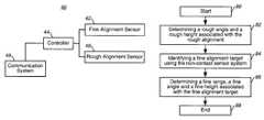
- FIG. 2is a block diagram of a sensor system 40 used in a robot alignment system in accordance with one embodiment of the invention.
- the sensor system 40has a fine alignment sensor 42 .
- the fine alignment sensor 42is connected to a controller 44 .
- a rough alignment sensor 46is also connected to the controller 44 .
- the controller 44is connected to a communication system 48 .
- the fine alignment sensor and the rough alignment sensorare combined in a single sensor.
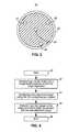
- FIG. 3is a fine alignment target 60 used in a robot alignment system in accordance with one embodiment of the invention.
- the fine alignment target 60has essentially the same shape as a semiconductor wafer.
- An outer ring 62is reflective. The outer ring 62 allows the sensor to know that it has encountered the fine alignment target 60 . Note that the fine alignment target will be described with respect to an optical sensing system, those skilled in the art would know how to modify the target 60 for other sensor systems such as inductive, capacitive or sonic sensors.
- Inside the ring 62are four reflective target zones 64 , 66 , 68 , 70 .
- the target zone 64defines the center of the fine alignment target for the robot.
- the outer target zones 66 , 68 , 70may be used to determine the plane of the fine alignment target 60 .
- the height (fine height)is determined for each of the zones 66 , 68 , 70 . This information with the X-Y (R, ⁇ ) position can be used to define the plane of the fine alignment target.
- FIG. 4is a flow chart of the steps used in a method of aligning a robot arm in accordance with one embodiment of the invention.
- the processstarts, step 80 , by determining a rough angle and a rough height associated with the rough alignment at step 82 .
- a fine alignment targetis identified using the non-contact sensor system at step 84 .
- a fine range, fine angle and a fine height associated with the fine alignment targetis determined which ends the process at step 88 .
- the plane of the fine alignment targetmay also be determined.
- the fine alignment targetis attached to an end effector of the robot arm.
- the fine alignment sensoris then placed on the work station.
- the fine alignment targetis placed on a work station.
- a spiral searchis performed for the rough alignment target.
- a position messageis transmitted to the controller of the robot arm once the fine alignment target has been measured.
- the methods described hereincan be implemented as computer-readable instructions stored on a computer-readable storage medium that when executed by a computer will perform the methods described herein.
Landscapes
- Engineering & Computer Science (AREA)
- Robotics (AREA)
- Physics & Mathematics (AREA)
- Condensed Matter Physics & Semiconductors (AREA)
- General Physics & Mathematics (AREA)
- Manufacturing & Machinery (AREA)
- Computer Hardware Design (AREA)
- Microelectronics & Electronic Packaging (AREA)
- Power Engineering (AREA)
- Mechanical Engineering (AREA)
- Container, Conveyance, Adherence, Positioning, Of Wafer (AREA)
- Manipulator (AREA)
Abstract
Description
Claims (19)
Priority Applications (1)
| Application Number | Priority Date | Filing Date | Title |
|---|---|---|---|
| US09/837,878US6532403B2 (en) | 2000-04-21 | 2001-04-18 | Robot alignment system and method |
Applications Claiming Priority (2)
| Application Number | Priority Date | Filing Date | Title |
|---|---|---|---|
| US19940400P | 2000-04-21 | 2000-04-21 | |
| US09/837,878US6532403B2 (en) | 2000-04-21 | 2001-04-18 | Robot alignment system and method |
Publications (2)
| Publication Number | Publication Date |
|---|---|
| US20020016650A1 US20020016650A1 (en) | 2002-02-07 |
| US6532403B2true US6532403B2 (en) | 2003-03-11 |
Family
ID=26894735
Family Applications (1)
| Application Number | Title | Priority Date | Filing Date |
|---|---|---|---|
| US09/837,878Expired - LifetimeUS6532403B2 (en) | 2000-04-21 | 2001-04-18 | Robot alignment system and method |
Country Status (1)
| Country | Link |
|---|---|
| US (1) | US6532403B2 (en) |
Cited By (20)
| Publication number | Priority date | Publication date | Assignee | Title |
|---|---|---|---|---|
| US20030198376A1 (en)* | 2002-04-19 | 2003-10-23 | Iraj Sadighi | Vision system |
| US20030202092A1 (en)* | 2002-04-19 | 2003-10-30 | Applied Materials, Inc. | Vision system |
| US20030223057A1 (en)* | 2002-02-06 | 2003-12-04 | Ramsey Craig C. | Wireless substrate-like sensor |
| US20040012363A1 (en)* | 2002-03-20 | 2004-01-22 | Fsi International, Inc. | Systems and methods incorporating an end effector with a rotatable and/or pivotable body and/or an optical sensor having a light path that extends along a length of the end effector |
| US6723981B2 (en) | 2001-06-28 | 2004-04-20 | Greene, Tweed Of Delaware, Inc. | Self contained sensing apparatus and system |
| US20050224899A1 (en)* | 2002-02-06 | 2005-10-13 | Ramsey Craig C | Wireless substrate-like sensor |
| US20050224902A1 (en)* | 2002-02-06 | 2005-10-13 | Ramsey Craig C | Wireless substrate-like sensor |
| US20050233770A1 (en)* | 2002-02-06 | 2005-10-20 | Ramsey Craig C | Wireless substrate-like sensor |
| US20060236793A1 (en)* | 1998-03-06 | 2006-10-26 | Reginald Hunter | Sensor device for non-intrusive diagnosis of a semiconductor processing system |
| US20070222462A1 (en)* | 2006-02-21 | 2007-09-27 | Gardner Delrae H | Capacitive distance sensing in semiconductor processing tools |
| US20080071408A1 (en)* | 2006-06-02 | 2008-03-20 | Tsutomu Hiroki | Substrate processing apparatus, substrate processing method, computer program, and storage medium |
| US20080228430A1 (en)* | 2007-03-12 | 2008-09-18 | Cyberoptics Semiconductor, Inc. | Wireless sensor for semiconductor processing systems |
| US20080231291A1 (en)* | 2006-02-21 | 2008-09-25 | Ramsey Craig C | Capacitive Distance Sensing In Semiconductor Processing Tools |
| US20080239314A1 (en)* | 2006-09-29 | 2008-10-02 | Bonciolini Dennis J | Substrate-like particle sensor |
| US20080246493A1 (en)* | 2007-04-05 | 2008-10-09 | Gardner Delrae H | Semiconductor Processing System With Integrated Showerhead Distance Measuring Device |
| US20090015268A1 (en)* | 2007-07-13 | 2009-01-15 | Gardner Delrae H | Device and method for compensating a capacitive sensor measurement for variations caused by environmental conditions in a semiconductor processing environment |
| US20090259337A1 (en)* | 2008-04-09 | 2009-10-15 | Asml Holding N.V. | Robot Position Calibration Tool (RPCT) |
| US20120072010A1 (en)* | 2010-09-16 | 2012-03-22 | Tokyo Electron Limited | Transfer device, processing system, control method of transfer device, and computer-readable storage medium |
| CN106684027A (en)* | 2015-11-11 | 2017-05-17 | 北京北方微电子基地设备工艺研究中心有限责任公司 | Microelectronic processing device and method |
| US20190164799A1 (en)* | 2017-11-29 | 2019-05-30 | Taiwan Semiconductor Manufacturing Co., Ltd. | Systems and methods for wafer pod alignment |
Families Citing this family (4)
| Publication number | Priority date | Publication date | Assignee | Title |
|---|---|---|---|---|
| EP1545027A1 (en)* | 2003-12-18 | 2005-06-22 | Alcatel | Robot communication system |
| US8000837B2 (en)* | 2004-10-05 | 2011-08-16 | J&L Group International, Llc | Programmable load forming system, components thereof, and methods of use |
| WO2008051544A1 (en)* | 2006-10-23 | 2008-05-02 | Cyberoptics Semiconductor, Inc. | Improved calibration of a substrate handling robot |
| US11031266B2 (en)* | 2018-07-16 | 2021-06-08 | Taiwan Semiconductor Manufacturing Co., Ltd. | Wafer handling equipment and method thereof |
Citations (11)
| Publication number | Priority date | Publication date | Assignee | Title |
|---|---|---|---|---|
| US5004399A (en)* | 1987-09-04 | 1991-04-02 | Texas Instruments Incorporated | Robot slice aligning end effector |
| US5409348A (en)* | 1992-05-15 | 1995-04-25 | Tokyo Electron Limited | Substrate transfer method |
| US5456561A (en)* | 1989-03-07 | 1995-10-10 | Ade Corporation | Robot prealigner |
| US5645391A (en)* | 1992-06-05 | 1997-07-08 | Tokyo Electron Limited | Substrate transfer apparatus, and method of transferring substrates |
| US5711646A (en)* | 1994-10-07 | 1998-01-27 | Tokyo Electron Limited | Substrate transfer apparatus |
| US5730574A (en)* | 1995-10-09 | 1998-03-24 | Dainippon Screen Mfg. Co., Ltd. | Transfer apparatus for and method of transferring substrate |
| US5789890A (en)* | 1996-03-22 | 1998-08-04 | Genmark Automation | Robot having multiple degrees of freedom |
| US5810935A (en)* | 1994-12-06 | 1998-09-22 | Electronics And Telecommunications Research Institute | Apparatus for transferring a wafer |
| US5822498A (en)* | 1995-06-22 | 1998-10-13 | Tokyo Electron Limited | Teaching method for loading arm for objects to be processed |
| US6085125A (en)* | 1998-05-11 | 2000-07-04 | Genmark Automation, Inc. | Prealigner and planarity teaching station |
| US6300644B1 (en)* | 1998-12-21 | 2001-10-09 | Microtool, Inc. | Tool for aligning a robot arm to a cassette for holding semiconductor wafers |
- 2001
- 2001-04-18USUS09/837,878patent/US6532403B2/ennot_activeExpired - Lifetime
Patent Citations (11)
| Publication number | Priority date | Publication date | Assignee | Title |
|---|---|---|---|---|
| US5004399A (en)* | 1987-09-04 | 1991-04-02 | Texas Instruments Incorporated | Robot slice aligning end effector |
| US5456561A (en)* | 1989-03-07 | 1995-10-10 | Ade Corporation | Robot prealigner |
| US5409348A (en)* | 1992-05-15 | 1995-04-25 | Tokyo Electron Limited | Substrate transfer method |
| US5645391A (en)* | 1992-06-05 | 1997-07-08 | Tokyo Electron Limited | Substrate transfer apparatus, and method of transferring substrates |
| US5711646A (en)* | 1994-10-07 | 1998-01-27 | Tokyo Electron Limited | Substrate transfer apparatus |
| US5810935A (en)* | 1994-12-06 | 1998-09-22 | Electronics And Telecommunications Research Institute | Apparatus for transferring a wafer |
| US5822498A (en)* | 1995-06-22 | 1998-10-13 | Tokyo Electron Limited | Teaching method for loading arm for objects to be processed |
| US5730574A (en)* | 1995-10-09 | 1998-03-24 | Dainippon Screen Mfg. Co., Ltd. | Transfer apparatus for and method of transferring substrate |
| US5789890A (en)* | 1996-03-22 | 1998-08-04 | Genmark Automation | Robot having multiple degrees of freedom |
| US6085125A (en)* | 1998-05-11 | 2000-07-04 | Genmark Automation, Inc. | Prealigner and planarity teaching station |
| US6300644B1 (en)* | 1998-12-21 | 2001-10-09 | Microtool, Inc. | Tool for aligning a robot arm to a cassette for holding semiconductor wafers |
Non-Patent Citations (3)
| Title |
|---|
| Connell, SSS: A hybrid architecture applied to robot navigation, 1992, Internet, pp. 1-6.** |
| Easy-Laser D510, Vibration, alignment, balancing, & more, no date, Internet, pp. 1-2.** |
| Ghidary et al., Multi-modal human robot interaction for map generation, no date, Internet, pp. 1-6.* |
Cited By (44)
| Publication number | Priority date | Publication date | Assignee | Title |
|---|---|---|---|---|
| US20060236793A1 (en)* | 1998-03-06 | 2006-10-26 | Reginald Hunter | Sensor device for non-intrusive diagnosis of a semiconductor processing system |
| US7434485B2 (en) | 1998-03-06 | 2008-10-14 | Applied Materials, Inc. | Sensor device for non-intrusive diagnosis of a semiconductor processing system |
| US7331250B2 (en) | 1998-03-06 | 2008-02-19 | Applied Materials, Inc. | Sensor device for non-intrusive diagnosis of a semiconductor processing system |
| US20070022832A1 (en)* | 1998-03-06 | 2007-02-01 | Reginald Hunter | Sensor device for non-intrusive diagnosis of a semiconductor processing system |
| US6723981B2 (en) | 2001-06-28 | 2004-04-20 | Greene, Tweed Of Delaware, Inc. | Self contained sensing apparatus and system |
| US20050224899A1 (en)* | 2002-02-06 | 2005-10-13 | Ramsey Craig C | Wireless substrate-like sensor |
| US20050224902A1 (en)* | 2002-02-06 | 2005-10-13 | Ramsey Craig C | Wireless substrate-like sensor |
| US20050233770A1 (en)* | 2002-02-06 | 2005-10-20 | Ramsey Craig C | Wireless substrate-like sensor |
| US20060151606A1 (en)* | 2002-02-06 | 2006-07-13 | Cyberoptics Semiconductor, Inc. | Wireless substrate-like sensor |
| US7456977B2 (en) | 2002-02-06 | 2008-11-25 | Cyberoptics Semiconductor, Inc. | Wireless substrate-like sensor |
| US20060171561A1 (en)* | 2002-02-06 | 2006-08-03 | Cyberoptics Semiconductor, Inc. | Wireless substrate-like sensor |
| US7283255B2 (en) | 2002-02-06 | 2007-10-16 | Cyberoptics Semiconductor, Inc. | Wireless substrate-like sensor |
| US20030223057A1 (en)* | 2002-02-06 | 2003-12-04 | Ramsey Craig C. | Wireless substrate-like sensor |
| US7289230B2 (en) | 2002-02-06 | 2007-10-30 | Cyberoptics Semiconductors, Inc. | Wireless substrate-like sensor |
| US6822413B2 (en) | 2002-03-20 | 2004-11-23 | Fsi International, Inc. | Systems and methods incorporating an end effector with a rotatable and/or pivotable body and/or an optical sensor having a light path that extends along a length of the end effector |
| US20040012363A1 (en)* | 2002-03-20 | 2004-01-22 | Fsi International, Inc. | Systems and methods incorporating an end effector with a rotatable and/or pivotable body and/or an optical sensor having a light path that extends along a length of the end effector |
| US7085622B2 (en) | 2002-04-19 | 2006-08-01 | Applied Material, Inc. | Vision system |
| US7627395B2 (en) | 2002-04-19 | 2009-12-01 | Applied Materials, Inc. | Vision system |
| US7233841B2 (en) | 2002-04-19 | 2007-06-19 | Applied Materials, Inc. | Vision system |
| US20070112465A1 (en)* | 2002-04-19 | 2007-05-17 | Iraj Sadighi | Vision system |
| US20030198376A1 (en)* | 2002-04-19 | 2003-10-23 | Iraj Sadighi | Vision system |
| US20030202092A1 (en)* | 2002-04-19 | 2003-10-30 | Applied Materials, Inc. | Vision system |
| US20080231291A1 (en)* | 2006-02-21 | 2008-09-25 | Ramsey Craig C | Capacitive Distance Sensing In Semiconductor Processing Tools |
| US20070222462A1 (en)* | 2006-02-21 | 2007-09-27 | Gardner Delrae H | Capacitive distance sensing in semiconductor processing tools |
| US7804306B2 (en) | 2006-02-21 | 2010-09-28 | CyterOptics Semiconductor, Inc. | Capacitive distance sensing in semiconductor processing tools |
| US7893697B2 (en) | 2006-02-21 | 2011-02-22 | Cyberoptics Semiconductor, Inc. | Capacitive distance sensing in semiconductor processing tools |
| US20080071408A1 (en)* | 2006-06-02 | 2008-03-20 | Tsutomu Hiroki | Substrate processing apparatus, substrate processing method, computer program, and storage medium |
| US7706907B2 (en)* | 2006-06-02 | 2010-04-27 | Tokyo Electron Limited | Substrate processing apparatus, substrate processing method, computer program, and storage medium |
| US8823933B2 (en) | 2006-09-29 | 2014-09-02 | Cyberoptics Corporation | Substrate-like particle sensor |
| US20080239314A1 (en)* | 2006-09-29 | 2008-10-02 | Bonciolini Dennis J | Substrate-like particle sensor |
| US20080228430A1 (en)* | 2007-03-12 | 2008-09-18 | Cyberoptics Semiconductor, Inc. | Wireless sensor for semiconductor processing systems |
| US7778793B2 (en) | 2007-03-12 | 2010-08-17 | Cyberoptics Semiconductor, Inc. | Wireless sensor for semiconductor processing systems |
| US20080246493A1 (en)* | 2007-04-05 | 2008-10-09 | Gardner Delrae H | Semiconductor Processing System With Integrated Showerhead Distance Measuring Device |
| US20090015268A1 (en)* | 2007-07-13 | 2009-01-15 | Gardner Delrae H | Device and method for compensating a capacitive sensor measurement for variations caused by environmental conditions in a semiconductor processing environment |
| US20090259337A1 (en)* | 2008-04-09 | 2009-10-15 | Asml Holding N.V. | Robot Position Calibration Tool (RPCT) |
| US20120072010A1 (en)* | 2010-09-16 | 2012-03-22 | Tokyo Electron Limited | Transfer device, processing system, control method of transfer device, and computer-readable storage medium |
| US8882429B2 (en)* | 2010-09-16 | 2014-11-11 | Tokyo Electron Limited | Transfer device, processing system, control method of transfer device, and computer-readable storage medium |
| CN106684027A (en)* | 2015-11-11 | 2017-05-17 | 北京北方微电子基地设备工艺研究中心有限责任公司 | Microelectronic processing device and method |
| US20190164799A1 (en)* | 2017-11-29 | 2019-05-30 | Taiwan Semiconductor Manufacturing Co., Ltd. | Systems and methods for wafer pod alignment |
| CN109841547A (en)* | 2017-11-29 | 2019-06-04 | 台湾积体电路制造股份有限公司 | Wafer cassette, wafer cassette are to Barebone and wafer cassette alignment methods |
| US10741433B2 (en)* | 2017-11-29 | 2020-08-11 | Taiwan Semiconductor Manufacturing Co., Ltd. | Systems and methods for wafer pod alignment |
| CN109841547B (en)* | 2017-11-29 | 2021-10-26 | 台湾积体电路制造股份有限公司 | Wafer cassette, wafer cassette alignment system, and wafer cassette alignment method |
| US11469128B2 (en) | 2017-11-29 | 2022-10-11 | Taiwan Semiconductor Manufacturing Co., Ltd. | Systems and methods for wafer pod alignment |
| US11978653B2 (en) | 2017-11-29 | 2024-05-07 | Taiwan Semiconductor Manufacturing Co., Ltd. | Systems and methods for wafer pod alignment |
Also Published As
| Publication number | Publication date |
|---|---|
| US20020016650A1 (en) | 2002-02-07 |
Similar Documents
| Publication | Publication Date | Title |
|---|---|---|
| US6532403B2 (en) | Robot alignment system and method | |
| US20080118338A1 (en) | Transfer robot | |
| JP4880115B2 (en) | Method and apparatus for determining substrate offset using optimization techniques | |
| TWI835911B (en) | Apparatus, method, and non-transitory, computer-readable medium for handling wafers | |
| US20080097646A1 (en) | Calibration of a substrate handling robot | |
| US8892242B2 (en) | Robot system | |
| US6198976B1 (en) | On the fly center-finding during substrate handling in a processing system | |
| US4724322A (en) | Method for non-contact xyz position sensing | |
| US5783834A (en) | Method and process for automatic training of precise spatial locations to a robot | |
| US20020068992A1 (en) | Self teaching robot | |
| US20020002422A1 (en) | Transfer apparatus for semiconductor process | |
| TW202004950A (en) | Wireless substrate-like teaching sensor for semiconductor processing | |
| JP2009500869A (en) | Equipment with on-the-fly workpiece centering | |
| US20250232997A1 (en) | Adaptive positioning systems and routines using an autocalibration wafer and a calibration wafer with cutouts | |
| EP3711908B1 (en) | Calibration device for robot arm | |
| US6519502B2 (en) | Apparatus and method for positioning a cassette pod onto a loadport by an overhead hoist transport system | |
| US20040261550A1 (en) | Substrate detecting apparatus and method, substrate transporting apparatus and method, and substrate processing apparatus and method | |
| JP2001509643A (en) | Multi-point position scanning system | |
| CN114005768A (en) | Semiconductor process equipment, trays and cassettes | |
| US6300644B1 (en) | Tool for aligning a robot arm to a cassette for holding semiconductor wafers | |
| CN104752295A (en) | Position monitoring device, plasma processing device and method for loading and unloading workpiece | |
| CN114199193B (en) | Tilt detection device, method and robotic arm system | |
| JP4982150B2 (en) | Robot movement system | |
| US20230365210A1 (en) | Method and system for a vehicle decking process associated with manufacturing a vehicle | |
| TW200826223A (en) | Transfer robot with automatic calibration function |
Legal Events
| Date | Code | Title | Description |
|---|---|---|---|
| AS | Assignment | Owner name:MICROTOOL, INC., COLORADO Free format text:ASSIGNMENT OF ASSIGNORS INTEREST;ASSIGNORS:BECKHART;CONARRO;HARRELL;AND OTHERS;REEL/FRAME:012308/0215;SIGNING DATES FROM 20010628 TO 20010717 | |
| STCF | Information on status: patent grant | Free format text:PATENTED CASE | |
| FPAY | Fee payment | Year of fee payment:4 | |
| FEPP | Fee payment procedure | Free format text:PAYOR NUMBER ASSIGNED (ORIGINAL EVENT CODE: ASPN); ENTITY STATUS OF PATENT OWNER: LARGE ENTITY | |
| FPAY | Fee payment | Year of fee payment:8 | |
| SULP | Surcharge for late payment | Year of fee payment:7 | |
| FPAY | Fee payment | Year of fee payment:12 | |
| AS | Assignment | Owner name:WELLS FARGO BANK, NATIONAL ASSOCIATION, MASSACHUSETTS Free format text:SECURITY AGREEMENT;ASSIGNORS:BROOKS AUTOMATION, INC.;BIOSTORAGE TECHNOLOGIES;REEL/FRAME:038891/0765 Effective date:20160526 Owner name:WELLS FARGO BANK, NATIONAL ASSOCIATION, MASSACHUSE Free format text:SECURITY AGREEMENT;ASSIGNORS:BROOKS AUTOMATION, INC.;BIOSTORAGE TECHNOLOGIES;REEL/FRAME:038891/0765 Effective date:20160526 | |
| AS | Assignment | Owner name:MORGAN STANLEY SENIOR FUNDING, INC., MARYLAND Free format text:SECURITY INTEREST;ASSIGNORS:BROOKS AUTOMATION, INC.;BIOSTORAGE TECHNOLOGIES, INC.;REEL/FRAME:044142/0258 Effective date:20171004 |