US6529837B1 - Apparatus and method for inspecting cell defect of liquid crystal display device - Google Patents
Apparatus and method for inspecting cell defect of liquid crystal display deviceDownload PDFInfo
- Publication number
- US6529837B1 US6529837B1US09/709,484US70948400AUS6529837B1US 6529837 B1US6529837 B1US 6529837B1US 70948400 AUS70948400 AUS 70948400AUS 6529837 B1US6529837 B1US 6529837B1
- Authority
- US
- United States
- Prior art keywords
- liquid crystal
- crystal display
- display panel
- repairing
- inspecting
- Prior art date
- Legal status (The legal status is an assumption and is not a legal conclusion. Google has not performed a legal analysis and makes no representation as to the accuracy of the status listed.)
- Expired - Lifetime, expires
Links
Images


Classifications
- G—PHYSICS
- G09—EDUCATION; CRYPTOGRAPHY; DISPLAY; ADVERTISING; SEALS
- G09G—ARRANGEMENTS OR CIRCUITS FOR CONTROL OF INDICATING DEVICES USING STATIC MEANS TO PRESENT VARIABLE INFORMATION
- G09G3/00—Control arrangements or circuits, of interest only in connection with visual indicators other than cathode-ray tubes
- G09G3/006—Electronic inspection or testing of displays and display drivers, e.g. of LED or LCD displays
- G—PHYSICS
- G02—OPTICS
- G02F—OPTICAL DEVICES OR ARRANGEMENTS FOR THE CONTROL OF LIGHT BY MODIFICATION OF THE OPTICAL PROPERTIES OF THE MEDIA OF THE ELEMENTS INVOLVED THEREIN; NON-LINEAR OPTICS; FREQUENCY-CHANGING OF LIGHT; OPTICAL LOGIC ELEMENTS; OPTICAL ANALOGUE/DIGITAL CONVERTERS
- G02F1/00—Devices or arrangements for the control of the intensity, colour, phase, polarisation or direction of light arriving from an independent light source, e.g. switching, gating or modulating; Non-linear optics
- G02F1/01—Devices or arrangements for the control of the intensity, colour, phase, polarisation or direction of light arriving from an independent light source, e.g. switching, gating or modulating; Non-linear optics for the control of the intensity, phase, polarisation or colour
- G02F1/13—Devices or arrangements for the control of the intensity, colour, phase, polarisation or direction of light arriving from an independent light source, e.g. switching, gating or modulating; Non-linear optics for the control of the intensity, phase, polarisation or colour based on liquid crystals, e.g. single liquid crystal display cells
- G02F1/1306—Details
- G02F1/1309—Repairing; Testing
Definitions
- This inventionrelates to a liquid crystal display, and more particularly to an apparatus and method for inspecting a cell defect of a liquid crystal display device that is adaptive for shortening an inspection time and improving a working efficiency in a inspection work of a bad pixel as well as improving a yield in a repairing work.
- a liquid crystal displayis completed by carrying out various processes such as a process of fabricating the upper plate and the lower plate of a panel accompanying a formation process of a liquid crystal cell, a formation and rubbing process of an alignment film for aligning the liquid crystal, a process of bonding the upper plate to the lower plate, and a process of injecting and sealing the liquid crystal between the bonded upper plate and lower plate.
- the process of fabricating the lower plateincludes a formation step of a thin film transistor (TFT) part and a formation step of other electrode part according to a work of coating an electrode material, a semiconductor layer and an insulating film on a substrate and etching the same.
- TFTthin film transistor
- test patternsare expressed on a screen of the completed liquid crystal display panel to probe the presence or absence of a bad pixel. If a bad pixel is found, a repairing work for the bad pixel is performed.
- the badness of the LCD panelincludes point defects such as a poor color of each pixel cell, a bright point (i.e., always turned-on cell) and a dark point (i.e., always turned-off cell), etc. and line defects caused by a short between the adjacent data lines. Such badness is clearly come out to a worker's eye when the test patterns are expressed on the completed LCD panel. Then, the worker grasps a position of a bad pixel to perform a repairing work for the bad pixel position later.
- FIG. 1is a block diagram showing a configuration of a conventional cell badness inspecting apparatus for a liquid crystal display device.
- the conventional inspecting apparatusincludes an auto probe 20 for loading a LCD panel to be inspected and then inspecting the same, a pattern generator 22 for applying a test pattern signal to the LCD panel loaded on the auto probe 20 , a manual operation box 24 for acquiring a co-ordinate value of a position at which a bad pixel is found in the inspecting process, and a laser repair device 26 for repairing the bad pixel of the LCD panel using a laser beam.
- the auto probe 20includes a loader 28 for carrying a LCD panel to be inspected from the exterior thereof into the interior thereof, an unloader 30 for carrying an inspection-completed LCD from the auto probe 20 into the exterior thereof, an inspector for making an inspecting work for the loaded LCD panel, and a robot transporter 34 for carrying the LCD panel put on the loader 28 into the inspector 32 or carrying the LCD panel positioned at the inspector 32 into the unloader 30 after completion of the inspection.
- the pattern generator 22is interfaced with the inspector 32 of the auto probe 20 to apply a test pattern signal to the inspector 32 .
- the pattern generator 22is interfaced with the manual operation box 24 by means of a RS-232 port and the like to control an application of the test pattern signal by means of an operation button of the manual operation box 24 .
- the manual operation box 24is provided with a cursor operation button, thereby allowing a worker to control a position of the cursor appearing on the screen of the LCD panel upon inspection in the up, down, left and right direction.
- a LCD panel to be inspected at the loader 28 of the auto probe 20is carried from the exterior into the interior of the auto probe 20 .
- the LCD panel carried into the loader 28is sent to the inspector by means of the robot transporter 34 .
- the pattern generator 22When the LCD panel is safely loaded on the inspector 32 of the auto probe 20 , the pattern generator 22 generates a test pattern signal in response to a control signal applied from the manual operation box 24 to apply the test pattern signal to the inspector 32 of the auto probe 20 .
- a test patternis expressed on a screen of the LCD panel loaded on the inspector 32 of the auto probe 20 .
- a workerobserves this screen to inspect whether or not a bad pixel exists.
- a worker's eyesenses pixel badness such as a poor color, a bright point, a dark point and a line defect, etc.
- a cursor moved by an operation button of the manual operation box 24is emerged on the screen of the LCD panel, and X-Y co-ordinates are displayed at the edge portion of the screen.
- the workergrasps a position of the bad pixel and then operates the cursor operation button of the manual operation box 24 to move a position of the cursor into the position of the bad pixel.
- the X-Y co-ordinate values of the bad pixelare displayed at the edge portion of the screen when the cursor has been moved to the bad pixel position.
- the workerwrites the co-ordinate values of the bad pixel displayed on the screen onto a work paper.
- Such a processis repeated until co-ordinate values of all the bad pixels have been known.
- the LCD panel loaded on the inspector 32is transported into the unloader 30 by means of the robot transporter 34 and then is sent from the unloader 30 into the exterior of the auto probe 20 .
- a LCD panel being subject to the next inspectionis carried to the loader 28 of the auto probe 20 .
- a LCD panel in which bad pixels are found in the inspecting processis sent to the laser-repairing device 26 to perform a repairing work for the bad pixels.
- a workersees the work paper on which the co-ordinate values of the bad pixels found in the inspecting process has been written to perform a repairing work.
- a transporting robotmoves a laser beam generator into co-ordinates of the bad pixel written on the work paper to emit a laser beam to the corresponding bad pixel, thereby performing a repairing work of the liquid crystal cell.
- a general liquid crystal repairing methodtakes advantage of shorting TFT's of the liquid crystal cell by a laser beam to make a bright point of the corresponding cell or of opening the electrodes to make a dark point of the corresponding cell.
- the conventional LCD panel inspecting processmust put the cursor operation button of the manual operation box 24 in every thing to move a position of the cursor into a position of the bad pixel so as to acquire co-ordinate values of the bad pixel as mentioned above, it has a problem in that a work time is lengthened and a work efficiency is deteriorated. Because the cursor operation button included in the existent manual operation box 24 makes a position control of the cursor in the up, down, left and right direction, a lot of button operation frequencies are required for moving the cursor into a position of the bad pixel and a work time is lengthened, to thereby deteriorate a work efficiency.
- the conventional inspecting processhas a problem in that, since co-ordinate values of a bad pixel acquired in the above manner are written on a work paper in every thing by a worker to allow the worker to perform a repair work seeing the co-ordinate value data written on the work paper later rather than being automatically transmitted to the laser repairing device 26 , a work efficiency is not only deteriorated, but also a yield in a repair work is deteriorated due to an error that may be generated upon the repair work.
- an inspecting apparatus for inspecting cell badness in a liquid crystal display deviceincludes pointing device moving a cursor emerging on the screen of the liquid crystal display panel in all the direction to acquire co-ordinate values of bad pixels; and data storage device storing the co-ordinate values of the bad pixels acquired by the pointing device.
- a method of inspecting cell badness in a liquid crystal display deviceincludes the steps of applying a test pattern signal from a pattern generator on a screen of a liquid crystal display panel; moving a cursor emerging on the screen of the liquid crystal display panel using pointing device; acquiring co-ordinate values of the bad pixels using the pointing device; and transmitting the co-ordinate values of the bad pixels and the identification number data stored in data storage device to repairing device for repairing the liquid crystal display panel.
- FIG. 1is a block diagram showing a configuration of a conventional apparatus of inspecting cell badness in a liquid crystal display device
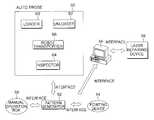
- FIG. 2is a block diagram showing a configuration of a conventional apparatus of inspecting cell badness in a liquid crystal display device according to an embodiment of the present invention.
- the inspecting apparatusincludes an auto probe 50 for loading a LCD panel to be inspected and then inspecting the same, a pattern generator 52 for applying a test pattern signal to the LCD panel loaded on the auto probe 50 , a pointing device 54 for rapidly acquiring co-ordinate values of a position at which a bad pixel is found in the inspecting process, a file server 56 for storing the co-ordinate values of bad pixels acquired at the pointing device 54 , and a laser repair device 58 for repairing the bad pixel of the LCD panel using a laser beam with the aid of the co-ordinate value of bad pixels applied automatically from the file server 56 .
- the auto probe 50includes a loader 60 for carrying a LCD panel to be inspected from the exterior thereof into the interior thereof, an unloader 62 for carrying an inspection-completed LCD from the auto probe 50 into the exterior thereof, an inspector 64 for making an inspecting work for the loaded LCD panel, and a robot transporter 66 for carrying the LCD panel put on the loader 60 into the inspector 64 or carrying the LCD panel positioned at the inspector 64 into the unloader 62 after completion of the inspection.
- the pattern generator 52is interfaced with the inspector 64 of the auto probe 50 to apply a test pattern signal to the inspector 64 .
- the pattern generator 52is interfaced with the pointing device 54 by means of a RS-232 port and the like to control an application of the test pattern signal by means of an operation button of the pointing device 54 .
- the pointing device 54is a device capable of freely operating a position of a cursor emerging on a screen of a LCD panel.
- the pointing device 54is a mouse mounted in a general personal computer, which is a device of permitting a worker to rapidly move a cursor emerging on a screen of a LCD panel upon inspection of the LCD panel using the pointing device 54 in all the direction.
- the file server 56is a personal computer for server, which is interfaced with the pointing device 54 interfacing the pattern generator 52 .
- Co-ordinate values of a bad pixel in a LCD panel acquired by the pointing device 54are automatically transmitted to be stored in the file server 56 as a data.
- the laser-repairing device 58is interfaced with the file server 56 to automatically transmit the data stored in the file server 56 to the laser-repairing device 58 after completing an inspection for the LCD panel, thereby performing an automatic repair work.
- a LCD panel to be inspected at the loader 60 of the auto probe 50is carried from the exterior into the interior of the auto probe 50 .
- the LCD panel carried into the loader 60is sent to the inspector 64 by means of the robot transporter 66 .
- the pattern generator 52When the LCD panel is safely loaded on the inspector 64 of the auto probe 50 , the pattern generator 52 generates a test pattern signal in response to a control signal applied from the pointing device 54 to apply the test pattern signal to the inspector 64 of the auto probe 50 .
- a test patternis expressed on a screen of the LCD panel loaded on the inspector 64 of the auto probe 50 .
- a workerobserves this screen to inspect whether or not a bad pixel exists.
- a worker's eyesenses pixel badness such as a poor color, a bright point, a dark point and a line defect, etc.
- a cursor moved by an operation of the pointing device 54is emerged on the screen of the LCD panel, and X-Y co-ordinates of the cursor are displayed at the edge portion of the screen.
- the workergrasps a position of the bad pixel and then operates the pointing device 54 to move a position of the cursor into the position of the bad pixel.
- the pointing device 54is a mouse connected to the pattern generator 52 by a user interface, which permits a worker to freely move a position of the cursor.
- the pointing device 54permits a movement of the cursor in all the direction unlike the conventional manual operation box 24 capable of moving the cursor only in the up, down, left and right direction, so that a worker can rapidly move the cursor into a position of a bad pixel. Furthermore, an accurate co-ordinate acquisition work may be performed by virtue of a cursor operation button provided in a manual operation box 68 so as to make a fine position control of the cursor moved into a position of a bad pixel rapidly. When the cursor is moved into that position of the bad pixel by an operation of the pointing device 54 , X-Y co-ordinates of the bad pixel are displayed at the edge portion of the screen.
- the conventional inspecting apparatusSince the conventional inspecting apparatus must move the cursor into a position of the bad pixel pushing the cursor operation button of the manual operation box 24 hundreds of times, a co-ordinate acquisition work required about 1 to 2 minutes per LCD panel. Otherwise, the present inspecting apparatus moves the cursor using the mouse, so that it takes only 20 to 30 seconds per LCD panel in acquiring co-ordinate values of the bad pixel. Accordingly, a required inspection time is dramatically shortened to be expected to improve the productivity. Also, the co-ordinate value data is automatically stored in the file server 56 interfaced with the pointing device 54 without allowing a worker to write the co-ordinate values of the bad pixel on the work paper, so that work efficiency can be improved.
- the LCD panel loaded on the inspector 64is transported into the unloader 62 by means of the robot transporter 62 and then carried from the unloader 62 into the exterior of the auto probe 50 . Subsequently, a LCD panel being subject to the next inspection is carried to the loader 60 of the auto probe 50 .
- a LCD panel in which bad pixels have been found in the inspecting processis sent to the laser-repairing device 58 to perform a repairing work for the bad pixels.
- the laser-repairing device 58 interfaced with the file server 56automatically receives an ID number of the inspected LCD panel and a co-ordinate value data of the bad pixel from the file server 56 .
- the laser beam generatoris automatically moved into the corresponding co-ordinates of the LCD panel in accordance with the transmitted co-ordinate value data and emits a laser beam to the corresponding bad pixel, thereby performing a repair work of the liquid crystal cell.
- the repairing work for the liquid crystal cellemploys a method of shorting TFT's of the liquid crystal cell by a laser beam to make a bright point of the corresponding cell, or of opening the electrodes to make a dark point of the corresponding cell.
- co-ordinate values of the bad pixelare rapidly acquired by virtue of the pointing device 54 capable of freely moving the cursor emerging on the screen of the LCD panel.
- the acquired co-ordinate valueis automatically transmitted to and stored in the file server 56 interfaced with the pointing device 54 , and the stored data is transmitted to the laser repairing device 58 during the later repair work for the bad pixel to make an automatic repair work. Accordingly, a faster inspection than the prior art can be not only made, but also an efficiency of the inspection work can be improved.
- the co-ordinate value data of the bad pixelsis automatically transmitted to the laser repairing device 58 to make an automatic repair work rather than allowing a worker to perform a repair work seeing the data written on the work paper, so that an error generation in the repair work can be prevented to improve a yield of the repair work.
Landscapes
- Physics & Mathematics (AREA)
- Nonlinear Science (AREA)
- General Physics & Mathematics (AREA)
- Engineering & Computer Science (AREA)
- Chemical & Material Sciences (AREA)
- Crystallography & Structural Chemistry (AREA)
- Optics & Photonics (AREA)
- Computer Hardware Design (AREA)
- Theoretical Computer Science (AREA)
- Liquid Crystal (AREA)
- Testing Of Optical Devices Or Fibers (AREA)
Abstract
Description
Claims (13)
Applications Claiming Priority (2)
| Application Number | Priority Date | Filing Date | Title |
|---|---|---|---|
| KR1019990050238AKR100560397B1 (en) | 1999-11-12 | 1999-11-12 | Cell defect inspection apparatus and method of liquid crystal display device |
| KR99-50238 | 1999-11-12 |
Publications (1)
| Publication Number | Publication Date |
|---|---|
| US6529837B1true US6529837B1 (en) | 2003-03-04 |
Family
ID=19619812
Family Applications (1)
| Application Number | Title | Priority Date | Filing Date |
|---|---|---|---|
| US09/709,484Expired - LifetimeUS6529837B1 (en) | 1999-11-12 | 2000-11-13 | Apparatus and method for inspecting cell defect of liquid crystal display device |
Country Status (2)
| Country | Link |
|---|---|
| US (1) | US6529837B1 (en) |
| KR (1) | KR100560397B1 (en) |
Cited By (32)
| Publication number | Priority date | Publication date | Assignee | Title |
|---|---|---|---|---|
| US20020000983A1 (en)* | 2000-05-19 | 2002-01-03 | Lg. Philips Lcd Co., Ltd. | Method for examining quality of flat panel display device |
| CN100449362C (en)* | 2005-06-03 | 2009-01-07 | 飞而康公司 | Liquid crystal display panel detection device |
| US20120191562A1 (en)* | 2008-10-02 | 2012-07-26 | Eco Atm Incorporated | Kiosk For Recycling Electronic Devices |
| US20130255054A1 (en)* | 2012-03-30 | 2013-10-03 | Jui-Yu LIN | Method of manufacturing particle-based image display |
| US9881284B2 (en) | 2008-10-02 | 2018-01-30 | ecoATM, Inc. | Mini-kiosk for recycling electronic devices |
| US9885672B2 (en) | 2016-06-08 | 2018-02-06 | ecoATM, Inc. | Methods and systems for detecting screen covers on electronic devices |
| US9904911B2 (en) | 2008-10-02 | 2018-02-27 | ecoATM, Inc. | Secondary market and vending system for devices |
| US9911102B2 (en) | 2014-10-02 | 2018-03-06 | ecoATM, Inc. | Application for device evaluation and other processes associated with device recycling |
| US10032140B2 (en) | 2008-10-02 | 2018-07-24 | ecoATM, LLC. | Systems for recycling consumer electronic devices |
| US10127647B2 (en) | 2016-04-15 | 2018-11-13 | Ecoatm, Llc | Methods and systems for detecting cracks in electronic devices |
| US10269110B2 (en) | 2016-06-28 | 2019-04-23 | Ecoatm, Llc | Methods and systems for detecting cracks in illuminated electronic device screens |
| US10401411B2 (en) | 2014-09-29 | 2019-09-03 | Ecoatm, Llc | Maintaining sets of cable components used for wired analysis, charging, or other interaction with portable electronic devices |
| US10417615B2 (en) | 2014-10-31 | 2019-09-17 | Ecoatm, Llc | Systems and methods for recycling consumer electronic devices |
| US10445708B2 (en) | 2014-10-03 | 2019-10-15 | Ecoatm, Llc | System for electrically testing mobile devices at a consumer-operated kiosk, and associated devices and methods |
| US10475002B2 (en) | 2014-10-02 | 2019-11-12 | Ecoatm, Llc | Wireless-enabled kiosk for recycling consumer devices |
| US10572946B2 (en) | 2014-10-31 | 2020-02-25 | Ecoatm, Llc | Methods and systems for facilitating processes associated with insurance services and/or other services for electronic devices |
| US10825082B2 (en) | 2008-10-02 | 2020-11-03 | Ecoatm, Llc | Apparatus and method for recycling mobile phones |
| US10860990B2 (en) | 2014-11-06 | 2020-12-08 | Ecoatm, Llc | Methods and systems for evaluating and recycling electronic devices |
| WO2021056202A1 (en)* | 2019-09-24 | 2021-04-01 | 深圳市大疆创新科技有限公司 | Static bad pixel correction method, image processing chip and camera device |
| EP3806050A1 (en)* | 2010-03-19 | 2021-04-14 | ecoATM, LLC | Apparatus and method for recycling mobile phones |
| US11010841B2 (en) | 2008-10-02 | 2021-05-18 | Ecoatm, Llc | Kiosk for recycling electronic devices |
| US11080672B2 (en) | 2014-12-12 | 2021-08-03 | Ecoatm, Llc | Systems and methods for recycling consumer electronic devices |
| US11462868B2 (en) | 2019-02-12 | 2022-10-04 | Ecoatm, Llc | Connector carrier for electronic device kiosk |
| US11482067B2 (en) | 2019-02-12 | 2022-10-25 | Ecoatm, Llc | Kiosk for evaluating and purchasing used electronic devices |
| US11798250B2 (en) | 2019-02-18 | 2023-10-24 | Ecoatm, Llc | Neural network based physical condition evaluation of electronic devices, and associated systems and methods |
| US11922467B2 (en) | 2020-08-17 | 2024-03-05 | ecoATM, Inc. | Evaluating an electronic device using optical character recognition |
| US11989710B2 (en) | 2018-12-19 | 2024-05-21 | Ecoatm, Llc | Systems and methods for vending and/or purchasing mobile phones and other electronic devices |
| US12033454B2 (en) | 2020-08-17 | 2024-07-09 | Ecoatm, Llc | Kiosk for evaluating and purchasing used electronic devices |
| US12271929B2 (en) | 2020-08-17 | 2025-04-08 | Ecoatm Llc | Evaluating an electronic device using a wireless charger |
| US12322259B2 (en) | 2018-12-19 | 2025-06-03 | Ecoatm, Llc | Systems and methods for vending and/or purchasing mobile phones and other electronic devices |
| US12321965B2 (en) | 2020-08-25 | 2025-06-03 | Ecoatm, Llc | Evaluating and recycling electronic devices |
| US12380420B2 (en) | 2019-12-18 | 2025-08-05 | Ecoatm, Llc | Systems and methods for vending and/or purchasing mobile phones and other electronic devices |
Families Citing this family (4)
| Publication number | Priority date | Publication date | Assignee | Title |
|---|---|---|---|---|
| KR100880215B1 (en)* | 2002-06-14 | 2009-01-28 | 엘지디스플레이 주식회사 | Auto Probe Inspection Equipment |
| KR100800562B1 (en)* | 2006-08-31 | 2008-02-04 | 동일파텍주식회사 | Defect position detection device of glass substrate for LCD |
| KR100841902B1 (en)* | 2006-12-01 | 2008-07-02 | 오성엘에스티(주) | Liquid Crystal Display Panel Reinspection System and Liquid Crystal Display Panel Inspection Reinspection Method |
| CN105892109B (en)* | 2016-05-25 | 2023-06-20 | 江西合力泰科技有限公司 | Device and method for detecting defective point of liquid crystal glass PI (polyimide) |
Citations (2)
| Publication number | Priority date | Publication date | Assignee | Title |
|---|---|---|---|---|
| US5235272A (en)* | 1991-06-17 | 1993-08-10 | Photon Dynamics, Inc. | Method and apparatus for automatically inspecting and repairing an active matrix LCD panel |
| US5459594A (en)* | 1994-06-01 | 1995-10-17 | Mitsubishi Denki Kabushiki Kaisha | Apparatus for inspecting on-off states of a scattering-type liquid crystal display panel |
Family Cites Families (4)
| Publication number | Priority date | Publication date | Assignee | Title |
|---|---|---|---|---|
| JPH0659229A (en)* | 1992-08-12 | 1994-03-04 | Sharp Corp | Liquid crystal display panel inspecting device |
| JPH10185764A (en)* | 1996-12-27 | 1998-07-14 | Sony Corp | Inspection device for liquid crystal display |
| JPH116987A (en)* | 1997-04-21 | 1999-01-12 | Mitsubishi Electric Corp | Test signal generator for image display device and image display device using the same |
| JPH10325780A (en)* | 1997-05-23 | 1998-12-08 | Matsushita Electric Ind Co Ltd | Display screen inspection device |
- 1999
- 1999-11-12KRKR1019990050238Apatent/KR100560397B1/ennot_activeExpired - Fee Related
- 2000
- 2000-11-13USUS09/709,484patent/US6529837B1/ennot_activeExpired - Lifetime
Patent Citations (3)
| Publication number | Priority date | Publication date | Assignee | Title |
|---|---|---|---|---|
| US5235272A (en)* | 1991-06-17 | 1993-08-10 | Photon Dynamics, Inc. | Method and apparatus for automatically inspecting and repairing an active matrix LCD panel |
| US5459410A (en)* | 1991-06-17 | 1995-10-17 | Photon Dynamics, Inc. | Method and apparatus for automatically inspecting and repairing an active matrix LCD panel |
| US5459594A (en)* | 1994-06-01 | 1995-10-17 | Mitsubishi Denki Kabushiki Kaisha | Apparatus for inspecting on-off states of a scattering-type liquid crystal display panel |
Cited By (70)
| Publication number | Priority date | Publication date | Assignee | Title |
|---|---|---|---|---|
| US20020000983A1 (en)* | 2000-05-19 | 2002-01-03 | Lg. Philips Lcd Co., Ltd. | Method for examining quality of flat panel display device |
| US6778156B2 (en)* | 2000-05-19 | 2004-08-17 | Lg.Philips Lcd Co., Ltd. | Method for examining quality of flat panel display device |
| CN100449362C (en)* | 2005-06-03 | 2009-01-07 | 飞而康公司 | Liquid crystal display panel detection device |
| US11080662B2 (en) | 2008-10-02 | 2021-08-03 | Ecoatm, Llc | Secondary market and vending system for devices |
| US10055798B2 (en)* | 2008-10-02 | 2018-08-21 | Ecoatm, Llc | Kiosk for recycling electronic devices |
| US11010841B2 (en) | 2008-10-02 | 2021-05-18 | Ecoatm, Llc | Kiosk for recycling electronic devices |
| US10853873B2 (en) | 2008-10-02 | 2020-12-01 | Ecoatm, Llc | Kiosks for evaluating and purchasing used electronic devices and related technology |
| US10825082B2 (en) | 2008-10-02 | 2020-11-03 | Ecoatm, Llc | Apparatus and method for recycling mobile phones |
| US20120191562A1 (en)* | 2008-10-02 | 2012-07-26 | Eco Atm Incorporated | Kiosk For Recycling Electronic Devices |
| US11443289B2 (en) | 2008-10-02 | 2022-09-13 | Ecoatm, Llc | Secondary market and vending system for devices |
| US9818160B2 (en) | 2008-10-02 | 2017-11-14 | ecoATM, Inc. | Kiosk for recycling electronic devices |
| US9881284B2 (en) | 2008-10-02 | 2018-01-30 | ecoATM, Inc. | Mini-kiosk for recycling electronic devices |
| US12340425B2 (en) | 2008-10-02 | 2025-06-24 | Ecoatm, Llc | Kiosk for recycling electronic devices |
| US9904911B2 (en) | 2008-10-02 | 2018-02-27 | ecoATM, Inc. | Secondary market and vending system for devices |
| US12198108B2 (en) | 2008-10-02 | 2025-01-14 | Ecoatm, Llc | Secondary market and vending system for devices |
| US10032140B2 (en) | 2008-10-02 | 2018-07-24 | ecoATM, LLC. | Systems for recycling consumer electronic devices |
| US11526932B2 (en) | 2008-10-02 | 2022-12-13 | Ecoatm, Llc | Kiosks for evaluating and purchasing used electronic devices and related technology |
| US12182773B2 (en) | 2008-10-02 | 2024-12-31 | Ecoatm, Llc | Secondary market and vending system for devices |
| US10157427B2 (en) | 2008-10-02 | 2018-12-18 | Ecoatm, Llc | Kiosk for recycling electronic devices |
| US11935138B2 (en) | 2008-10-02 | 2024-03-19 | ecoATM, Inc. | Kiosk for recycling electronic devices |
| US11107046B2 (en) | 2008-10-02 | 2021-08-31 | Ecoatm, Llc | Secondary market and vending system for devices |
| US11907915B2 (en) | 2008-10-02 | 2024-02-20 | Ecoatm, Llc | Secondary market and vending system for devices |
| US11790328B2 (en) | 2008-10-02 | 2023-10-17 | Ecoatm, Llc | Secondary market and vending system for devices |
| EP3806050A1 (en)* | 2010-03-19 | 2021-04-14 | ecoATM, LLC | Apparatus and method for recycling mobile phones |
| US9322714B2 (en)* | 2012-03-30 | 2016-04-26 | Delta Electronics, Inc. | Method of manufacturing particle-based image display |
| US20130255054A1 (en)* | 2012-03-30 | 2013-10-03 | Jui-Yu LIN | Method of manufacturing particle-based image display |
| TWI505007B (en)* | 2012-03-30 | 2015-10-21 | Delta Electronics Inc | Method for manufacturing a particle-based image display having a plurality of imaging cells |
| US20150113784A1 (en)* | 2012-03-30 | 2015-04-30 | Delta Electronics, Inc. | Method of manufacturing particle-based image display |
| US8976349B2 (en)* | 2012-03-30 | 2015-03-10 | Delta Electronics, Inc. | Method of manufacturing particle-based image display |
| CN103365025A (en)* | 2012-03-30 | 2013-10-23 | 台达电子工业股份有限公司 | Manufacturing method of granular image display with multiple imaging grooves |
| US10401411B2 (en) | 2014-09-29 | 2019-09-03 | Ecoatm, Llc | Maintaining sets of cable components used for wired analysis, charging, or other interaction with portable electronic devices |
| US10475002B2 (en) | 2014-10-02 | 2019-11-12 | Ecoatm, Llc | Wireless-enabled kiosk for recycling consumer devices |
| US12217221B2 (en) | 2014-10-02 | 2025-02-04 | Ecoatm, Llc | Wireless-enabled kiosk for recycling consumer devices |
| US9911102B2 (en) | 2014-10-02 | 2018-03-06 | ecoATM, Inc. | Application for device evaluation and other processes associated with device recycling |
| US11790327B2 (en) | 2014-10-02 | 2023-10-17 | Ecoatm, Llc | Application for device evaluation and other processes associated with device recycling |
| US10496963B2 (en) | 2014-10-02 | 2019-12-03 | Ecoatm, Llc | Wireless-enabled kiosk for recycling consumer devices |
| US11126973B2 (en) | 2014-10-02 | 2021-09-21 | Ecoatm, Llc | Wireless-enabled kiosk for recycling consumer devices |
| US10438174B2 (en) | 2014-10-02 | 2019-10-08 | Ecoatm, Llc | Application for device evaluation and other processes associated with device recycling |
| US11734654B2 (en) | 2014-10-02 | 2023-08-22 | Ecoatm, Llc | Wireless-enabled kiosk for recycling consumer devices |
| US12373801B2 (en) | 2014-10-03 | 2025-07-29 | Ecoatm, Llc | System for electrically testing mobile devices at a consumer-operated kiosk, and associated devices and methods |
| US10445708B2 (en) | 2014-10-03 | 2019-10-15 | Ecoatm, Llc | System for electrically testing mobile devices at a consumer-operated kiosk, and associated devices and methods |
| US11232412B2 (en) | 2014-10-03 | 2022-01-25 | Ecoatm, Llc | System for electrically testing mobile devices at a consumer-operated kiosk, and associated devices and methods |
| US11989701B2 (en) | 2014-10-03 | 2024-05-21 | Ecoatm, Llc | System for electrically testing mobile devices at a consumer-operated kiosk, and associated devices and methods |
| US12205081B2 (en) | 2014-10-31 | 2025-01-21 | Ecoatm, Llc | Systems and methods for recycling consumer electronic devices |
| US11436570B2 (en) | 2014-10-31 | 2022-09-06 | Ecoatm, Llc | Systems and methods for recycling consumer electronic devices |
| US10417615B2 (en) | 2014-10-31 | 2019-09-17 | Ecoatm, Llc | Systems and methods for recycling consumer electronic devices |
| US10572946B2 (en) | 2014-10-31 | 2020-02-25 | Ecoatm, Llc | Methods and systems for facilitating processes associated with insurance services and/or other services for electronic devices |
| US10860990B2 (en) | 2014-11-06 | 2020-12-08 | Ecoatm, Llc | Methods and systems for evaluating and recycling electronic devices |
| US11315093B2 (en) | 2014-12-12 | 2022-04-26 | Ecoatm, Llc | Systems and methods for recycling consumer electronic devices |
| US11080672B2 (en) | 2014-12-12 | 2021-08-03 | Ecoatm, Llc | Systems and methods for recycling consumer electronic devices |
| US12008520B2 (en) | 2014-12-12 | 2024-06-11 | Ecoatm, Llc | Systems and methods for recycling consumer electronic devices |
| US10127647B2 (en) | 2016-04-15 | 2018-11-13 | Ecoatm, Llc | Methods and systems for detecting cracks in electronic devices |
| US9885672B2 (en) | 2016-06-08 | 2018-02-06 | ecoATM, Inc. | Methods and systems for detecting screen covers on electronic devices |
| US10269110B2 (en) | 2016-06-28 | 2019-04-23 | Ecoatm, Llc | Methods and systems for detecting cracks in illuminated electronic device screens |
| US10909673B2 (en) | 2016-06-28 | 2021-02-02 | Ecoatm, Llc | Methods and systems for detecting cracks in illuminated electronic device screens |
| US11803954B2 (en) | 2016-06-28 | 2023-10-31 | Ecoatm, Llc | Methods and systems for detecting cracks in illuminated electronic device screens |
| US12322259B2 (en) | 2018-12-19 | 2025-06-03 | Ecoatm, Llc | Systems and methods for vending and/or purchasing mobile phones and other electronic devices |
| US11989710B2 (en) | 2018-12-19 | 2024-05-21 | Ecoatm, Llc | Systems and methods for vending and/or purchasing mobile phones and other electronic devices |
| US11482067B2 (en) | 2019-02-12 | 2022-10-25 | Ecoatm, Llc | Kiosk for evaluating and purchasing used electronic devices |
| US11462868B2 (en) | 2019-02-12 | 2022-10-04 | Ecoatm, Llc | Connector carrier for electronic device kiosk |
| US12300059B2 (en) | 2019-02-12 | 2025-05-13 | Ecoatm, Llc | Kiosk for evaluating and purchasing used electronic devices |
| US11843206B2 (en) | 2019-02-12 | 2023-12-12 | Ecoatm, Llc | Connector carrier for electronic device kiosk |
| US11798250B2 (en) | 2019-02-18 | 2023-10-24 | Ecoatm, Llc | Neural network based physical condition evaluation of electronic devices, and associated systems and methods |
| US12223684B2 (en) | 2019-02-18 | 2025-02-11 | Ecoatm, Llc | Neural network based physical condition evaluation of electronic devices, and associated systems and methods |
| WO2021056202A1 (en)* | 2019-09-24 | 2021-04-01 | 深圳市大疆创新科技有限公司 | Static bad pixel correction method, image processing chip and camera device |
| US12380420B2 (en) | 2019-12-18 | 2025-08-05 | Ecoatm, Llc | Systems and methods for vending and/or purchasing mobile phones and other electronic devices |
| US11922467B2 (en) | 2020-08-17 | 2024-03-05 | ecoATM, Inc. | Evaluating an electronic device using optical character recognition |
| US12271929B2 (en) | 2020-08-17 | 2025-04-08 | Ecoatm Llc | Evaluating an electronic device using a wireless charger |
| US12033454B2 (en) | 2020-08-17 | 2024-07-09 | Ecoatm, Llc | Kiosk for evaluating and purchasing used electronic devices |
| US12321965B2 (en) | 2020-08-25 | 2025-06-03 | Ecoatm, Llc | Evaluating and recycling electronic devices |
Also Published As
| Publication number | Publication date |
|---|---|
| KR100560397B1 (en) | 2006-03-14 |
| KR20010046454A (en) | 2001-06-15 |
Similar Documents
| Publication | Publication Date | Title |
|---|---|---|
| US6529837B1 (en) | Apparatus and method for inspecting cell defect of liquid crystal display device | |
| JP4740405B2 (en) | Alignment method and program recording medium | |
| KR101051730B1 (en) | Board Inspection and Correction Device and Board Evaluation System | |
| US7800568B2 (en) | Apparatus and method for inspecting liquid crystal display | |
| JP2007334262A (en) | Defect detection method for TFT array substrate and defect detection apparatus for TFT array substrate | |
| US6466882B1 (en) | Integrated system for detecting and repairing semiconductor defects and a method for controlling the same | |
| US7157921B2 (en) | TFT array inspection apparatus | |
| CN115132620A (en) | Mass transfer method and apparatus | |
| US6014035A (en) | Test system and test method for liquid crystal display device | |
| KR100820752B1 (en) | Probe inspection device for flat panel display device and probe inspection method using same | |
| CN110428764B (en) | Display panel detection method | |
| JP2000082729A5 (en) | ||
| JP4748392B2 (en) | TFT array substrate inspection equipment | |
| US7702486B2 (en) | Apparatus and method for managing liquid crystal substrate | |
| KR20050000731A (en) | System and method for preventing over-detection of flexible printed circuit board in optical inspection system | |
| KR20140098482A (en) | System and method for testing image display device | |
| Yasuda et al. | High-resolution defect detection for flat panel display using proximity capacitance image sensor | |
| KR100683525B1 (en) | Inspection and repair device for liquid crystal display device | |
| KR20080109609A (en) | Flat Panel Display Array Inspection and Repair Common Units | |
| JP2006053097A (en) | Display panel inspection apparatus and display panel inspection method | |
| JP3375265B2 (en) | Defect repair method and defect repair device for light transmissive display panel | |
| KR101296644B1 (en) | Auto Probe Device For Inspecting Liquid Crystal Display Panel | |
| KR20090006456A (en) | LCD panel inspection device and inspection method | |
| JP2002365224A (en) | Method for inspecting resin coating at terminal section of liquid crystal display | |
| KR100825314B1 (en) | Inspection equipment of thin film transistor array |
Legal Events
| Date | Code | Title | Description |
|---|---|---|---|
| AS | Assignment | Owner name:LG. PHILIPS LCD CO., LTD., KOREA, REPUBLIC OF Free format text:ASSIGNMENT OF ASSIGNORS INTEREST;ASSIGNOR:KANG, DONG WOO;REEL/FRAME:011661/0546 Effective date:20010321 | |
| STCF | Information on status: patent grant | Free format text:PATENTED CASE | |
| FEPP | Fee payment procedure | Free format text:PAYER NUMBER DE-ASSIGNED (ORIGINAL EVENT CODE: RMPN); ENTITY STATUS OF PATENT OWNER: LARGE ENTITY Free format text:PAYOR NUMBER ASSIGNED (ORIGINAL EVENT CODE: ASPN); ENTITY STATUS OF PATENT OWNER: LARGE ENTITY | |
| FPAY | Fee payment | Year of fee payment:4 | |
| AS | Assignment | Owner name:LG DISPLAY CO., LTD., KOREA, REPUBLIC OF Free format text:CHANGE OF NAME;ASSIGNOR:LG. PHILIPS LCD CO., LTD.;REEL/FRAME:021773/0029 Effective date:20080304 Owner name:LG DISPLAY CO., LTD.,KOREA, REPUBLIC OF Free format text:CHANGE OF NAME;ASSIGNOR:LG. PHILIPS LCD CO., LTD.;REEL/FRAME:021773/0029 Effective date:20080304 | |
| FEPP | Fee payment procedure | Free format text:PAYOR NUMBER ASSIGNED (ORIGINAL EVENT CODE: ASPN); ENTITY STATUS OF PATENT OWNER: LARGE ENTITY | |
| FPAY | Fee payment | Year of fee payment:8 | |
| FPAY | Fee payment | Year of fee payment:12 |