US6528820B1 - Semiconductor device and method of fabricating same - Google Patents
Semiconductor device and method of fabricating sameDownload PDFInfo
- Publication number
- US6528820B1 US6528820B1US08/785,486US78548697AUS6528820B1US 6528820 B1US6528820 B1US 6528820B1US 78548697 AUS78548697 AUS 78548697AUS 6528820 B1US6528820 B1US 6528820B1
- Authority
- US
- United States
- Prior art keywords
- semiconductor film
- substrate
- film
- display device
- semiconductor
- Prior art date
- Legal status (The legal status is an assumption and is not a legal conclusion. Google has not performed a legal analysis and makes no representation as to the accuracy of the status listed.)
- Expired - Lifetime
Links
Images


Classifications
- H—ELECTRICITY
- H01—ELECTRIC ELEMENTS
- H01L—SEMICONDUCTOR DEVICES NOT COVERED BY CLASS H10
- H01L21/00—Processes or apparatus adapted for the manufacture or treatment of semiconductor or solid state devices or of parts thereof
- H01L21/02—Manufacture or treatment of semiconductor devices or of parts thereof
- H01L21/02104—Forming layers
- H01L21/02365—Forming inorganic semiconducting materials on a substrate
- H01L21/02656—Special treatments
- H01L21/02664—Aftertreatments
- H01L21/02667—Crystallisation or recrystallisation of non-monocrystalline semiconductor materials, e.g. regrowth
- H01L21/02672—Crystallisation or recrystallisation of non-monocrystalline semiconductor materials, e.g. regrowth using crystallisation enhancing elements
- H—ELECTRICITY
- H01—ELECTRIC ELEMENTS
- H01L—SEMICONDUCTOR DEVICES NOT COVERED BY CLASS H10
- H01L21/00—Processes or apparatus adapted for the manufacture or treatment of semiconductor or solid state devices or of parts thereof
- H01L21/02—Manufacture or treatment of semiconductor devices or of parts thereof
- H01L21/02104—Forming layers
- H01L21/02365—Forming inorganic semiconducting materials on a substrate
- H01L21/02367—Substrates
- H01L21/0237—Materials
- H01L21/0242—Crystalline insulating materials
- H—ELECTRICITY
- H01—ELECTRIC ELEMENTS
- H01L—SEMICONDUCTOR DEVICES NOT COVERED BY CLASS H10
- H01L21/00—Processes or apparatus adapted for the manufacture or treatment of semiconductor or solid state devices or of parts thereof
- H01L21/02—Manufacture or treatment of semiconductor devices or of parts thereof
- H01L21/02104—Forming layers
- H01L21/02365—Forming inorganic semiconducting materials on a substrate
- H01L21/02518—Deposited layers
- H01L21/02521—Materials
- H01L21/02524—Group 14 semiconducting materials
- H01L21/02532—Silicon, silicon germanium, germanium
- H—ELECTRICITY
- H01—ELECTRIC ELEMENTS
- H01L—SEMICONDUCTOR DEVICES NOT COVERED BY CLASS H10
- H01L21/00—Processes or apparatus adapted for the manufacture or treatment of semiconductor or solid state devices or of parts thereof
- H01L21/02—Manufacture or treatment of semiconductor devices or of parts thereof
- H01L21/02104—Forming layers
- H01L21/02365—Forming inorganic semiconducting materials on a substrate
- H01L21/02518—Deposited layers
- H01L21/02587—Structure
- H01L21/0259—Microstructure
- H01L21/02595—Microstructure polycrystalline
- H—ELECTRICITY
- H01—ELECTRIC ELEMENTS
- H01L—SEMICONDUCTOR DEVICES NOT COVERED BY CLASS H10
- H01L21/00—Processes or apparatus adapted for the manufacture or treatment of semiconductor or solid state devices or of parts thereof
- H01L21/02—Manufacture or treatment of semiconductor devices or of parts thereof
- H01L21/04—Manufacture or treatment of semiconductor devices or of parts thereof the devices having potential barriers, e.g. a PN junction, depletion layer or carrier concentration layer
- H01L21/18—Manufacture or treatment of semiconductor devices or of parts thereof the devices having potential barriers, e.g. a PN junction, depletion layer or carrier concentration layer the devices having semiconductor bodies comprising elements of Group IV of the Periodic Table or AIIIBV compounds with or without impurities, e.g. doping materials
- H01L21/28—Manufacture of electrodes on semiconductor bodies using processes or apparatus not provided for in groups H01L21/20 - H01L21/268
- H01L21/28008—Making conductor-insulator-semiconductor electrodes
- H01L21/28017—Making conductor-insulator-semiconductor electrodes the insulator being formed after the semiconductor body, the semiconductor being silicon
- H01L21/28158—Making the insulator
- H—ELECTRICITY
- H01—ELECTRIC ELEMENTS
- H01L—SEMICONDUCTOR DEVICES NOT COVERED BY CLASS H10
- H01L21/00—Processes or apparatus adapted for the manufacture or treatment of semiconductor or solid state devices or of parts thereof
- H01L21/02—Manufacture or treatment of semiconductor devices or of parts thereof
- H01L21/04—Manufacture or treatment of semiconductor devices or of parts thereof the devices having potential barriers, e.g. a PN junction, depletion layer or carrier concentration layer
- H01L21/18—Manufacture or treatment of semiconductor devices or of parts thereof the devices having potential barriers, e.g. a PN junction, depletion layer or carrier concentration layer the devices having semiconductor bodies comprising elements of Group IV of the Periodic Table or AIIIBV compounds with or without impurities, e.g. doping materials
- H01L21/30—Treatment of semiconductor bodies using processes or apparatus not provided for in groups H01L21/20 - H01L21/26
- H01L21/322—Treatment of semiconductor bodies using processes or apparatus not provided for in groups H01L21/20 - H01L21/26 to modify their internal properties, e.g. to produce internal imperfections
- H01L21/3221—Treatment of semiconductor bodies using processes or apparatus not provided for in groups H01L21/20 - H01L21/26 to modify their internal properties, e.g. to produce internal imperfections of silicon bodies, e.g. for gettering
- H01L21/3226—Treatment of semiconductor bodies using processes or apparatus not provided for in groups H01L21/20 - H01L21/26 to modify their internal properties, e.g. to produce internal imperfections of silicon bodies, e.g. for gettering of silicon on insulator
- H—ELECTRICITY
- H10—SEMICONDUCTOR DEVICES; ELECTRIC SOLID-STATE DEVICES NOT OTHERWISE PROVIDED FOR
- H10D—INORGANIC ELECTRIC SEMICONDUCTOR DEVICES
- H10D30/00—Field-effect transistors [FET]
- H10D30/01—Manufacture or treatment
- H10D30/021—Manufacture or treatment of FETs having insulated gates [IGFET]
- H10D30/031—Manufacture or treatment of FETs having insulated gates [IGFET] of thin-film transistors [TFT]
- H10D30/0312—Manufacture or treatment of FETs having insulated gates [IGFET] of thin-film transistors [TFT] characterised by the gate electrodes
- H10D30/0314—Manufacture or treatment of FETs having insulated gates [IGFET] of thin-film transistors [TFT] characterised by the gate electrodes of lateral top-gate TFTs comprising only a single gate
- H—ELECTRICITY
- H10—SEMICONDUCTOR DEVICES; ELECTRIC SOLID-STATE DEVICES NOT OTHERWISE PROVIDED FOR
- H10D—INORGANIC ELECTRIC SEMICONDUCTOR DEVICES
- H10D30/00—Field-effect transistors [FET]
- H10D30/01—Manufacture or treatment
- H10D30/021—Manufacture or treatment of FETs having insulated gates [IGFET]
- H10D30/031—Manufacture or treatment of FETs having insulated gates [IGFET] of thin-film transistors [TFT]
- H10D30/0312—Manufacture or treatment of FETs having insulated gates [IGFET] of thin-film transistors [TFT] characterised by the gate electrodes
- H10D30/0316—Manufacture or treatment of FETs having insulated gates [IGFET] of thin-film transistors [TFT] characterised by the gate electrodes of lateral bottom-gate TFTs comprising only a single gate
- H—ELECTRICITY
- H10—SEMICONDUCTOR DEVICES; ELECTRIC SOLID-STATE DEVICES NOT OTHERWISE PROVIDED FOR
- H10D—INORGANIC ELECTRIC SEMICONDUCTOR DEVICES
- H10D30/00—Field-effect transistors [FET]
- H10D30/01—Manufacture or treatment
- H10D30/021—Manufacture or treatment of FETs having insulated gates [IGFET]
- H10D30/031—Manufacture or treatment of FETs having insulated gates [IGFET] of thin-film transistors [TFT]
- H10D30/0321—Manufacture or treatment of FETs having insulated gates [IGFET] of thin-film transistors [TFT] comprising silicon, e.g. amorphous silicon or polysilicon
- H—ELECTRICITY
- H10—SEMICONDUCTOR DEVICES; ELECTRIC SOLID-STATE DEVICES NOT OTHERWISE PROVIDED FOR
- H10D—INORGANIC ELECTRIC SEMICONDUCTOR DEVICES
- H10D30/00—Field-effect transistors [FET]
- H10D30/60—Insulated-gate field-effect transistors [IGFET]
- H10D30/67—Thin-film transistors [TFT]
- H10D30/6704—Thin-film transistors [TFT] having supplementary regions or layers in the thin films or in the insulated bulk substrates for controlling properties of the device
- H10D30/6713—Thin-film transistors [TFT] having supplementary regions or layers in the thin films or in the insulated bulk substrates for controlling properties of the device characterised by the properties of the source or drain regions, e.g. compositions or sectional shapes
- H10D30/6715—Thin-film transistors [TFT] having supplementary regions or layers in the thin films or in the insulated bulk substrates for controlling properties of the device characterised by the properties of the source or drain regions, e.g. compositions or sectional shapes characterised by the doping profiles, e.g. having lightly-doped source or drain extensions
- H—ELECTRICITY
- H10—SEMICONDUCTOR DEVICES; ELECTRIC SOLID-STATE DEVICES NOT OTHERWISE PROVIDED FOR
- H10D—INORGANIC ELECTRIC SEMICONDUCTOR DEVICES
- H10D30/00—Field-effect transistors [FET]
- H10D30/60—Insulated-gate field-effect transistors [IGFET]
- H10D30/67—Thin-film transistors [TFT]
- H10D30/6729—Thin-film transistors [TFT] characterised by the electrodes
- H10D30/673—Thin-film transistors [TFT] characterised by the electrodes characterised by the shapes, relative sizes or dispositions of the gate electrodes
- H10D30/6731—Top-gate only TFTs
- H—ELECTRICITY
- H10—SEMICONDUCTOR DEVICES; ELECTRIC SOLID-STATE DEVICES NOT OTHERWISE PROVIDED FOR
- H10D—INORGANIC ELECTRIC SEMICONDUCTOR DEVICES
- H10D30/00—Field-effect transistors [FET]
- H10D30/60—Insulated-gate field-effect transistors [IGFET]
- H10D30/67—Thin-film transistors [TFT]
- H10D30/6729—Thin-film transistors [TFT] characterised by the electrodes
- H10D30/6737—Thin-film transistors [TFT] characterised by the electrodes characterised by the electrode materials
- H10D30/6739—Conductor-insulator-semiconductor electrodes
- H—ELECTRICITY
- H10—SEMICONDUCTOR DEVICES; ELECTRIC SOLID-STATE DEVICES NOT OTHERWISE PROVIDED FOR
- H10D—INORGANIC ELECTRIC SEMICONDUCTOR DEVICES
- H10D30/00—Field-effect transistors [FET]
- H10D30/60—Insulated-gate field-effect transistors [IGFET]
- H10D30/67—Thin-film transistors [TFT]
- H10D30/674—Thin-film transistors [TFT] characterised by the active materials
- H10D30/6741—Group IV materials, e.g. germanium or silicon carbide
- H10D30/6743—Silicon
- H10D30/6745—Polycrystalline or microcrystalline silicon
- H—ELECTRICITY
- H10—SEMICONDUCTOR DEVICES; ELECTRIC SOLID-STATE DEVICES NOT OTHERWISE PROVIDED FOR
- H10D—INORGANIC ELECTRIC SEMICONDUCTOR DEVICES
- H10D62/00—Semiconductor bodies, or regions thereof, of devices having potential barriers
- H10D62/40—Crystalline structures
- H—ELECTRICITY
- H10—SEMICONDUCTOR DEVICES; ELECTRIC SOLID-STATE DEVICES NOT OTHERWISE PROVIDED FOR
- H10D—INORGANIC ELECTRIC SEMICONDUCTOR DEVICES
- H10D86/00—Integrated devices formed in or on insulating or conducting substrates, e.g. formed in silicon-on-insulator [SOI] substrates or on stainless steel or glass substrates
- H10D86/01—Manufacture or treatment
- H10D86/021—Manufacture or treatment of multiple TFTs
- H10D86/0221—Manufacture or treatment of multiple TFTs comprising manufacture, treatment or patterning of TFT semiconductor bodies
- H10D86/0223—Manufacture or treatment of multiple TFTs comprising manufacture, treatment or patterning of TFT semiconductor bodies comprising crystallisation of amorphous, microcrystalline or polycrystalline semiconductor materials
- H10D86/0225—Manufacture or treatment of multiple TFTs comprising manufacture, treatment or patterning of TFT semiconductor bodies comprising crystallisation of amorphous, microcrystalline or polycrystalline semiconductor materials using crystallisation-promoting species, e.g. using a Ni catalyst
- H—ELECTRICITY
- H10—SEMICONDUCTOR DEVICES; ELECTRIC SOLID-STATE DEVICES NOT OTHERWISE PROVIDED FOR
- H10D—INORGANIC ELECTRIC SEMICONDUCTOR DEVICES
- H10D86/00—Integrated devices formed in or on insulating or conducting substrates, e.g. formed in silicon-on-insulator [SOI] substrates or on stainless steel or glass substrates
- H10D86/01—Manufacture or treatment
- H10D86/021—Manufacture or treatment of multiple TFTs
- H10D86/0251—Manufacture or treatment of multiple TFTs characterised by increasing the uniformity of device parameters
- H—ELECTRICITY
- H10—SEMICONDUCTOR DEVICES; ELECTRIC SOLID-STATE DEVICES NOT OTHERWISE PROVIDED FOR
- H10D—INORGANIC ELECTRIC SEMICONDUCTOR DEVICES
- H10D86/00—Integrated devices formed in or on insulating or conducting substrates, e.g. formed in silicon-on-insulator [SOI] substrates or on stainless steel or glass substrates
- H10D86/201—Integrated devices formed in or on insulating or conducting substrates, e.g. formed in silicon-on-insulator [SOI] substrates or on stainless steel or glass substrates the substrates comprising an insulating layer on a semiconductor body, e.g. SOI
- H—ELECTRICITY
- H10—SEMICONDUCTOR DEVICES; ELECTRIC SOLID-STATE DEVICES NOT OTHERWISE PROVIDED FOR
- H10D—INORGANIC ELECTRIC SEMICONDUCTOR DEVICES
- H10D86/00—Integrated devices formed in or on insulating or conducting substrates, e.g. formed in silicon-on-insulator [SOI] substrates or on stainless steel or glass substrates
- H10D86/40—Integrated devices formed in or on insulating or conducting substrates, e.g. formed in silicon-on-insulator [SOI] substrates or on stainless steel or glass substrates characterised by multiple TFTs
- H10D86/421—Integrated devices formed in or on insulating or conducting substrates, e.g. formed in silicon-on-insulator [SOI] substrates or on stainless steel or glass substrates characterised by multiple TFTs having a particular composition, shape or crystalline structure of the active layer
- H10D86/425—Integrated devices formed in or on insulating or conducting substrates, e.g. formed in silicon-on-insulator [SOI] substrates or on stainless steel or glass substrates characterised by multiple TFTs having a particular composition, shape or crystalline structure of the active layer having different crystal properties in different TFTs or within an individual TFT
- H—ELECTRICITY
- H10—SEMICONDUCTOR DEVICES; ELECTRIC SOLID-STATE DEVICES NOT OTHERWISE PROVIDED FOR
- H10D—INORGANIC ELECTRIC SEMICONDUCTOR DEVICES
- H10D86/00—Integrated devices formed in or on insulating or conducting substrates, e.g. formed in silicon-on-insulator [SOI] substrates or on stainless steel or glass substrates
- H10D86/40—Integrated devices formed in or on insulating or conducting substrates, e.g. formed in silicon-on-insulator [SOI] substrates or on stainless steel or glass substrates characterised by multiple TFTs
- H10D86/60—Integrated devices formed in or on insulating or conducting substrates, e.g. formed in silicon-on-insulator [SOI] substrates or on stainless steel or glass substrates characterised by multiple TFTs wherein the TFTs are in active matrices
- H—ELECTRICITY
- H01—ELECTRIC ELEMENTS
- H01L—SEMICONDUCTOR DEVICES NOT COVERED BY CLASS H10
- H01L21/00—Processes or apparatus adapted for the manufacture or treatment of semiconductor or solid state devices or of parts thereof
- H01L21/02—Manufacture or treatment of semiconductor devices or of parts thereof
- H01L21/02104—Forming layers
- H01L21/02365—Forming inorganic semiconducting materials on a substrate
- H01L21/02656—Special treatments
- H01L21/02664—Aftertreatments
- H01L21/02667—Crystallisation or recrystallisation of non-monocrystalline semiconductor materials, e.g. regrowth
- H01L21/02675—Crystallisation or recrystallisation of non-monocrystalline semiconductor materials, e.g. regrowth using laser beams
- H01L21/02686—Pulsed laser beam
Definitions
- the present inventionrelates to a thin-film semiconductor having crystallinity and also to a method of fabricating such a thin-film semiconductor. Furthermore, the invention relates to a semiconductor device utilizing such a thin-film semiconductor. In addition, the invention relates to a method of fabricating this semiconductor device.
- TFTsthin-film transistors
- TFTsare known as high-temperature polysilicon TFTs or low-temperature polysilicon TFTs.
- High-temperature polysilicon TFT fabricationis a technique utilizing a heat treatment conducted at relatively high-temperatures such as 800° C., 900° C., and more, in fabricating crystalline silicon films. It can be said that this technique has derived from IC fabrication processes making use of single-crystal silicon wafers.
- quartz substrates withstanding the above-described heating temperaturesare used as substrates on which high-temperature polysilicon TFTs are formed.
- low-temperature polysilicon TFTsare fabricated on cheaper glass substrates which are, of course, inferior in heat resistance to quartz substrates.
- High-temperature polysilicon TFT fabrication technologyis characterized in that it can integrate TFTs having uniform characteristics on a substrate at a high density.
- low-temperature polysilicon TFTscan make use of glass substrates which are cheap and can easily provide large areas.
- high-temperature polysilicon TFTsdo not differ greatly from low-temperature polysilicon TFTs in characteristics. The slight differences between them are that high-temperature polysilicon TFTs are superior in production yield and uniformity of characteristics across the substrate while low-temperature polysilicon TFTs are superior in productivity and production cost.
- these characteristicsmean that these TFTs can operate at speeds about two orders of magnitude higher than those of TFTs using amorphous silicon.
- the characteristics of the high-temperature polysilicon TFTsare much inferior to those of MOS transistors using single-crystal silicon wafers.
- the S values of MOS transistors employing single-crystal silicon wafersare on the order of 60 to 70 mV/dec.
- their operating frequenciesare 1-2 orders of magnitude higher than those of high- and low-temperature polysilicon TFTs.
- TFTsare used to integrate the active matrix circuit of an active matrix liquid crystal display and its peripheral driver circuit on the same substrate. That is, the active matrix circuit and peripheral driver circuit are fabricated from TFTs on the same substrate.
- the source driver circuit of the peripheral driver circuitis required to operate considerably above 10 MHz.
- a margin of only several megahertzis given to the operating speed.
- a conceivable forthcoming techniqueis to integrate oscillator circuits, D/A converters, A/D converters, and digital circuits for performing various kinds of image processing on the same substrate, in addition to the peripheral driver circuit including a shift register circuit and a buffer circuit.
- the invention disclosed hereinis intended to provide TFTs capable of building a circuit which can be operated at the above-described high speeds (generally, more than tens of megahertz).
- a semiconductor devicecomprises a plurality of TFTs formed on a substrate having an insulating surface.
- the active layer of the TFTsis formed by a crystalline silicon film.
- This crystalline silicon filmis formed by making use of crystals grown radially from a multiplicity of points.
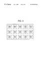
- This structureis obtained where the TFTs are fabricated, using the crystalline silicon film grown into morphologies shown in FIGS. 3 and 6.
- substrates having insulating surfacesinclude glass substrates (which are required to withstand the process temperature), quartz substrates, and semiconductor substrates having insulating films formed thereon.
- the above-described crystalline silicon film consisting of crystals grown radially from a multiplicity of pointscan be obtained by performing crystallization step, formation of a thermal oxide film, and removal of the thermal oxide film.
- the aforementioned crystallizationis carried out by a heat treatment, using a metallic element (typified by nickel as described later) that promotes crystallization of silicon.
- the thermal oxide film described aboveis formed in an oxidizing ambient containing a halogen element.
- Another semiconductor devicealso comprises a plurality of TFTs formed on a substrate having an insulating surface.
- the active layer of the TFTsis formed by a crystalline silicon film.
- This crystalline silicon filmis composed of a multiplicity of elongated crystalline structures grown in a certain direction. The widths of these crystalline structures range from dimensions comparable to the film thickness to 2000 ⁇ . The certain direction differs among the individual TFTs.
- the crystal growth direction(the direction of anisotropy of the elongated structures) in the active layer forming the TFTs differs among the individual TFTs.
- TFTshave active layers having the same crystal growth direction but most of the TFTs adopt the above-described structure.
- an active matrix circuitis made of a crystalline silicon film consisting of crystals grown into a morphology as shown in FIG. 3, numerous TFTs arranged in hundreds of devices x hundreds of devices achieve the above-described structure.
- the crystalline silicon film used in the present invention disclosed hereinconsists of crystals which are continuous with each other in a certain direction, as shown in FIG. 8 . These successive elongated crystal structures have widths ranging from dimensions comparable to the film thickness to about 2000 ⁇ . These numerous crystal structures form regions which extend substantially parallel on opposite sides of grain boundaries.
- a method according to the present inventioncomprises the steps of: forming an amorphous silicon film on an insulating surface; crystallizing the amorphous silicon film by the action of a metallic element that promotes crystallization of silicon to obtain a crystalline silicon film; performing thermal processing at 800-1100° C. in an oxidizing ambient containing a halogen element to form a first thermal oxide film on a surface of the crystalline silicon film; removing the first thermal oxide film; and forming a second thermal oxide film on the surface of the crystalline silicon film, whereby obtaining a final crystalline silicon film consisting of crystals grown radially from a multiplicity of points.
- Nickelis used quite advantageously as the metallic element for promoting crystallization of silicon in terms of reproducibility and effects.
- one or more elements selected from the group consisting of Fe, Co, Ni, Ru, Rh, Pd, Os, Ir, Pt, Cu, and Aucan be used as this metallic element.
- the concentration of nickel finally remaining in the silicon filmis approximately 1 ⁇ 10 14 to 5 ⁇ 10 18 atoms/cm 3 . If the gettering conditions for the thermal oxide films are optimized, the upper limit of this concentration can be reduced to about 5 ⁇ 10 17 atoms/cm 3 .
- the concentrationcan be measured by SIMS (secondary ion mass spectroscopy).
- the lower limit of the nickel concentrationis approximately 1 ⁇ 10 16 atoms/cm 3 . That is, this amount of nickel is left behind because it is normally difficult to remove the effects of nickel adhering to the substrate or equipment if the cost is also taken into account. However, the concentration of the residues can be reduced further by cleaning the equipment to a higher level or improving the manufacturing processes.
- the concentration of the remaining nickel elementis about 1 ⁇ 10 16 to 5 ⁇ 10 17 atoms/cm 3 .
- the metallic elementmoves into the thermal oxide film and so the concentration of nickel element in the direction of thickness of the obtained crystalline silicon film has a gradient or distribution.
- the concentration of the metallic element in the crystalline silicon filmtends to increase toward the interface at which the thermal oxide film is formed. Furthermore, it is observed that depending on the conditions, the concentration of the metallic element tends to increase toward the substrate or buffer layer, i.e., toward the interface on the back side.
- this halogen elementshows a concentration distribution similar to that of the metallic element. That is, the concentration distribution is such that the concentration increases toward the front surface and/or rear surface of the crystalline silicon film.
- the thickness of the final crystalline silicon film according to the present inventionis preferably set to 100 to 750 ⁇ , more preferably 150 to 450 ⁇ .
- the thickness of the final crystalline silicon filmbe determined by taking account of the fact that the film thickness is reduced by the deposition of the thermal oxide film.
- the crystalline silicon film described hereincan be obtained by adopting the manufacturing steps described above. Furthermore, MOS TFTs utilizing the special features of the crystalline structure can be obtained.
- Examples of the method of introducing the metallic elementinclude application of a solution containing this metallic element, a method using a CVD process, methods relying on sputtering or deposition, a plasma processing method using an electrode containing this metal, and a method making use of gas adsorption.
- a method of introducing a halogen elementcan use a means for adding HCl, HF, HBr, Cl 2 , F 2 , Br 2 , or CF 4 to an oxidizing ambient such as oxygen ambient.
- the temperature at which the thermal oxide film is grownis quite important. If one attempts to obtain a TFT which can be operated by itself at tens of megahertz or more and shows an S value of less than 100 mV/dec as described later, then it is necessary to set the heating temperature used during the formation of the thermal oxide film above 800° C., more preferably 900° C. or above.
- the upper limit of this heating temperatureshould be set to about 1100° C. which is the maximum processing temperature of quartz substrates.
- the present inventionlies in a technique for crystallizing an amorphous silicon film by means of heating to obtain a crystalline silicon film.
- This techniqueis characterized in that thermal processing is performed while holding nickel element in contact with the surface of the amorphous silicon film, thus giving rise to the crystalline silicon film.
- a thermal oxide filmis formed on the surface of this crystalline silicon film by performing thermal processing at 800-1100° C. in an oxidizing ambient containing a halogenic element.
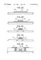
- FIGS. 1 (A)- 1 (D)are views illustrating a process sequence for fabricating a TFT
- FIGS. 2 (A)- 2 (E)are views illustrating a process sequence for fabricating a TFT
- FIG. 3is a diagram conceptually illustrating the state of grown crystals
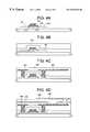
- FIGS. 4 (A)- 4 (D)are views illustrating a process sequence for fabricating a TFT
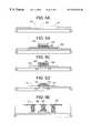
- FIGS. 5 (A)- 5 (E)are views illustrating a process sequence for fabricating a TFT
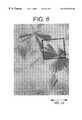
- FIG. 6is an electron micrograph of a thin silicon film
- FIG. 7is an electron micrograph of another thin silicon film
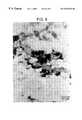
- FIG. 8is an electron micrograph of a further thin silicon film.
- FIGS. 9 (A)- 9 (F)are views schematically showing semiconductor devices according to the present invention.
- the present embodimentrelates to a method of obtaining a crystalline silicon film grown into a peculiar morphology as shown in FIG. 6, by introducing a metallic element for promoting crystallization of silicon into the whole surface of an amorphous silicon film.
- FIGS. 1 (A)- 1 (D)The process sequence of the present invention is shown in FIGS. 1 (A)- 1 (D).
- a silicon oxide filmis formed as a buffer layer 202 on a quartz substrate 201 to a thickness of 3000 ⁇ . If the surface of this quartz substrate has excellent flatness and is cleaned sufficiently, then this buffer layer 202 may be dispensed with.
- the material of the substrateis not limited to quartz as long as the substrate is capable of withstanding the heating temperature during the thermal processing.
- a semiconductor substrate having an oxide film deposited thereonmay also be used.
- an amorphous silicon film 203 acting as a starting film for a crystalline silicon filmis formed to a thickness of 500 ⁇ by LPCVD.
- nickel acetate solution containing 10 ppm (weight-converted value) of nickel elementis applied. Then, a spin-drying process is carried out, using a spinner (not shown), to remove a surplus of solution.
- a metallic elementfor promoting crystallization of silicon may be introduced by a method using a CVD process, sputtering, plasma processing, gas adsorption, or other method.
- This thermal processing for crystal growthcan be carried out at 450-1100° C.
- the upper limit of this temperature rangeis restricted by the heat resistance of the substrate. If some lateral growth distance should be secured, it is desired to set the heating temperature used in the heating processing to 600° C. or above. However, elevating the temperature further does not increase the crystal growth distance and crystallinity so much.
- laser light irradiationmay be performed. That is, the crystallization may be promoted further by laser light irradiation. This irradiation acts to disperse nickel element clusters existing in the film. This will facilitate removing the nickel element later. Even if laser light irradiation is effected at this stage, lateral growth will no longer proceed.
- the laser lightcan be emitted by an excimer laser having a wavelength lying in the UV range.
- an excimer laserhaving a wavelength lying in the UV range.
- a KrF excimer laserproducing a wavelength of 248 nm
- XeCl excimer laserproducing a wavelength of 308 nm
- a heat treatmentis done at 950° C. in an oxygen ambient containing 3% by volume of HCl. During this step, a thermal oxide film 209 is formed to a thickness of 200 ⁇ on the surface of the crystalline silicon film 205 (FIG. 1 (C)).
- the thickness of the crystalline silicon film 208decreases by about 100 ⁇ . That is, the thickness of the silicon film assumes a value of approximately 400 ⁇ .
- nickel elementis gettered out of the film because of the formation of the thermal oxide film and by the action of chlorine.
- FIG. 6is a photograph of an enlarged image obtained by an optical microscope.
- FIG. 7is an enlargement of a part of FIG. 6, and is a photograph take by a TEM (transmission electron microscope).
- FIG. 8is an enlargement of a part of FIG. 7, and is a photograph of an image observed with a TEM.
- FIG. 3pictorially shows the state of crystals grown over the whole film.
- the crystalline structuresextend in one direction which is coincident with the crystal growth direction, as shown in FIGS. 6 and 7. That is, a plurality of crystalline columns are arranged parallel on opposite sides of grain boundaries extending in one direction.
- These successive crystalline columnshave widths ranging from dimensions comparable to the film thickness to approximately 2000 ⁇ . Microscopically, they form regions extending substantially parallel on opposite sides of grain boundaries extending in a certain direction that is substantially coincident with the direction in which the above-described crystalline columns are continuous with each other.
- a patterning operationis carried out to create a pattern 302 consisting of laterally grown regions. These islands of region 302 will become an active layer for a TFT later.
- a silicon oxide film 304is formed to a thickness of 1000 ⁇ by plasma CVD. This silicon oxide film 304 will act as a gate-insulating film later.
- a heat treatmentis performed at 950° C. in an oxygen ambient containing 3% HCl to form a thermal oxide film 303 having a thickness of 300 ⁇ .
- This thermal oxide filmis formed on the surface of the pattern 302 becoming the active layer, as shown in FIG. 2 (A).
- the thickness of the pattern 302 becoming the active layerreaches 250 ⁇ .
- the thermal oxide film 303be thicker than the crystalline silicon film forming the active layer.
- the total thickness of the thermal oxide films 209 and 303be greater than the thickness of the finally obtained active layer.
- This thermal oxide film 211forms parts of the gate-insulating film. In this way, a state shown in FIG. 2 (A) is obtained.
- an aluminum film forming gate electrodesis formed to a thickness of 4000 ⁇ by sputtering.
- This aluminum filmcontains 0.2% by weight of scandium.
- the incorporation of the scandium in the aluminum filmis intended to suppress generation of hillocks and whiskers at later processing steps.
- the hillocks and whiskersare needle-like or prickle-like protrusions due to overgrowth of aluminum during heating.
- a dense anodic oxide film(not shown) is formed.
- an anodization processis carried out, using ethylene glycol solution containing 3% tartaric acid.
- the aluminum filmis used as an anode, and a cathode of platinum is also employed.
- the dense anodic oxide filmis formed to a thickness of 100 ⁇ on the aluminum film.
- This anodic oxide film(not shown) serves to improve the adhesion to a resist mask formed later.
- This anodic oxide filmcan be controlled by the voltage applied during the anodization.
- the resist maskindicated by 306 .
- the aluminum filmis patterned into stripes 305 , utilizing this resist mask. As a result, a state shown in FIG. 2 (B) is obtained.
- Anodizationis again effected.
- 3% aqueous solution of oxalic acidis used as an electrolytic solution.
- the anodizationis carried out, using the aluminum pattern 305 as an anode. Consequently, a porous anodic oxide film 308 is formed (FIG. 2 (C)).
- the anodic oxide film 308is formed selectively on the side surface of the aluminum pattern because the resist mask 306 adhering well exists thereon.
- This anodic oxide filmcan be grown to a thickness of several micrometers.
- the film thicknessis set to 6000 ⁇ .
- the growth distancecan be controlled by the anodization time.
- the electrolytic solutionintrudes into the porous anodic oxide film 308 and so a dense anodic oxide film 309 is formed.
- This dense anodic oxide film 309is set to 1000 ⁇ . This film thickness is controlled by the applied voltage.
- the exposed silicon oxide film 304is etched away.
- the thermal oxide film 303is etched by dry etching techniques.
- the remaining, CVD-grown silicon oxide filmis indicated by 310 .
- a thermal oxide film of the similar shapeis left behind under the left silicon oxide film.
- FIG. 2 (C)a state shown in FIG. 2 (C) is obtained.
- the porous anodic oxide film 308is removed, using mixed acid of acetic, nitric, and phosphoric acids. In this manner, a state shown in FIG. 2 (D) results.
- dopant ionsare implanted.
- phosphorus (P) ionsare introduced by plasma doping.
- heavily doped regions 311 , 315 and lightly doped regions 312 , 314are formed, because the remaining silicon oxide film 310 acts as a semi-transparent mask (a semi-blocking mask) and block some of the implanted ions.
- the source region 311 , a channel-forming region 313 , the drain region 315 , and lightly doped regions 312 , 314are formed by self-aligned technology.
- the region 314is a lightly doped drain (LDD) region (FIG. 2 (D)).
- LDDlightly doped drain
- the thickness of the dense anodic oxide film 309is increased to 2000 ⁇ or more, this great thickness permits formation of an offset gate region outside the channel-forming region 313 .
- an offset gate regionis formed but its dimensions are small. Hence, the contribution of the offset gate region is small and not shown for simplicity.
- the dense anodic oxide filmis made as thick as 2000 ⁇ or more, it is necessary to apply a voltage of more than 200 V. Hence, care must be taken to secure sufficient reproducibility and safety.
- a silicon nitride film 300is formed as an interlayer dielectric film by plasma CVD. Then, a polyimide resin film 316 is formed by spin coating.
- a contact holeis formed.
- a source electrode 317 and a drain electrode 318are formed. In this way, a TFT shown in FIG. 2 (E) is completed.
- the TFT of the present embodimentshows unparalleled characteristics.
- these S valuesare less than half of those of the conventional high-temperature and low-temperature polysilicon TFTs. That is, these are surprisingly excellent values.
- an operational amplifierUsing these TFTs, an operational amplifier, memory circuits, various kinds of arithmetic circuits and amplifiers can be formed on a quartz substrate.
- the present embodimentshows processing steps for fabricating the active matrix circuit portion of an active matrix liquid crystal display.
- FIGS. 4 (A)- 4 (D)The process sequence of the present embodiment is schematically shown in FIGS. 4 (A)- 4 (D).
- a crystalline silicon film and a liquid crystal displayare fabricated by the fabrication steps described in Embodiment 1.
- a state shown in FIG. 2 (D)(FIG. 4 (A)) is obtained by the fabrication steps shown in FIGS. 1 (A)- 1 (D) and 2 (A)- 2 (D).
- a silicon nitride film 401is formed as a first interlayer dielectric film to a thickness of 2000 ⁇ by plasma CVD. Then, a polyimide resin film 402 is spincoated. Thus, a state shown in FIG. 4 (B) is obtained.
- Polyamide and polyimideamidecan be used as resinous materials, as well as polyimide.
- a source electrode 403 and a drain electrode 403are created. These electrodes are fabricated from a Ti-Al-Ti lamination film. The source electrode 403 is formed so as to extend from a source line (FIG. 4 (C)).
- Portions of the drain electrode 403are employed as electrodes for forming an auxiliary capacitor.
- a polyimide resin film 404is formed as a second interlayer dielectric film.
- a state shown in FIG. 4 (C)is derived.
- a black matrix (BM) 405is fabricated from a lamination film of titanium and aluminum. Inherently, this black matrix 405 acts as a light-shielding film. Besides, this black matrix serves as electrodes forming auxiliary capacitors.
- a polyimide resin film 406is formed as a third interlayer dielectric film.
- a contact hole that permits access to the drain electrode 403is formed.
- a pixel electrode pattern 407is formed from ITO.
- the pattern of the black matrix 405overlaps the pattern of the pixel electrode 407 via the polyimide resin film 406 , thus forming the auxiliary capacitors.
- the present embodimentis similar to Embodiment 1 except that contacts are formed either on gate electrodes or on gate interconnects extending from the gate electrodes by a novel method.
- the side and top surfaces of the gate electrodesare coated with the dense anodic oxide film.
- this structureis very effective in suppressing hillocks and shorts between conductive interconnects.
- the present embodimentrelates to a structure for solving this problem.
- the process sequence of the present embodimentis shown in FIGS. 5 (A)- 5 (E). It is to be noted that like components, including details of fabrication conditions, are indicated by like reference numerals in various figures.
- an active layer pattern 210is formed from a crystalline silicon film.
- a lamination layer consisting of a thermal oxide film 211 and a CVD-grown oxide film 304is formed thereon.
- the CVD-grown oxide filmis first formed, followed by formation of the thermal oxide film.
- an aluminum filmis formed, and a silicon nitride film is formed to a thickness of 500 ⁇ .
- the laminateis patterned, using a resist mask 306 .
- an aluminum pattern 305 and an overlying silicon nitride film pattern 501are formed (FIG. 5 (B)).
- a porous anodic oxide film 308is formed while leaving the resist mask 306 behind.
- a denser anodic oxide film 309is formed.
- These anodic oxide filmsare formed selectively only on the side surfaces of the aluminum pattern 307 becoming gate electrodes, because the top surface of the aluminum pattern is capped with the silicon nitride film 501 .
- the resist mask 306is removed.
- the exposed silicon oxide film 304is also removed.
- the thermal oxide film 211is partially removed.
- a source region 311 , lightly doped regions 312 , 314 , a channel region 313 , and a drain region 315are formed by self-aligned technology.
- laser light irradiationis performed to anneal out the damage caused by the doping and to active the introduced dopant.
- FIG. 5 (D)arises.
- an interlayer dielectric film 502is formed.
- a contact holeis formed.
- a source electrode 317 , an electrode 503 extending from the gate, and a drain electrode 318are formed.
- a state shown in FIG. 5 (E)is obtained.
- the formation of the contact hole extending to the gate electrode 307can be performed relatively easily because no anodic oxide film resides on top of the gate electrode.
- Source/drain electrodes and gate electrodeare shown to be formed on the same cross section but, in practice, the electrode 503 is formed on a part of the gate electrode 307 extending from the gate electrode 307 .
- the present embodimentis an improvement over the configuration of Embodiment 3.
- a titanium filmis grown on the aluminum film forming the gate electrode.
- a silicon nitride filmis formed on the titanium film.
- the film 501is made of a lamination film of titanium and silicon nitride. This can suppress generation of hillocks on the top surface of the aluminum electrode in later processing steps.
- the present embodimentis similar to Embodiment 1 except that the substrate is made of glass.
- the substrateis made of Corning 1737 glass having a strain point of 667° C.
- a heat treatmentis made at 600° C. for 4 hours for crystallization.
- a heat treatment for formation of a thermal oxide filmis carried out at 640° C. in an oxygen ambient containing 3% by volume of HCl.
- the thickness of the thermal oxide film formedreaches about 30 ⁇ if the processing time is 2 hours.
- the resulting effectis smaller compared with the case where a heat treatment at 950° C. is added as in Embodiment 1.
- the present embodimentis similar to Embodiment 1 except that the ambient in which the thermal oxide film is formed does not contain HCl. In this case, the gettering effect of nickel is smaller than in the case where the ambient contains HCl.
- the present embodimentis similar to Embodiment 1 except that laser light irradiation is carried out after the formation of the thermal oxide film. This can promote the crystallization further.
- FIGS. 9 (A)- 9 (F)show examples of semiconductor device making use of TFTs. These various examples of semiconductor device are shown in FIGS. 9 (A)- 9 (F).
- FIG. 9 (A)there is shown a portable intelligent terminal whose body is indicated by 2001 .
- the bodycomprises an active matrix liquid crystal display 2005 including a memory. Required information can be read from the internal memory and displayed on the display 2005 . Furthermore, information accessed through a telephone line can be displayed on the display 2005 .
- the display deviceis an active matrix electroluminescent device.
- Various information-processing circuits and storage circuitsare fabricated as an integrated circuit 2006 , using TFTs, on the same substrate as the active matrix circuit forming the display device.
- the body 2001is equipped with a camera portion 2002 .
- Required image informationcan be picked up by operating an operation switch 2004 .
- the image picked up by the camera portion 2002is accepted into the instrument through an image-receiving portion 2003 .
- FIG. 9 (B)there is shown a head mounted display whose body is indicated by 2101 .
- This display unithas two active matrix liquid crystal displays 2102 which act to display images in a location several centimeters away from the user's eyes. This instrument permits virtual reality visualization.
- FIG. 9 (C)there is shown a car navigational system.
- This systemacts to measure positions, using signals from an artificial satellite, the signals being received by an antenna 2204 .
- the measured positionsare displayed on an active matrix liquid crystal display 2202 .
- the displayed informationis selected with an operation switch 2203 .
- an active matrix electroluminescent displaycan be utilized.
- FIG. 9 (D)An example of mobile telephone is shown in FIG. 9 (D).
- the body of this apparatusis indicated by 2301 and equipped with an antenna 2306 .
- the apparatushas a speech input portion 2303 and a speech output portion 2302 .
- operation switches 2305are operated.
- Various kinds of image informationare displayed on a display unit 2304 .
- an active matrix liquid crystal display or active matrix electroluminescent displayis employed.
- FIG. 9 (E)Shown in FIG. 9 (E) is a portable video camera whose body is indicated by 2401 .
- This apparatushas an image-receiving portion 2406 for picking up an image.
- This imageis stored in a magnetic tape loaded in the body 2401 .
- An integrated circuit 2407performs various kinds of digital processing on the image.
- This integrated circuit 2407may be a combination of conventional ICs chips or a combination of TFTs disclosed herein. Furthermore, these two types of devices may be combined.
- the image received by the image-receiving portion 2406 or stored in the internal magnetic tapeis displayed on the active matrix liquid crystal display 2402 .
- the apparatusis controlled with operation switches 2404 and powered by a battery 2405 .
- FIG. 9 (F)Shown in FIG. 9 (F) is a projection display system whose body is indicated by 2501 . An image projected by the body 2501 is displayed on a screen.
- the body 2501comprises a light source 2502 , an active matrix liquid crystal display 2503 for optically modulating the light from the light source and forming an image, and optics 2504 for projecting the image.
- the liquid crystal displaycan be either transmission type or reflection type.
- an actual circuitis designed to operate at about 10% of the oscillation frequency of the ring oscillator. Where this fact is taken into account, it can be said that a circuit operating at frequencies of about 40 MHz can be fabricated from the above-described TFTs.
- TFTSthin-film transistors
- the peripheral driver circuitcan be integrated with the active matrix circuit on the same substrate.
- a circuit which is required to exhibit various high-speed operationscan be fabricated as an integrated circuit from TFTs on the same substrate by utilizing the invention disclosed herein. Furthermore, a method of fabricating this circuit is provided.
Landscapes
- Engineering & Computer Science (AREA)
- Physics & Mathematics (AREA)
- Microelectronics & Electronic Packaging (AREA)
- General Physics & Mathematics (AREA)
- Manufacturing & Machinery (AREA)
- Computer Hardware Design (AREA)
- Condensed Matter Physics & Semiconductors (AREA)
- Power Engineering (AREA)
- Chemical & Material Sciences (AREA)
- Crystallography & Structural Chemistry (AREA)
- Optics & Photonics (AREA)
- Materials Engineering (AREA)
- Thin Film Transistor (AREA)
- Recrystallisation Techniques (AREA)
Abstract
Description
1. Field of the Invention
The present invention relates to a thin-film semiconductor having crystallinity and also to a method of fabricating such a thin-film semiconductor. Furthermore, the invention relates to a semiconductor device utilizing such a thin-film semiconductor. In addition, the invention relates to a method of fabricating this semiconductor device.
2. Description of the Related Art
Techniques for forming a crystalline silicon film on a glass substrate or quartz substrate and fabricating thin-film transistors (TFTs) from this silicon film are known.
These TFTs are known as high-temperature polysilicon TFTs or low-temperature polysilicon TFTs.
High-temperature polysilicon TFT fabrication is a technique utilizing a heat treatment conducted at relatively high-temperatures such as 800° C., 900° C., and more, in fabricating crystalline silicon films. It can be said that this technique has derived from IC fabrication processes making use of single-crystal silicon wafers.
Of course, quartz substrates withstanding the above-described heating temperatures are used as substrates on which high-temperature polysilicon TFTs are formed.
On the other hand, low-temperature polysilicon TFTs are fabricated on cheaper glass substrates which are, of course, inferior in heat resistance to quartz substrates.
When a crystalline silicon film forming low-temperature polysilicon TFTs is fabricated, a heat treatment at a temperature lower than 600° C. is used so that the glass substrate can stand up to it, or laser annealing technique which hardly thermally damages the glass substrate is exploited.
High-temperature polysilicon TFT fabrication technology is characterized in that it can integrate TFTs having uniform characteristics on a substrate at a high density.
On the other hand, low-temperature polysilicon TFTs can make use of glass substrates which are cheap and can easily provide large areas.
It is to be noted that with the current technology, high-temperature polysilicon TFTs do not differ greatly from low-temperature polysilicon TFTs in characteristics. The slight differences between them are that high-temperature polysilicon TFTs are superior in production yield and uniformity of characteristics across the substrate while low-temperature polysilicon TFTs are superior in productivity and production cost.
With respect to the characteristics, both kinds of TFTs show mobilities of approximately 50 to 100 cm2/ V s and S values of about 200 to 400 mV/dec (VD=1 V).
These characteristics mean that these TFTs can operate at speeds about two orders of magnitude higher than those of TFTs using amorphous silicon. However, the characteristics of the high-temperature polysilicon TFTs are much inferior to those of MOS transistors using single-crystal silicon wafers. Generally, the S values of MOS transistors employing single-crystal silicon wafers are on the order of 60 to 70 mV/dec. Furthermore, their operating frequencies are 1-2 orders of magnitude higher than those of high- and low-temperature polysilicon TFTs.
At present, TFTs are used to integrate the active matrix circuit of an active matrix liquid crystal display and its peripheral driver circuit on the same substrate. That is, the active matrix circuit and peripheral driver circuit are fabricated from TFTs on the same substrate.
In this configuration, the source driver circuit of the peripheral driver circuit is required to operate considerably above 10 MHz. Today, however, with respect to a circuit composed of high- and low-temperature polysilicon TFTs, a margin of only several megahertz is given to the operating speed.
Accordingly, it is customary to multiplex the operation, so that a matrix-driven liquid crystal display is fabricated. However, this method has the disadvantage that stripes appear on the viewing screen due to subtle deviations of timing of multiplexing.
A conceivable forthcoming technique is to integrate oscillator circuits, D/A converters, A/D converters, and digital circuits for performing various kinds of image processing on the same substrate, in addition to the peripheral driver circuit including a shift register circuit and a buffer circuit.
However, it is necessary that the aforementioned oscillator circuits, D/A converters, A/D converters, and digital circuits for performing various kinds of image processing operate at higher frequencies than the peripheral driver circuit.
Therefore, it is substantially impossible to fabricate these circuits from the high- and low-temperature polysilicon TFTs obtained by the current techniques.
It is to be noted that an integrated circuit which consists of MOS transistors using a single-crystal silicon wafer and can be operated above 100 MHz has been put into practical use.
The invention disclosed herein is intended to provide TFTs capable of building a circuit which can be operated at the above-described high speeds (generally, more than tens of megahertz).
It is another object of the invention to provide TFTs having characteristics comparable to those of MOS transistors fabricated, using a single-crystal silicon wafer. It is a further object of the invention to provide means for fabricating these TFTs. It is a yet other object of the invention to provide a semiconductor device to which requisite functions are imparted by TFTs having such excellent characteristics.
A semiconductor device according to the present invention comprises a plurality of TFTs formed on a substrate having an insulating surface. The active layer of the TFTs is formed by a crystalline silicon film. This crystalline silicon film is formed by making use of crystals grown radially from a multiplicity of points.
This structure is obtained where the TFTs are fabricated, using the crystalline silicon film grown into morphologies shown in FIGS. 3 and 6.
Examples of substrates having insulating surfaces include glass substrates (which are required to withstand the process temperature), quartz substrates, and semiconductor substrates having insulating films formed thereon.
The above-described crystalline silicon film consisting of crystals grown radially from a multiplicity of points can be obtained by performing crystallization step, formation of a thermal oxide film, and removal of the thermal oxide film. The aforementioned crystallization is carried out by a heat treatment, using a metallic element (typified by nickel as described later) that promotes crystallization of silicon. The thermal oxide film described above is formed in an oxidizing ambient containing a halogen element.
Another semiconductor device according to the invention also comprises a plurality of TFTs formed on a substrate having an insulating surface. The active layer of the TFTs is formed by a crystalline silicon film. This crystalline silicon film is composed of a multiplicity of elongated crystalline structures grown in a certain direction. The widths of these crystalline structures range from dimensions comparable to the film thickness to 2000 Å. The certain direction differs among the individual TFTs.
More specifically, where a number of TFTs are manufactured, using the crystalline silicon film grown into the crystal morphologies shown in FIGS. 3 and 6, the crystal growth direction (the direction of anisotropy of the elongated structures) in the active layer forming the TFTs differs among the individual TFTs.
Of course, some TFTs have active layers having the same crystal growth direction but most of the TFTs adopt the above-described structure.
For example, if an active matrix circuit is made of a crystalline silicon film consisting of crystals grown into a morphology as shown in FIG. 3, numerous TFTs arranged in hundreds of devices x hundreds of devices achieve the above-described structure.
The crystalline silicon film used in the present invention disclosed herein consists of crystals which are continuous with each other in a certain direction, as shown in FIG.8. These successive elongated crystal structures have widths ranging from dimensions comparable to the film thickness to about 2000 Å. These numerous crystal structures form regions which extend substantially parallel on opposite sides of grain boundaries.
Macroscopically, these crystal structures extend radially as shown in FIGS. 7 and 6.
A method according to the present invention comprises the steps of: forming an amorphous silicon film on an insulating surface; crystallizing the amorphous silicon film by the action of a metallic element that promotes crystallization of silicon to obtain a crystalline silicon film; performing thermal processing at 800-1100° C. in an oxidizing ambient containing a halogen element to form a first thermal oxide film on a surface of the crystalline silicon film; removing the first thermal oxide film; and forming a second thermal oxide film on the surface of the crystalline silicon film, whereby obtaining a final crystalline silicon film consisting of crystals grown radially from a multiplicity of points.
In the above-described method, in order to improve the quality of the final crystalline silicon film, it is important to make the total thickness of the first and second thermal oxide films greater than the thickness of the final crystalline silicon film.
This is because the formed thermal oxide films drastically improve the quality of the crystalline silicon film.
Nickel is used quite advantageously as the metallic element for promoting crystallization of silicon in terms of reproducibility and effects. Generally, one or more elements selected from the group consisting of Fe, Co, Ni, Ru, Rh, Pd, Os, Ir, Pt, Cu, and Au can be used as this metallic element.
Where nickel element is employed, the concentration of nickel finally remaining in the silicon film is approximately 1×10¹⁴to 5×10¹⁸atoms/cm3. If the gettering conditions for the thermal oxide films are optimized, the upper limit of this concentration can be reduced to about 5×10¹⁷atoms/cm3. The concentration can be measured by SIMS (secondary ion mass spectroscopy).
Generally, the lower limit of the nickel concentration is approximately 1×10¹⁶atoms/cm3. That is, this amount of nickel is left behind because it is normally difficult to remove the effects of nickel adhering to the substrate or equipment if the cost is also taken into account. However, the concentration of the residues can be reduced further by cleaning the equipment to a higher level or improving the manufacturing processes.
Accordingly, where general manufacturing processes are adopted, the concentration of the remaining nickel element is about 1×10¹⁶to 5×10¹⁷atoms/cm3.
During fabrication of a thermal oxide film, the metallic element moves into the thermal oxide film and so the concentration of nickel element in the direction of thickness of the obtained crystalline silicon film has a gradient or distribution.
Generally, it is observed that the concentration of the metallic element in the crystalline silicon film tends to increase toward the interface at which the thermal oxide film is formed. Furthermore, it is observed that depending on the conditions, the concentration of the metallic element tends to increase toward the substrate or buffer layer, i.e., toward the interface on the back side.
Where a halogen element is added to the ambient when a thermal oxide film is formed, this halogen element shows a concentration distribution similar to that of the metallic element. That is, the concentration distribution is such that the concentration increases toward the front surface and/or rear surface of the crystalline silicon film.
The thickness of the final crystalline silicon film according to the present invention is preferably set to 100 to 750 Å, more preferably 150 to 450 Å. By selecting the film thickness in this way, the crystalline structure shown in FIGS. 6-8 can be obtained more clearly and with improved reproducibility.
It is necessary that the thickness of the final crystalline silicon film be determined by taking account of the fact that the film thickness is reduced by the deposition of the thermal oxide film.
The crystalline silicon film described herein can be obtained by adopting the manufacturing steps described above. Furthermore, MOS TFTs utilizing the special features of the crystalline structure can be obtained.
Examples of the method of introducing the metallic element include application of a solution containing this metallic element, a method using a CVD process, methods relying on sputtering or deposition, a plasma processing method using an electrode containing this metal, and a method making use of gas adsorption.
A method of introducing a halogen element can use a means for adding HCl, HF, HBr, Cl2, F2, Br2, or CF4to an oxidizing ambient such as oxygen ambient.
Furthermore, when the thermal oxide film is fabricated, if hydrogen gas is also introduced into the ambient to make use of the action of wet oxidation, then desirable results arise.
The temperature at which the thermal oxide film is grown is quite important. If one attempts to obtain a TFT which can be operated by itself at tens of megahertz or more and shows an S value of less than 100 mV/dec as described later, then it is necessary to set the heating temperature used during the formation of the thermal oxide film above 800° C., more preferably 900° C. or above.
The upper limit of this heating temperature should be set to about 1100° C. which is the maximum processing temperature of quartz substrates.
The present invention lies in a technique for crystallizing an amorphous silicon film by means of heating to obtain a crystalline silicon film. This technique is characterized in that thermal processing is performed while holding nickel element in contact with the surface of the amorphous silicon film, thus giving rise to the crystalline silicon film. A thermal oxide film is formed on the surface of this crystalline silicon film by performing thermal processing at 800-1100° C. in an oxidizing ambient containing a halogenic element.
Thus, a crystalline silicon film grown into the peculiar crystalline state as shown in FIGS. 6-8 can be obtained.
FIGS.1(A)-1(D) are views illustrating a process sequence for fabricating a TFT;
FIGS.2(A)-2(E) are views illustrating a process sequence for fabricating a TFT;
FIG. 3 is a diagram conceptually illustrating the state of grown crystals;
FIGS.4(A)-4(D) are views illustrating a process sequence for fabricating a TFT;
FIGS.5(A)-5(E) are views illustrating a process sequence for fabricating a TFT;
FIG. 6 is an electron micrograph of a thin silicon film;
FIG. 7 is an electron micrograph of another thin silicon film;
FIG. 8 is an electron micrograph of a further thin silicon film; and
FIGS.9(A)-9(F) are views schematically showing semiconductor devices according to the present invention.
The present embodiment relates to a method of obtaining a crystalline silicon film grown into a peculiar morphology as shown in FIG. 6, by introducing a metallic element for promoting crystallization of silicon into the whole surface of an amorphous silicon film.
The process sequence of the present invention is shown in FIGS.1(A)-1(D). First, a silicon oxide film is formed as abuffer layer 202 on aquartz substrate 201 to a thickness of 3000 Å. If the surface of this quartz substrate has excellent flatness and is cleaned sufficiently, then thisbuffer layer 202 may be dispensed with.
At present, it is desired to use the quartz substrate. However, the material of the substrate is not limited to quartz as long as the substrate is capable of withstanding the heating temperature during the thermal processing. For instance, a semiconductor substrate having an oxide film deposited thereon may also be used.
Then, anamorphous silicon film 203 acting as a starting film for a crystalline silicon film is formed to a thickness of 500 Å by LPCVD.
Thereafter, nickel acetate solution containing 10 ppm (weight-converted value) of nickel element is applied. Then, a spin-drying process is carried out, using a spinner (not shown), to remove a surplus of solution.
In this way, nickel elements are present as shown by the dottedline 204 in FIG.1(A) to obtain a state shown in FIG.1(A).
Among methods of introducing nickel, the above-described method using the solution is excellent in controllability of the introduced amount and reproducibility. However, a metallic element (typified by nickel) for promoting crystallization of silicon may be introduced by a method using a CVD process, sputtering, plasma processing, gas adsorption, or other method.
Then, thermal processing is conducted at 600° C. for 8 hours in a nitrogen ambient which contains 3% hydrogen but contains a minimum amount of oxygen. As a result of this thermal processing, crystallization proceeds. Consequently, acrystalline silicon film 205 shown in FIG.1(B) is derived.
This thermal processing for crystal growth can be carried out at 450-1100° C. The upper limit of this temperature range is restricted by the heat resistance of the substrate. If some lateral growth distance should be secured, it is desired to set the heating temperature used in the heating processing to 600° C. or above. However, elevating the temperature further does not increase the crystal growth distance and crystallinity so much.
After the crystallization relying on this heating, laser light irradiation may be performed. That is, the crystallization may be promoted further by laser light irradiation. This irradiation acts to disperse nickel element clusters existing in the film. This will facilitate removing the nickel element later. Even if laser light irradiation is effected at this stage, lateral growth will no longer proceed.
The laser light can be emitted by an excimer laser having a wavelength lying in the UV range. For example, a KrF excimer laser (producing a wavelength of 248 nm) or XeCl excimer laser (producing a wavelength of 308 nm) can be exploited.
After the end of the thermal processing for the crystallization, a heat treatment is done at 950° C. in an oxygen ambient containing 3% by volume of HCl. During this step, athermal oxide film 209 is formed to a thickness of 200 Å on the surface of the crystalline silicon film205 (FIG.1(C)).
As a result of the formation of this thermal oxide film, the thickness of thecrystalline silicon film 208 decreases by about 100 Å. That is, the thickness of the silicon film assumes a value of approximately 400 Å.
During this step, as the thermal oxide film is formed, silicon element having unstable bonds in the film is used for the formation of the thermal oxide film. Defects in the film decrease, so that better crystallinity can be obtained.
At the same time, nickel element is gettered out of the film because of the formation of the thermal oxide film and by the action of chlorine.
Of course, a relatively high dose of nickel elements gets incorporated into thethermal oxide film 209 formed by this step. The relative concentration of nickel element within thesilicon film 208 decreases.
After the formation of thethermal oxide film 209, it is removed. In this way, thecrystalline silicon film 208 less doped with nickel element is obtained (FIG.1(D)).
In the crystalline silicon film obtained in this manner, crystals are grown radially from many local regions (many points) as shown in FIG. 6, which is a photograph of an enlarged image obtained by an optical microscope.
FIG. 7 is an enlargement of a part of FIG. 6, and is a photograph take by a TEM (transmission electron microscope).
In this crystalline structure, grain boundaries extend in the direction in which crystals are grown radially. Also, crystalline structures are continuous with each other in this direction. It is confirmed that the continuity of crystal lattices is substantially maintained in this direction.
FIG. 8 is an enlargement of a part of FIG. 7, and is a photograph of an image observed with a TEM. FIG. 3 pictorially shows the state of crystals grown over the whole film.
In this obtained crystalline silicon film, the crystalline structures extend in one direction which is coincident with the crystal growth direction, as shown in FIGS. 6 and 7. That is, a plurality of crystalline columns are arranged parallel on opposite sides of grain boundaries extending in one direction.
These successive crystalline columns have widths ranging from dimensions comparable to the film thickness to approximately 2000 Å. Microscopically, they form regions extending substantially parallel on opposite sides of grain boundaries extending in a certain direction that is substantially coincident with the direction in which the above-described crystalline columns are continuous with each other.
After thethermal oxide film 209 is removed and thecrystalline silicon film 208 as shown in FIG.1(D) is obtained, a patterning operation is carried out to create apattern 302 consisting of laterally grown regions. These islands ofregion 302 will become an active layer for a TFT later.
Then, as shown in FIG.2(A), after the formation of thepattern 302, asilicon oxide film 304 is formed to a thickness of 1000 Å by plasma CVD. Thissilicon oxide film 304 will act as a gate-insulating film later.
After forming thesilicon oxide film 304, a heat treatment is performed at 950° C. in an oxygen ambient containing 3% HCl to form athermal oxide film 303 having a thickness of 300 Å. This thermal oxide film is formed on the surface of thepattern 302 becoming the active layer, as shown in FIG.2(A).
As a result of thethermal oxide film 211, the thickness of thepattern 302 becoming the active layer reaches 250 Å.
If a TFT of higher performance should be obtained, it is desired that thethermal oxide film 303 be thicker than the crystalline silicon film forming the active layer.
In general, it is important that the total thickness of thethermal oxide films
Thisthermal oxide film 211 forms parts of the gate-insulating film. In this way, a state shown in FIG.2(A) is obtained.
Then, an aluminum film forming gate electrodes is formed to a thickness of 4000 Å by sputtering. This aluminum film contains 0.2% by weight of scandium.
The incorporation of the scandium in the aluminum film is intended to suppress generation of hillocks and whiskers at later processing steps. The hillocks and whiskers are needle-like or prickle-like protrusions due to overgrowth of aluminum during heating.
After the formation of the aluminum film, a dense anodic oxide film (not shown) is formed. For this purpose, an anodization process is carried out, using ethylene glycol solution containing 3% tartaric acid. The aluminum film is used as an anode, and a cathode of platinum is also employed. In this step, the dense anodic oxide film is formed to a thickness of 100 Å on the aluminum film.
This anodic oxide film (not shown) serves to improve the adhesion to a resist mask formed later.
The thickness of this anodic oxide film can be controlled by the voltage applied during the anodization.
Then, the resist mask, indicated by306, is formed. The aluminum film is patterned intostripes 305, utilizing this resist mask. As a result, a state shown in FIG.2(B) is obtained.
Anodization is again effected. During this step, 3% aqueous solution of oxalic acid is used as an electrolytic solution. Within this electrolytic solution, the anodization is carried out, using thealuminum pattern 305 as an anode. Consequently, a porousanodic oxide film 308 is formed (FIG.2(C)).
In this step, theanodic oxide film 308 is formed selectively on the side surface of the aluminum pattern because the resistmask 306 adhering well exists thereon.
This anodic oxide film can be grown to a thickness of several micrometers. In this embodiment, the film thickness is set to 6000 Å. The growth distance can be controlled by the anodization time.
Then, the resistmask 306 is removed. Subsequently, another dense anodic oxide film is formed. In particular, anodization is again performed, using an electrolytic solution consisting of the aforementioned ethylene glycol solution containing 3% tartaric acid.
During this step, the electrolytic solution intrudes into the porousanodic oxide film 308 and so a denseanodic oxide film 309 is formed.
The thickness of this denseanodic oxide film 309 is set to 1000 Å. This film thickness is controlled by the applied voltage.
Then, the exposedsilicon oxide film 304 is etched away. At the same time, thethermal oxide film 303 is etched by dry etching techniques.
The remaining, CVD-grown silicon oxide film is indicated by310. A thermal oxide film of the similar shape is left behind under the left silicon oxide film.
In this way, a state shown in FIG.2(C) is obtained. The porousanodic oxide film 308 is removed, using mixed acid of acetic, nitric, and phosphoric acids. In this manner, a state shown in FIG.2(D) results.
After obtaining the state shown in FIG.2(D), dopant ions are implanted. In this embodiment, phosphorus (P) ions are introduced by plasma doping.
During this step, heavily dopedregions regions silicon oxide film 310 acts as a semi-transparent mask (a semi-blocking mask) and block some of the implanted ions.
Laser light or other intense light from a lamp is irradiated to activate the dopant ion-implanted regions. In this way, thesource region 311, a channel-formingregion 313, thedrain region 315, and lightly dopedregions
Theregion 314 is a lightly doped drain (LDD) region (FIG.2(D)).
Where the thickness of the denseanodic oxide film 309 is increased to 2000 Å or more, this great thickness permits formation of an offset gate region outside the channel-formingregion 313.
Also in the present invention, an offset gate region is formed but its dimensions are small. Hence, the contribution of the offset gate region is small and not shown for simplicity.
When the dense anodic oxide film is made as thick as 2000 Å or more, it is necessary to apply a voltage of more than 200 V. Hence, care must be taken to secure sufficient reproducibility and safety.
After obtaining the state shown in FIG.2(D), asilicon nitride film 300 is formed as an interlayer dielectric film by plasma CVD. Then, apolyimide resin film 316 is formed by spin coating.
Thereafter, a contact hole is formed. Asource electrode 317 and adrain electrode 318 are formed. In this way, a TFT shown in FIG.2(E) is completed.
The TFT of the present embodiment shows unparalleled characteristics.
For example, a high-performance NTFT (N-channel TFT) having a mobility of 200 to 300 cm2/ V s and an S value of 75 to 90 mV/dec (VD=1 V) is obtained. Furthermore, a high-performance PTFT (P-channel TFT) having a mobility of 120 to 180 cm2/ V s and an S value of 75 to 100 mV/dec (VD=1 V) is derived.
Especially, these S values are less than half of those of the conventional high-temperature and low-temperature polysilicon TFTs. That is, these are surprisingly excellent values.
Using these TFTs, an operational amplifier, memory circuits, various kinds of arithmetic circuits and amplifiers can be formed on a quartz substrate.
The present embodiment shows processing steps for fabricating the active matrix circuit portion of an active matrix liquid crystal display.
The process sequence of the present embodiment is schematically shown in FIGS.4(A)-4(D). A crystalline silicon film and a liquid crystal display are fabricated by the fabrication steps described in Embodiment 1. A state shown in FIG.2(D) (FIG.4(A)) is obtained by the fabrication steps shown in FIGS.1(A)-1(D) and2(A)-2(D).
After obtaining the state shown in FIG.4(A), asilicon nitride film 401 is formed as a first interlayer dielectric film to a thickness of 2000 Å by plasma CVD. Then, apolyimide resin film 402 is spincoated. Thus, a state shown in FIG.4(B) is obtained. Polyamide and polyimideamide can be used as resinous materials, as well as polyimide.
Then, contact holes extending to thesource region 311 and to thedrain region 315 are formed. Asource electrode 403 and adrain electrode 403 are created. These electrodes are fabricated from a Ti-Al-Ti lamination film. Thesource electrode 403 is formed so as to extend from a source line (FIG.4(C)).
Portions of thedrain electrode 403 are employed as electrodes for forming an auxiliary capacitor.
After forming the source and drain electrodes, apolyimide resin film 404 is formed as a second interlayer dielectric film. Thus, a state shown in FIG.4(C) is derived.
Then, a window is formed in the resinousinterlayer dielectric film 404. A black matrix (BM)405 is fabricated from a lamination film of titanium and aluminum. Inherently, thisblack matrix 405 acts as a light-shielding film. Besides, this black matrix serves as electrodes forming auxiliary capacitors.
After forming theblack matrix 405, apolyimide resin film 406 is formed as a third interlayer dielectric film. A contact hole that permits access to thedrain electrode 403 is formed. Apixel electrode pattern 407 is formed from ITO.
The pattern of theblack matrix 405 overlaps the pattern of thepixel electrode 407 via thepolyimide resin film 406, thus forming the auxiliary capacitors.
The present embodiment is similar to Embodiment 1 except that contacts are formed either on gate electrodes or on gate interconnects extending from the gate electrodes by a novel method.
In Embodiment 1, the side and top surfaces of the gate electrodes are coated with the dense anodic oxide film.
Where the electrodes are fabricated from aluminum, this structure is very effective in suppressing hillocks and shorts between conductive interconnects.
However, the densification of the film makes it relatively difficult to form contacts.
The present embodiment relates to a structure for solving this problem. The process sequence of the present embodiment is shown in FIGS.5(A)-5(E). It is to be noted that like components, including details of fabrication conditions, are indicated by like reference numerals in various figures.
First, as shown in FIG.5(A), anactive layer pattern 210 is formed from a crystalline silicon film. A lamination layer consisting of athermal oxide film 211 and a CVD-grownoxide film 304 is formed thereon.
In this embodiment, the CVD-grown oxide film is first formed, followed by formation of the thermal oxide film.
After obtaining the state shown in FIG.5(A), an aluminum film is formed, and a silicon nitride film is formed to a thickness of 500 Å. The laminate is patterned, using a resistmask 306. As a result, analuminum pattern 305 and an overlying siliconnitride film pattern 501 are formed (FIG.5(B)).
After obtaining the state shown in FIG.5(B), a porousanodic oxide film 308 is formed while leaving the resistmask 306 behind. A denseranodic oxide film 309 is formed.
These anodic oxide films are formed selectively only on the side surfaces of thealuminum pattern 307 becoming gate electrodes, because the top surface of the aluminum pattern is capped with thesilicon nitride film 501.
After the formation of the anodic oxide film, the resistmask 306 is removed. The exposedsilicon oxide film 304 is also removed. Thethermal oxide film 211 is partially removed.
In this way, a state shown in FIG.5(C) is obtained. Then, the resistmask 306 is removed, and the porousanodic oxide film 308 is removed.
Subsequently, thesilicon nitride film 501 is removed. This results in a state shown in FIG.5(D). Under this condition, a dopant that imparts a conductivity type is implanted by plasma doping.
As a result, asource region 311, lightly dopedregions channel region 313, and adrain region 315 are formed by self-aligned technology.
After the dopant doping, laser light irradiation is performed to anneal out the damage caused by the doping and to active the introduced dopant.
In this way, a state shown in FIG.5(D) arises. Then, aninterlayer dielectric film 502 is formed. A contact hole is formed. Asource electrode 317, anelectrode 503 extending from the gate, and adrain electrode 318 are formed. Thus, a state shown in FIG.5(E) is obtained.
During this step, the formation of the contact hole extending to thegate electrode 307 can be performed relatively easily because no anodic oxide film resides on top of the gate electrode.
Source/drain electrodes and gate electrode are shown to be formed on the same cross section but, in practice, theelectrode 503 is formed on a part of thegate electrode 307 extending from thegate electrode 307.
The present embodiment is an improvement over the configuration of Embodiment 3. In the present embodiment, a titanium film is grown on the aluminum film forming the gate electrode. A silicon nitride film is formed on the titanium film.
In particular, in a configuration shown in FIG.5(B), thefilm 501 is made of a lamination film of titanium and silicon nitride. This can suppress generation of hillocks on the top surface of the aluminum electrode in later processing steps.
The present embodiment is similar to Embodiment 1 except that the substrate is made of glass.
In the present embodiment, the substrate is made of Corning 1737 glass having a strain point of 667° C. A heat treatment is made at 600° C. for 4 hours for crystallization.
A heat treatment for formation of a thermal oxide film is carried out at 640° C. in an oxygen ambient containing 3% by volume of HCl. In this case, the thickness of the thermal oxide film formed reaches about 30 Å if the processing time is 2 hours. The resulting effect is smaller compared with the case where a heat treatment at 950° C. is added as in Embodiment 1.
The present embodiment is similar to Embodiment 1 except that the ambient in which the thermal oxide film is formed does not contain HCl. In this case, the gettering effect of nickel is smaller than in the case where the ambient contains HCl.
The present embodiment is similar to Embodiment 1 except that laser light irradiation is carried out after the formation of the thermal oxide film. This can promote the crystallization further.
The present embodiment shows examples of semiconductor device making use of TFTs. These various examples of semiconductor device are shown in FIGS.9(A)-9(F). Referring to FIG.9(A), there is shown a portable intelligent terminal whose body is indicated by2001. The body comprises an active matrixliquid crystal display 2005 including a memory. Required information can be read from the internal memory and displayed on thedisplay 2005. Furthermore, information accessed through a telephone line can be displayed on thedisplay 2005.
It can be considered that the display device is an active matrix electroluminescent device. Various information-processing circuits and storage circuits are fabricated as anintegrated circuit 2006, using TFTs, on the same substrate as the active matrix circuit forming the display device.
Thebody 2001 is equipped with acamera portion 2002. Required image information can be picked up by operating anoperation switch 2004. The image picked up by thecamera portion 2002 is accepted into the instrument through an image-receivingportion 2003.
Referring next to FIG.9(B), there is shown a head mounted display whose body is indicated by2101. A user puts on thisbody 2101. This display unit has two active matrixliquid crystal displays 2102 which act to display images in a location several centimeters away from the user's eyes. This instrument permits virtual reality visualization.
Referring next to FIG.9(C), there is shown a car navigational system. This system acts to measure positions, using signals from an artificial satellite, the signals being received by anantenna 2204. The measured positions are displayed on an active matrixliquid crystal display 2202. The displayed information is selected with anoperation switch 2203.
Instead of the liquid crystal display, an active matrix electroluminescent display can be utilized.
An example of mobile telephone is shown in FIG.9(D). The body of this apparatus is indicated by2301 and equipped with anantenna 2306. The apparatus has aspeech input portion 2303 and aspeech output portion 2302.
When the user telephones, operation switches2305 are operated. Various kinds of image information are displayed on adisplay unit 2304. To make the display unit portable, an active matrix liquid crystal display or active matrix electroluminescent display is employed.
Shown in FIG.9(E) is a portable video camera whose body is indicated by2401. This apparatus has an image-receivingportion 2406 for picking up an image. This image is stored in a magnetic tape loaded in thebody 2401.
Anintegrated circuit 2407 performs various kinds of digital processing on the image. Thisintegrated circuit 2407 may be a combination of conventional ICs chips or a combination of TFTs disclosed herein. Furthermore, these two types of devices may be combined.
The image received by the image-receivingportion 2406 or stored in the internal magnetic tape is displayed on the active matrixliquid crystal display 2402. The apparatus is controlled withoperation switches 2404 and powered by abattery 2405.
Shown in FIG.9(F) is a projection display system whose body is indicated by2501. An image projected by thebody 2501 is displayed on a screen.
Thebody 2501 comprises alight source 2502, an active matrixliquid crystal display 2503 for optically modulating the light from the light source and forming an image, andoptics 2504 for projecting the image.
Excluding the apparatus shown in FIG.9(B), the liquid crystal display can be either transmission type or reflection type.
Where a 9-stage ring oscillator is built by combining PTFTs and NTFTs obtained by making use of the invention disclosed herein, oscillations above 400 MHz are possible.
Generally, an actual circuit is designed to operate at about 10% of the oscillation frequency of the ring oscillator. Where this fact is taken into account, it can be said that a circuit operating at frequencies of about 40 MHz can be fabricated from the above-described TFTs.
In this way, thin-film transistors (TFTS) capable of forming a circuit which is required to operate at high speeds (generally, tens of megahertz or above) can be obtained by exploiting the invention disclosed herein.
Accordingly, for example, without operating the peripheral driver circuit of an active matrix liquid crystal display by a multiplexing scheme, the peripheral driver circuit can be integrated with the active matrix circuit on the same substrate.
With respect to S values, characteristics comparable to those of MOS transistors fabricated, using a single-crystal silicon wafer of less than 100 mV/dec, can be obtained.
A circuit which is required to exhibit various high-speed operations can be fabricated as an integrated circuit from TFTs on the same substrate by utilizing the invention disclosed herein. Furthermore, a method of fabricating this circuit is provided.
Claims (29)
1. An electroluminescence display device having a display portion, comprising:
a substrate having an insulating surface; and
a plurality of thin film transistors in said display portion over said substrate, each thin film transistor having an active layer formed by patterning a semiconductor film which has a thickness of 100 to 700 Å,
wherein said semiconductor film comprises a plurality of crystal grains of silicon through the whole area of the semiconductor film, each of said crystal grains growing radially from each of a plurality of points distributed through the whole surface of said semiconductor film, and
wherein crystal growth directions in said active layers differs from one of said plurality of thin film transistors to another, respectively.
2. A device according toclaim 1 wherein said semiconductor film comprises silicon.
3. A device according toclaim 1 wherein said electroluminescence display device is an active matrix type display device.
4. A device according toclaim 1 wherein said electroluminescence display device is included in an electro-optical device selected from the group consisting of a portable intelligent terminal, a car navigational system, and a mobile telephone.
5. An electroluminescence display device having a display portion comprising:
a substrate having an insulating surface; and
a plurality of thin film transistors in said display portion over said substrate, each thin film transistor having an active layer formed by patterning a semiconductor film which has a thickness of 100 to 700 Å,
wherein said semiconductor film comprises a plurality of crystal grains of silicon through the whole area of the semiconductor film, each of said crystal grains growing radially from each of a plurality of points distributed through the whole surface of said semiconductor film, and
wherein directions of anisotropy of crystal structures in active layers differs from one of said plurality of thin film transistors to another, respectively.
6. A device according toclaim 5 wherein said semiconductor device is an active matrix type display device.
7. A device according toclaim 5 wherein said electroluminescence display device is included in an electro-optical device selected from the group consisting of a portable intelligent terminal, a car navigational system, and a mobile telephone.
8. An electroluminescence display device having a display portion, comprising:
a substrate having an insulating surface; and
a plurality of thin film transistors in said display portion over said substrate, each thin film transistor having:
an active layer formed by patterning a semiconductor film which has a thickness of 100 to 700 Å;
a thermal oxide film of said semiconductor on said active layer; and
an insulating deposition film over said active layer with said thermal oxide film interposed therebetween,
wherein said semiconductor film comprises a plurality of crystal grains of silicon through the whole area of the semiconductor film, each of said crystal grains growing radially from each of a plurality of points distributed through the whole surface of said semiconductor film,
wherein crystal growth directions in said active layers differs from one of said plurality of thin film transistors to another, respectively, and
wherein said semiconductor film contains at least one element for promoting crystallization of said semiconductor throughout the semiconductor layer.
9. A device according toclaim 8 wherein said semiconductor layer comprises silicon.
10. A device according toclaim 8 wherein said element is selected from the group consisting of Fe, Co, Ni, Ru, Rh, Pd, Os, Ir, Pt, Cu, and Au.
11. A device according toclaim 8 wherein said element is contained in said semiconductor film at a concentration of 1×10¹⁴to 5×10¹⁸atoms/cm3.
12. A device according toclaim 8 wherein said element is contained in said semiconductor film at a concentration of 1×10¹⁶to 5×10¹⁷atoms/cm3.
13. A device according toclaim 8 wherein said electroluminescence display device is an active matrix type display device.
14. A material according toclaim 8 wherein said thickness of said semiconductor film is 150 to 450 Å.
15. A device according toclaim 8 wherein said electroluminescence display device is included in an electro-optical device selected from the group consisting of a portable intelligent terminal, a car navigational system, and a mobile telephone.
16. An electroluminescence display comprising:
a substrate having an insulating surface; and
a plurality of thin film transistors over said substrate, each thin film transistor having:
an active layer having at least one channel region, source and drain regions, and low impurity regions,
a thermal oxide film of said active layer thereon,
an insulating deposition film formed on the thermal oxide film, and
at least one gate electrode on said insulating deposition film,
wherein said active layers of the thin film transistors are formed by patterning a semiconductor film over said substrate,
wherein said semiconductor film comprises a plurality of crystal grains of silicon through the whole area of the semiconductor film, each of said crystal grains growing radially from each of a plurality of points distributed through the whole surface of said semiconductor film,
wherein directions of anisotropy of crystal structures in active layers differs from one of said plurality of thin film transistors to another, respectively, and
wherein said thermal oxide film is thicker than said active layer.
17. A device according toclaim 16 wherein said semiconductor film contains an element selected from the group consisting of Fe, Co, Ni, Ru, Rh, Pd, Os, Ir, Pt, Cu, and Au.
18. A device according toclaim 16 wherein said electroluminescence display device is an active matrix type display device.
19. A device according toclaim 16 wherein said electroluminescence display device is included in an electro-optical device selected from the group consisting of a portable intelligent terminal, a car navigational system, and a mobile telephone.
20. A device according toclaim 16 wherein said semiconductor device is an electroluminescent display device.
21. An electroluminescence display device having a display portion, comprising:
a substrate having an insulating surface; and
a plurality of thin film transistors in said display portion over said substrate, each thin film transistor having:
an active layer formed by patterning a semiconductor film over said substrate, said active layer having at least one channel region, source and drain region, and at least one low impurity region, and
at least one gate electrode adjacent to said channel region with a gate insulating film with interposed therebetween,
wherein said semiconductor film comprises a plurality of crystal grains of silicon through the whole area of the semiconductor film, each of said crystal grains growing radially from each of a plurality of points distributed through the whole surface of said semiconductor film,
wherein crystal growth directions in said active layers differs from one of said plurality of thin film transistors to another, respectively.
wherein said semiconductor film includes a material for promoting crystallization of silicon.
22. A device according toclaim 21 wherein said material is selected from the group consisting of Fe, Co, Ni, Ru, Rh, Pd, Os, Ir, Pt, Cu, and Au.
23. A device according toclaim 21 wherein said electroluminescence display device is an active matrix type display device.
24. A device according toclaim 21 wherein said electroluminescence display device is included in an electro-optical device selected from the group consisting of a portable intelligent terminal, a car navigational system, and a mobile telephone.
25. An electroluminescence display device having a display portion, comprising:
a substrate having an insulating surface; and
a plurality of thin film transistors in said display portion over said substrate, each thin film transistor having an active layer formed by patterning a semiconductor film over said substrate and at least one gate electrode adjacent to said active layer with a gate insulating film with interposed therebetween;
a pixel electrode connected to said thin film transistors, respectively; and
auxiliary capacitors using said pixel electrodes,
wherein said semiconductor film comprises a plurality of radial crystal grains of silicon through the whole area of the semiconductor film,
wherein crystal growth directions in said active layers differs from one of said plurality of thin film transistors to another, respectively, and
wherein said substrate is selected from the group consisting of a glass substrate, a quartz substrate, and a semiconductor substrate.
26. A device according toclaim 25 wherein said semiconductor film includes a material for promoting crystallization of silicon introduced into the whole area of said active layer and said material is selected from the group consisting of Fe, Co, Ni, Ru, Rh, Pd, Os, Ir, Pt, Cu, and Au.
27. A device according toclaim 25 wherein said electroluminescence display device is an active matrix type display device.
28. A device according toclaim 25 wherein said electroluminescence display device is included in an electro-optical device selected from the group consisting of a portable intelligent terminal, a car navigational system, and a mobile telephone.
29. A device according toclaim 25 wherein said semiconductor is an electroluminescent display device.
Priority Applications (2)
| Application Number | Priority Date | Filing Date | Title |
|---|---|---|---|
| US10/214,691US7679087B2 (en) | 1996-01-19 | 2002-08-09 | Semiconductor active region of TFTs having radial crystal grains through the whole area of the region |
| US10/712,062US7427780B2 (en) | 1996-01-19 | 2003-11-14 | Semiconductor device and method of fabricating same |
Applications Claiming Priority (16)
| Application Number | Priority Date | Filing Date | Title |
|---|---|---|---|
| JP8-026210 | 1996-01-19 | ||
| JP2621096 | 1996-01-19 | ||
| JP8-026037 | 1996-01-20 | ||
| JP2603796 | 1996-01-20 | ||
| JP3287596 | 1996-01-26 | ||
| JP3287496 | 1996-01-26 | ||
| JP8-032874 | 1996-01-26 | ||
| JP8-032875 | 1996-01-26 | ||
| JP3298196 | 1996-01-27 | ||
| JP8-032981 | 1996-01-27 | ||
| JP8-058334 | 1996-02-20 | ||
| JP5833496 | 1996-02-20 | ||
| JP8875996 | 1996-03-17 | ||
| JP8-088759 | 1996-03-17 | ||
| JP8-326068 | 1996-11-21 | ||
| JP32606896AJP3645380B2 (en) | 1996-01-19 | 1996-11-21 | Manufacturing method of semiconductor device, information terminal, head mounted display, navigation system, mobile phone, video camera, projection display device |
Related Child Applications (1)
| Application Number | Title | Priority Date | Filing Date |
|---|---|---|---|
| US10/214,691DivisionUS7679087B2 (en) | 1996-01-19 | 2002-08-09 | Semiconductor active region of TFTs having radial crystal grains through the whole area of the region |
Publications (1)
| Publication Number | Publication Date |
|---|---|
| US6528820B1true US6528820B1 (en) | 2003-03-04 |
Family
ID=27572021
Family Applications (3)
| Application Number | Title | Priority Date | Filing Date |
|---|---|---|---|
| US08/785,486Expired - LifetimeUS6528820B1 (en) | 1996-01-19 | 1997-01-17 | Semiconductor device and method of fabricating same |
| US10/214,691Expired - Fee RelatedUS7679087B2 (en) | 1996-01-19 | 2002-08-09 | Semiconductor active region of TFTs having radial crystal grains through the whole area of the region |
| US10/712,062Expired - Fee RelatedUS7427780B2 (en) | 1996-01-19 | 2003-11-14 | Semiconductor device and method of fabricating same |
Family Applications After (2)
| Application Number | Title | Priority Date | Filing Date |
|---|---|---|---|
| US10/214,691Expired - Fee RelatedUS7679087B2 (en) | 1996-01-19 | 2002-08-09 | Semiconductor active region of TFTs having radial crystal grains through the whole area of the region |
| US10/712,062Expired - Fee RelatedUS7427780B2 (en) | 1996-01-19 | 2003-11-14 | Semiconductor device and method of fabricating same |
Country Status (4)
| Country | Link |
|---|---|
| US (3) | US6528820B1 (en) |
| JP (1) | JP3645380B2 (en) |
| KR (1) | KR100474790B1 (en) |
| CN (1) | CN1206738C (en) |
Cited By (33)
| Publication number | Priority date | Publication date | Assignee | Title |
|---|---|---|---|---|
| US20020014626A1 (en)* | 1997-03-18 | 2002-02-07 | Semiconductor Energy Laboratory Co., Ltd. A Japanese Corporation | Substrate of semiconductor device and fabrication method thereof as well as semiconductor device and fabrication method thereof |
| US20020102773A1 (en)* | 2000-05-11 | 2002-08-01 | I-Min Lu | Thin film transistor and method of fabricating the same |
| US20030138996A1 (en)* | 1997-04-25 | 2003-07-24 | Semiconductor Energy Laboratory Co., Ltd. | Semiconductor device and method of fabricating the same |
| US20040038441A1 (en)* | 2002-08-22 | 2004-02-26 | Semiconductor Energy Laboratory Co., Ltd. | Thin film transistor and method of manufacturing the same |
| US20040089878A1 (en)* | 1999-03-10 | 2004-05-13 | Matsushita Electric Industrial Co., Ltd. | Thin-film transistor, panel, and methods for producing them |
| US20040173800A1 (en)* | 2003-03-05 | 2004-09-09 | Samsung Sdi Co., Ltd. | Polycrystalline silicon thin film, fabrication method thereof, and thin film transistor without directional dependency on active channels fabricated using the same |
| US20050007322A1 (en)* | 2003-07-09 | 2005-01-13 | Hitachi, Ltd. | Light emitting display |
| US20050017933A1 (en)* | 2000-08-10 | 2005-01-27 | Semiconductor Energy Laboratory Co., Ltd. A Japan Corporation | Display device and method of driving the same |
| US20050189592A1 (en)* | 1997-10-17 | 2005-09-01 | Semiconductor Energy Laboratory Co., Ltd. | Semiconductor device and method of manufacturing the same |
| US20050264188A1 (en)* | 2004-05-28 | 2005-12-01 | Wei-Pang Huang | Combinational structures for electro-luminescent displays |
| US20060145153A1 (en)* | 1996-07-11 | 2006-07-06 | Semiconductor Energy Laboratory Co., Ltd. | Semiconductor device and method of manufacturing the same |
| US20060270238A1 (en)* | 2005-05-27 | 2006-11-30 | Semiconductor Energy Laboratory Co., Ltd. | Semiconductor device and method for manufacturing the same |
| US20060267153A1 (en)* | 2005-05-31 | 2006-11-30 | Semiconductor Energy Laboratory Co., Ltd. | Microstructure and manufacturing method of the same |
| US20060284183A1 (en)* | 2005-06-17 | 2006-12-21 | Semiconductor Energy Laboratory Co., Ltd. | Semiconductor device and manufacturing method thereof |
| US20070063199A1 (en)* | 1998-10-06 | 2007-03-22 | Kenji Kasahara | Semiconductor apparatus having semiconductor circuits made of semiconductor devices, and method of manufacture thereof |
| US20070117293A1 (en)* | 1998-08-07 | 2007-05-24 | Semiconductor Energy Laboratory Co., Ltd. | Semiconductor device and method of manufacturing the same |
| US20070173000A1 (en)* | 1998-06-22 | 2007-07-26 | Semiconductor Energy Laboratory Co., Ltd. | Method of manufacturing a semiconductor device |
| US20080054269A1 (en)* | 1998-09-04 | 2008-03-06 | Semiconductor Energy Laboratory Co., Ltd | Method of Fabricating A Semiconductor Device |
| US20080106686A1 (en)* | 2003-12-29 | 2008-05-08 | You Jaesung | Laser mask and crystallization method using the same |
| US20080142887A1 (en)* | 2002-05-17 | 2008-06-19 | Semiconductor Energy Laboratory Co., Ltd. | Silicon nitride film and semiconductor device, and manufacturing method thereof |
| US20080286940A1 (en)* | 1998-07-29 | 2008-11-20 | Semiconductor Energy Laboratory Co., Ltd. | Process for production of soi substrate and process for production of semiconductor device |
| US20090001380A1 (en)* | 2007-06-27 | 2009-01-01 | Samsung Sdi Co., Ltd. | Thin film transistor, method of fabricating the same, organic light emitting diode display device including the same and method of fabricating the same |
| US20090315111A1 (en)* | 1997-11-18 | 2009-12-24 | Semiconductor Energy Laboratory Co., Ltd. | Semiconductor device having buried oxide film |
| US8008693B2 (en) | 1996-02-23 | 2011-08-30 | Semiconductor Energy Laboratory Co., Ltd. | Semiconductor thin film and method of manufacturing the same and semiconductor device and method of manufacturing the same |
| US8603870B2 (en) | 1996-07-11 | 2013-12-10 | Semiconductor Energy Laboratory Co., Ltd. | Semiconductor device and method of manufacturing the same |
| US8605010B2 (en) | 1998-02-25 | 2013-12-10 | Semiconductor Energy Laboratory Co., Ltd. | Information processing device |
| US9070778B2 (en) | 2011-12-20 | 2015-06-30 | Semiconductor Energy Laboratory Co., Ltd. | Semiconductor device and method for manufacturing semiconductor device |
| US20150200000A1 (en)* | 2012-03-07 | 2015-07-16 | Semiconductor Energy Laboratory Co., Ltd. | Semiconductor device |
| US9735280B2 (en) | 2012-03-02 | 2017-08-15 | Semiconductor Energy Laboratory Co., Ltd. | Semiconductor device, method for manufacturing semiconductor device, and method for forming oxide film |
| US9994684B2 (en) | 2009-12-24 | 2018-06-12 | Nissan Chemical Industries, Ltd. | Method for forming bond between different elements |
| US10002775B2 (en) | 2011-03-11 | 2018-06-19 | Semiconductor Energy Laboratory Co., Ltd. | Method of manufacturing semiconductor device |
| US20190088786A1 (en)* | 2017-09-20 | 2019-03-21 | Wuhan China Star Optoelectronics Semiconductor Display Technology Co., Ltd. | Low temperature poly-silicon thin film transistor, manufacturing method thereof, and array substrate |
| US12067934B2 (en) | 2009-10-21 | 2024-08-20 | Semiconductor Energy Laboratory Co., Ltd. | Display device and electronic device including display device |
Families Citing this family (6)
| Publication number | Priority date | Publication date | Assignee | Title |
|---|---|---|---|---|
| KR100721956B1 (en)* | 2005-12-13 | 2007-05-25 | 삼성에스디아이 주식회사 | Polycrystalline silicon layer, flat panel display device using the polycrystalline silicon layer and method of manufacturing the same |
| US7932138B2 (en)* | 2007-12-28 | 2011-04-26 | Viatron Technologies Inc. | Method for manufacturing thin film transistor |
| CN101819999A (en)* | 2010-05-17 | 2010-09-01 | 广东中显科技有限公司 | Multilayer film structure for transverse induced crystallization of low-temperature poly-silicon film |
| KR101733196B1 (en) | 2010-09-03 | 2017-05-25 | 삼성디스플레이 주식회사 | Thin film transistor and method for manufacturing the same and display divce using the same |
| US8129215B1 (en) | 2011-04-01 | 2012-03-06 | James P Campbell | Method for producing high temperature thin film silicon layer on glass |
| JP6906911B2 (en)* | 2016-08-18 | 2021-07-21 | シナプティクス・ジャパン合同会社 | Semiconductor devices, data transmission systems, and operating methods of semiconductor devices |
Citations (155)
| Publication number | Priority date | Publication date | Assignee | Title |
|---|---|---|---|---|
| US3389024A (en) | 1964-05-12 | 1968-06-18 | Licentia Gmbh | Method of forming a semiconductor by diffusion through the use of a cobalt salt |
| US3783049A (en) | 1971-03-31 | 1974-01-01 | Trw Inc | Method of platinum diffusion |
| USRE28386E (en) | 1968-04-11 | 1975-04-08 | Method of treating semiconductor devices to improve lifetime | |
| USRE28385E (en) | 1968-03-20 | 1975-04-08 | Method of treating semiconductor devices | |
| US3890632A (en) | 1973-12-03 | 1975-06-17 | Rca Corp | Stabilized semiconductor devices and method of making same |
| US4059461A (en) | 1975-12-10 | 1977-11-22 | Massachusetts Institute Of Technology | Method for improving the crystallinity of semiconductor films by laser beam scanning and the products thereof |
| US4068020A (en) | 1975-02-28 | 1978-01-10 | Siemens Aktiengesellschaft | Method of depositing elemental amorphous silicon |
| US4132571A (en) | 1977-02-03 | 1979-01-02 | International Business Machines Corporation | Growth of polycrystalline semiconductor film with intermetallic nucleating layer |
| US4174217A (en) | 1974-08-02 | 1979-11-13 | Rca Corporation | Method for making semiconductor structure |
| US4226898A (en) | 1978-03-16 | 1980-10-07 | Energy Conversion Devices, Inc. | Amorphous semiconductors equivalent to crystalline semiconductors produced by a glow discharge process |
| US4231809A (en) | 1979-05-25 | 1980-11-04 | Bell Telephone Laboratories, Incorporated | Method of removing impurity metals from semiconductor devices |
| US4271422A (en) | 1977-02-28 | 1981-06-02 | Rca Corporation | CMOS SOS With narrow ring shaped P silicon gate common to both devices |
| US4277884A (en) | 1980-08-04 | 1981-07-14 | Rca Corporation | Method for forming an improved gate member utilizing special masking and oxidation to eliminate projecting points on silicon islands |
| US4300989A (en) | 1979-10-03 | 1981-11-17 | Bell Telephone Laboratories, Incorporated | Fluorine enhanced plasma growth of native layers on silicon |
| US4309224A (en) | 1978-10-06 | 1982-01-05 | Tokyo Shibaura Denki Kabushiki Kaisha | Method for manufacturing a semiconductor device |
| US4330363A (en) | 1980-08-28 | 1982-05-18 | Xerox Corporation | Thermal gradient control for enhanced laser induced crystallization of predefined semiconductor areas |
| US4331709A (en) | 1979-08-10 | 1982-05-25 | Siemens Aktiengesellschaft | Process of reducing density of fast surface states in MOS devices |
| US4379020A (en) | 1980-06-16 | 1983-04-05 | Massachusetts Institute Of Technology | Polycrystalline semiconductor processing |
| US4409724A (en) | 1980-11-03 | 1983-10-18 | Texas Instruments Incorporated | Method of fabricating display with semiconductor circuits on monolithic structure and flat panel display produced thereby |
| US4466073A (en) | 1982-04-26 | 1984-08-14 | The Perkin Elmer Corporation | Wafer prealigner using pulsed vacuum spinners |
| US4472458A (en) | 1982-01-27 | 1984-09-18 | Bayer Aktiengesellschaft | Process for the production of metallized semiconductors |
| US4481121A (en) | 1982-05-17 | 1984-11-06 | Hughes Tool Company | Viscosifier for oil base drilling fluids |
| US4534820A (en) | 1981-10-19 | 1985-08-13 | Nippon Telegraph & Telephone Public Corporation | Method for manufacturing crystalline film |
| US4544418A (en) | 1984-04-16 | 1985-10-01 | Gibbons James F | Process for high temperature surface reactions in semiconductor material |
| US4546376A (en) | 1983-09-30 | 1985-10-08 | Citizen Watch Co., Ltd. | Device for semiconductor integrated circuits |
| US4597160A (en) | 1985-08-09 | 1986-07-01 | Rca Corporation | Method of fabricating a polysilicon transistor with a high carrier mobility |
| US4634473A (en) | 1985-09-09 | 1987-01-06 | Rca Corporation | Method for fabricating a radiation hardened oxide having structural damage |
| US4735824A (en) | 1985-05-31 | 1988-04-05 | Kabushiki Kaisha Toshiba | Method of manufacturing an MOS capacitor |
| US4755481A (en) | 1986-05-15 | 1988-07-05 | General Electric Company | Method of making a silicon-on-insulator transistor |
| US4911781A (en) | 1987-05-05 | 1990-03-27 | The Standard Oil Company | VLS Fiber growth process |
| US4959700A (en) | 1984-05-18 | 1990-09-25 | Semiconductor Energy Laboratory Co., Ltd. | Insulated gate field effect transistor and its manufacturing method |
| US4959247A (en) | 1987-12-14 | 1990-09-25 | Donnelly Corporation | Electrochromic coating and method for making same |
| US4996077A (en) | 1988-10-07 | 1991-02-26 | Texas Instruments Incorporated | Distributed ECR remote plasma processing and apparatus |
| US4996523A (en) | 1988-10-20 | 1991-02-26 | Eastman Kodak Company | Electroluminescent storage display with improved intensity driver circuits |
| US5043224A (en) | 1988-05-12 | 1991-08-27 | Lehigh University | Chemically enhanced thermal oxidation and nitridation of silicon and products thereof |
| US5075259A (en) | 1989-08-22 | 1991-12-24 | Motorola, Inc. | Method for forming semiconductor contacts by electroless plating |
| US5089441A (en) | 1990-04-16 | 1992-02-18 | Texas Instruments Incorporated | Low-temperature in-situ dry cleaning process for semiconductor wafers |
| US5112764A (en) | 1990-09-04 | 1992-05-12 | North American Philips Corporation | Method for the fabrication of low leakage polysilicon thin film transistors |
| US5145808A (en) | 1990-08-22 | 1992-09-08 | Sony Corporation | Method of crystallizing a semiconductor thin film |
| US5147826A (en) | 1990-08-06 | 1992-09-15 | The Pennsylvania Research Corporation | Low temperature crystallization and pattering of amorphous silicon films |
| US5173446A (en) | 1988-06-28 | 1992-12-22 | Ricoh Company, Ltd. | Semiconductor substrate manufacturing by recrystallization using a cooling medium |
| EP0178447B1 (en) | 1984-10-09 | 1993-02-17 | Fujitsu Limited | A manufacturing method of an integrated circuit based on semiconductor-on-insulator technology |
| US5200630A (en) | 1989-04-13 | 1993-04-06 | Sanyo Electric Co., Ltd. | Semiconductor device |
| US5221423A (en) | 1986-05-20 | 1993-06-22 | Fujitsu Limited | Process for cleaning surface of semiconductor substrate |
| US5225355A (en) | 1988-02-26 | 1993-07-06 | Fujitsu Limited | Gettering treatment process |
| US5244836A (en) | 1991-12-30 | 1993-09-14 | North American Philips Corporation | Method of manufacturing fusible links in semiconductor devices |
| US5254480A (en) | 1992-02-20 | 1993-10-19 | Minnesota Mining And Manufacturing Company | Process for producing a large area solid state radiation detector |
| US5262654A (en) | 1990-11-30 | 1993-11-16 | Semiconductor Energy Laboratory Co., Ltd. | Device for reading an image having a common semiconductor layer |
| US5262350A (en) | 1980-06-30 | 1993-11-16 | Semiconductor Energy Laboratory Co., Ltd. | Forming a non single crystal semiconductor layer by using an electric current |
| US5275851A (en) | 1993-03-03 | 1994-01-04 | The Penn State Research Foundation | Low temperature crystallization and patterning of amorphous silicon films on electrically insulating substrates |
| US5278093A (en) | 1989-09-23 | 1994-01-11 | Canon Kabushiki Kaisha | Method for forming semiconductor thin film |
| US5289030A (en) | 1991-03-06 | 1994-02-22 | Semiconductor Energy Laboratory Co., Ltd. | Semiconductor device with oxide layer |
| US5296405A (en) | 1985-08-02 | 1994-03-22 | Semiconductor Energy Laboratory Co.., Ltd. | Method for photo annealing non-single crystalline semiconductor films |
| US5298075A (en) | 1992-06-15 | 1994-03-29 | Air Products And Chemicals, Inc. | Furnace tube cleaning process |
| US5308998A (en) | 1991-08-26 | 1994-05-03 | Semiconductor Energy Laboratory Co., Ltd. | Insulated gate field effect semiconductor devices having a LDD region and an anodic oxide film of a gate electrode |
| US5313075A (en) | 1990-05-29 | 1994-05-17 | Hongyong Zhang | Thin-film transistor |
| US5352291A (en) | 1991-05-28 | 1994-10-04 | Semiconductor Energy Laboratory Co., Ltd. | Method of annealing a semiconductor |
| US5354697A (en) | 1991-09-23 | 1994-10-11 | U.S. Philips Corporation | Implantation method having improved material purity |
| US5358907A (en) | 1990-01-30 | 1994-10-25 | Xerox Corporation | Method of electrolessly depositing metals on a silicon substrate by immersing the substrate in hydrofluoric acid containing a buffered metal salt solution |
| US5366926A (en) | 1993-06-07 | 1994-11-22 | Xerox Corporation | Low temperature process for laser dehydrogenation and crystallization of amorphous silicon |
| US5387530A (en) | 1993-06-29 | 1995-02-07 | Digital Equipment Corporation | Threshold optimization for soi transistors through use of negative charge in the gate oxide |
| US5403772A (en) | 1992-12-04 | 1995-04-04 | Semiconductor Energy Laboratory Co., Ltd. | Method for manufacturing semiconductor device |
| US5424230A (en) | 1992-02-19 | 1995-06-13 | Casio Computer Co., Ltd. | Method of manufacturing a polysilicon thin film transistor |
| US5426064A (en) | 1993-03-12 | 1995-06-20 | Semiconductor Energy Laboratory Co., Ltd. | Method of fabricating a semiconductor device |
| US5470763A (en) | 1993-09-21 | 1995-11-28 | Nec Corporation | Method for manufacturing thin film transistor with short hydrogen passivation time |
| US5481121A (en) | 1993-05-26 | 1996-01-02 | Semiconductor Energy Laboratory Co., Ltd. | Semiconductor device having improved crystal orientation |
| US5480811A (en) | 1990-06-14 | 1996-01-02 | Chiang; Shang-Yi | Isolation of photogenerated carriers within an originating collecting region |
| US5488000A (en) | 1993-06-22 | 1996-01-30 | Semiconductor Energy Laboratory Co., Ltd. | Method of fabricating a thin film transistor using a nickel silicide layer to promote crystallization of the amorphous silicon layer |
| US5492843A (en) | 1993-07-31 | 1996-02-20 | Semiconductor Energy Laboratory Co., Ltd. | Method of fabricating semiconductor device and method of processing substrate |
| US5501989A (en) | 1993-03-22 | 1996-03-26 | Semiconductor Energy Laboratory Co., Ltd. | Method of making semiconductor device/circuit having at least partially crystallized semiconductor layer |
| US5504019A (en) | 1990-11-16 | 1996-04-02 | Seiko Epson Corporation | Method for fabricating a thin film semiconductor |
| US5508533A (en) | 1993-08-12 | 1996-04-16 | Semiconductor Energy Laboratory Co., Ltd. | Semiconductor device and method of fabricating same |
| US5508207A (en) | 1992-06-29 | 1996-04-16 | Sumitomo Sitix Corporation | Method of annealing a semiconductor wafer in a hydrogen atmosphere to desorb surface contaminants |
| US5529937A (en) | 1993-07-27 | 1996-06-25 | Semiconductor Energy Laboratory Co., Ltd. | Process for fabricating thin film transistor |
| US5530266A (en)* | 1991-08-02 | 1996-06-25 | Canon Kabushiki Kaisha | Liquid crystal image display unit and method for fabricating semiconductor optical member |
| US5531182A (en) | 1989-03-31 | 1996-07-02 | Canon Kabushiki Kaisha | Method of making a semiconductor thin-film |
| US5534716A (en) | 1993-08-27 | 1996-07-09 | Semiconductor Energy Laboratory Co., Ltd. | Semiconductor device having transistors with different orientations of crystal channel growth with respect to current carrier direction |
| US5543352A (en) | 1993-12-01 | 1996-08-06 | Semiconductor Energy Laboratory Co., Ltd. | Method for manufacturing a semiconductor device using a catalyst |
| US5550070A (en)* | 1993-12-27 | 1996-08-27 | Sharp Kabushiki Kaisha | Method for producing crystalline semiconductor film having reduced concentration of catalyst elements for crystallization and semiconductor device having the same |
| US5569936A (en) | 1993-03-12 | 1996-10-29 | Semiconductor Energy Laboratory Co., Ltd. | Semiconductor device employing crystallization catalyst |
| US5569610A (en) | 1993-03-12 | 1996-10-29 | Semiconductor Energy Laboratory Co., Ltd. | Method of manufacturing multiple polysilicon TFTs with varying degrees of crystallinity |
| US5580815A (en) | 1993-08-12 | 1996-12-03 | Motorola Inc. | Process for forming field isolation and a structure over a semiconductor substrate |
| US5585291A (en) | 1993-12-02 | 1996-12-17 | Semiconductor Energy Laboratory Co., Ltd. | Method for manufacturing a semiconductor device containing a crystallization promoting material |
| US5595944A (en) | 1993-03-12 | 1997-01-21 | Semiconductor Energy Laboratory Co., Inc. | Transistor and process for fabricating the same |
| US5604360A (en) | 1992-12-04 | 1997-02-18 | Semiconductor Energy Laboratory Co., Ltd. | Semiconductor device including a plurality of thin film transistors at least some of which have a crystalline silicon film crystal-grown substantially in parallel to the surface of a substrate for the transistor |
| US5605846A (en) | 1994-02-23 | 1997-02-25 | Semiconductor Energy Laboratory Co., Ltd. | Method for manufacturing semiconductor device |
| US5606179A (en) | 1994-10-20 | 1997-02-25 | Semiconductor Energy Laboratory Co., Ltd. | Insulated gate field effect transistor having a crystalline channel region |
| US5608232A (en) | 1993-02-15 | 1997-03-04 | Semiconductor Energy Laboratory Co., Ltd. | Semiconductor, semiconductor device, and method for fabricating the same |
| US5612250A (en) | 1993-12-01 | 1997-03-18 | Semiconductor Energy Laboratory Co., Ltd. | Method for manufacturing a semiconductor device using a catalyst |
| US5614426A (en) | 1993-08-10 | 1997-03-25 | Semiconductor Energy Laboratory Co., Ltd. | Method of manufacturing semiconductor device having different orientations of crystal channel growth |
| US5619044A (en)* | 1994-04-15 | 1997-04-08 | Sharp Kabushiki Kaisha | Semiconductor device formed with seed crystals on a layer thereof |
| US5621224A (en) | 1994-10-07 | 1997-04-15 | Semiconductor Energy Laboratory Co., Ltd. | Semiconductor device including a silicon film having an irregular surface |
| US5620910A (en) | 1994-06-23 | 1997-04-15 | Semiconductor Energy Laboratory Co., Ltd. | Method for producing semiconductor device with a gate insulating film consisting of silicon oxynitride |
| US5621244A (en) | 1994-05-16 | 1997-04-15 | Lin; Shih-Jen | Fin assembly for an integrated circuit |
| US5624851A (en) | 1993-03-12 | 1997-04-29 | Semiconductor Energy Laboratory Co., Ltd. | Process of fabricating a semiconductor device in which one portion of an amorphous silicon film is thermally crystallized and another portion is laser crystallized |
| US5643826A (en) | 1993-10-29 | 1997-07-01 | Semiconductor Energy Laboratory Co., Ltd. | Method for manufacturing a semiconductor device |
| US5654203A (en) | 1993-12-02 | 1997-08-05 | Semiconductor Energy Laboratory, Co., Ltd. | Method for manufacturing a thin film transistor using catalyst elements to promote crystallization |
| US5656825A (en) | 1994-06-14 | 1997-08-12 | Semiconductor Energy Laboratory Co., Ltd. | Thin film transistor having crystalline semiconductor layer obtained by irradiation |
| US5661311A (en) | 1993-08-20 | 1997-08-26 | Semiconductor Energy Laboratory Co., Ltd. | Semiconductor device and process for fabricating the same |
| US5663077A (en) | 1993-07-27 | 1997-09-02 | Semiconductor Energy Laboratory Co., Ltd. | Method of manufacturing a thin film transistor in which the gate insulator comprises two oxide films |
| US5684365A (en) | 1994-12-14 | 1997-11-04 | Eastman Kodak Company | TFT-el display panel using organic electroluminescent media |
| US5684317A (en) | 1994-07-30 | 1997-11-04 | L.G. Electronics Inc. | MOS transistor and method of manufacturing thereof |
| US5686328A (en) | 1993-07-14 | 1997-11-11 | Semiconductor Energy Laboratory Co., Ltd. | Semiconductor device and process for fabricating the same |
| US5693541A (en) | 1994-08-26 | 1997-12-02 | Semiconductor Energy Laboratory Co., Ltd | Method for manufacturing a semiconductor device using a silicon nitride mask |
| US5693959A (en)* | 1995-04-10 | 1997-12-02 | Canon Kabushiki Kaisha | Thin film transistor and liquid crystal display using the same |
| US5696003A (en) | 1993-12-20 | 1997-12-09 | Sharp Kabushiki Kaisha | Method for fabricating a semiconductor device using a catalyst introduction region |
| US5696386A (en) | 1993-02-10 | 1997-12-09 | Semiconductor Energy Laboratory Co. Ltd. | Semiconductor device |
| US5700333A (en) | 1995-03-27 | 1997-12-23 | Semiconductor Energy Laboratory Co., Ltd. | Thin-film photoelectric conversion device and a method of manufacturing the same |
| US5705829A (en) | 1993-12-22 | 1998-01-06 | Semiconductor Energy Laboratory Co., Ltd. | Semiconductor device formed using a catalyst element capable of promoting crystallization |
| US5712191A (en) | 1994-09-16 | 1998-01-27 | Semiconductor Energy Laboratory Co., Ltd. | Method for producing semiconductor device |
| US5717224A (en) | 1994-04-29 | 1998-02-10 | Semiconductor Energy Laboratory Co., Ltd. | Semiconductor device having an insulated gate field effect thin film transistor |
| US5728259A (en) | 1994-10-26 | 1998-03-17 | Semiconductor Energy Laboratory, Ltd. | Process for fabricating thin-film semiconductor device without plasma induced damage |
| US5734179A (en) | 1995-12-12 | 1998-03-31 | Advanced Micro Devices, Inc. | SRAM cell having single layer polysilicon thin film transistors |
| US5756364A (en) | 1994-11-29 | 1998-05-26 | Semiconductor Energy Laboratory Co., Ltd. | Laser processing method of semiconductor device using a catalyst |
| US5763899A (en) | 1995-02-15 | 1998-06-09 | Semiconductor Energy Laboratory Co. | Active matrix display device |
| US5773327A (en) | 1993-02-15 | 1998-06-30 | Semiconductor Energy Laboratory Co., Ltd. | Semiconductor device and method of fabricating the same |
| US5782665A (en) | 1995-12-29 | 1998-07-21 | Xerox Corporation | Fabricating array with storage capacitor between cell electrode and dark matrix |
| US5786796A (en) | 1995-03-03 | 1998-07-28 | Tdk Corporation | Image desplay device |
| US5795795A (en) | 1994-11-18 | 1998-08-18 | Semiconductor Energy Laboratory Co., Ltd. | Method of processing semiconductor device with laser |
| US5818076A (en)* | 1993-05-26 | 1998-10-06 | Semiconductor Energy Laboratory Co., Ltd. | Transistor and semiconductor device |
| US5821560A (en) | 1995-03-03 | 1998-10-13 | Tkd Corporation | Thin film transistor for controlling a device such as a liquid crystal cell or electroluminescent element |
| US5828429A (en) | 1991-10-16 | 1998-10-27 | Semiconductor Energy Laboratory Co., Lt.D | Electro-optical device and method of driving with voltage supply lines parallel to gate lines and two transistors per pixel |
| US5838508A (en) | 1993-03-26 | 1998-11-17 | Semiconductor Energy Laboratory Co., Ltd. | Color filter and process for fabricating the same and electro-optical device |
| US5843225A (en) | 1993-02-03 | 1998-12-01 | Semiconductor Energy Laboratory Co., Ltd. | Process for fabricating semiconductor and process for fabricating semiconductor device |
| US5846857A (en) | 1997-09-05 | 1998-12-08 | Advanced Micro Devices, Inc. | CMOS processing employing removable sidewall spacers for independently optimized N- and P-channel transistor performance |
| US5849611A (en) | 1992-02-05 | 1998-12-15 | Semiconductor Energy Laboratory Co., Ltd. | Method for forming a taper shaped contact hole by oxidizing a wiring |
| US5882960A (en) | 1993-06-25 | 1999-03-16 | Semiconductor Energy Laboratory Co., Ltd | Method of preparing a semiconductor having a controlled crystal orientation |
| US5888858A (en) | 1996-01-20 | 1999-03-30 | Semiconductor Energy Laboratory Co., Ltd. | Semiconductor device and fabrication method thereof |
| US5895933A (en) | 1993-06-25 | 1999-04-20 | Semiconductor Energy Laboratory Co., Ltd. | Semiconductor device and method for its preparation |
| US5899547A (en) | 1990-11-26 | 1999-05-04 | Semiconductor Energy Laboratory Co., Ltd. | Electro-optical device and driving method for the same |
| US5922125A (en) | 1995-12-12 | 1999-07-13 | Semiconductor Energy Laboratory Co., Ltd. | Semiconductor device and method of manufacturing the same |
| US5929464A (en) | 1995-01-20 | 1999-07-27 | Semiconductor Energy Laboratory Co., Ltd. | Active matrix electro-optical device |
| US5929527A (en) | 1996-07-16 | 1999-07-27 | Semiconductor Energy Laboratory Co., Ltd. | Electronic device |
| US5933205A (en) | 1991-03-26 | 1999-08-03 | Semiconductor Energy Laboratory Co., Ltd. | Electro-optical device and method for driving the same |
| US5940732A (en) | 1995-11-27 | 1999-08-17 | Semiconductor Energy Laboratory Co., | Method of fabricating semiconductor device |
| US5949107A (en) | 1995-11-07 | 1999-09-07 | Semiconductor Energy Laboratory Co., Ltd. | Semiconductor device and method of fabricating same |
| US5962869A (en) | 1988-09-28 | 1999-10-05 | Semiconductor Energy Laboratory Co., Ltd. | Semiconductor material and method for forming the same and thin film transistor |
| US5985740A (en) | 1996-01-19 | 1999-11-16 | Semiconductor Energy Laboratory Co., Ltd. | Method of manufacturing a semiconductor device including reduction of a catalyst |
| US5990542A (en) | 1995-12-14 | 1999-11-23 | Semiconductor Energy Laboratory Co., Ltd. | Semiconductor device |
| US6005648A (en) | 1996-06-25 | 1999-12-21 | Semiconductor Energy Laboratory Co., Ltd. | Display device |
| US6011277A (en) | 1990-11-20 | 2000-01-04 | Semiconductor Energy Laboratory Co., Ltd. | Gate insulated field effect transistors and method of manufacturing the same |
| US6013929A (en) | 1997-07-08 | 2000-01-11 | Semiconductor Energy Laboratory Co., Ltd. | Thin film transistor, having a nitride film on the gate insulation layer and an organic resin interlayer film on the transistor |
| US6031249A (en) | 1996-07-11 | 2000-02-29 | Semiconductor Energy Laboratory Co., Ltd. | CMOS semiconductor device having boron doped channel |
| US6048758A (en) | 1996-01-23 | 2000-04-11 | Semiconductor Energy Laboratory Co., Ltd. | Method for crystallizing an amorphous silicon thin film |
| US6063654A (en) | 1996-02-20 | 2000-05-16 | Semiconductor Energy Laboratory Co., Ltd. | Method of manufacturing a thin film transistor involving laser treatment |
| US6077731A (en) | 1996-01-19 | 2000-06-20 | Semiconductor Energy Laboratory Co., Ltd. | Semiconductor device and method for fabricating the same |
| US6083801A (en) | 1997-02-10 | 2000-07-04 | Semiconductor Energy Laboratory Co., Ltd. | Manufacturing method of semiconductor and manufacturing method of semiconductor device |
| US6093934A (en) | 1996-01-19 | 2000-07-25 | Semiconductor Energy Laboratory Co., Ltd. | Thin film transistor having grain boundaries with segregated oxygen and halogen elements |
| US6100562A (en) | 1996-03-17 | 2000-08-08 | Semiconductor Energy Laboratory Co., Ltd. | Method of manufacturing a semiconductor device |
| US6121683A (en) | 1996-06-20 | 2000-09-19 | Semiconductor Energy Laboratory Co., Ltd. | Electronic device and integrated circuit |
| US6140165A (en) | 1993-03-12 | 2000-10-31 | Semiconductor Energy Laboratory Co., Ltd. | Semiconductor device forming method |
| US6147667A (en) | 1996-12-27 | 2000-11-14 | Semiconductor Energy Laboratory Co., Ltd. | Semiconductor device |
| US6175348B1 (en) | 1996-05-31 | 2001-01-16 | Semiconductor Energy Laboratory Co., Ltd. | Electro-optical device |
| US6180439B1 (en) | 1996-01-26 | 2001-01-30 | Semiconductor Energy Laboratory Co., Ltd. | Method for fabricating a semiconductor device |
| US6207969B1 (en) | 1996-06-18 | 2001-03-27 | Semiconductor Energy Laboratory Co., Ltd. | Semiconductor thin film and semiconductor device |
Family Cites Families (134)
| Publication number | Priority date | Publication date | Assignee | Title |
|---|---|---|---|---|
| US4086020A (en) | 1974-06-07 | 1978-04-25 | Hitachi, Ltd. | Hydraulic machine |
| JPS5631685Y2 (en) | 1976-01-23 | 1981-07-29 | ||
| US4140548A (en) | 1978-05-19 | 1979-02-20 | Maruman Integrated Circuits Inc. | MOS Semiconductor process utilizing a two-layer oxide forming technique |
| US4511800A (en) | 1983-03-28 | 1985-04-16 | Rca Corporation | Optical reflectance method for determining the surface roughness of materials in semiconductor processing |
| JPS6045219A (en) | 1983-08-23 | 1985-03-11 | Toshiba Corp | Active matrix type display device |
| JPS60105216U (en) | 1983-12-23 | 1985-07-18 | 日産自動車株式会社 | automobile suspension device |
| JPS6163107U (en) | 1984-09-29 | 1986-04-28 | ||
| JPS6163017U (en) | 1984-10-01 | 1986-04-28 | ||
| JPS61270313A (en) | 1984-11-27 | 1986-11-29 | Sumitomo Special Metals Co Ltd | Production of rare earth alloy powder |
| JPH05299339A (en) | 1991-03-18 | 1993-11-12 | Semiconductor Energy Lab Co Ltd | Semiconductor material and manufacturing method thereof |
| US5753542A (en) | 1985-08-02 | 1998-05-19 | Semiconductor Energy Laboratory Co., Ltd. | Method for crystallizing semiconductor material without exposing it to air |
| DE3689843T2 (en) | 1986-03-06 | 1994-09-01 | Toshiba Kawasaki Kk | Control circuit of a liquid crystal display. |
| JPS62169356U (en) | 1986-04-16 | 1987-10-27 | ||
| JPH0766425B2 (en) | 1986-05-02 | 1995-07-19 | 日本電気株式会社 | IC card reader / writer |
| GB2205191A (en)* | 1987-05-29 | 1988-11-30 | Philips Electronic Associated | Active matrix display system |
| JPH07114184B2 (en) | 1987-07-27 | 1995-12-06 | 日本電信電話株式会社 | Thin film type silicon semiconductor device and manufacturing method thereof |
| JPS6481324A (en) | 1987-09-24 | 1989-03-27 | Toshiba Corp | Manufacture of semiconductor device |
| JP2623276B2 (en) | 1988-01-22 | 1997-06-25 | 株式会社日立製作所 | Method for manufacturing thin film semiconductor device |
| JP2638869B2 (en) | 1988-01-22 | 1997-08-06 | セイコーエプソン株式会社 | Method for manufacturing semiconductor device |
| JPH01187875A (en) | 1988-01-22 | 1989-07-27 | Seiko Epson Corp | Method for manufacturing semiconductor devices |
| JP2730900B2 (en) | 1988-02-15 | 1998-03-25 | 三洋電機株式会社 | Method for manufacturing semiconductor device |
| JPH02140915A (en) | 1988-11-22 | 1990-05-30 | Seiko Epson Corp | Manufacturing method of semiconductor device |
| JPH02275641A (en) | 1989-04-17 | 1990-11-09 | Seiko Epson Corp | Manufacture of semiconductor device |
| JPH03280418A (en) | 1990-03-28 | 1991-12-11 | Seiko Epson Corp | Method for manufacturing semiconductor film |
| JPH0760807B2 (en) | 1990-03-29 | 1995-06-28 | 株式会社ジーティシー | Method for manufacturing semiconductor thin film |
| JP2622183B2 (en)* | 1990-04-05 | 1997-06-18 | シャープ株式会社 | Active matrix display device |
| DE69127395T2 (en) | 1990-05-11 | 1998-01-02 | Asahi Glass Co Ltd | Method of manufacturing a thin film transistor with polycrystalline semiconductor |
| US5210050A (en) | 1990-10-15 | 1993-05-11 | Semiconductor Energy Laboratory Co., Ltd. | Method for manufacturing a semiconductor device comprising a semiconductor film |
| JPH088439Y2 (en) | 1990-10-19 | 1996-03-06 | 株式会社丸東製作所 | Penetrometer |
| TW237562B (en) | 1990-11-09 | 1995-01-01 | Semiconductor Energy Res Co Ltd | |
| JPH0828520B2 (en) | 1991-02-22 | 1996-03-21 | 株式会社半導体エネルギー研究所 | Thin film semiconductor device and manufacturing method thereof |
| JPH0824104B2 (en) | 1991-03-18 | 1996-03-06 | 株式会社半導体エネルギー研究所 | Semiconductor material and manufacturing method thereof |
| JPH0794757B2 (en) | 1991-04-10 | 1995-10-11 | ナショナル住宅産業株式会社 | Rain protection structure at the intersection of crossed roofs |
| JPH05183141A (en) | 1991-07-12 | 1993-07-23 | Fuji Xerox Co Ltd | Color image sensor |
| US6979840B1 (en) | 1991-09-25 | 2005-12-27 | Semiconductor Energy Laboratory Co., Ltd. | Thin film transistors having anodized metal film between the gate wiring and drain wiring |
| SG81187A1 (en) | 1991-11-29 | 2001-06-19 | Seiko Epson Corp | Liquid crystal display device and manufacturing method therefor |
| JPH05299348A (en) | 1992-02-20 | 1993-11-12 | Nec Corp | Forming method for polysrystalline silicon thin film |
| US5402141A (en) | 1992-03-11 | 1995-03-28 | Honeywell Inc. | Multigap liquid crystal color display with reduced image retention and flicker |
| JPH05291220A (en) | 1992-04-14 | 1993-11-05 | Sony Corp | Manufacture of semiconductor device |
| JP2779289B2 (en) | 1992-05-11 | 1998-07-23 | シャープ株式会社 | Method for manufacturing thin film transistor |
| JPH0794756B2 (en) | 1992-05-28 | 1995-10-11 | カナメルーフシステム株式会社 | Metal roof tile fastening structure |
| CN1244891C (en) | 1992-08-27 | 2006-03-08 | 株式会社半导体能源研究所 | Active matrix display |
| US5300187A (en) | 1992-09-03 | 1994-04-05 | Motorola, Inc. | Method of removing contaminants |
| JPH06177034A (en) | 1992-12-03 | 1994-06-24 | Sony Corp | Method for growing semiconductor single crystal |
| US5403762A (en) | 1993-06-30 | 1995-04-04 | Semiconductor Energy Laboratory Co., Ltd. | Method of fabricating a TFT |
| US6323071B1 (en) | 1992-12-04 | 2001-11-27 | Semiconductor Energy Laboratory Co., Ltd. | Method for forming a semiconductor device |
| JP3241515B2 (en) | 1992-12-04 | 2001-12-25 | 株式会社半導体エネルギー研究所 | Method for manufacturing semiconductor device |
| JP3240719B2 (en) | 1992-12-10 | 2001-12-25 | ソニー株式会社 | Semiconductor thin film crystal growth method |
| JPH0823104B2 (en) | 1992-12-11 | 1996-03-06 | 敏郎 小林 | Dyeing machine |
| US5902993A (en) | 1992-12-28 | 1999-05-11 | Kyocera Corporation | Image scanner for image inputting in computers, facsimiles word processor, and the like |
| JP3497198B2 (en) | 1993-02-03 | 2004-02-16 | 株式会社半導体エネルギー研究所 | Method for manufacturing semiconductor device and thin film transistor |
| JP3562588B2 (en) | 1993-02-15 | 2004-09-08 | 株式会社半導体エネルギー研究所 | Method for manufacturing semiconductor device |
| US6997985B1 (en) | 1993-02-15 | 2006-02-14 | Semiconductor Energy Laboratory Co., Ltd. | Semiconductor, semiconductor device, and method for fabricating the same |
| JP3300153B2 (en) | 1993-02-15 | 2002-07-08 | 株式会社半導体エネルギー研究所 | Method for manufacturing semiconductor device |
| JPH06314785A (en) | 1993-03-05 | 1994-11-08 | Semiconductor Energy Lab Co Ltd | Thin film semiconductor device and its manufacture |
| JP3107941B2 (en) | 1993-03-05 | 2000-11-13 | 株式会社半導体エネルギー研究所 | Thin film transistor and manufacturing method thereof |
| JPH06314787A (en) | 1993-03-05 | 1994-11-08 | Semiconductor Energy Lab Co Ltd | Thin film semiconductor device and its manufacture |
| DE69416363T2 (en) | 1993-03-23 | 1999-09-23 | Semiconductor Energy Laboratory Co., Ltd. | IMAGING SOLID COMPONENT AND MANUFACTURING METHOD THEREFOR |
| US5612732A (en) | 1993-03-31 | 1997-03-18 | Casio Computer Co., Ltd. | Portable compact imaging and displaying apparatus with rotatable camera |
| US6875628B1 (en) | 1993-05-26 | 2005-04-05 | Semiconductor Energy Laboratory Co., Ltd. | Semiconductor device and fabrication method of the same |
| KR100186886B1 (en) | 1993-05-26 | 1999-04-15 | 야마자끼 승페이 | Semiconductor device manufacturing method |
| KR100355938B1 (en) | 1993-05-26 | 2002-12-16 | 가부시키가이샤 한도오따이 에네루기 켄큐쇼 | Semiconductor device manufacturing method |
| JPH0745519Y2 (en) | 1993-06-11 | 1995-10-18 | 株式会社 ニッチ | Chain and hook connecting bolt |
| JPH06349735A (en)* | 1993-06-12 | 1994-12-22 | Semiconductor Energy Lab Co Ltd | Semiconductor device |
| JP3450376B2 (en) | 1993-06-12 | 2003-09-22 | 株式会社半導体エネルギー研究所 | Method for manufacturing semiconductor device |
| US6713330B1 (en) | 1993-06-22 | 2004-03-30 | Semiconductor Energy Laboratory Co., Ltd. | Method of fabricating a thin film transistor |
| JP2791858B2 (en) | 1993-06-25 | 1998-08-27 | 株式会社半導体エネルギー研究所 | Semiconductor device manufacturing method |
| US5372860A (en) | 1993-07-06 | 1994-12-13 | Corning Incorporated | Silicon device production |
| JP3288490B2 (en) | 1993-07-09 | 2002-06-04 | 富士通株式会社 | Semiconductor device manufacturing method and semiconductor device manufacturing apparatus |
| KR0141659B1 (en) | 1993-07-19 | 1998-07-15 | 가나이 쓰토무 | Foreign body removal method and device |
| US5985704A (en) | 1993-07-27 | 1999-11-16 | Semiconductor Energy Laboratory Co., Ltd. | Method for manufacturing a semiconductor device |
| EP0640864B1 (en)* | 1993-08-25 | 2001-12-12 | Kabushiki Kaisha Toshiba | Liquid crystal display apparatus and fabrication method thereof |
| US5869362A (en) | 1993-12-02 | 1999-02-09 | Semiconductor Energy Laboratory Co., Ltd. | Method of manufacturing semiconductor device |
| CN100472752C (en) | 1993-12-02 | 2009-03-25 | 株式会社半导体能源研究所 | Manufacturing method of semiconductor device |
| US5535471A (en) | 1993-12-15 | 1996-07-16 | Texas Instruments Incorporated | Tool for cleaning LPCVD furnace tube |
| JP2873669B2 (en) | 1993-12-24 | 1999-03-24 | 株式会社半導体エネルギー研究所 | Semiconductor device and manufacturing method thereof |
| JP3041177B2 (en) | 1993-12-27 | 2000-05-15 | シャープ株式会社 | Method for manufacturing semiconductor device |
| JPH07199150A (en) | 1993-12-28 | 1995-08-04 | Canon Inc | Liquid crystal display |
| JP3108296B2 (en) | 1994-01-26 | 2000-11-13 | 三洋電機株式会社 | Display device manufacturing method |
| JP3221473B2 (en) | 1994-02-03 | 2001-10-22 | 株式会社半導体エネルギー研究所 | Method for manufacturing semiconductor device |
| US6884698B1 (en) | 1994-02-23 | 2005-04-26 | Semiconductor Energy Laboratory Co., Ltd. | Method for manufacturing semiconductor device with crystallization of amorphous silicon |
| US5610737A (en) | 1994-03-07 | 1997-03-11 | Kabushiki Kaisha Toshiba | Thin film transistor with source and drain regions having two semiconductor layers, one being fine crystalline silicon |
| JP3150840B2 (en) | 1994-03-11 | 2001-03-26 | 株式会社半導体エネルギー研究所 | Method for manufacturing semiconductor device |
| JP3195157B2 (en) | 1994-03-28 | 2001-08-06 | シャープ株式会社 | Semiconductor device manufacturing method and its manufacturing apparatus |
| JP3344072B2 (en) | 1994-03-31 | 2002-11-11 | ソニー株式会社 | Method for manufacturing thin film transistor |
| KR100279217B1 (en) | 1994-04-13 | 2001-02-01 | 야마자끼 순페이 | Semiconductor device formation method, crystalline semiconductor film formation method, thin film transistor formation method and semiconductor device manufacturing method |
| JP3540012B2 (en) | 1994-06-07 | 2004-07-07 | 株式会社半導体エネルギー研究所 | Semiconductor device manufacturing method |
| JP3468848B2 (en) | 1994-06-09 | 2003-11-17 | 株式会社半導体エネルギー研究所 | Thin film transistor and method for manufacturing the same, and liquid crystal display device and method for manufacturing the same |
| JP3190520B2 (en) | 1994-06-14 | 2001-07-23 | 株式会社半導体エネルギー研究所 | Semiconductor device and manufacturing method thereof |
| US6337232B1 (en) | 1995-06-07 | 2002-01-08 | Semiconductor Energy Laboratory Co., Ltd. | Method of fabrication of a crystalline silicon thin film semiconductor with a thin channel region |
| JP3504336B2 (en) | 1994-06-15 | 2004-03-08 | 株式会社半導体エネルギー研究所 | Method for manufacturing semiconductor device |
| JP3067949B2 (en) | 1994-06-15 | 2000-07-24 | シャープ株式会社 | Electronic device and liquid crystal display device |
| TW273639B (en) | 1994-07-01 | 1996-04-01 | Handotai Energy Kenkyusho Kk | Method for producing semiconductor device |
| US5898188A (en) | 1994-07-06 | 1999-04-27 | Semiconductor Energy Laboratory Co., Ltd. | Semiconductor device and method for its fabrication |
| JP3034765B2 (en) | 1994-07-28 | 2000-04-17 | 株式会社半導体エネルギー研究所 | Laser treatment method |
| TW345705B (en) | 1994-07-28 | 1998-11-21 | Handotai Energy Kenkyusho Kk | Laser processing method |
| JP3295241B2 (en) | 1994-07-28 | 2002-06-24 | 株式会社半導体エネルギー研究所 | Method for manufacturing semiconductor device |
| JP3683605B2 (en) | 1994-09-26 | 2005-08-17 | 株式会社半導体エネルギー研究所 | Method for manufacturing semiconductor device |
| TW395008B (en) | 1994-08-29 | 2000-06-21 | Semiconductor Energy Lab | Semiconductor circuit for electro-optical device and method of manufacturing the same |
| JP3442500B2 (en) | 1994-08-31 | 2003-09-02 | 株式会社半導体エネルギー研究所 | Method for manufacturing semiconductor circuit |
| TW374247B (en) | 1994-09-15 | 1999-11-11 | Semiconductor Energy Lab Co Ltd | Method of fabricating semiconductor device |
| JP3600326B2 (en) | 1994-09-29 | 2004-12-15 | 旺宏電子股▲ふん▼有限公司 | Nonvolatile semiconductor memory device and manufacturing method thereof |
| JPH08129360A (en) | 1994-10-31 | 1996-05-21 | Tdk Corp | Electroluminescence display device |
| JP3467334B2 (en) | 1994-10-31 | 2003-11-17 | Tdk株式会社 | Electroluminescence display device |
| JPH08129358A (en) | 1994-10-31 | 1996-05-21 | Tdk Corp | Electroluminescence display device |
| US6008101A (en) | 1994-11-29 | 1999-12-28 | Semiconductor Energy Laboratory Co., Ltd. | Laser processing method of semiconductor device |
| US5550066A (en) | 1994-12-14 | 1996-08-27 | Eastman Kodak Company | Method of fabricating a TFT-EL pixel |
| DE69535970D1 (en) | 1994-12-14 | 2009-08-06 | Eastman Kodak Co | Electroluminescent device with an organic electroluminescent layer |
| US6337229B1 (en) | 1994-12-16 | 2002-01-08 | Semiconductor Energy Laboratory Co., Ltd. | Method of making crystal silicon semiconductor and thin film transistor |
| US6006763A (en) | 1995-01-11 | 1999-12-28 | Seiko Epson Corporation | Surface treatment method |
| JPH08255907A (en) | 1995-01-18 | 1996-10-01 | Canon Inc | Insulated gate transistor and manufacturing method thereof |
| JP4130237B2 (en) | 1995-01-28 | 2008-08-06 | 株式会社半導体エネルギー研究所 | Method for manufacturing crystalline silicon film and method for manufacturing semiconductor device |
| US6165876A (en) | 1995-01-30 | 2000-12-26 | Yamazaki; Shunpei | Method of doping crystalline silicon film |
| JP3364081B2 (en) | 1995-02-16 | 2003-01-08 | 株式会社半導体エネルギー研究所 | Method for manufacturing semiconductor device |
| JP3778456B2 (en) | 1995-02-21 | 2006-05-24 | 株式会社半導体エネルギー研究所 | Method for manufacturing insulated gate thin film semiconductor device |
| JP3675886B2 (en) | 1995-03-17 | 2005-07-27 | 株式会社半導体エネルギー研究所 | Method for manufacturing thin film semiconductor device |
| JP3499327B2 (en) | 1995-03-27 | 2004-02-23 | 株式会社半導体エネルギー研究所 | Method for manufacturing display device |
| US6069674A (en) | 1995-05-19 | 2000-05-30 | Sharp Kabushiki Kaisha | Liquid crystal display apparatus |
| US5704986A (en) | 1995-09-18 | 1998-01-06 | Taiwan Semiconductor Manufacturing Company Ltd | Semiconductor substrate dry cleaning method |
| JPH1056180A (en) | 1995-09-29 | 1998-02-24 | Canon Inc | Semiconductor device and manufacturing method thereof |
| TW319912B (en) | 1995-12-15 | 1997-11-11 | Handotai Energy Kenkyusho Kk | |
| JP3645378B2 (en) | 1996-01-19 | 2005-05-11 | 株式会社半導体エネルギー研究所 | Method for manufacturing semiconductor device |
| US6478263B1 (en) | 1997-01-17 | 2002-11-12 | Semiconductor Energy Laboratory Co., Ltd. | Semiconductor device and its manufacturing method |
| US7056381B1 (en) | 1996-01-26 | 2006-06-06 | Semiconductor Energy Laboratory Co., Ltd. | Fabrication method of semiconductor device |
| US6465287B1 (en) | 1996-01-27 | 2002-10-15 | Semiconductor Energy Laboratory Co., Ltd. | Method for fabricating a semiconductor device using a metal catalyst and high temperature crystallization |
| TW317643B (en) | 1996-02-23 | 1997-10-11 | Handotai Energy Kenkyusho Kk | |
| JP3476320B2 (en) | 1996-02-23 | 2003-12-10 | 株式会社半導体エネルギー研究所 | Semiconductor thin film and method for manufacturing the same, semiconductor device and method for manufacturing the same |
| JPH10200114A (en) | 1996-12-30 | 1998-07-31 | Semiconductor Energy Lab Co Ltd | Thin film circuit |
| US6011275A (en) | 1996-12-30 | 2000-01-04 | Semiconductor Energy Laboratory Co., Ltd. | Semiconductor device and method of manufacturing the same |
| JP3942683B2 (en) | 1997-02-12 | 2007-07-11 | 株式会社半導体エネルギー研究所 | Semiconductor device manufacturing method |
| US6294441B1 (en) | 1998-08-18 | 2001-09-25 | Semiconductor Energy Laboratory Co., Ltd. | Method of manufacturing a semiconductor device |
| JP3425392B2 (en) | 1999-05-27 | 2003-07-14 | シャープ株式会社 | Method for manufacturing semiconductor device |
| CN1109212C (en) | 2000-10-30 | 2003-05-21 | 甘国工 | High-strength composite plastic pipe of stretched and oriented polymer and with hollow reinforced structure in wall |
| US20060041337A1 (en)* | 2004-08-19 | 2006-02-23 | Augsburger Brett N | Web-enabled engine reprogramming |
- 1996
- 1996-11-21JPJP32606896Apatent/JP3645380B2/ennot_activeExpired - Fee Related
- 1997
- 1997-01-17KRKR1019970001221Apatent/KR100474790B1/ennot_activeExpired - Fee Related
- 1997-01-17USUS08/785,486patent/US6528820B1/ennot_activeExpired - Lifetime
- 1997-01-20CNCNB971022828Apatent/CN1206738C/ennot_activeExpired - Lifetime
- 2002
- 2002-08-09USUS10/214,691patent/US7679087B2/ennot_activeExpired - Fee Related
- 2003
- 2003-11-14USUS10/712,062patent/US7427780B2/ennot_activeExpired - Fee Related
Patent Citations (171)
| Publication number | Priority date | Publication date | Assignee | Title |
|---|---|---|---|---|
| US3389024A (en) | 1964-05-12 | 1968-06-18 | Licentia Gmbh | Method of forming a semiconductor by diffusion through the use of a cobalt salt |
| USRE28385E (en) | 1968-03-20 | 1975-04-08 | Method of treating semiconductor devices | |
| USRE28386E (en) | 1968-04-11 | 1975-04-08 | Method of treating semiconductor devices to improve lifetime | |
| US3783049A (en) | 1971-03-31 | 1974-01-01 | Trw Inc | Method of platinum diffusion |
| US3890632A (en) | 1973-12-03 | 1975-06-17 | Rca Corp | Stabilized semiconductor devices and method of making same |
| US4174217A (en) | 1974-08-02 | 1979-11-13 | Rca Corporation | Method for making semiconductor structure |
| US4068020A (en) | 1975-02-28 | 1978-01-10 | Siemens Aktiengesellschaft | Method of depositing elemental amorphous silicon |
| US4059461A (en) | 1975-12-10 | 1977-11-22 | Massachusetts Institute Of Technology | Method for improving the crystallinity of semiconductor films by laser beam scanning and the products thereof |
| US4132571A (en) | 1977-02-03 | 1979-01-02 | International Business Machines Corporation | Growth of polycrystalline semiconductor film with intermetallic nucleating layer |
| US4271422A (en) | 1977-02-28 | 1981-06-02 | Rca Corporation | CMOS SOS With narrow ring shaped P silicon gate common to both devices |
| US4226898A (en) | 1978-03-16 | 1980-10-07 | Energy Conversion Devices, Inc. | Amorphous semiconductors equivalent to crystalline semiconductors produced by a glow discharge process |
| US4309224A (en) | 1978-10-06 | 1982-01-05 | Tokyo Shibaura Denki Kabushiki Kaisha | Method for manufacturing a semiconductor device |
| US4231809A (en) | 1979-05-25 | 1980-11-04 | Bell Telephone Laboratories, Incorporated | Method of removing impurity metals from semiconductor devices |
| US4331709A (en) | 1979-08-10 | 1982-05-25 | Siemens Aktiengesellschaft | Process of reducing density of fast surface states in MOS devices |
| US4300989A (en) | 1979-10-03 | 1981-11-17 | Bell Telephone Laboratories, Incorporated | Fluorine enhanced plasma growth of native layers on silicon |
| US4379020A (en) | 1980-06-16 | 1983-04-05 | Massachusetts Institute Of Technology | Polycrystalline semiconductor processing |
| US5262350A (en) | 1980-06-30 | 1993-11-16 | Semiconductor Energy Laboratory Co., Ltd. | Forming a non single crystal semiconductor layer by using an electric current |
| US4277884A (en) | 1980-08-04 | 1981-07-14 | Rca Corporation | Method for forming an improved gate member utilizing special masking and oxidation to eliminate projecting points on silicon islands |
| US4330363A (en) | 1980-08-28 | 1982-05-18 | Xerox Corporation | Thermal gradient control for enhanced laser induced crystallization of predefined semiconductor areas |
| US4409724A (en) | 1980-11-03 | 1983-10-18 | Texas Instruments Incorporated | Method of fabricating display with semiconductor circuits on monolithic structure and flat panel display produced thereby |
| US4534820A (en) | 1981-10-19 | 1985-08-13 | Nippon Telegraph & Telephone Public Corporation | Method for manufacturing crystalline film |
| US4472458A (en) | 1982-01-27 | 1984-09-18 | Bayer Aktiengesellschaft | Process for the production of metallized semiconductors |
| US4466073A (en) | 1982-04-26 | 1984-08-14 | The Perkin Elmer Corporation | Wafer prealigner using pulsed vacuum spinners |
| US4481121A (en) | 1982-05-17 | 1984-11-06 | Hughes Tool Company | Viscosifier for oil base drilling fluids |
| US4546376A (en) | 1983-09-30 | 1985-10-08 | Citizen Watch Co., Ltd. | Device for semiconductor integrated circuits |
| US4544418A (en) | 1984-04-16 | 1985-10-01 | Gibbons James F | Process for high temperature surface reactions in semiconductor material |
| US5543636A (en) | 1984-05-18 | 1996-08-06 | Semiconductor Energy Laboratory Co., Ltd. | Insulated gate field effect transistor |
| US4959700A (en) | 1984-05-18 | 1990-09-25 | Semiconductor Energy Laboratory Co., Ltd. | Insulated gate field effect transistor and its manufacturing method |
| EP0178447B1 (en) | 1984-10-09 | 1993-02-17 | Fujitsu Limited | A manufacturing method of an integrated circuit based on semiconductor-on-insulator technology |
| US4735824A (en) | 1985-05-31 | 1988-04-05 | Kabushiki Kaisha Toshiba | Method of manufacturing an MOS capacitor |
| US5296405A (en) | 1985-08-02 | 1994-03-22 | Semiconductor Energy Laboratory Co.., Ltd. | Method for photo annealing non-single crystalline semiconductor films |
| US4597160A (en) | 1985-08-09 | 1986-07-01 | Rca Corporation | Method of fabricating a polysilicon transistor with a high carrier mobility |
| US4634473A (en) | 1985-09-09 | 1987-01-06 | Rca Corporation | Method for fabricating a radiation hardened oxide having structural damage |
| US4755481A (en) | 1986-05-15 | 1988-07-05 | General Electric Company | Method of making a silicon-on-insulator transistor |
| US5221423A (en) | 1986-05-20 | 1993-06-22 | Fujitsu Limited | Process for cleaning surface of semiconductor substrate |
| US4911781A (en) | 1987-05-05 | 1990-03-27 | The Standard Oil Company | VLS Fiber growth process |
| US4959247A (en) | 1987-12-14 | 1990-09-25 | Donnelly Corporation | Electrochromic coating and method for making same |
| US5225355A (en) | 1988-02-26 | 1993-07-06 | Fujitsu Limited | Gettering treatment process |
| US5043224A (en) | 1988-05-12 | 1991-08-27 | Lehigh University | Chemically enhanced thermal oxidation and nitridation of silicon and products thereof |
| US5173446A (en) | 1988-06-28 | 1992-12-22 | Ricoh Company, Ltd. | Semiconductor substrate manufacturing by recrystallization using a cooling medium |
| US5962869A (en) | 1988-09-28 | 1999-10-05 | Semiconductor Energy Laboratory Co., Ltd. | Semiconductor material and method for forming the same and thin film transistor |
| US4996077A (en) | 1988-10-07 | 1991-02-26 | Texas Instruments Incorporated | Distributed ECR remote plasma processing and apparatus |
| US4996523A (en) | 1988-10-20 | 1991-02-26 | Eastman Kodak Company | Electroluminescent storage display with improved intensity driver circuits |
| US5531182A (en) | 1989-03-31 | 1996-07-02 | Canon Kabushiki Kaisha | Method of making a semiconductor thin-film |
| US5200630A (en) | 1989-04-13 | 1993-04-06 | Sanyo Electric Co., Ltd. | Semiconductor device |
| US5075259A (en) | 1989-08-22 | 1991-12-24 | Motorola, Inc. | Method for forming semiconductor contacts by electroless plating |
| US5278093A (en) | 1989-09-23 | 1994-01-11 | Canon Kabushiki Kaisha | Method for forming semiconductor thin film |
| US5358907A (en) | 1990-01-30 | 1994-10-25 | Xerox Corporation | Method of electrolessly depositing metals on a silicon substrate by immersing the substrate in hydrofluoric acid containing a buffered metal salt solution |
| US5089441A (en) | 1990-04-16 | 1992-02-18 | Texas Instruments Incorporated | Low-temperature in-situ dry cleaning process for semiconductor wafers |
| US5313075A (en) | 1990-05-29 | 1994-05-17 | Hongyong Zhang | Thin-film transistor |
| US5480811A (en) | 1990-06-14 | 1996-01-02 | Chiang; Shang-Yi | Isolation of photogenerated carriers within an originating collecting region |
| US5147826A (en) | 1990-08-06 | 1992-09-15 | The Pennsylvania Research Corporation | Low temperature crystallization and pattering of amorphous silicon films |
| US5145808A (en) | 1990-08-22 | 1992-09-08 | Sony Corporation | Method of crystallizing a semiconductor thin film |
| US5112764A (en) | 1990-09-04 | 1992-05-12 | North American Philips Corporation | Method for the fabrication of low leakage polysilicon thin film transistors |
| US5504019A (en) | 1990-11-16 | 1996-04-02 | Seiko Epson Corporation | Method for fabricating a thin film semiconductor |
| US6011277A (en) | 1990-11-20 | 2000-01-04 | Semiconductor Energy Laboratory Co., Ltd. | Gate insulated field effect transistors and method of manufacturing the same |
| US5899547A (en) | 1990-11-26 | 1999-05-04 | Semiconductor Energy Laboratory Co., Ltd. | Electro-optical device and driving method for the same |
| US5262654A (en) | 1990-11-30 | 1993-11-16 | Semiconductor Energy Laboratory Co., Ltd. | Device for reading an image having a common semiconductor layer |
| US5289030A (en) | 1991-03-06 | 1994-02-22 | Semiconductor Energy Laboratory Co., Ltd. | Semiconductor device with oxide layer |
| US5963278A (en) | 1991-03-26 | 1999-10-05 | Semiconductor Energy Laboratory Co., Ltd. | Electro-optical device and method for driving the same |
| US5933205A (en) | 1991-03-26 | 1999-08-03 | Semiconductor Energy Laboratory Co., Ltd. | Electro-optical device and method for driving the same |
| US5352291A (en) | 1991-05-28 | 1994-10-04 | Semiconductor Energy Laboratory Co., Ltd. | Method of annealing a semiconductor |
| US5352291B1 (en) | 1991-05-28 | 2000-04-18 | Semiconductor Energy Lab | Method of annealing a semiconductor |
| US5530266A (en)* | 1991-08-02 | 1996-06-25 | Canon Kabushiki Kaisha | Liquid crystal image display unit and method for fabricating semiconductor optical member |
| US5308998A (en) | 1991-08-26 | 1994-05-03 | Semiconductor Energy Laboratory Co., Ltd. | Insulated gate field effect semiconductor devices having a LDD region and an anodic oxide film of a gate electrode |
| US5354697A (en) | 1991-09-23 | 1994-10-11 | U.S. Philips Corporation | Implantation method having improved material purity |
| US5828429A (en) | 1991-10-16 | 1998-10-27 | Semiconductor Energy Laboratory Co., Lt.D | Electro-optical device and method of driving with voltage supply lines parallel to gate lines and two transistors per pixel |
| US5244836A (en) | 1991-12-30 | 1993-09-14 | North American Philips Corporation | Method of manufacturing fusible links in semiconductor devices |
| US5849611A (en) | 1992-02-05 | 1998-12-15 | Semiconductor Energy Laboratory Co., Ltd. | Method for forming a taper shaped contact hole by oxidizing a wiring |
| US5424230A (en) | 1992-02-19 | 1995-06-13 | Casio Computer Co., Ltd. | Method of manufacturing a polysilicon thin film transistor |
| US5254480A (en) | 1992-02-20 | 1993-10-19 | Minnesota Mining And Manufacturing Company | Process for producing a large area solid state radiation detector |
| US5298075A (en) | 1992-06-15 | 1994-03-29 | Air Products And Chemicals, Inc. | Furnace tube cleaning process |
| US5508207A (en) | 1992-06-29 | 1996-04-16 | Sumitomo Sitix Corporation | Method of annealing a semiconductor wafer in a hydrogen atmosphere to desorb surface contaminants |
| US5403772A (en) | 1992-12-04 | 1995-04-04 | Semiconductor Energy Laboratory Co., Ltd. | Method for manufacturing semiconductor device |
| US5604360A (en) | 1992-12-04 | 1997-02-18 | Semiconductor Energy Laboratory Co., Ltd. | Semiconductor device including a plurality of thin film transistors at least some of which have a crystalline silicon film crystal-grown substantially in parallel to the surface of a substrate for the transistor |
| US5563426A (en) | 1992-12-04 | 1996-10-08 | Semiconductor Energy Laboratory Co., Ltd. | Thin film transistor |
| US5843225A (en) | 1993-02-03 | 1998-12-01 | Semiconductor Energy Laboratory Co., Ltd. | Process for fabricating semiconductor and process for fabricating semiconductor device |
| US5696386A (en) | 1993-02-10 | 1997-12-09 | Semiconductor Energy Laboratory Co. Ltd. | Semiconductor device |
| US5639698A (en) | 1993-02-15 | 1997-06-17 | Semiconductor Energy Laboratory Co., Ltd. | Semiconductor, semiconductor device, and method for fabricating the same |
| US5773327A (en) | 1993-02-15 | 1998-06-30 | Semiconductor Energy Laboratory Co., Ltd. | Semiconductor device and method of fabricating the same |
| US5608232A (en) | 1993-02-15 | 1997-03-04 | Semiconductor Energy Laboratory Co., Ltd. | Semiconductor, semiconductor device, and method for fabricating the same |
| US5275851A (en) | 1993-03-03 | 1994-01-04 | The Penn State Research Foundation | Low temperature crystallization and patterning of amorphous silicon films on electrically insulating substrates |
| US5580792A (en) | 1993-03-12 | 1996-12-03 | Semiconductor Energy Laboratory Co., Ltd. | Method of removing a catalyst substance from the channel region of a TFT after crystallization |
| US5646424A (en) | 1993-03-12 | 1997-07-08 | Semiconductor Energy Laboratory Co., Ltd. | Transistor device employing crystallization catalyst |
| US5569610A (en) | 1993-03-12 | 1996-10-29 | Semiconductor Energy Laboratory Co., Ltd. | Method of manufacturing multiple polysilicon TFTs with varying degrees of crystallinity |
| US5569936A (en) | 1993-03-12 | 1996-10-29 | Semiconductor Energy Laboratory Co., Ltd. | Semiconductor device employing crystallization catalyst |
| US5595923A (en) | 1993-03-12 | 1997-01-21 | Semiconductor Energy Laboratory Co., Ltd. | Method of forming a thin film transistor |
| US5595944A (en) | 1993-03-12 | 1997-01-21 | Semiconductor Energy Laboratory Co., Inc. | Transistor and process for fabricating the same |
| US5677549A (en) | 1993-03-12 | 1997-10-14 | Semiconductor Energy Laboratory Co., Ltd. | Semiconductor device having a plurality of crystalline thin film transistors |
| US6140165A (en) | 1993-03-12 | 2000-10-31 | Semiconductor Energy Laboratory Co., Ltd. | Semiconductor device forming method |
| US5624851A (en) | 1993-03-12 | 1997-04-29 | Semiconductor Energy Laboratory Co., Ltd. | Process of fabricating a semiconductor device in which one portion of an amorphous silicon film is thermally crystallized and another portion is laser crystallized |
| US5426064A (en) | 1993-03-12 | 1995-06-20 | Semiconductor Energy Laboratory Co., Ltd. | Method of fabricating a semiconductor device |
| US5614733A (en) | 1993-03-12 | 1997-03-25 | Semiconductor Energy Laboratory Co., Inc. | Semiconductor device having crystalline thin film transistors |
| US5589694A (en) | 1993-03-22 | 1996-12-31 | Semiconductor Energy Laboratory Co., Ltd. | Semiconductor device having a thin film transistor and thin film diode |
| US5501989A (en) | 1993-03-22 | 1996-03-26 | Semiconductor Energy Laboratory Co., Ltd. | Method of making semiconductor device/circuit having at least partially crystallized semiconductor layer |
| US5838508A (en) | 1993-03-26 | 1998-11-17 | Semiconductor Energy Laboratory Co., Ltd. | Color filter and process for fabricating the same and electro-optical device |
| US5818076A (en)* | 1993-05-26 | 1998-10-06 | Semiconductor Energy Laboratory Co., Ltd. | Transistor and semiconductor device |
| US5481121A (en) | 1993-05-26 | 1996-01-02 | Semiconductor Energy Laboratory Co., Ltd. | Semiconductor device having improved crystal orientation |
| US5366926A (en) | 1993-06-07 | 1994-11-22 | Xerox Corporation | Low temperature process for laser dehydrogenation and crystallization of amorphous silicon |
| US5488000A (en) | 1993-06-22 | 1996-01-30 | Semiconductor Energy Laboratory Co., Ltd. | Method of fabricating a thin film transistor using a nickel silicide layer to promote crystallization of the amorphous silicon layer |
| US5895933A (en) | 1993-06-25 | 1999-04-20 | Semiconductor Energy Laboratory Co., Ltd. | Semiconductor device and method for its preparation |
| US5882960A (en) | 1993-06-25 | 1999-03-16 | Semiconductor Energy Laboratory Co., Ltd | Method of preparing a semiconductor having a controlled crystal orientation |
| US5387530A (en) | 1993-06-29 | 1995-02-07 | Digital Equipment Corporation | Threshold optimization for soi transistors through use of negative charge in the gate oxide |
| US5686328A (en) | 1993-07-14 | 1997-11-11 | Semiconductor Energy Laboratory Co., Ltd. | Semiconductor device and process for fabricating the same |
| US5663077A (en) | 1993-07-27 | 1997-09-02 | Semiconductor Energy Laboratory Co., Ltd. | Method of manufacturing a thin film transistor in which the gate insulator comprises two oxide films |
| US5529937A (en) | 1993-07-27 | 1996-06-25 | Semiconductor Energy Laboratory Co., Ltd. | Process for fabricating thin film transistor |
| US5492843A (en) | 1993-07-31 | 1996-02-20 | Semiconductor Energy Laboratory Co., Ltd. | Method of fabricating semiconductor device and method of processing substrate |
| US5614426A (en) | 1993-08-10 | 1997-03-25 | Semiconductor Energy Laboratory Co., Ltd. | Method of manufacturing semiconductor device having different orientations of crystal channel growth |
| US5696388A (en) | 1993-08-10 | 1997-12-09 | Semiconductor Energy Laboratory Co., Ltd. | Thin film transistors for the peripheral circuit portion and the pixel portion |
| US5580815A (en) | 1993-08-12 | 1996-12-03 | Motorola Inc. | Process for forming field isolation and a structure over a semiconductor substrate |
| US5508533A (en) | 1993-08-12 | 1996-04-16 | Semiconductor Energy Laboratory Co., Ltd. | Semiconductor device and method of fabricating same |
| US5637515A (en) | 1993-08-12 | 1997-06-10 | Semiconductor Energy Laboratory Co., Ltd. | Method of making thin film transistor using lateral crystallization |
| US5661311A (en) | 1993-08-20 | 1997-08-26 | Semiconductor Energy Laboratory Co., Ltd. | Semiconductor device and process for fabricating the same |
| US5616506A (en) | 1993-08-27 | 1997-04-01 | Semiconductor Energy Laboratory Co., Ltd. | Semiconductor device having a crystallized silicon thin film in which the crystallization direction is oriented either vertically or horizontally to the current flow direction |
| US5534716A (en) | 1993-08-27 | 1996-07-09 | Semiconductor Energy Laboratory Co., Ltd. | Semiconductor device having transistors with different orientations of crystal channel growth with respect to current carrier direction |
| US5470763A (en) | 1993-09-21 | 1995-11-28 | Nec Corporation | Method for manufacturing thin film transistor with short hydrogen passivation time |
| US5643826A (en) | 1993-10-29 | 1997-07-01 | Semiconductor Energy Laboratory Co., Ltd. | Method for manufacturing a semiconductor device |
| US5612250A (en) | 1993-12-01 | 1997-03-18 | Semiconductor Energy Laboratory Co., Ltd. | Method for manufacturing a semiconductor device using a catalyst |
| US5543352A (en) | 1993-12-01 | 1996-08-06 | Semiconductor Energy Laboratory Co., Ltd. | Method for manufacturing a semiconductor device using a catalyst |
| US5654203A (en) | 1993-12-02 | 1997-08-05 | Semiconductor Energy Laboratory, Co., Ltd. | Method for manufacturing a thin film transistor using catalyst elements to promote crystallization |
| US5585291A (en) | 1993-12-02 | 1996-12-17 | Semiconductor Energy Laboratory Co., Ltd. | Method for manufacturing a semiconductor device containing a crystallization promoting material |
| US5696003A (en) | 1993-12-20 | 1997-12-09 | Sharp Kabushiki Kaisha | Method for fabricating a semiconductor device using a catalyst introduction region |
| US5705829A (en) | 1993-12-22 | 1998-01-06 | Semiconductor Energy Laboratory Co., Ltd. | Semiconductor device formed using a catalyst element capable of promoting crystallization |
| US5550070A (en)* | 1993-12-27 | 1996-08-27 | Sharp Kabushiki Kaisha | Method for producing crystalline semiconductor film having reduced concentration of catalyst elements for crystallization and semiconductor device having the same |
| US5605846A (en) | 1994-02-23 | 1997-02-25 | Semiconductor Energy Laboratory Co., Ltd. | Method for manufacturing semiconductor device |
| US5619044A (en)* | 1994-04-15 | 1997-04-08 | Sharp Kabushiki Kaisha | Semiconductor device formed with seed crystals on a layer thereof |
| US5990491A (en) | 1994-04-29 | 1999-11-23 | Semiconductor Energy Laboratory Co., Ltd. | Active matrix device utilizing light shielding means for thin film transistors |
| US5717224A (en) | 1994-04-29 | 1998-02-10 | Semiconductor Energy Laboratory Co., Ltd. | Semiconductor device having an insulated gate field effect thin film transistor |
| US5621244A (en) | 1994-05-16 | 1997-04-15 | Lin; Shih-Jen | Fin assembly for an integrated circuit |
| US5656825A (en) | 1994-06-14 | 1997-08-12 | Semiconductor Energy Laboratory Co., Ltd. | Thin film transistor having crystalline semiconductor layer obtained by irradiation |
| US5620910A (en) | 1994-06-23 | 1997-04-15 | Semiconductor Energy Laboratory Co., Ltd. | Method for producing semiconductor device with a gate insulating film consisting of silicon oxynitride |
| US5684317A (en) | 1994-07-30 | 1997-11-04 | L.G. Electronics Inc. | MOS transistor and method of manufacturing thereof |
| US5693541A (en) | 1994-08-26 | 1997-12-02 | Semiconductor Energy Laboratory Co., Ltd | Method for manufacturing a semiconductor device using a silicon nitride mask |
| US5712191A (en) | 1994-09-16 | 1998-01-27 | Semiconductor Energy Laboratory Co., Ltd. | Method for producing semiconductor device |
| US5621224A (en) | 1994-10-07 | 1997-04-15 | Semiconductor Energy Laboratory Co., Ltd. | Semiconductor device including a silicon film having an irregular surface |
| US5606179A (en) | 1994-10-20 | 1997-02-25 | Semiconductor Energy Laboratory Co., Ltd. | Insulated gate field effect transistor having a crystalline channel region |
| US5728259A (en) | 1994-10-26 | 1998-03-17 | Semiconductor Energy Laboratory, Ltd. | Process for fabricating thin-film semiconductor device without plasma induced damage |
| US5795795A (en) | 1994-11-18 | 1998-08-18 | Semiconductor Energy Laboratory Co., Ltd. | Method of processing semiconductor device with laser |
| US5756364A (en) | 1994-11-29 | 1998-05-26 | Semiconductor Energy Laboratory Co., Ltd. | Laser processing method of semiconductor device using a catalyst |
| US5684365A (en) | 1994-12-14 | 1997-11-04 | Eastman Kodak Company | TFT-el display panel using organic electroluminescent media |
| US5929464A (en) | 1995-01-20 | 1999-07-27 | Semiconductor Energy Laboratory Co., Ltd. | Active matrix electro-optical device |
| US5763899A (en) | 1995-02-15 | 1998-06-09 | Semiconductor Energy Laboratory Co. | Active matrix display device |
| US5821560A (en) | 1995-03-03 | 1998-10-13 | Tkd Corporation | Thin film transistor for controlling a device such as a liquid crystal cell or electroluminescent element |
| US5786796A (en) | 1995-03-03 | 1998-07-28 | Tdk Corporation | Image desplay device |
| US5700333A (en) | 1995-03-27 | 1997-12-23 | Semiconductor Energy Laboratory Co., Ltd. | Thin-film photoelectric conversion device and a method of manufacturing the same |
| US5693959A (en)* | 1995-04-10 | 1997-12-02 | Canon Kabushiki Kaisha | Thin film transistor and liquid crystal display using the same |
| US5949107A (en) | 1995-11-07 | 1999-09-07 | Semiconductor Energy Laboratory Co., Ltd. | Semiconductor device and method of fabricating same |
| US5940732A (en) | 1995-11-27 | 1999-08-17 | Semiconductor Energy Laboratory Co., | Method of fabricating semiconductor device |
| US5734179A (en) | 1995-12-12 | 1998-03-31 | Advanced Micro Devices, Inc. | SRAM cell having single layer polysilicon thin film transistors |
| US5922125A (en) | 1995-12-12 | 1999-07-13 | Semiconductor Energy Laboratory Co., Ltd. | Semiconductor device and method of manufacturing the same |
| US5990542A (en) | 1995-12-14 | 1999-11-23 | Semiconductor Energy Laboratory Co., Ltd. | Semiconductor device |
| US5782665A (en) | 1995-12-29 | 1998-07-21 | Xerox Corporation | Fabricating array with storage capacitor between cell electrode and dark matrix |
| US5985740A (en) | 1996-01-19 | 1999-11-16 | Semiconductor Energy Laboratory Co., Ltd. | Method of manufacturing a semiconductor device including reduction of a catalyst |
| US6093934A (en) | 1996-01-19 | 2000-07-25 | Semiconductor Energy Laboratory Co., Ltd. | Thin film transistor having grain boundaries with segregated oxygen and halogen elements |
| US6077731A (en) | 1996-01-19 | 2000-06-20 | Semiconductor Energy Laboratory Co., Ltd. | Semiconductor device and method for fabricating the same |
| US5888858A (en) | 1996-01-20 | 1999-03-30 | Semiconductor Energy Laboratory Co., Ltd. | Semiconductor device and fabrication method thereof |
| US6048758A (en) | 1996-01-23 | 2000-04-11 | Semiconductor Energy Laboratory Co., Ltd. | Method for crystallizing an amorphous silicon thin film |
| US6180439B1 (en) | 1996-01-26 | 2001-01-30 | Semiconductor Energy Laboratory Co., Ltd. | Method for fabricating a semiconductor device |
| US6063654A (en) | 1996-02-20 | 2000-05-16 | Semiconductor Energy Laboratory Co., Ltd. | Method of manufacturing a thin film transistor involving laser treatment |
| US6100562A (en) | 1996-03-17 | 2000-08-08 | Semiconductor Energy Laboratory Co., Ltd. | Method of manufacturing a semiconductor device |
| US6175348B1 (en) | 1996-05-31 | 2001-01-16 | Semiconductor Energy Laboratory Co., Ltd. | Electro-optical device |
| US6207969B1 (en) | 1996-06-18 | 2001-03-27 | Semiconductor Energy Laboratory Co., Ltd. | Semiconductor thin film and semiconductor device |
| US6121683A (en) | 1996-06-20 | 2000-09-19 | Semiconductor Energy Laboratory Co., Ltd. | Electronic device and integrated circuit |
| US6005648A (en) | 1996-06-25 | 1999-12-21 | Semiconductor Energy Laboratory Co., Ltd. | Display device |
| US6031249A (en) | 1996-07-11 | 2000-02-29 | Semiconductor Energy Laboratory Co., Ltd. | CMOS semiconductor device having boron doped channel |
| US6278132B1 (en) | 1996-07-11 | 2001-08-21 | Semiconductor Energy Laboratory Co., Ltd. | Semiconductor device and method of manufacturing the same |
| US5929527A (en) | 1996-07-16 | 1999-07-27 | Semiconductor Energy Laboratory Co., Ltd. | Electronic device |
| US6147667A (en) | 1996-12-27 | 2000-11-14 | Semiconductor Energy Laboratory Co., Ltd. | Semiconductor device |
| US6083801A (en) | 1997-02-10 | 2000-07-04 | Semiconductor Energy Laboratory Co., Ltd. | Manufacturing method of semiconductor and manufacturing method of semiconductor device |
| US6013929A (en) | 1997-07-08 | 2000-01-11 | Semiconductor Energy Laboratory Co., Ltd. | Thin film transistor, having a nitride film on the gate insulation layer and an organic resin interlayer film on the transistor |
| US5846857A (en) | 1997-09-05 | 1998-12-08 | Advanced Micro Devices, Inc. | CMOS processing employing removable sidewall spacers for independently optimized N- and P-channel transistor performance |
Non-Patent Citations (44)
| Title |
|---|
| Author Unknown, "Thermo Auto-chrome Full Color Recording Technology", May 31, 1995, pp. Unknown, Technology Information Association. |
| Batstone et al., "Microscopic Processes in Crystallisation", Jan. 1, 1994, pp. 257-268, Solid State Phenomena, vol. 37-38. |
| Boyd et al., "Oxidation of Silicon Surfaces by CO2 Lasers", Jul. 15, 1982, pp. 162-164, Applied Phys. Letters, vol. 41, No. 2. |
| Bruines et al., "Between Explosive Crystallization and Amorphous Regrowth: Inhomogeneous Solidification Upon Pulsed Laser Annealing of Amorphous Silicon", Mar. 1, 1987, pp. 507-509, Applied Physics Letter, vol. 50. |
| Cammarata et al., "Silicide Precipitation and Silicon Crystallization in Nickel Implanted Amorphous Silicon Thin Films", Oct. 10, 1990, pp. 2133-2138, J. Mater. Res. vol. 5, No. 10. |
| Caune et al., "Combined CW Laser and Furnace Annealing of Amorphous Si and Ge in Contact With Some Metals", Jan. 1, 1989, pp. 597-604, Applied Surface Schience, vol. 36. |
| Dvurechenskii et al., "Transport Phenomena in Amorphous Silicon Doped by Ion Implantation of 3d Metals", 1986, pp. 635-640, Akademikian Lavrentev Prospekt 13, 630090 Novosibirsk 90, USSR. |
| Erokhin et al., "Spatially Confined Nickel Disilicide Formation at 400c on Ion Implantation Preamorphized Silicon", Dec. 6, 1993, pp. 3173-3175, Appl. Phys. Lett. 63 (23). |
| Ghandhi, "VLSI Fabrication Principles", Jan. 1, 1983, pp. 419-429, Wiley and Sons. |
| Green et al., "Method To Purify Semiconductor Wafers", Oct. 1973, pp. 1612-1613, IBM Tech. Discl. Bulletin vol. 16, No. 5. |
| Hatalis et al., "High Performance Thin-Film Transistors in Low Temperature Crystallized LPCVD Amorphous Silicon Films", Aug. 1987, pp. 361-364, Elec. Dev. Letters vol. EDL 8, No. 8. |
| Hayashi et al., "Fabrication of Low-Temperature Bottom Gate Poly-Si TFT's on Large Area Substrate by Linear-Beam Excimer Laser Crystallization and Ion Doping Method", Jan. 1, 1995, pp. 829-832, IEEE IEDM. |
| Hayzelden et al., "Silicide Formation and Silicide Mediated Crystallization of Nickel-Implanted Amorphous Silicon Thin Films", May 15, 1993, pp. 8279-8289, J. Appl. Phys. 73(12). |
| Hemple et al., "Needle-Like Crystallization of Ni Doped Amorphous Silicon Thin Films", 1993, pp. 921-924, Solid State Communications, vol. 85, No. 11. |
| IBM Technical Disclosure Bulletin, vol. 11, No. 7, A.R.Baker,Jr., Dec. 1968.** |
| Kakkad et al., "Crystallized Si-Films By Low-Temperature Rapid Thermal Annealing of Amorphous Silicon", Mar. 1, 1989, pp. 2069-2072, J. Appl. Phys. 65(5). |
| Kakkad et al., "Low Temperature Selective Crystallization of Amorphous Silicon", 1989, pp. 66-68, Journal of Non-Crystaline Solids, 115. |
| Kawazu et al., "Initial Stage of the Interfacial Reaction beween Nickel and Hydrogenated Amorphous Silicon", Apr. 1, 1990, pp. 729-738, Japanese Journal of Appl Phys., vol. 29. |
| Kawazu et al., "Low-Temperature Crystallization of Hydrogenated Amorphous Silicon Induced by Nickel Silicide Formation", Dec. 1990, pp. 2698-2704, Inst. of Appl. Phys. vol. 29, No. 12. |
| Kouvatsos et al., "Fluorine-enhanced Oxidation of Polycrystalline Silicon and Application to Thin-Film Transistor Fabrication", Aug. 24, 1992, pp. 937-939, Appl. Phys. Letter, vol. 61, No. 8. |
| Kuo, "Thin Film Transistor Technologies", vol. 94-95, pp. 116-122, The Electrochemical Society Proceedings. |
| Kuper et al., "Effects of Fluorine Implantation on the Kinetics of Dry Oxidation of Silicon", Aug. 1, 1986, pp. 985-990, J. Applied Physics. |
| Kuznetsov et al., "Enhanced Solid Phase Epitaxial Recrystallization of Amorphous Silicon Due to Nickel Silicide Precipitation Resulting From Ion Implantation and Annealing", 1993, pp. 990-993, Nucl. Instruments Methods Physics Research, 880/881. |
| Kuznetsov et al., "Silicide Precipitate Formation and Solid Phase Re-Growth of Ni-Implanted Amorphous Silicon", Apr. 5-8, 1993, pp. 191-194, Inst. Phys. Conf. Ser. No. 134.4: Proceedings of Royal Microscopical Society Conf. |
| Lau et al., "Solid Phase Epitaxy in Silicide Forming System", 1977, pp. 313-322, Thin Solid Films, 47. |
| Liu et al., "Polycrystalline Silicon Thin Film Transistors on Corning 7059 Glass Substrates Using Short Time, Low-Temperature Processing", May 17, 1993, pp. 2554-2556, Appl. Phys. Lett. 62(20). |
| Liu et al., "Selective Area Crystallization of Amorphous Silicon Films by Low-Temperature Rapid Thermal Annealing", Aug. 14, 1989, pp. 660-662, Appl Phys. Lett 55(7). |
| Nemanich et al., "Initial Phase Formation at the Interface of Ni, Pd, or Pt and Si", 1984, pp. unknown, Mat. Res. Soc. Symp. Proc., vol. 25. |
| Nemanich et al., "Structure and Growth of the Interface of Pd on a-SiH", Jun. 15, 1981, pp. 6828-6831, The American Physical Society Physica Review, vol. 22, No. 12. |
| Oki et al., "Effect of Deposited Metals On the Crystallization Temperature of Amorphous Germanium Film", 1969, pp. 1056, Jpn. J. Appl. Phys. 8. |
| Sakaguchi et al., "Current Progress in Epitaxial Layer Transfer", Mar. 1, 1997, pp. 378-387, IEICE Trans. Electron, vol. E80 C/No. 3. |
| Spaepen et al., "Metal-Enhanced Growth of Silicon", 1992, pp. 483-499, Crucial Issues in Semiconductor Materials & Processing Technologies. |
| Stoemnos et al., "Crystallization of Amorphous Silicon By Reconstructive Transformation Utilizing Gold", Mar. 18, 1991, pp. 1196-1198, Appl. Phys. Lett. 58(11). |
| Suresh et al., "Electroless Plated Nickel Contacts to Hydrogenated Amorphous Silicon", Jan. 1, 1994, pp. 78-81, Thin Solid Films, vol. 252. |
| Sze, "VLSI Technology", Jan. 1, 1988, pp. 397-400, McGraw-Hill Publishing Company, Second Edition. |
| Takenaka et al., "High Mobility Poly-Si Thin Film Transistors Using Solid Phase Crystallized a-Si Films Deposited by Plasma Enhanced Chemical Vapor Deposition", Dec. 1990, pp. L2380-L2383, Jpn. J. Appl. Phys. vol. 29, No. 12. |
| Technology Information Association, "Thermo-Auto-Chrome Full Color Recording Technology," May 31, 1995** . |
| Thompson et al., "Silicide Formation in Pd-a-Si:H Schottky Barriers", Aug. 1981, pp. 274-276, Appl Phys. Lett., vol. 39, No. 3. |
| Wolf et al., "Silicon Processing for the VLSI Era vol. 1: Process Technology", 1986, pp. 198-207, Lattice Press. |
| Wolf et al., "Silicon Processing for the VLSI Era vol. 1: Process Technology", 1986, pp. 215-216, Lattice Press. |
| Wolf et al., "Silicon Processing for the VLSI Era vol. 1-Process Technology", 1986, pp. 550-551, Lattice Press. |
| Wolf et al., "Silicon Processing for the VLSI Era vol. 1—Process Technology", 1986, pp. 550-551, Lattice Press. |
| Wolf et al., "Thermal Oxidation of Single Crystal Silicon", 1986, pp. 207-211, Silicon Processing for the VLSI Era. |
| Zorabedian et al., "Lateral Seeding of Silicon-on-Insulator Using an Ellipitical Laser Beam: A Comparison of Scanning Methods", 1984, pp. 81-86, Mat. Res. Soc. Symp. Proc. vol. 33. |
Cited By (114)
| Publication number | Priority date | Publication date | Assignee | Title |
|---|---|---|---|---|
| US8008693B2 (en) | 1996-02-23 | 2011-08-30 | Semiconductor Energy Laboratory Co., Ltd. | Semiconductor thin film and method of manufacturing the same and semiconductor device and method of manufacturing the same |
| US7635861B2 (en)* | 1996-07-11 | 2009-12-22 | Semiconductor Energy Laboratory Co., Ltd. | Semiconductor device and method of manufacturing the same |
| US8603870B2 (en) | 1996-07-11 | 2013-12-10 | Semiconductor Energy Laboratory Co., Ltd. | Semiconductor device and method of manufacturing the same |
| US20060145153A1 (en)* | 1996-07-11 | 2006-07-06 | Semiconductor Energy Laboratory Co., Ltd. | Semiconductor device and method of manufacturing the same |
| US8129232B2 (en) | 1996-07-11 | 2012-03-06 | Semiconductor Energy Laboratory Co., Ltd. | Semiconductor device and method of manufacturing the same |
| US20020014626A1 (en)* | 1997-03-18 | 2002-02-07 | Semiconductor Energy Laboratory Co., Ltd. A Japanese Corporation | Substrate of semiconductor device and fabrication method thereof as well as semiconductor device and fabrication method thereof |
| US6794681B2 (en) | 1997-03-18 | 2004-09-21 | Semiconductor Energy Laboratory Co., Ltd. | Substrate of semiconductor device and fabrication method thereof as well as semiconductor device and fabrication method thereof |
| US7141462B2 (en) | 1997-03-18 | 2006-11-28 | Semiconductor Energy Laboratory Co., Ltd. | Substrate of semiconductor device and fabrication method thereof as well as semiconductor device and fabrication method thereof |
| US20050032339A1 (en)* | 1997-03-18 | 2005-02-10 | Semiconductor Energy Laboratory Co., Ltd., A Japan Corporation | Substrate of semiconductor device and fabrication method thereof as well as semiconductor device and fabrication method thereof |
| US6864127B2 (en)* | 1997-04-25 | 2005-03-08 | Semiconductor Energy Laboratory Co., Ltd. | Semiconductor device and method of fabricating the same |
| US20030138996A1 (en)* | 1997-04-25 | 2003-07-24 | Semiconductor Energy Laboratory Co., Ltd. | Semiconductor device and method of fabricating the same |
| US20050189592A1 (en)* | 1997-10-17 | 2005-09-01 | Semiconductor Energy Laboratory Co., Ltd. | Semiconductor device and method of manufacturing the same |
| US20090315111A1 (en)* | 1997-11-18 | 2009-12-24 | Semiconductor Energy Laboratory Co., Ltd. | Semiconductor device having buried oxide film |
| US8222696B2 (en) | 1997-11-18 | 2012-07-17 | Semiconductor Energy Laboratory Co., Ltd. | Semiconductor device having buried oxide film |
| US8482069B2 (en) | 1997-11-18 | 2013-07-09 | Semiconductor Energy Laboratory Co., Ltd. | Nonvolatile memory and electronic apparatus |
| US8605010B2 (en) | 1998-02-25 | 2013-12-10 | Semiconductor Energy Laboratory Co., Ltd. | Information processing device |
| US8288248B2 (en) | 1998-06-22 | 2012-10-16 | Semiconductor Energy Laboratory Co., Ltd. | Method of manufacturing semiconductor device having island-like single crystal semiconductor layer |
| US20070173000A1 (en)* | 1998-06-22 | 2007-07-26 | Semiconductor Energy Laboratory Co., Ltd. | Method of manufacturing a semiconductor device |
| US8187926B2 (en)* | 1998-06-22 | 2012-05-29 | Semiconductor Energy Laboratory Co., Ltd. | Method of manufacturing a semiconductor device |
| US8241997B2 (en) | 1998-06-22 | 2012-08-14 | Semiconductor Energy Laboratory Co., Ltd. | Method of manufacturing a semiconductor device having a gate electrode formed over a silicon oxide insulating layer |
| US20080213953A1 (en)* | 1998-06-22 | 2008-09-04 | Semiconductor Energy Laboratory Co., Ltd. | Method of manufacturing a semiconductor device |
| US20080286942A1 (en)* | 1998-06-22 | 2008-11-20 | Semiconductor Energy Laboratory Co., Ltd. | Method of manufacturing a semiconductor device |
| US7834398B2 (en) | 1998-06-22 | 2010-11-16 | Semiconductor Energy Laboratory Co., Ltd. | Method of manufacturing a semiconductor device |
| US7816736B2 (en) | 1998-06-22 | 2010-10-19 | Semiconductor Energy Laboratory Co., Ltd. | Method of manufacturing a semiconductor device |
| US20080286941A1 (en)* | 1998-06-22 | 2008-11-20 | Semiconductor Energy Laboratory Co., Ltd. | Method of manufacturing a semiconductor device |
| US7790570B2 (en) | 1998-06-22 | 2010-09-07 | Semiconductor Energy Laboratory Co., Ltd. | Method of manufacturing a semiconductor device |
| US20080067597A1 (en)* | 1998-06-22 | 2008-03-20 | Semiconductor Energy Laboratory Co., Ltd. | Method of manufacturing a semiconductor device |
| US8053837B2 (en) | 1998-06-22 | 2011-11-08 | Semiconductor Energy Laboratory Co., Ltd. | Semiconductor device |
| US8314010B2 (en) | 1998-06-22 | 2012-11-20 | Semiconductor Energy Laboratory Co., Ltd. | Method of manufacturing a semiconductor device including thermal oxidation to form an insulating film |
| US8575741B2 (en) | 1998-06-22 | 2013-11-05 | Semiconductor Energy Laboratory Co., Ltd. | Method of manufacturing a semiconductor device |
| US20080067529A1 (en)* | 1998-06-22 | 2008-03-20 | Semiconductor Energy Laboratory Co., Ltd. | Manufacturing a semiconductor device |
| US20080061301A1 (en)* | 1998-06-22 | 2008-03-13 | Semiconductor Energy Laboratory Co., Ltd. | Method of manufacturing a semiconductor device |
| US20080286940A1 (en)* | 1998-07-29 | 2008-11-20 | Semiconductor Energy Laboratory Co., Ltd. | Process for production of soi substrate and process for production of semiconductor device |
| US8642405B2 (en) | 1998-07-29 | 2014-02-04 | Semiconductor Energy Laboratory Co., Ltd. | Process for production of SOI substrate and process for production of semiconductor device |
| US7807500B2 (en) | 1998-07-29 | 2010-10-05 | Semiconductor Energy Laboratory Co., Ltd. | Process for production of SOI substrate and process for production of semiconductor device including the selective forming of porous layer |
| US20070117293A1 (en)* | 1998-08-07 | 2007-05-24 | Semiconductor Energy Laboratory Co., Ltd. | Semiconductor device and method of manufacturing the same |
| US7847294B2 (en) | 1998-08-07 | 2010-12-07 | Semiconductor Energy Laboratory Co., Ltd. | Semiconductor device and method of manufacturing the same |
| US20080054269A1 (en)* | 1998-09-04 | 2008-03-06 | Semiconductor Energy Laboratory Co., Ltd | Method of Fabricating A Semiconductor Device |
| USRE42139E1 (en) | 1998-09-04 | 2011-02-15 | Semiconductor Energy Laboratory Co., Ltd. | Method of fabricating a semiconductor device |
| US20080113487A1 (en)* | 1998-09-04 | 2008-05-15 | Semiconductor Energy Laboratory Co., Ltd. | Method of Fabricating A Semiconductor Device |
| USRE42241E1 (en) | 1998-09-04 | 2011-03-22 | Semiconductor Energy Laboratory Co., Ltd. | Method of fabricating a semiconductor device |
| US20080067596A1 (en)* | 1998-09-04 | 2008-03-20 | Semicondoctor Energy Laboratory Co., Ltd. | Method of Fabricating A Semiconductor Device |
| US20080070335A1 (en)* | 1998-09-04 | 2008-03-20 | Semiconductor Energy Laboratory Co., Ltd. | Method of Fabricating A Semiconductor Device |
| US9070604B2 (en) | 1998-09-04 | 2015-06-30 | Semiconductor Energy Laboratory Co., Ltd. | Method of fabricating a semiconductor device |
| US7638805B2 (en) | 1998-09-04 | 2009-12-29 | Semiconductor Energy Laboratory Co., Ltd. | Method of fabricating a semiconductor device |
| USRE42097E1 (en) | 1998-09-04 | 2011-02-01 | Semiconductor Energy Laboratory Co., Ltd. | Method of fabricating a semiconductor device |
| US7642598B2 (en) | 1998-09-04 | 2010-01-05 | Semiconductor Energy Laboratory Co., Ltd. | Method of fabricating a semiconductor device |
| US8405090B2 (en) | 1998-09-04 | 2013-03-26 | Semiconductor Energy Labortory Co., Ltd. | Method of fabricating a semiconductor device |
| US20090236698A1 (en)* | 1998-09-04 | 2009-09-24 | Semiconductor Energy Laboratory Co., Ltd. | Method of fabricating a semiconductor device |
| US20070063199A1 (en)* | 1998-10-06 | 2007-03-22 | Kenji Kasahara | Semiconductor apparatus having semiconductor circuits made of semiconductor devices, and method of manufacture thereof |
| US6812490B2 (en)* | 1999-03-10 | 2004-11-02 | Matsushita Electric Industrial Co., Ltd. | Thin-film transistor, panel, and methods for producing them |
| US20040089878A1 (en)* | 1999-03-10 | 2004-05-13 | Matsushita Electric Industrial Co., Ltd. | Thin-film transistor, panel, and methods for producing them |
| US20020102773A1 (en)* | 2000-05-11 | 2002-08-01 | I-Min Lu | Thin film transistor and method of fabricating the same |
| US7609236B2 (en) | 2000-08-10 | 2009-10-27 | Semiconductor Energy Laboratory Co., Ltd. | Display device and method of driving the same |
| US20100001930A1 (en)* | 2000-08-10 | 2010-01-07 | Semiconductor Energy Laboratory Co., Ltd. | Display device and method of driving the same |
| US20050017933A1 (en)* | 2000-08-10 | 2005-01-27 | Semiconductor Energy Laboratory Co., Ltd. A Japan Corporation | Display device and method of driving the same |
| US8284127B2 (en) | 2000-08-10 | 2012-10-09 | Semiconductor Energy Laboratory Co., Ltd. | Display device and method of driving the same |
| US20080142887A1 (en)* | 2002-05-17 | 2008-06-19 | Semiconductor Energy Laboratory Co., Ltd. | Silicon nitride film and semiconductor device, and manufacturing method thereof |
| US7893439B2 (en) | 2002-05-17 | 2011-02-22 | Semiconductor Energy Laboratory Co., Ltd. | Silicon nitride film and semiconductor device |
| US8866144B2 (en) | 2002-05-17 | 2014-10-21 | Semiconductor Energy Laboratory Co., Ltd. | Thin film semiconductor device having silicon nitride film |
| US9847355B2 (en) | 2002-05-17 | 2017-12-19 | Semiconductor Energy Laboratory Co., Ltd. | Silicon nitride film, and semiconductor device |
| US6917079B2 (en) | 2002-08-22 | 2005-07-12 | Semiconductor Energy Laboratory Co., Ltd. | Thin film transistor and method of manufacturing the same |
| US20040038441A1 (en)* | 2002-08-22 | 2004-02-26 | Semiconductor Energy Laboratory Co., Ltd. | Thin film transistor and method of manufacturing the same |
| US6861338B2 (en) | 2002-08-22 | 2005-03-01 | Semiconductor Energy Laboratory Co., Ltd. | Thin film transistor and method of manufacturing the same |
| US20050029523A1 (en)* | 2002-08-22 | 2005-02-10 | Semiconductor Energy Laboratory Co., Ltd. | Thin film transistor and method of manufacturing the same |
| US20050285120A1 (en)* | 2003-03-05 | 2005-12-29 | Samsung Sdi Co., Ltd. | Polycrystalline silicon thin film, fabrication method thereof, and thin film transistor without directional dependency on active channels fabricated using the same |
| US7183571B2 (en)* | 2003-03-05 | 2007-02-27 | Samsung Sdi Co., Ltd. | Polycrystalline silicon thin film, fabrication method thereof, and thin film transistor without directional dependency on active channels fabricated using the same |
| US20070114534A1 (en)* | 2003-03-05 | 2007-05-24 | Samsung Sdi Co., Ltd. | Polycrystalline silicon thin film, fabrication method thereof, and thin film transistor without directional dependency on active channels fabricated using the same |
| US7777226B2 (en) | 2003-03-05 | 2010-08-17 | Samsung Mobile Display Co., Ltd. | Polycrystalline silicon thin film, fabrication method thereof, and thin film transistor without directional dependency on active channels fabricated using the same |
| US7767507B2 (en) | 2003-03-05 | 2010-08-03 | Samsung Mobile Display Co., Ltd. | Polycrystalline silicon thin film, fabrication method thereof, and thin film transistor without directional dependency on active channels fabricated using the same |
| US20040173800A1 (en)* | 2003-03-05 | 2004-09-09 | Samsung Sdi Co., Ltd. | Polycrystalline silicon thin film, fabrication method thereof, and thin film transistor without directional dependency on active channels fabricated using the same |
| US20050007322A1 (en)* | 2003-07-09 | 2005-01-13 | Hitachi, Ltd. | Light emitting display |
| US7511420B2 (en)* | 2003-07-09 | 2009-03-31 | Hitachi Displays, Ltd. | Light emitting display suppressing color variations due to viewing angle |
| US8274218B1 (en) | 2003-07-09 | 2012-09-25 | Hitachi Displays, Ltd. | Light emitting display |
| US20090115688A1 (en)* | 2003-07-09 | 2009-05-07 | Hitachi Displays, Ltd. | Light Emitting Display |
| US7977875B2 (en) | 2003-07-09 | 2011-07-12 | Hitachi Displays, Ltd. | Light emitting display |
| US8183770B2 (en) | 2003-07-09 | 2012-05-22 | Hitachi Displays, Ltd. | Light emitting display |
| US7714331B2 (en)* | 2003-12-29 | 2010-05-11 | Lg Display Co., Ltd. | Display device |
| US20100173481A1 (en)* | 2003-12-29 | 2010-07-08 | You Jaesung | Laser mask and crystallization method using the same |
| US20080106686A1 (en)* | 2003-12-29 | 2008-05-08 | You Jaesung | Laser mask and crystallization method using the same |
| US20110104908A1 (en)* | 2003-12-29 | 2011-05-05 | You Jaesung | Laser Mask and Crystallization Method Using the Same |
| US7892955B2 (en) | 2003-12-29 | 2011-02-22 | Lg Display Co., Ltd. | Laser mask and crystallization method using the same |
| US8470696B2 (en) | 2003-12-29 | 2013-06-25 | Lg Display Co., Ltd. | Laser mask and crystallization method using the same |
| US20050264188A1 (en)* | 2004-05-28 | 2005-12-01 | Wei-Pang Huang | Combinational structures for electro-luminescent displays |
| US7517550B2 (en) | 2004-05-28 | 2009-04-14 | Au Optronics Corporation | Methods of making combinational structures for electro-luminescent displays |
| US20080064134A1 (en)* | 2004-05-28 | 2008-03-13 | Au Optronics Corporation | Methods of making combinational structures for electro-luminscent displays |
| US7315118B2 (en) | 2004-05-28 | 2008-01-01 | Au Optronics Corporation | Combinational structures for electro-luminescent displays |
| US7560789B2 (en) | 2005-05-27 | 2009-07-14 | Semiconductor Energy Laboratory Co., Ltd. | Semiconductor device |
| US20060270238A1 (en)* | 2005-05-27 | 2006-11-30 | Semiconductor Energy Laboratory Co., Ltd. | Semiconductor device and method for manufacturing the same |
| US8008737B2 (en) | 2005-05-27 | 2011-08-30 | Semiconductor Energy Laboratory Co., Ltd. | Semiconductor device |
| US8455287B2 (en) | 2005-05-27 | 2013-06-04 | Semiconductor Energy Laboratory Co., Ltd. | Method for manufacturing semiconductor device including microstructure |
| US20090242896A1 (en)* | 2005-05-27 | 2009-10-01 | Semiconductor Energy Laboratory Co., Ltd. | Semiconductor device and method for manufacturing the same |
| US20060267153A1 (en)* | 2005-05-31 | 2006-11-30 | Semiconductor Energy Laboratory Co., Ltd. | Microstructure and manufacturing method of the same |
| US7683429B2 (en) | 2005-05-31 | 2010-03-23 | Semiconductor Energy Laboratory Co., Ltd. | Microstructure and manufacturing method of the same |
| US20060284183A1 (en)* | 2005-06-17 | 2006-12-21 | Semiconductor Energy Laboratory Co., Ltd. | Semiconductor device and manufacturing method thereof |
| US7642612B2 (en) | 2005-06-17 | 2010-01-05 | Semiconductor Energy Laboratory Co., Ltd. | Semiconductor device and manufacturing method thereof |
| US7776665B2 (en) | 2005-06-17 | 2010-08-17 | Semiconductor Energy Laboratory Co., Ltd. | Semiconductor device and manufacturing method thereof |
| US8044401B2 (en) | 2007-06-27 | 2011-10-25 | Samsung Mobile Display Co., Ltd. | Thin film transistor, method of fabricating the same, organic light emitting diode display device including the same and method of fabricating the same |
| US20090001380A1 (en)* | 2007-06-27 | 2009-01-01 | Samsung Sdi Co., Ltd. | Thin film transistor, method of fabricating the same, organic light emitting diode display device including the same and method of fabricating the same |
| EP2009695A3 (en)* | 2007-06-27 | 2010-06-30 | Samsung Mobile Display Co., Ltd. | Thin film transistor method of fabricating the same organic light emitting diode display device including the same and method of fabricating the same |
| US12347368B2 (en) | 2009-10-21 | 2025-07-01 | Semiconductor Energy Laboratory Co., Ltd. | Semiconductor device and electronic device including semiconductor device |
| US12067934B2 (en) | 2009-10-21 | 2024-08-20 | Semiconductor Energy Laboratory Co., Ltd. | Display device and electronic device including display device |
| US9994684B2 (en) | 2009-12-24 | 2018-06-12 | Nissan Chemical Industries, Ltd. | Method for forming bond between different elements |
| US10002775B2 (en) | 2011-03-11 | 2018-06-19 | Semiconductor Energy Laboratory Co., Ltd. | Method of manufacturing semiconductor device |
| US10615052B2 (en) | 2011-03-11 | 2020-04-07 | Semiconductor Energy Laboratory Co., Ltd. | Method of manufacturing semiconductor device |
| US11387116B2 (en) | 2011-03-11 | 2022-07-12 | Semiconductor Energy Laboratory Co., Ltd. | Method of manufacturing semiconductor device |
| US9070778B2 (en) | 2011-12-20 | 2015-06-30 | Semiconductor Energy Laboratory Co., Ltd. | Semiconductor device and method for manufacturing semiconductor device |
| US9735280B2 (en) | 2012-03-02 | 2017-08-15 | Semiconductor Energy Laboratory Co., Ltd. | Semiconductor device, method for manufacturing semiconductor device, and method for forming oxide film |
| US9978855B2 (en) | 2012-03-02 | 2018-05-22 | Semiconductor Energy Laboratory Co., Ltd. | Semiconductor device, method for manufacturing semiconductor device, and method for forming oxide film |
| US9812178B2 (en) | 2012-03-07 | 2017-11-07 | Semiconductor Energy Laboratory Co., Ltd. | Semiconductor device |
| US9293174B2 (en)* | 2012-03-07 | 2016-03-22 | Semiconductor Energy Laboratory Co., Ltd. | Semiconductor device |
| US20150200000A1 (en)* | 2012-03-07 | 2015-07-16 | Semiconductor Energy Laboratory Co., Ltd. | Semiconductor device |
| US20190088786A1 (en)* | 2017-09-20 | 2019-03-21 | Wuhan China Star Optoelectronics Semiconductor Display Technology Co., Ltd. | Low temperature poly-silicon thin film transistor, manufacturing method thereof, and array substrate |
| US10340387B2 (en)* | 2017-09-20 | 2019-07-02 | Wuhan China Star Optoelectronics Semiconductor Display Technology Co., Ltd. | Low temperature poly-silicon thin film transistor, manufacturing method thereof, and array substrate |
Also Published As
| Publication number | Publication date |
|---|---|
| CN1163487A (en) | 1997-10-29 |
| KR100474790B1 (en) | 2006-07-12 |
| US20040108503A1 (en) | 2004-06-10 |
| JPH09312404A (en) | 1997-12-02 |
| US7427780B2 (en) | 2008-09-23 |
| US20030001158A1 (en) | 2003-01-02 |
| CN1206738C (en) | 2005-06-15 |
| US7679087B2 (en) | 2010-03-16 |
| JP3645380B2 (en) | 2005-05-11 |
| KR970060525A (en) | 1997-08-12 |
Similar Documents
| Publication | Publication Date | Title |
|---|---|---|
| US6528820B1 (en) | Semiconductor device and method of fabricating same | |
| JP3645378B2 (en) | Method for manufacturing semiconductor device | |
| JP3645379B2 (en) | Method for manufacturing semiconductor device | |
| CN1881595B (en) | Semiconductor device and manufacturing method thereof | |
| US6478263B1 (en) | Semiconductor device and its manufacturing method | |
| JP4067651B2 (en) | Method for manufacturing semiconductor device | |
| US7037765B2 (en) | Semiconductor device and method of manufacturing the same | |
| KR100505309B1 (en) | Semiconductor Thin Films and Semiconductor Devices | |
| US20030138996A1 (en) | Semiconductor device and method of fabricating the same | |
| US7026193B1 (en) | Method of manufacturing a semiconductor device having TFTs with uniform characteristics | |
| US6037635A (en) | Semiconductor device with transistors formed on different layers | |
| US8603870B2 (en) | Semiconductor device and method of manufacturing the same | |
| JP3753845B2 (en) | Method for manufacturing semiconductor device | |
| JP3645381B2 (en) | Manufacturing method of semiconductor device, information terminal, head mounted display, car navigation, mobile phone, video camera, projection display device | |
| JP4027449B2 (en) | Method for manufacturing semiconductor thin film and semiconductor device | |
| JPH10303427A (en) | Preparation of semiconductor device and preparation of substrate for semiconductor device |
Legal Events
| Date | Code | Title | Description |
|---|---|---|---|
| AS | Assignment | Owner name:SEMICONDUCTOR ENERGY LABORATORY CO., LTD., JAPAN Free format text:ASSIGNMENT OF ASSIGNORS INTEREST;ASSIGNORS:YAMAZAKI, SHUNPEI;TERAMOTO, SATOSHI;KOYAMA, JUN;AND OTHERS;REEL/FRAME:008404/0301 Effective date:19970113 | |
| STCF | Information on status: patent grant | Free format text:PATENTED CASE | |
| CC | Certificate of correction | ||
| FPAY | Fee payment | Year of fee payment:4 | |
| FEPP | Fee payment procedure | Free format text:PAYOR NUMBER ASSIGNED (ORIGINAL EVENT CODE: ASPN); ENTITY STATUS OF PATENT OWNER: LARGE ENTITY | |
| FPAY | Fee payment | Year of fee payment:8 | |
| FPAY | Fee payment | Year of fee payment:12 |