US6528737B1 - Midplane configuration featuring surface contact connectors - Google Patents
Midplane configuration featuring surface contact connectorsDownload PDFInfo
- Publication number
- US6528737B1 US6528737B1US09/639,075US63907500AUS6528737B1US 6528737 B1US6528737 B1US 6528737B1US 63907500 AUS63907500 AUS 63907500AUS 6528737 B1US6528737 B1US 6528737B1
- Authority
- US
- United States
- Prior art keywords
- contact elements
- board
- midplane
- midplane board
- circuit board
- Prior art date
- Legal status (The legal status is an assumption and is not a legal conclusion. Google has not performed a legal analysis and makes no representation as to the accuracy of the status listed.)
- Expired - Lifetime, expires
Links
- 239000004020conductorSubstances0.000claimsdescription3
- RYGMFSIKBFXOCR-UHFFFAOYSA-NCopperChemical compound[Cu]RYGMFSIKBFXOCR-UHFFFAOYSA-N0.000description5
- PXHVJJICTQNCMI-UHFFFAOYSA-NNickelChemical compound[Ni]PXHVJJICTQNCMI-UHFFFAOYSA-N0.000description4
- 238000004891communicationMethods0.000description4
- 229910052802copperInorganic materials0.000description4
- 239000010949copperSubstances0.000description4
- 238000013461designMethods0.000description4
- 238000000034methodMethods0.000description4
- 230000037361pathwayEffects0.000description4
- 230000008901benefitEffects0.000description3
- 230000007812deficiencyEffects0.000description3
- 238000010586diagramMethods0.000description3
- PCHJSUWPFVWCPO-UHFFFAOYSA-NgoldChemical compound[Au]PCHJSUWPFVWCPO-UHFFFAOYSA-N0.000description3
- 229910052737goldInorganic materials0.000description3
- 239000010931goldSubstances0.000description3
- 230000000712assemblyEffects0.000description2
- 238000000429assemblyMethods0.000description2
- 238000005553drillingMethods0.000description2
- 238000005516engineering processMethods0.000description2
- 238000004519manufacturing processMethods0.000description2
- 239000000463materialSubstances0.000description2
- 229910052759nickelInorganic materials0.000description2
- 230000008569processEffects0.000description2
- BQCADISMDOOEFD-UHFFFAOYSA-NSilverChemical compound[Ag]BQCADISMDOOEFD-UHFFFAOYSA-N0.000description1
- 230000009471actionEffects0.000description1
- 230000002411adverseEffects0.000description1
- 238000013459approachMethods0.000description1
- 230000005465channelingEffects0.000description1
- 239000011248coating agentSubstances0.000description1
- 238000000576coating methodMethods0.000description1
- 239000011889copper foilSubstances0.000description1
- 230000009467reductionEffects0.000description1
- 238000012827research and developmentMethods0.000description1
- 238000012552reviewMethods0.000description1
- 229910052709silverInorganic materials0.000description1
- 239000004332silverSubstances0.000description1
- 238000010301surface-oxidation reactionMethods0.000description1
- 238000012546transferMethods0.000description1
Images


Classifications
- H—ELECTRICITY
- H05—ELECTRIC TECHNIQUES NOT OTHERWISE PROVIDED FOR
- H05K—PRINTED CIRCUITS; CASINGS OR CONSTRUCTIONAL DETAILS OF ELECTRIC APPARATUS; MANUFACTURE OF ASSEMBLAGES OF ELECTRICAL COMPONENTS
- H05K1/00—Printed circuits
- H05K1/02—Details
- H05K1/11—Printed elements for providing electric connections to or between printed circuits
- H05K1/111—Pads for surface mounting, e.g. lay-out
- H05K1/112—Pads for surface mounting, e.g. lay-out directly combined with via connections
- H05K1/114—Pad being close to via, but not surrounding the via
- H—ELECTRICITY
- H01—ELECTRIC ELEMENTS
- H01R—ELECTRICALLY-CONDUCTIVE CONNECTIONS; STRUCTURAL ASSOCIATIONS OF A PLURALITY OF MUTUALLY-INSULATED ELECTRICAL CONNECTING ELEMENTS; COUPLING DEVICES; CURRENT COLLECTORS
- H01R12/00—Structural associations of a plurality of mutually-insulated electrical connecting elements, specially adapted for printed circuits, e.g. printed circuit boards [PCB], flat or ribbon cables, or like generally planar structures, e.g. terminal strips, terminal blocks; Coupling devices specially adapted for printed circuits, flat or ribbon cables, or like generally planar structures; Terminals specially adapted for contact with, or insertion into, printed circuits, flat or ribbon cables, or like generally planar structures
- H01R12/50—Fixed connections
- H01R12/51—Fixed connections for rigid printed circuits or like structures
- H01R12/52—Fixed connections for rigid printed circuits or like structures connecting to other rigid printed circuits or like structures
- H—ELECTRICITY
- H05—ELECTRIC TECHNIQUES NOT OTHERWISE PROVIDED FOR
- H05K—PRINTED CIRCUITS; CASINGS OR CONSTRUCTIONAL DETAILS OF ELECTRIC APPARATUS; MANUFACTURE OF ASSEMBLAGES OF ELECTRICAL COMPONENTS
- H05K1/00—Printed circuits
- H05K1/02—Details
- H05K1/14—Structural association of two or more printed circuits
- H—ELECTRICITY
- H05—ELECTRIC TECHNIQUES NOT OTHERWISE PROVIDED FOR
- H05K—PRINTED CIRCUITS; CASINGS OR CONSTRUCTIONAL DETAILS OF ELECTRIC APPARATUS; MANUFACTURE OF ASSEMBLAGES OF ELECTRICAL COMPONENTS
- H05K2201/00—Indexing scheme relating to printed circuits covered by H05K1/00
- H05K2201/09—Shape and layout
- H05K2201/09209—Shape and layout details of conductors
- H05K2201/095—Conductive through-holes or vias
- H05K2201/09509—Blind vias, i.e. vias having one side closed
- H—ELECTRICITY
- H05—ELECTRIC TECHNIQUES NOT OTHERWISE PROVIDED FOR
- H05K—PRINTED CIRCUITS; CASINGS OR CONSTRUCTIONAL DETAILS OF ELECTRIC APPARATUS; MANUFACTURE OF ASSEMBLAGES OF ELECTRICAL COMPONENTS
- H05K2201/00—Indexing scheme relating to printed circuits covered by H05K1/00
- H05K2201/09—Shape and layout
- H05K2201/09209—Shape and layout details of conductors
- H05K2201/095—Conductive through-holes or vias
- H05K2201/09627—Special connections between adjacent vias, not for grounding vias
- H—ELECTRICITY
- H05—ELECTRIC TECHNIQUES NOT OTHERWISE PROVIDED FOR
- H05K—PRINTED CIRCUITS; CASINGS OR CONSTRUCTIONAL DETAILS OF ELECTRIC APPARATUS; MANUFACTURE OF ASSEMBLAGES OF ELECTRICAL COMPONENTS
- H05K2203/00—Indexing scheme relating to apparatus or processes for manufacturing printed circuits covered by H05K3/00
- H05K2203/15—Position of the PCB during processing
- H05K2203/1572—Processing both sides of a PCB by the same process; Providing a similar arrangement of components on both sides; Making interlayer connections from two sides
- H—ELECTRICITY
- H05—ELECTRIC TECHNIQUES NOT OTHERWISE PROVIDED FOR
- H05K—PRINTED CIRCUITS; CASINGS OR CONSTRUCTIONAL DETAILS OF ELECTRIC APPARATUS; MANUFACTURE OF ASSEMBLAGES OF ELECTRICAL COMPONENTS
- H05K3/00—Apparatus or processes for manufacturing printed circuits
- H05K3/46—Manufacturing multilayer circuits
- H05K3/4602—Manufacturing multilayer circuits characterized by a special circuit board as base or central core whereon additional circuit layers are built or additional circuit boards are laminated
Definitions
- the present inventionrelates to high speed, high-density electronic equipment. More specifically, this invention relates to a midplane board featuring surface contact connectors.
- a method commonly used to interconnect a multitude of circuit boards carrying communication channelsis backplane structures.
- a backplaneis placed at one end of an electronic equipment shelf and has a surface that receives a plurality of circuit boards.
- the circuit boardsare oriented such that they are substantially parallel to one another.
- the backplaneis located at the rear of the electronic equipment shelf, hence the term ⁇ backplane>>.
- backplane structuresrelate to the level of connectivity required.
- Backplanesas stated previously, have a single interconnection surface that receives circuit boards. As a result, only a limited number of circuit boards can be coupled to the backplane.
- ever-increasing network trafficimplies that numerous communication channels, and hence circuit boards, are necessary to achieve the required level of connectivity within a communication system.
- a midplane boardin conjunction with pin and box connectors.
- Such a midplane boardis disclosed in U.S. Pat. No. 5,887,158 (Sample et al.) assigned to the Quickturn Design Systems, Inc. corporation. The content of this document is hereby incorporated by reference.
- the use of a midplane boardis advantageous since it accommodates two sets of circuit boards arranged on either side of the midplane board. More specifically, the first surface of the midplane board is provided with a plurality of connector pins that engage corresponding sockets formed on the circuit connecting on the first surface.
- the opposite (second) surface of the midplane boardalso has connector pins that also engage sockets formed on circuit boards connecting on the second surface.
- the circuit boards connecting with the first surfaceare oriented in a direction that is either parallel or orthogonal to the circuit boards connecting with the second surface.
- holesmore commonly known as the “through hole”, are drilled in the midplane in such a manner as to accommodate a single connector pin that traverses the midplane and thereby directly connects electrically both circuit boards.
- the inventionprovides a midplane board for use in an electronic equipment shelf.
- the midplane boardhas two main opposite surfaces, namely a first surface and a second surface.
- the first surfacecomprises a plurality of contact elements adapted to engage corresponding contact elements on a first circuit board.
- the second surfacecomprises a plurality of contact elements adapted to engage corresponding contact elements on a second circuit board.
- At least one signal connection pathis formed in the midplane board between a contact element on the first surface and a contact element on the second surface.
- the contact elements on the first surfaceare geometrically located with relation to the contact elements on the second surface in such a way that at least a portion of a side of the first circuit board (when connected with the first surface) will be opposed to at least a portion of a side of the second circuit board (when connected with the second surface).
- the two circuit boardsare said to “intersect” one another.
- “intersect”means that when an observer faces one of the main surfaces of the midplane, the observer will see both circuit boards cut-through one another. The condition of intersection is met irrespective of the angle at which the circuit boards cut one another. The angle may be anywhere from 90° to 0°.
- the contact elements on the midplaneare surface contact elements and form, with the corresponding contact elements on a circuit board, a surface electrical connector.
- This electrical connectoris distinguished from a male/female type connector that is characterized by the presence of a pin that penetrates a socket.
- a surface electrical connectorat least the contact element on the midplane board is substantially flat.
- the use of surface electrical connectors to establish an electrical connection between the midplane and a circuit boardis advantageous because it no longer requires a precise registration between circuit boards on opposite sides of the midplane, as in the case of the “through hole” technology.
- the contact elements on one main surface of the midplanedo not have to precisely match the location of the contact elements on the other main surface in order for them to be electrically connected. This added level of flexibility can be exploited to yield advantages such as increasing the connection density, among others.
- the inventionprovides a midplane board comprising first and second surfaces. Each surface, which is in opposite relationship with the other, features a plurality of contact elements.
- the midplane boardcomprises at least one intersect area that is characterized by a plurality of signal connection paths that are operative for establishing connections between the contact elements on both surfaces.
- the plurality of signal connection pathsdefines a certain pattern tile that is symmetrical along first and second axes.
- the pattern tileis reproduced along the length and width of the midplane board and a plurality of intersect areas can thus be provided.
- FIG. 1is a perspective view of a midplane board constructed in accordance with an example of implementation of the invention with circuit boards mounted on each main surface thereof;
- FIG. 2is an enlarged fragmentary planar view of the midplane board of FIG. 1, showing the first main surface of the midplane board;
- FIG. 3is an enlarged fragmentary planar view of the midplane board of FIG. 1, showing the second main surface of the midplane board;
- FIG. 4is a diagram illustrating the geometrical relationship between the contact elements on the first and on the second main surfaces of the midplane board
- FIG. 5is an enlarged fragmentary cross-sectional view of the midplane board shown in FIG. 1;
- FIG. 6is a simplified diagram of the signal connection paths at an intersect area of the midplane board of FIG. 1;
- FIG. 7shows the pattern defined by the signal connection paths at an intersect area of the midplane board of FIG. 1;
- FIG. 8is a complete planar view of the midplane board shown in FIG. 1;
- FIG. 9is an enlarges fragmentary view of the edge of a circuit board suitable for use in connection with the midplane board constructed in accordance with the spirit of the invention.
- FIG. 1depicts a switching assembly designated by the reference numeral 150 .
- the switching assembly 150comprises a midplane board 100 that is adapted to receive circuit boards on two opposite surfaces. More specifically, a first surface of the midplane board 100 is adapted to receive a plurality of circuit boards in the form of port cards 55 while a second surface, opposite to the first surface, receives a plurality of circuit boards in the form of switch cards 65 . In the specific example shown in FIG. 1, the orientation of the port cards 55 is orthogonal to the orientation of the switch cards 65 .
- the midplaneenables signal transfer between the port cards 55 and the switch cards 65 by providing electrical contacts on its two opposite surfaces.
- the switching assembly 150is housed into a suitable enclosure that is normally referred to as an “electronic equipment shelf”. Such enclosure is not shown in the drawings because it is of a type well known to those skilled in the art.
- the enclosurecan be made of any suitable material that can provide the requisite degree of protection to the delicate structure of the midplane board 100 , the port cards 55 and the switch cards 65 .
- Another function of the enclosureis to provide a physical support for the midplane board 150 and the circuit boards electrically connected hereto.
- the enclosureis provided with a plurality of locating assemblies, one for each circuit board that physically supports the circuit board and maintains the circuit board precisely registered with the midplane board.
- locating assembliescan take various forms.
- the locating assemblyincludes guide rails that slidingly receive opposite edges of the circuit board. This allows the circuit board to be removed when a replacement becomes necessary.
- the equipment shelfhas an access door or bay through which the circuit boards are accessible.
- the techniciansimply pulls the circuit board strongly enough so as to slide it out from the guide rails.
- the technicianinserts it in the guide rails and slides the circuit board therein until its edge physically contacts the midplane board.
- the guide railsprecisely guide the movement of the circuit board toward the midplane such that the electrical connections between the circuit board and the midplane are correctly made.
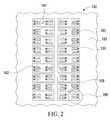
- FIG. 2is a fragmentary view of the first surface of the midplane board 100 .
- the midplane board 100has a plurality of surface contact elements. More specifically, the surface contact elements are essentially planar contact pads 106 made of conductive material such as copper, gold, silver or any other material that is suitable for conveying an electrical signal.
- the contact pads 106are comprised of copper and are plated with hard nickel and hard gold.
- the hard nickel and hard goldallows the surface oxidation of the copper to be substantially avoided and general surface wear to be reduced.
- the contact pads 106are of oblong shape in order to increase the contact surface area and thus facilitate registration with the contact elements from the circuit boards as well as compensate for wiping action that may occur when a circuit board is brought in contact with midplane board 100 .
- Each contact pad 106is associated with a respective microvia 104 for transporting electrical signals through the midplane board 100 .
- microvias and buried viasare fairly well known in the art, a specific implementation will be herein described for the sake of clarity.
- microviasare holes in the midplane board that are plated with a conductive material such as copper and which interconnect one external surface of the midplane board 100 to one or more of its internal layers and/or the opposite external surface.
- Buried viaswhich will be described hereinafter with reference to a subsequent figure, have a similar structure than that of microvias but interconnect one or more internal layers of the midplane board and do not extend to any one of the external surfaces of the main board 100 .
- Microvias and buried viasare typically fabricated using a laser drilling process and, alternatively, by using a mechanical drilling process.
- a laser drilling processFor more information on the fabrication of vias, the reader is invited to consult the paper entitled “Introducing Via-in-Pad Blind Via Technology to Any PCB Multilayer Fabricator” by L. W. Burgess, which was presented at the IPC Printed Circuits Expo in March of 1997. The contents of this paper are hereby incorporated by reference.
- the microvias 104are capable of channeling electrical signals into an interior layer of the midplane board 100 .
- FIG. 2further shows that the contact pads 106 and their corresponding microvias 104 are coupled in pairs 108 .
- Each pair 108carries a differential signal.
- a differential signalexpresses information as a difference between two values. Thus, all signals are expressed in relative fashion (i.e., as a function of one another) and the adverse impact associated with extreme voltage variations is thereby avoided. Further advantages associated with the use of a differential pair reside in the reduction of cross talk and an improved rejection of common-mode electrical noise. Furthermore, creating a differential signal also lessens the ground drop.
- FIG. 2shows that the microvias are regrouped into differential pairs, it should be expressly understood that single ended signals can be used without detracting from the spirit of the invention.
- ground plane 103A significant portion of each external surface of the midplane board 100 is covered by a ground plane 103 .
- the ground planeis a conductive coating or layer, typically made of copper foil.
- the ground plane 103has ground clearances or ground voids 102 where the contact pads 106 and the respective microvias 104 are located. Thus, electrical signals of varying voltages are capable of being conveyed by the contact pads 106 and the microvias 104 .
- the ground clearance 102 depicted in FIG. 2is of approximately rectangular shape, it should be expressly understood that a ground clearance of any shape remains within the scope of this invention.
- FIG. 2also shows that each ground clearance 102 surrounds two microvia pairs 108 . It should be understood, however, that a ground clearance 102 surrounding any number of microvia pairs 108 remains within the scope of this invention.
- FIG. 3is an enlarged fragmentary view of the second surface of the midplane board 100 that is opposite the first surface shown in FIG. 2 .
- the second surfacehas components that are similar to those of the first surface, namely: contact pads 106 , microvias 104 , and ground clearances 102 .
- the main difference between the components on the first and second surfacesresides in their geometrical relationship.
- the components on the first surface and the components on the second surfaceare disposed in rows.
- the rows of contact pads 106are designated 107 in the drawing. In each row 107 , the contact pads 106 are arranged according to two parallel straight lines 107 a , 107 b .
- the lines 107 a , 107 bare parallel within a common row 107 .
- the rows 107 on one main surface of the midplane board 100are parallel to one another.
- the rows 107 on one main surfaceare perpendicular to the rows 107 on the other main surface of the midplane board 100 .
- the contact pads 106 on each line 107 a , 107 bare designed to engage corresponding contact pads 900 formed on the edge 920 of a circuit board 910 , as described in FIG. 9, such that electrical signals can be exchanged between the circuit board 910 and the midplane board 100 .
- FIG. 4also shows how the microvias 104 , 104 ′ on the first and second surfaces of the midplane board 100 are positioned relative to each other. More specifically, the figure shows the components on the first surface in solid lines while the components on the second surface appear in dotted lines.
- FIG. 5is an enlarged fragmentary cross-sectional view of the midplane board 100 .
- the midplane board 100is a six-layer structure and includes a first external layer 602 , a first signal layer 604 below the layer 602 , a first intermediate layer 606 below the layer 604 , a second intermediate layer 608 , a second signal layer 610 and a second external layer 612 .
- Each of the first and second external layers 602 , 612carries the surface contact elements, namely the contact pads 106 106 ′.
- the contact pads 106 106 ′ on the external layer 602 and the second external layer 612are connected, via the microvias 104 104 ′, to the first and second signal layers 604 , 610 respectively.
- first and the second signal layers 604 and 610connect to one another through buried vias 614 .
- an electrical connectionis realized between contact pads 106 and 106 ′.
- Each of the first and second external layers 602 , 612is adapted to receive circuit boards. Hence, electrical signals can be conveyed, via the interior midplane board 100 , between circuit boards located on opposite surfaces of a midplane board 100 .
- FIG. 5further shows that the midplane board 100 comprises several through vias 644 (only one is shown in the figure) operative to maintain the first and second surfaces 602 , 612 at a common ground voltage level by interconnecting the ground planes 103 , 103 ′ to one another.
- the purpose of the first and second intermediary layers 606 608is to provide power distribution.
- the first intermediary layer 606connects to the positive terminal of a power supply (such as a battery) while the second intermediate layer 608 connects to the negative terminal of the power supply.
- the midplane board 100as comprising a power layer and a power return layer
- intermediary layerssuch as two ground layers
- the first and second intermediary layers 606are ground layers 608 having localized perforations or a mesh configuration in the areas about the contact pads 106 106 ′. In certain cases the use of such localized perforations can reduce stray capacitances between the contact pads.
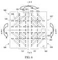
- FIG. 6is a schematic diagram of the connection paths within the midplane board 100 to connect the microvias 104 104 ′, hence the contact pads 106 106 ′, on the first surface of the midplane board 100 to those on the second surface at an intersect area. Note that for clarity, the contact pads 106 , 106 ′ have not been shown in FIG. 6 .
- Signal connection paths 25link the microvias 104 to microvias 104 ′ and, in doing so, define a certain pattern.
- the intersect areais subdivided into four quadrants, namely: a first quadrant 500 , a second quadrant 502 , a third quadrant 504 , and a fourth quadrant 506 where this pattern is repeated which has the advantage of reducing design time.
- a pattern of the signal connection paths 25is created in the first quadrant 500 .
- the patternis then subsequently reproduced onto the second quadrant 502 by taking a mirror image along line A—A.
- the pattern in the first and second quadrantsis then reproduced by taking a mirror image along line B—B to create the connections in the third and fourth quadrants 504 506 .
- FIG. 7illustrates in greater detail how the microvias 104 are connected to the microvias 104 ′ at an intersect area in accordance with a specific example of implementation of the invention.
- the intersect areais divided into four quadrants, namely: a first quadrant 500 ′, a second quadrant 502 ′, a third quadrant 504 ′, and a fourth quadrant 506 ′.
- Microvias 104 , 104 ′ within a quadrant, such as the first quadrant 500 ′,are connected by means of signal connection paths including buried vias 614 and conductive pathways 508 formed on the first and second signal layers 604 , 610 .
- a plurality of conductive pathways 508are formed on the first signal layer 604 that connect the microvias 104 to the respective buried vias 614 .
- the buried vias 614connect the first signal layer 604 to the second signal layer 610 .
- the conductive pathway 508 ′(shown in dotted lines) on the second signal layer 610 connects the buried vias 614 to the microvias 104 ′.
- the pattern in the first quadrantis reproduced onto the second quadrant 502 ′ by taking a mirror image along line A′—A′.
- the pattern in the first and second quadrants 500 ′ 502 ′is then reproduced by taking a mirror image along line B′—B′.
- the four quadrants 500 ′ 502 ′ 504 ′ 506 ′therefore form a unique pattern tile 600 .
- the pattern tile 600as shown in FIG. 8, is repeated on the entire surface of the midplane board 800 . This modular approach reduces the design cost and production time by avoiding the duplication of layout work.
Landscapes
- Engineering & Computer Science (AREA)
- Microelectronics & Electronic Packaging (AREA)
- Combinations Of Printed Boards (AREA)
Abstract
Description
Claims (24)
Priority Applications (1)
| Application Number | Priority Date | Filing Date | Title |
|---|---|---|---|
| US09/639,075US6528737B1 (en) | 2000-08-16 | 2000-08-16 | Midplane configuration featuring surface contact connectors |
Applications Claiming Priority (1)
| Application Number | Priority Date | Filing Date | Title |
|---|---|---|---|
| US09/639,075US6528737B1 (en) | 2000-08-16 | 2000-08-16 | Midplane configuration featuring surface contact connectors |
Publications (1)
| Publication Number | Publication Date |
|---|---|
| US6528737B1true US6528737B1 (en) | 2003-03-04 |
Family
ID=24562625
Family Applications (1)
| Application Number | Title | Priority Date | Filing Date |
|---|---|---|---|
| US09/639,075Expired - LifetimeUS6528737B1 (en) | 2000-08-16 | 2000-08-16 | Midplane configuration featuring surface contact connectors |
Country Status (1)
| Country | Link |
|---|---|
| US (1) | US6528737B1 (en) |
Cited By (63)
| Publication number | Priority date | Publication date | Assignee | Title |
|---|---|---|---|---|
| US20030002541A1 (en)* | 2001-06-07 | 2003-01-02 | Fowler Michael L. | Mid-connect architecture with point-to-point connections for high speed data transfer |
| US20030142483A1 (en)* | 2002-01-30 | 2003-07-31 | Ofer Iny | Switching device and a method for the configuration thereof |
| US20040023558A1 (en)* | 2001-06-07 | 2004-02-05 | Fowler Michael L. | Mid-connect architecture with point-to-point connections for high speed data transfer |
| US6717825B2 (en)* | 2002-01-18 | 2004-04-06 | Fci Americas Technology, Inc. | Electrical connection system for two printed circuit boards mounted on opposite sides of a mid-plane printed circuit board at angles to each other |
| US20040130861A1 (en)* | 2003-01-03 | 2004-07-08 | Dell Products L.P. | PCB as a structural component and internal chassis alignment |
| USD493152S1 (en) | 2002-11-27 | 2004-07-20 | International Business Machines Corporation | Server blade chassis midplane printed circuit board with cover |
| US20040238213A1 (en)* | 2003-05-28 | 2004-12-02 | Pitio Walter Michael | Uniform impedance printed circuit board |
| US20050109532A1 (en)* | 2003-07-08 | 2005-05-26 | Hermkens Gerald A. | Method for manufacturing a sequential backplane |
| US20050117317A1 (en)* | 2003-11-28 | 2005-06-02 | Warburton Kenneth J. | Bridged parallel distributing frame |
| US6903939B1 (en)* | 2002-04-19 | 2005-06-07 | Turnstone Systems, Inc. | Physical architecture for design of high density metallic cross connect systems |
| US20050161254A1 (en)* | 2004-01-26 | 2005-07-28 | Litton Systems, Inc. | Multilayered circuit board for high-speed, differential signals |
| US20050202722A1 (en)* | 2004-02-13 | 2005-09-15 | Regnier Kent E. | Preferential via exit structures with triad configuration for printed circuit boards |
| US20050201065A1 (en)* | 2004-02-13 | 2005-09-15 | Regnier Kent E. | Preferential ground and via exit structures for printed circuit boards |
| US20050280655A1 (en)* | 2004-05-14 | 2005-12-22 | Hutchins Edward A | Kill bit graphics processing system and method |
| US20060024984A1 (en)* | 2004-07-01 | 2006-02-02 | Cohen Thomas S | Midplane especially applicable to an orthogonal architecture electronic system |
| US20060091545A1 (en)* | 2004-10-29 | 2006-05-04 | Casher Patrick R | Printed circuit board for high-speed electrical connectors |
| US20060105596A1 (en)* | 2004-11-12 | 2006-05-18 | Minich Steven E | Two piece mid-plane |
| US20060109960A1 (en)* | 2004-10-25 | 2006-05-25 | D Evelyn Linda K | System and method for unilateral verification of caller location information |
| US20060151869A1 (en)* | 2005-01-10 | 2006-07-13 | Franz Gisin | Printed circuit boards and the like with improved signal integrity for differential signal pairs |
| US20060189212A1 (en)* | 2005-02-22 | 2006-08-24 | Avery Hazelton P | Differential signal connector with wafer-style construction |
| US20070207632A1 (en)* | 2006-03-03 | 2007-09-06 | Fci Americas Technology, Inc. | Midplane with offset connectors |
| US20080026638A1 (en)* | 2004-07-01 | 2008-01-31 | Cohen Thomas S | Differential electrical connector assembly |
| US20080043405A1 (en)* | 2006-08-16 | 2008-02-21 | Tyan Computer Corporation | Chassis partition architecture for multi-processor system |
| US7336502B1 (en)* | 2003-06-03 | 2008-02-26 | Force10 Networks, Inc. | High-speed router with backplane using tuned-impedance thru-holes and vias |
| US20080239687A1 (en)* | 2007-03-29 | 2008-10-02 | Leigh Kevin B | Server infrastructure having independent backplanes to distribute power and to route signals |
| US20090221165A1 (en)* | 2008-02-29 | 2009-09-03 | Buck Jonathan E | Cross talk reduction for high speed electrical connectors |
| US20100048067A1 (en)* | 2007-02-28 | 2010-02-25 | Johnescu Douglas M | Orthogonal header |
| US7762843B2 (en) | 2006-12-19 | 2010-07-27 | Fci Americas Technology, Inc. | Shieldless, high-speed, low-cross-talk electrical connector |
| EP1878326A4 (en)* | 2005-04-07 | 2010-11-03 | Framatome Connectors Int | Orthogonal backplane connector |
| US7914304B2 (en) | 2005-06-30 | 2011-03-29 | Amphenol Corporation | Electrical connector with conductors having diverging portions |
| US20110097934A1 (en)* | 2009-10-28 | 2011-04-28 | Minich Steven E | Electrical connector having ground plates and ground coupling bar |
| US20110117781A1 (en)* | 2009-11-13 | 2011-05-19 | Stoner Stuart C | Attachment system for electrical connector |
| US20110230095A1 (en)* | 2005-06-30 | 2011-09-22 | Amphenol Corporation | High frequency electrical connector |
| US8060682B1 (en)* | 2008-11-14 | 2011-11-15 | Qlogic, Corporation | Method and system for multi-level switch configuration |
| CN102695393A (en)* | 2012-05-04 | 2012-09-26 | 华为技术有限公司 | Perpendicular orthogonal interconnection system and communication device |
| US20130010786A1 (en)* | 2011-07-08 | 2013-01-10 | Cisco Technology, Inc. | System and Method for High Connectivity Platform |
| US8444436B1 (en) | 2004-07-01 | 2013-05-21 | Amphenol Corporation | Midplane especially applicable to an orthogonal architecture electronic system |
| US8491313B2 (en) | 2011-02-02 | 2013-07-23 | Amphenol Corporation | Mezzanine connector |
| USD718253S1 (en) | 2012-04-13 | 2014-11-25 | Fci Americas Technology Llc | Electrical cable connector |
| US8905651B2 (en) | 2012-01-31 | 2014-12-09 | Fci | Dismountable optical coupling device |
| USD720698S1 (en) | 2013-03-15 | 2015-01-06 | Fci Americas Technology Llc | Electrical cable connector |
| US8944831B2 (en) | 2012-04-13 | 2015-02-03 | Fci Americas Technology Llc | Electrical connector having ribbed ground plate with engagement members |
| USD727268S1 (en) | 2012-04-13 | 2015-04-21 | Fci Americas Technology Llc | Vertical electrical connector |
| USD727852S1 (en) | 2012-04-13 | 2015-04-28 | Fci Americas Technology Llc | Ground shield for a right angle electrical connector |
| US9048583B2 (en) | 2009-03-19 | 2015-06-02 | Fci Americas Technology Llc | Electrical connector having ribbed ground plate |
| USD733662S1 (en) | 2013-01-25 | 2015-07-07 | Fci Americas Technology Llc | Connector housing for electrical connector |
| USD746236S1 (en) | 2012-07-11 | 2015-12-29 | Fci Americas Technology Llc | Electrical connector housing |
| US9257778B2 (en) | 2012-04-13 | 2016-02-09 | Fci Americas Technology | High speed electrical connector |
| US9277649B2 (en) | 2009-02-26 | 2016-03-01 | Fci Americas Technology Llc | Cross talk reduction for high-speed electrical connectors |
| US9543703B2 (en) | 2012-07-11 | 2017-01-10 | Fci Americas Technology Llc | Electrical connector with reduced stack height |
| US9697160B2 (en)* | 2014-12-23 | 2017-07-04 | Intel Corporation | Midplane interconnect system with conductor twist mitigation |
| US11444397B2 (en) | 2015-07-07 | 2022-09-13 | Amphenol Fci Asia Pte. Ltd. | Electrical connector with cavity between terminals |
| US11469554B2 (en) | 2020-01-27 | 2022-10-11 | Fci Usa Llc | High speed, high density direct mate orthogonal connector |
| US11522310B2 (en) | 2012-08-22 | 2022-12-06 | Amphenol Corporation | High-frequency electrical connector |
| US11539171B2 (en) | 2016-08-23 | 2022-12-27 | Amphenol Corporation | Connector configurable for high performance |
| US11715914B2 (en) | 2014-01-22 | 2023-08-01 | Amphenol Corporation | High speed, high density electrical connector with shielded signal paths |
| US11757215B2 (en) | 2018-09-26 | 2023-09-12 | Amphenol East Asia Electronic Technology (Shenzhen) Co., Ltd. | High speed electrical connector and printed circuit board thereof |
| US11757224B2 (en) | 2010-05-07 | 2023-09-12 | Amphenol Corporation | High performance cable connector |
| US11799246B2 (en) | 2020-01-27 | 2023-10-24 | Fci Usa Llc | High speed connector |
| US11817655B2 (en) | 2020-09-25 | 2023-11-14 | Amphenol Commercial Products (Chengdu) Co., Ltd. | Compact, high speed electrical connector |
| US11942716B2 (en) | 2020-09-22 | 2024-03-26 | Amphenol Commercial Products (Chengdu) Co., Ltd. | High speed electrical connector |
| US12300936B2 (en) | 2019-02-19 | 2025-05-13 | Amphenol Corporation | High speed connector |
| US12300920B2 (en) | 2021-08-13 | 2025-05-13 | Amphenol Commercial Products (Chengdu) Co., Ltd. | High performance card edge connector for high bandwidth transmission |
Citations (6)
| Publication number | Priority date | Publication date | Assignee | Title |
|---|---|---|---|---|
| US5455742A (en)* | 1994-03-21 | 1995-10-03 | Eaton Corporation | Direct circuit board connection |
| US5887158A (en) | 1992-06-08 | 1999-03-23 | Quickturn Design Systems, Inc. | Switching midplane and interconnecting system for interconnecting large numbers of signals |
| US5949656A (en)* | 1994-06-01 | 1999-09-07 | Davox Corporation | Electronic assembly interconnection system |
| US6058019A (en)* | 1998-05-21 | 2000-05-02 | International Business Machines Corporation | Electronic circuit card assembly having confined ground path return |
| US6328572B1 (en)* | 1999-07-28 | 2001-12-11 | Kel Corporation | Motherboard with board having terminating resistance |
| US6335867B1 (en)* | 1997-08-08 | 2002-01-01 | Hitachi, Ltd. | Apparatus for interconnecting logic boards |
- 2000
- 2000-08-16USUS09/639,075patent/US6528737B1/ennot_activeExpired - Lifetime
Patent Citations (6)
| Publication number | Priority date | Publication date | Assignee | Title |
|---|---|---|---|---|
| US5887158A (en) | 1992-06-08 | 1999-03-23 | Quickturn Design Systems, Inc. | Switching midplane and interconnecting system for interconnecting large numbers of signals |
| US5455742A (en)* | 1994-03-21 | 1995-10-03 | Eaton Corporation | Direct circuit board connection |
| US5949656A (en)* | 1994-06-01 | 1999-09-07 | Davox Corporation | Electronic assembly interconnection system |
| US6335867B1 (en)* | 1997-08-08 | 2002-01-01 | Hitachi, Ltd. | Apparatus for interconnecting logic boards |
| US6058019A (en)* | 1998-05-21 | 2000-05-02 | International Business Machines Corporation | Electronic circuit card assembly having confined ground path return |
| US6328572B1 (en)* | 1999-07-28 | 2001-12-11 | Kel Corporation | Motherboard with board having terminating resistance |
Non-Patent Citations (1)
| Title |
|---|
| Larry W. Burgess, Introducing Via-in-Pad Blind Via Technology to Any PCB Multilayer Fabricator, The Institute for Interconnecting and Packaging Electronic Circuits, Mar. 9-13, 1997 pp S15-2-1 to S15-2-4. |
Cited By (143)
| Publication number | Priority date | Publication date | Assignee | Title |
|---|---|---|---|---|
| US20040023558A1 (en)* | 2001-06-07 | 2004-02-05 | Fowler Michael L. | Mid-connect architecture with point-to-point connections for high speed data transfer |
| US20030002541A1 (en)* | 2001-06-07 | 2003-01-02 | Fowler Michael L. | Mid-connect architecture with point-to-point connections for high speed data transfer |
| US6717825B2 (en)* | 2002-01-18 | 2004-04-06 | Fci Americas Technology, Inc. | Electrical connection system for two printed circuit boards mounted on opposite sides of a mid-plane printed circuit board at angles to each other |
| US20030142483A1 (en)* | 2002-01-30 | 2003-07-31 | Ofer Iny | Switching device and a method for the configuration thereof |
| US6711028B2 (en)* | 2002-01-30 | 2004-03-23 | Dune Networks | Switching device and a method for the configuration thereof |
| US6903939B1 (en)* | 2002-04-19 | 2005-06-07 | Turnstone Systems, Inc. | Physical architecture for design of high density metallic cross connect systems |
| USD493152S1 (en) | 2002-11-27 | 2004-07-20 | International Business Machines Corporation | Server blade chassis midplane printed circuit board with cover |
| US6847521B2 (en) | 2003-01-03 | 2005-01-25 | Dell Products L.P. | PCB as a structural component and internal chassis alignment |
| US20040130861A1 (en)* | 2003-01-03 | 2004-07-08 | Dell Products L.P. | PCB as a structural component and internal chassis alignment |
| US20040238213A1 (en)* | 2003-05-28 | 2004-12-02 | Pitio Walter Michael | Uniform impedance printed circuit board |
| US7336502B1 (en)* | 2003-06-03 | 2008-02-26 | Force10 Networks, Inc. | High-speed router with backplane using tuned-impedance thru-holes and vias |
| US20050109532A1 (en)* | 2003-07-08 | 2005-05-26 | Hermkens Gerald A. | Method for manufacturing a sequential backplane |
| US7172805B2 (en) | 2003-07-08 | 2007-02-06 | Viasytems Group, Inc. | Method for manufacturing a sequential backplane |
| US20060278430A1 (en)* | 2003-07-08 | 2006-12-14 | Viasystems Group, Inc. | Method for manufacturing a midplane |
| US20050117317A1 (en)* | 2003-11-28 | 2005-06-02 | Warburton Kenneth J. | Bridged parallel distributing frame |
| US7304865B2 (en)* | 2003-11-28 | 2007-12-04 | Warburton Kenneth J | Bridged parallel distributing frame |
| US8364444B2 (en) | 2003-11-28 | 2013-01-29 | Warburton Kenneth J | Method for designing distributing frame |
| US8639478B2 (en) | 2003-11-28 | 2014-01-28 | Kenneth J. Warburton | Method for designing distributing frame |
| US20080077646A1 (en)* | 2003-11-28 | 2008-03-27 | Warburton Kenneth J | Method for designing distributing frame |
| WO2005074336A3 (en)* | 2004-01-26 | 2005-10-06 | Litton Systems Inc | Multilayered circuit board for high-speed, differential signals |
| US20050161254A1 (en)* | 2004-01-26 | 2005-07-28 | Litton Systems, Inc. | Multilayered circuit board for high-speed, differential signals |
| US7057115B2 (en)* | 2004-01-26 | 2006-06-06 | Litton Systems, Inc. | Multilayered circuit board for high-speed, differential signals |
| US20050201065A1 (en)* | 2004-02-13 | 2005-09-15 | Regnier Kent E. | Preferential ground and via exit structures for printed circuit boards |
| US7448909B2 (en) | 2004-02-13 | 2008-11-11 | Molex Incorporated | Preferential via exit structures with triad configuration for printed circuit boards |
| US20080318450A1 (en)* | 2004-02-13 | 2008-12-25 | Molex Incorporated | Preferential via exit structures with triad configuration for printed circuit boards |
| US7633766B2 (en) | 2004-02-13 | 2009-12-15 | Molex Incorporated | Preferential via exit structures with triad configuration for printed circuit boards |
| US20050202722A1 (en)* | 2004-02-13 | 2005-09-15 | Regnier Kent E. | Preferential via exit structures with triad configuration for printed circuit boards |
| US20050280655A1 (en)* | 2004-05-14 | 2005-12-22 | Hutchins Edward A | Kill bit graphics processing system and method |
| US9106020B2 (en)* | 2004-07-01 | 2015-08-11 | Amphenol Corporation | Midplane especially applicable to an orthogonal architecture electronic system |
| US7744415B2 (en) | 2004-07-01 | 2010-06-29 | Amphenol Corporation | Midplane especially applicable to an orthogonal architecture electronic system |
| US20110130038A1 (en)* | 2004-07-01 | 2011-06-02 | Cohen Thomas S | Differential electrical connector assembly |
| US8202118B2 (en) | 2004-07-01 | 2012-06-19 | Amphenol Corporation | Differential electrical connector assembly |
| US7108556B2 (en)* | 2004-07-01 | 2006-09-19 | Amphenol Corporation | Midplane especially applicable to an orthogonal architecture electronic system |
| US20110076860A1 (en)* | 2004-07-01 | 2011-03-31 | Cohen Thomas S | Midplane especially applicable to an orthogonal architecture electronic system |
| US20060024984A1 (en)* | 2004-07-01 | 2006-02-02 | Cohen Thomas S | Midplane especially applicable to an orthogonal architecture electronic system |
| US20080026638A1 (en)* | 2004-07-01 | 2008-01-31 | Cohen Thomas S | Differential electrical connector assembly |
| US8226438B2 (en) | 2004-07-01 | 2012-07-24 | Amphenol Corporation | Midplane especially applicable to an orthogonal architecture electronic system |
| US7811130B2 (en) | 2004-07-01 | 2010-10-12 | Amphenol Corporation | Differential electrical connector assembly |
| US20070149057A1 (en)* | 2004-07-01 | 2007-06-28 | Amphenol Corpoation | Midplane especially applicable to an orthogonal architecture electronic system |
| US8444436B1 (en) | 2004-07-01 | 2013-05-21 | Amphenol Corporation | Midplane especially applicable to an orthogonal architecture electronic system |
| US7422484B2 (en)* | 2004-07-01 | 2008-09-09 | Amphenol Corporation | Midplane especially applicable to an orthogonal architecture electronic system |
| US20130337665A1 (en)* | 2004-07-01 | 2013-12-19 | Amphenol Corporation | Midplane Especially Applicable to an Orthogonal Architecture Electronic System |
| US7544096B2 (en) | 2004-07-01 | 2009-06-09 | Amphenol Corporation | Differential electrical connector assembly |
| US20090061684A1 (en)* | 2004-07-01 | 2009-03-05 | Amphenol Corporation | Midplane especially applicable to an orthogonal architecture electronic system |
| US20060109960A1 (en)* | 2004-10-25 | 2006-05-25 | D Evelyn Linda K | System and method for unilateral verification of caller location information |
| US7645944B2 (en) | 2004-10-29 | 2010-01-12 | Molex Incorporated | Printed circuit board for high-speed electrical connectors |
| US20060091545A1 (en)* | 2004-10-29 | 2006-05-04 | Casher Patrick R | Printed circuit board for high-speed electrical connectors |
| KR100904143B1 (en) | 2004-10-29 | 2009-06-24 | 몰렉스 인코포레이티드 | Printed circuit board for high-speed electrical connectors |
| WO2006050202A1 (en)* | 2004-10-29 | 2006-05-11 | Molex Incorporated | Printed circuit board for high-speed electrical connectors |
| US20060105596A1 (en)* | 2004-11-12 | 2006-05-18 | Minich Steven E | Two piece mid-plane |
| US7052288B1 (en) | 2004-11-12 | 2006-05-30 | Fci Americas Technology, Inc. | Two piece mid-plane |
| EP1831970A4 (en)* | 2004-12-24 | 2013-04-24 | Amphenol Corp | Midplane epecially applicable to an ortogonal architecture electronic system |
| US20060151869A1 (en)* | 2005-01-10 | 2006-07-13 | Franz Gisin | Printed circuit boards and the like with improved signal integrity for differential signal pairs |
| US20070294890A1 (en)* | 2005-01-10 | 2007-12-27 | Sanmina-Sci Corporation | Printed circuit boards and the like with improved signal integrity for differential signal pairs |
| WO2007061429A3 (en)* | 2005-01-10 | 2007-10-04 | Sanmina Sci Corp | Printed circuit boards and the like with improved signal integrity for differential signal pairs |
| US20090011620A1 (en)* | 2005-02-22 | 2009-01-08 | Molex Incorporated | Differential signal connector with wafer-style construction |
| US7422483B2 (en) | 2005-02-22 | 2008-09-09 | Molex Incorproated | Differential signal connector with wafer-style construction |
| US7534142B2 (en) | 2005-02-22 | 2009-05-19 | Molex Incorporated | Differential signal connector with wafer-style construction |
| US20060189212A1 (en)* | 2005-02-22 | 2006-08-24 | Avery Hazelton P | Differential signal connector with wafer-style construction |
| US20080009147A1 (en)* | 2005-02-22 | 2008-01-10 | Avery Hazelton P | Circuit board via arrangement for differential signal connector |
| EP1878326A4 (en)* | 2005-04-07 | 2010-11-03 | Framatome Connectors Int | Orthogonal backplane connector |
| US8215968B2 (en) | 2005-06-30 | 2012-07-10 | Amphenol Corporation | Electrical connector with signal conductor pairs having offset contact portions |
| US7914304B2 (en) | 2005-06-30 | 2011-03-29 | Amphenol Corporation | Electrical connector with conductors having diverging portions |
| US9219335B2 (en) | 2005-06-30 | 2015-12-22 | Amphenol Corporation | High frequency electrical connector |
| US20110230095A1 (en)* | 2005-06-30 | 2011-09-22 | Amphenol Corporation | High frequency electrical connector |
| US8864521B2 (en) | 2005-06-30 | 2014-10-21 | Amphenol Corporation | High frequency electrical connector |
| US9705255B2 (en) | 2005-06-30 | 2017-07-11 | Amphenol Corporation | High frequency electrical connector |
| US20070207632A1 (en)* | 2006-03-03 | 2007-09-06 | Fci Americas Technology, Inc. | Midplane with offset connectors |
| US20080043405A1 (en)* | 2006-08-16 | 2008-02-21 | Tyan Computer Corporation | Chassis partition architecture for multi-processor system |
| US7762843B2 (en) | 2006-12-19 | 2010-07-27 | Fci Americas Technology, Inc. | Shieldless, high-speed, low-cross-talk electrical connector |
| US8382521B2 (en) | 2006-12-19 | 2013-02-26 | Fci Americas Technology Llc | Shieldless, high-speed, low-cross-talk electrical connector |
| US8096832B2 (en) | 2006-12-19 | 2012-01-17 | Fci Americas Technology Llc | Shieldless, high-speed, low-cross-talk electrical connector |
| US20100291806A1 (en)* | 2006-12-19 | 2010-11-18 | Minich Steven E | Shieldless, High-Speed, Low-Cross-Talk Electrical Connector |
| US8678860B2 (en) | 2006-12-19 | 2014-03-25 | Fci Americas Technology Llc | Shieldless, high-speed, low-cross-talk electrical connector |
| US7967647B2 (en)* | 2007-02-28 | 2011-06-28 | Fci Americas Technology Llc | Orthogonal header |
| US20100048067A1 (en)* | 2007-02-28 | 2010-02-25 | Johnescu Douglas M | Orthogonal header |
| US8057267B2 (en) | 2007-02-28 | 2011-11-15 | Fci Americas Technology Llc | Orthogonal header |
| US20110113625A1 (en)* | 2007-02-28 | 2011-05-19 | Fci Americas Technology, Inc. | Orthogonal header |
| US8009438B2 (en)* | 2007-03-29 | 2011-08-30 | Hewlett-Packard Development Company, L.P. | Server infrastructure having independent backplanes to distribute power and to route signals |
| US20080239687A1 (en)* | 2007-03-29 | 2008-10-02 | Leigh Kevin B | Server infrastructure having independent backplanes to distribute power and to route signals |
| US20090221165A1 (en)* | 2008-02-29 | 2009-09-03 | Buck Jonathan E | Cross talk reduction for high speed electrical connectors |
| US8764464B2 (en) | 2008-02-29 | 2014-07-01 | Fci Americas Technology Llc | Cross talk reduction for high speed electrical connectors |
| US8060682B1 (en)* | 2008-11-14 | 2011-11-15 | Qlogic, Corporation | Method and system for multi-level switch configuration |
| US9277649B2 (en) | 2009-02-26 | 2016-03-01 | Fci Americas Technology Llc | Cross talk reduction for high-speed electrical connectors |
| US9461410B2 (en) | 2009-03-19 | 2016-10-04 | Fci Americas Technology Llc | Electrical connector having ribbed ground plate |
| US10096921B2 (en) | 2009-03-19 | 2018-10-09 | Fci Usa Llc | Electrical connector having ribbed ground plate |
| US10720721B2 (en) | 2009-03-19 | 2020-07-21 | Fci Usa Llc | Electrical connector having ribbed ground plate |
| US9048583B2 (en) | 2009-03-19 | 2015-06-02 | Fci Americas Technology Llc | Electrical connector having ribbed ground plate |
| US20110097934A1 (en)* | 2009-10-28 | 2011-04-28 | Minich Steven E | Electrical connector having ground plates and ground coupling bar |
| US8267721B2 (en) | 2009-10-28 | 2012-09-18 | Fci Americas Technology Llc | Electrical connector having ground plates and ground coupling bar |
| US8616919B2 (en) | 2009-11-13 | 2013-12-31 | Fci Americas Technology Llc | Attachment system for electrical connector |
| US20110117781A1 (en)* | 2009-11-13 | 2011-05-19 | Stoner Stuart C | Attachment system for electrical connector |
| US11757224B2 (en) | 2010-05-07 | 2023-09-12 | Amphenol Corporation | High performance cable connector |
| US8657627B2 (en) | 2011-02-02 | 2014-02-25 | Amphenol Corporation | Mezzanine connector |
| US8491313B2 (en) | 2011-02-02 | 2013-07-23 | Amphenol Corporation | Mezzanine connector |
| US8636543B2 (en) | 2011-02-02 | 2014-01-28 | Amphenol Corporation | Mezzanine connector |
| US8801464B2 (en) | 2011-02-02 | 2014-08-12 | Amphenol Corporation | Mezzanine connector |
| US20130010786A1 (en)* | 2011-07-08 | 2013-01-10 | Cisco Technology, Inc. | System and Method for High Connectivity Platform |
| US9039432B2 (en)* | 2011-07-08 | 2015-05-26 | Cisco Technology, Inc. | System and method for high connectivity platform |
| US8905651B2 (en) | 2012-01-31 | 2014-12-09 | Fci | Dismountable optical coupling device |
| USD790471S1 (en) | 2012-04-13 | 2017-06-27 | Fci Americas Technology Llc | Vertical electrical connector |
| US9831605B2 (en) | 2012-04-13 | 2017-11-28 | Fci Americas Technology Llc | High speed electrical connector |
| USD816044S1 (en) | 2012-04-13 | 2018-04-24 | Fci Americas Technology Llc | Electrical cable connector |
| USD727852S1 (en) | 2012-04-13 | 2015-04-28 | Fci Americas Technology Llc | Ground shield for a right angle electrical connector |
| USD718253S1 (en) | 2012-04-13 | 2014-11-25 | Fci Americas Technology Llc | Electrical cable connector |
| USD748063S1 (en) | 2012-04-13 | 2016-01-26 | Fci Americas Technology Llc | Electrical ground shield |
| US9257778B2 (en) | 2012-04-13 | 2016-02-09 | Fci Americas Technology | High speed electrical connector |
| USD750030S1 (en) | 2012-04-13 | 2016-02-23 | Fci Americas Technology Llc | Electrical cable connector |
| USD750025S1 (en) | 2012-04-13 | 2016-02-23 | Fci Americas Technology Llc | Vertical electrical connector |
| US8944831B2 (en) | 2012-04-13 | 2015-02-03 | Fci Americas Technology Llc | Electrical connector having ribbed ground plate with engagement members |
| USD727268S1 (en) | 2012-04-13 | 2015-04-21 | Fci Americas Technology Llc | Vertical electrical connector |
| CN102695393B (en)* | 2012-05-04 | 2014-11-05 | 华为技术有限公司 | Perpendicular orthogonal interconnection system and communication device |
| CN102695393A (en)* | 2012-05-04 | 2012-09-26 | 华为技术有限公司 | Perpendicular orthogonal interconnection system and communication device |
| US10084255B2 (en) | 2012-05-04 | 2018-09-25 | Huawei Technologies Co., Ltd | Perpendicular and orthogonal interconnection system and communications device |
| US9532471B2 (en) | 2012-05-04 | 2016-12-27 | Huawei Technologies Co., Ltd. | Perpendicular and orthogonal interconnection system and communications device |
| WO2013163867A1 (en)* | 2012-05-04 | 2013-11-07 | 华为技术有限公司 | Vertical orthogonal interconnection system and communication device |
| US9543703B2 (en) | 2012-07-11 | 2017-01-10 | Fci Americas Technology Llc | Electrical connector with reduced stack height |
| US9871323B2 (en) | 2012-07-11 | 2018-01-16 | Fci Americas Technology Llc | Electrical connector with reduced stack height |
| USD746236S1 (en) | 2012-07-11 | 2015-12-29 | Fci Americas Technology Llc | Electrical connector housing |
| USD751507S1 (en) | 2012-07-11 | 2016-03-15 | Fci Americas Technology Llc | Electrical connector |
| US11901663B2 (en) | 2012-08-22 | 2024-02-13 | Amphenol Corporation | High-frequency electrical connector |
| US11522310B2 (en) | 2012-08-22 | 2022-12-06 | Amphenol Corporation | High-frequency electrical connector |
| USD766832S1 (en) | 2013-01-25 | 2016-09-20 | Fci Americas Technology Llc | Electrical connector |
| USD745852S1 (en) | 2013-01-25 | 2015-12-22 | Fci Americas Technology Llc | Electrical connector |
| USD772168S1 (en) | 2013-01-25 | 2016-11-22 | Fci Americas Technology Llc | Connector housing for electrical connector |
| USD733662S1 (en) | 2013-01-25 | 2015-07-07 | Fci Americas Technology Llc | Connector housing for electrical connector |
| USD720698S1 (en) | 2013-03-15 | 2015-01-06 | Fci Americas Technology Llc | Electrical cable connector |
| US11715914B2 (en) | 2014-01-22 | 2023-08-01 | Amphenol Corporation | High speed, high density electrical connector with shielded signal paths |
| US9954295B2 (en) | 2014-12-23 | 2018-04-24 | Intel Corporation | Midplane interconnect system with conductor twist mitigation |
| US9697160B2 (en)* | 2014-12-23 | 2017-07-04 | Intel Corporation | Midplane interconnect system with conductor twist mitigation |
| US11444397B2 (en) | 2015-07-07 | 2022-09-13 | Amphenol Fci Asia Pte. Ltd. | Electrical connector with cavity between terminals |
| US11955742B2 (en) | 2015-07-07 | 2024-04-09 | Amphenol Fci Asia Pte. Ltd. | Electrical connector with cavity between terminals |
| US11539171B2 (en) | 2016-08-23 | 2022-12-27 | Amphenol Corporation | Connector configurable for high performance |
| US12341301B2 (en) | 2016-08-23 | 2025-06-24 | Amphenol Corporation | Connector configurable for high performance |
| US11757215B2 (en) | 2018-09-26 | 2023-09-12 | Amphenol East Asia Electronic Technology (Shenzhen) Co., Ltd. | High speed electrical connector and printed circuit board thereof |
| US12300936B2 (en) | 2019-02-19 | 2025-05-13 | Amphenol Corporation | High speed connector |
| US11469553B2 (en) | 2020-01-27 | 2022-10-11 | Fci Usa Llc | High speed connector |
| US11799246B2 (en) | 2020-01-27 | 2023-10-24 | Fci Usa Llc | High speed connector |
| US11817657B2 (en) | 2020-01-27 | 2023-11-14 | Fci Usa Llc | High speed, high density direct mate orthogonal connector |
| US11469554B2 (en) | 2020-01-27 | 2022-10-11 | Fci Usa Llc | High speed, high density direct mate orthogonal connector |
| US11942716B2 (en) | 2020-09-22 | 2024-03-26 | Amphenol Commercial Products (Chengdu) Co., Ltd. | High speed electrical connector |
| US11817655B2 (en) | 2020-09-25 | 2023-11-14 | Amphenol Commercial Products (Chengdu) Co., Ltd. | Compact, high speed electrical connector |
| US12300920B2 (en) | 2021-08-13 | 2025-05-13 | Amphenol Commercial Products (Chengdu) Co., Ltd. | High performance card edge connector for high bandwidth transmission |
Similar Documents
| Publication | Publication Date | Title |
|---|---|---|
| US6528737B1 (en) | Midplane configuration featuring surface contact connectors | |
| US11742620B2 (en) | High-frequency electrical connector | |
| US11805595B2 (en) | Backplane footprint for high speed, high density electrical connectors | |
| US6494734B1 (en) | High density electrical connector assembly | |
| US9986634B2 (en) | Circuit board via configurations for high frequency signaling | |
| EP1831970B1 (en) | Midplane especially applicable to an orthogonal architecture electronic system | |
| US3333225A (en) | Connector | |
| CN101950893B (en) | Differential electrical connector assembly | |
| US7508681B2 (en) | Printed circuit board for high speed, high density electrical connector with improved cross-talk minimization attenuation and impedance mismatch characteristics | |
| US20060073709A1 (en) | High density midplane | |
| US6287132B1 (en) | Connector with staggered contact design | |
| US6824393B2 (en) | Fragmented backplane system for I/O applications | |
| US6780059B1 (en) | High speed, high density electrical connector | |
| US20020071260A1 (en) | Electronic board assembly including two elementary boards each carrying connectors on an edge thereof | |
| CN107408786A (en) | Companion backplanes for high-speed, high-density electrical connectors | |
| US6024587A (en) | High speed circuit interconnection apparatus | |
| US4772864A (en) | Multilayer circuit prototyping board | |
| KR20020042712A (en) | A shielded carrier for land grid array connectors and a process for fabricating same | |
| US4814857A (en) | Circuit module with separate signal and power connectors | |
| US20080025007A1 (en) | Partially plated through-holes and achieving high connectivity in multilayer circuit boards using the same | |
| US7359214B2 (en) | Backplane with routing to reduce layer count | |
| US12289832B2 (en) | Circuit board | |
| US20250024602A1 (en) | Mating backplane for high speed, high density electrical connector |
Legal Events
| Date | Code | Title | Description |
|---|---|---|---|
| AS | Assignment | Owner name:NORTEL NETWORKS LIMITED, CANADA Free format text:ASSIGNMENT OF ASSIGNORS INTEREST;ASSIGNORS:KWONG, HERMAN;GOULETTE, RICHARD R.;REEL/FRAME:011025/0316 Effective date:20000808 | |
| STCF | Information on status: patent grant | Free format text:PATENTED CASE | |
| FEPP | Fee payment procedure | Free format text:PAYER NUMBER DE-ASSIGNED (ORIGINAL EVENT CODE: RMPN); ENTITY STATUS OF PATENT OWNER: LARGE ENTITY Free format text:PAYOR NUMBER ASSIGNED (ORIGINAL EVENT CODE: ASPN); ENTITY STATUS OF PATENT OWNER: LARGE ENTITY | |
| FPAY | Fee payment | Year of fee payment:4 | |
| FPAY | Fee payment | Year of fee payment:8 | |
| AS | Assignment | Owner name:ROCKSTAR BIDCO, LP, NEW YORK Free format text:ASSIGNMENT OF ASSIGNORS INTEREST;ASSIGNOR:NORTEL NETWORKS LIMITED;REEL/FRAME:027164/0356 Effective date:20110729 | |
| AS | Assignment | Owner name:ROCKSTAR CONSORTIUM US LP, TEXAS Free format text:ASSIGNMENT OF ASSIGNORS INTEREST;ASSIGNOR:ROCKSTAR BIDCO, LP;REEL/FRAME:032422/0919 Effective date:20120509 | |
| FPAY | Fee payment | Year of fee payment:12 | |
| AS | Assignment | Owner name:RPX CLEARINGHOUSE LLC, CALIFORNIA Free format text:ASSIGNMENT OF ASSIGNORS INTEREST;ASSIGNORS:ROCKSTAR CONSORTIUM US LP;ROCKSTAR CONSORTIUM LLC;BOCKSTAR TECHNOLOGIES LLC;AND OTHERS;REEL/FRAME:034924/0779 Effective date:20150128 | |
| AS | Assignment | Owner name:JPMORGAN CHASE BANK, N.A., AS COLLATERAL AGENT, IL Free format text:SECURITY AGREEMENT;ASSIGNORS:RPX CORPORATION;RPX CLEARINGHOUSE LLC;REEL/FRAME:038041/0001 Effective date:20160226 | |
| AS | Assignment | Owner name:RPX CLEARINGHOUSE LLC, CALIFORNIA Free format text:RELEASE (REEL 038041 / FRAME 0001);ASSIGNOR:JPMORGAN CHASE BANK, N.A.;REEL/FRAME:044970/0030 Effective date:20171222 Owner name:RPX CORPORATION, CALIFORNIA Free format text:RELEASE (REEL 038041 / FRAME 0001);ASSIGNOR:JPMORGAN CHASE BANK, N.A.;REEL/FRAME:044970/0030 Effective date:20171222 | |
| AS | Assignment | Owner name:JEFFERIES FINANCE LLC, NEW YORK Free format text:SECURITY INTEREST;ASSIGNOR:RPX CLEARINGHOUSE LLC;REEL/FRAME:046485/0644 Effective date:20180619 | |
| AS | Assignment | Owner name:RPX CLEARINGHOUSE LLC, CALIFORNIA Free format text:RELEASE BY SECURED PARTY;ASSIGNOR:JEFFERIES FINANCE LLC;REEL/FRAME:054305/0505 Effective date:20201023 |