US6528390B2 - Process for fabricating a non-volatile memory device - Google Patents
Process for fabricating a non-volatile memory deviceDownload PDFInfo
- Publication number
- US6528390B2 US6528390B2US09/798,667US79866701AUS6528390B2US 6528390 B2US6528390 B2US 6528390B2US 79866701 AUS79866701 AUS 79866701AUS 6528390 B2US6528390 B2US 6528390B2
- Authority
- US
- United States
- Prior art keywords
- layer
- forming
- semiconductor substrate
- hard mask
- bit
- Prior art date
- Legal status (The legal status is an assumption and is not a legal conclusion. Google has not performed a legal analysis and makes no representation as to the accuracy of the status listed.)
- Expired - Lifetime
Links
Images


Classifications
- H—ELECTRICITY
- H01—ELECTRIC ELEMENTS
- H01L—SEMICONDUCTOR DEVICES NOT COVERED BY CLASS H10
- H01L21/00—Processes or apparatus adapted for the manufacture or treatment of semiconductor or solid state devices or of parts thereof
- H01L21/70—Manufacture or treatment of devices consisting of a plurality of solid state components formed in or on a common substrate or of parts thereof; Manufacture of integrated circuit devices or of parts thereof
- H01L21/71—Manufacture of specific parts of devices defined in group H01L21/70
- H01L21/76—Making of isolation regions between components
- H01L21/762—Dielectric regions, e.g. EPIC dielectric isolation, LOCOS; Trench refilling techniques, SOI technology, use of channel stoppers
- H01L21/76202—Dielectric regions, e.g. EPIC dielectric isolation, LOCOS; Trench refilling techniques, SOI technology, use of channel stoppers using a local oxidation of silicon, e.g. LOCOS, SWAMI, SILO
- H01L21/76213—Dielectric regions, e.g. EPIC dielectric isolation, LOCOS; Trench refilling techniques, SOI technology, use of channel stoppers using a local oxidation of silicon, e.g. LOCOS, SWAMI, SILO introducing electrical inactive or active impurities in the local oxidation region, e.g. to alter LOCOS oxide growth characteristics or for additional isolation purpose
Definitions
- This inventionrelates to a process for fabricating semiconductor devices containing ONO layers.
- Non-volatile memory devicesare currently in widespread use in electronic components that require the retention of information when electrical power is terminated.
- Non-volatile memory designershave taken advantage of the ability of silicon nitride to store charge in localized regions and have designed memory circuits that utilize two regions of stored charge within an ONO (silicon oxide/silicon nitride/silicon oxide) layer.
- ONOsilicon oxide/silicon nitride/silicon oxide
- This type of non-volatile memory deviceis utilized for a two-bit EEPROM.
- an ONO layerhas particular advantages in a non-volatile memory device, it may be useful in many other semiconductor devices.
- an ONO layeris formed having a first silicon dioxide layer overlying the semiconductor substrate, a silicon nitride layer overlying the first silicon dioxide layer; and a second silicon dioxide layer overlying the silicon nitride layer.
- a layer of photoresistis then spun on to the ONO layer.
- a photoresistis a light sensitive film that has four basic ingredients: polymers, solvents, sensitizers, and additives.
- the photoresistis patterned and the semiconductor substrate is doped through the opening in the pattern.
- the ONO layeris then patterned by etching, using the same pattern.
- the photoresist maskis stripped and cleaned from the ONO layer and a bit-line oxide region is thermally grown onto the semiconductor substrate in the region where the ONO layer was etched.
- the ONO etchdoes not have good selectivity for silicon dioxide and can damage the semiconductor substrate.
- a second problemis that the ONO etch occurs at a rapid rate and it is difficult to estimate when the etching process should be terminated. If the ONO etch is carried out slightly longer than necessary, the semiconductor substrate could be damaged. The low selectivity to oxide and the rapid rate of the ONO etch process necessitates early termination of the ONO etching process. As a result, a layer of residual oxide overlying the semiconductor substrate remains after the ONO etch. The residual oxide layer has an inconsistent thickness. Thus the thickness of the resulting bit-line oxide region is also not consistent, due to the residual oxide layer. This inconsistent oxide region may result in inconsistent device properties.
- the inventionis a method of fabricating a semiconductor structure which includes forming an ONO layer, a hard mask layer, and a photoresist pattern on a semiconductor substrate in this order, patterning said hard mask layer and said ONO layer through etching so as to expose the surface of said semiconductor substrate, oxidizing the exposed surface of said semiconductor substrate by using said hard mask layer as an anti-oxidation mask, and thereby forming an oxide layer selectively on said exposed surface, implanting dopants into said semiconductor substrate through said oxide layer by using said hard mask layer as an anti-implantation mask, and thereby forming bit-line regions in said semiconductor substrate, and oxidizing the surface of said semiconductor substrate through said oxide layer by using said hard-mask layer as an anti-oxidation mask, and thereby forming a bit-line oxide layer on the surface of said semiconductor substrate.
- the inventionis a method of fabricating a semiconductor structure which includes forming a masking pattern on an ONO layer, wherein the ONO layer is on a semiconductor substrate; etching the ONO layer with the masking pattern as an etching mask forming exposed regions of semiconductor substrate; epitaxially re-growing stable oxide on said exposed regions of semiconductor substrate forming a bit-line region; forming pocket regions in the substrate with a hard mask as a doping mask; forming a bit-line oxide layer on the bit-line region; and removing the hard mask.
- the inventionis a semiconductor device which includes a semiconductor substrate, at least one patterned ONO layer on said substrate, and at least one bit-line oxide layer on said substrate. At least 99 percent of the bit-line oxide layer has a thickness that is at least 80 percent of the thickness of the thickest part of the bit-line oxide layer.
- the inventionis a set of semiconductor devices that include a plurality of semiconductor substrates, a plurality of patterned ONO layers, on said substrates, and a plurality of bit-line oxide layers on said substrates. At least 99 percent of the bit-line oxide layers have a thickness that is at least 80 percent of the thickness of the thickest bit-line oxide layer.
- FIG. 1illustrates, in cross section, a portion of a memory cell.
- FIG. 2illustrates, in cross section, a portion of a memory cell with a patterned layer.
- FIG. 3illustrates, in cross section, a portion of a memory cell after an ONO etch process.
- FIG. 4illustrates, in cross section, a portion of a memory cell after re-growing stable oxide.
- FIG. 5illustrates, in cross section, a portion of a memory cell after a doping process.
- FIG. 6illustrates, in cross section, a portion of a memory cell after formation of a bit-line oxide region.
- the present inventionincludes a process for fabricating a semiconductor device.
- the individual processing steps for use in the present inventionare well known to those of ordinary skill in the art, and are also described in Encyclopedia of Chemical Technology, Kirk-Othmer, Volume 14, pp. 677-709 (1995); Semiconductor Device Fundamentals, Robert F. Pierret, Addison-Wesley, 1996; and Microchip Fabrication 3rd. edition, Peter Van Zant, McGraw-Hill, 1997.
- a process for fabricating a semiconductor deviceincludes providing a semiconductor substrate and forming an ONO layer over the semiconductor substrate.
- a patterned hard maskoverlies the ONO layer and a patterned photoresist layer overlies the patterned hard mask.
- the semiconductor substrateis the underlying material upon which a device, circuit, or epitaxial layer is fabricated.
- the ONO layeris then completely removed with an ONO etch.
- the photoresist layeris stripped and a layer of stable oxide is re-grown by epitaxially re-growing stable oxide.
- the re-grown oxide layerhas a consistent thickness that allows for forming a bit-line oxide layer of consistent thickness.
- the semiconductor substrateis then doped with dopants.
- bit-line oxide layeris grown on the semiconductor substrate. Compared to other processes, the resulting bit-line oxide layer is much closer to the desired thickness and is consistent between and across the semiconductor device.
- the thickness of the bit-line oxide layer between and across the semiconductor deviceis such that at least 99 percent of the bit-line oxide layers have a thickness that is at least 80 percent of the thickest bit-line oxide layer. Epitaxially re-growing the oxide layer after the ONO etch, allows for the fabrication of a memory cell with tighter critical dimensions and improved functionality.
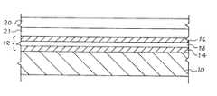
- FIG. 1shows a cross-section of a portion of a semiconductor structure substrate 10 .
- An ONO layer 12is on the semiconductor substrate 10 and includes a first oxide layer 14 , a second oxide layer 16 and a silicon nitride layer 18 between the first oxide layer and second oxide layer.
- a hard mask 21is on the ONO layer.
- the hard maskmay be made of tungsten, titanium, titanium nitride, silicon nitride, or silicon oxynitride.
- a photo resist layer 20is on the hard mask layer 21 .
- the photo resist layermay be any type of resist, including optical photoresist responsive to physical and near UV light, deep UV resist, etc. Alternatively, the photo resist layer may be an inorganic resist layer or an X-ray resist layer.
- Photo resist layer 20is next exposed to radiation of the appropriate wavelength and developed to form a resist pattern 22 on the ONO layer 12 , as illustrated in FIG. 2 .
- the resist patternexposes selected regions 24 of ONO layer 12 .
- portions of the ONO layer exposed through the resist patternare completely etched.
- the ONO layeris anisotropically etched, so that the ONO layer and the resist pattern have continuous, substantially vertical, sidewalls.
- the photo resist layer 22is then stripped and a stable oxide layer 40 is epitaxially re-grown on the exposed regions 24 of semiconductor substrate 10 .
- the re-grown stable oxide layer 40is of consistent thickness since the epitaxially re-growing process can be controlled much more accurately compared to the etching process.
- a doping processis then carried out over exposed selected regions 24 to form doped regions, as illustrated in FIG. 5 .
- an n-type region 19 and p-type pocket regions 23are formed.
- the doping processmay be carried out before or after the ONO etch.
- the n-type region and the p-type pocket regionsare formed after the ONO etch.
- P-type pocket regions 23are formed by doping semiconductor substrate 10 with a p-type dopant.
- semiconductor substrate 10is doped with a p-type dopant by ion implantation of boron.
- the ion implantationis preferably an angled implant, that is, an implant at an angle acute with respect to the principal surface 30 of semiconductor substrate 10 .
- the angled implant processcan be carried out at an angle of incidence of about 20 degrees to about 45 degrees depending upon the thickness and spacing of hard mask layer 21 .
- N-type region 19is formed by ion implantation of an n-type dopant, such as arsenic, antimony, phosphorus, and the like.
- the semiconductor substrate 10can be doped using molecular beam ion implantation or plasma assisted ion implantation.
- the ion implantationis preferably a direct ion implant performed at an angle substantially normal to principal surface 30 of semiconductor substrate 10 .
- bit-line oxide layer 44is formed.
- the bit-line oxide layeris formed by thermal oxidation of semiconductor substrate 10 using hard mask layer 21 as an oxidation mask.
- the ONO layerhaving been previously patterned, exposes selected regions 24 of semiconductor substrate 10 .
- the patterned portions of the ONO layerprevent the oxidation of the semiconductor substrate in the region underlying the ONO layer. Accordingly, the bit-line oxide layer is confined to the selected regions of the semiconductor substrate.
- the bit-line oxide layeris on bit-line region 32 in the semiconductor substrate, as illustrated in FIG. 6 .
- the term “regions”maybe one continuous region across the semiconductor substrate or multiple regions.
- the resulting bit-line oxide layer 44is of a consistent thickness and allows for a uniform amount of electrical charge to be carried between and across the semiconductor device.
- the hard mask layer 21is removed.
- the hard mask layer 21may be removed using a dry-etch process or a wet-etch solution, which are commonly known in the art.
- a wet-etch solutioncomprises hydrogen peroxide and other acid.
- the structure of the present inventionmay be incorporated into a semiconductor device such as an integrated circuit, for example a memory cell such as an SRAM, a DRAM, an EPROM, an EEPROM etc.; a programmable logic device; a data communications device; a clock generation device; electronic devices using semiconductors, automobiles, computers, and the like.
- a semiconductor devicesuch as an integrated circuit, for example a memory cell such as an SRAM, a DRAM, an EPROM, an EEPROM etc.; a programmable logic device; a data communications device; a clock generation device; electronic devices using semiconductors, automobiles, computers, and the like.
Landscapes
- Engineering & Computer Science (AREA)
- Physics & Mathematics (AREA)
- Condensed Matter Physics & Semiconductors (AREA)
- General Physics & Mathematics (AREA)
- Manufacturing & Machinery (AREA)
- Computer Hardware Design (AREA)
- Microelectronics & Electronic Packaging (AREA)
- Power Engineering (AREA)
- Semiconductor Memories (AREA)
- Non-Volatile Memory (AREA)
Abstract
Description
Claims (16)
Priority Applications (1)
| Application Number | Priority Date | Filing Date | Title |
|---|---|---|---|
| US09/798,667US6528390B2 (en) | 2001-03-02 | 2001-03-02 | Process for fabricating a non-volatile memory device |
Applications Claiming Priority (1)
| Application Number | Priority Date | Filing Date | Title |
|---|---|---|---|
| US09/798,667US6528390B2 (en) | 2001-03-02 | 2001-03-02 | Process for fabricating a non-volatile memory device |
Publications (2)
| Publication Number | Publication Date |
|---|---|
| US20020132446A1 US20020132446A1 (en) | 2002-09-19 |
| US6528390B2true US6528390B2 (en) | 2003-03-04 |
Family
ID=25173982
Family Applications (1)
| Application Number | Title | Priority Date | Filing Date |
|---|---|---|---|
| US09/798,667Expired - LifetimeUS6528390B2 (en) | 2001-03-02 | 2001-03-02 | Process for fabricating a non-volatile memory device |
Country Status (1)
| Country | Link |
|---|---|
| US (1) | US6528390B2 (en) |
Cited By (33)
| Publication number | Priority date | Publication date | Assignee | Title |
|---|---|---|---|---|
| US20030039153A1 (en)* | 2001-01-18 | 2003-02-27 | Eduardo Maayan | EEPROM array and method for operation thereof |
| US20040110315A1 (en)* | 2002-12-06 | 2004-06-10 | Matsushita Electric Industrial Co., Ltd. | Apparatus for evaluating amount of charge, method for fabricating the same, and method for evaluating amount of charge |
| US20050111257A1 (en)* | 1997-08-01 | 2005-05-26 | Boaz Eitan | Two bit non-volatile electrically erasable and programmable semiconductor memory cell utilizing asymmetrical charge trapping |
| US20060035435A1 (en)* | 2004-08-11 | 2006-02-16 | Renesas Technology, Corp. | Semiconductor device and manufacturing method for semiconductor device to reduce the lithography masks |
| US20060068551A1 (en)* | 2004-09-27 | 2006-03-30 | Saifun Semiconductors, Ltd. | Method for embedding NROM |
| US20070087503A1 (en)* | 2005-10-17 | 2007-04-19 | Saifun Semiconductors, Ltd. | Improving NROM device characteristics using adjusted gate work function |
| US7221138B2 (en) | 2005-09-27 | 2007-05-22 | Saifun Semiconductors Ltd | Method and apparatus for measuring charge pump output current |
| US7317633B2 (en) | 2004-07-06 | 2008-01-08 | Saifun Semiconductors Ltd | Protection of NROM devices from charge damage |
| US7352627B2 (en) | 2006-01-03 | 2008-04-01 | Saifon Semiconductors Ltd. | Method, system, and circuit for operating a non-volatile memory array |
| US7369440B2 (en) | 2005-01-19 | 2008-05-06 | Saifun Semiconductors Ltd. | Method, circuit and systems for erasing one or more non-volatile memory cells |
| US7420848B2 (en) | 2002-01-31 | 2008-09-02 | Saifun Semiconductors Ltd. | Method, system, and circuit for operating a non-volatile memory array |
| US7457183B2 (en) | 2003-09-16 | 2008-11-25 | Saifun Semiconductors Ltd. | Operating array cells with matched reference cells |
| US7466594B2 (en) | 2004-08-12 | 2008-12-16 | Saifun Semiconductors Ltd. | Dynamic matching of signal path and reference path for sensing |
| US7512009B2 (en) | 2001-04-05 | 2009-03-31 | Saifun Semiconductors Ltd. | Method for programming a reference cell |
| US7532529B2 (en) | 2004-03-29 | 2009-05-12 | Saifun Semiconductors Ltd. | Apparatus and methods for multi-level sensing in a memory array |
| US7535765B2 (en) | 2004-12-09 | 2009-05-19 | Saifun Semiconductors Ltd. | Non-volatile memory device and method for reading cells |
| US7605579B2 (en) | 2006-09-18 | 2009-10-20 | Saifun Semiconductors Ltd. | Measuring and controlling current consumption and output current of charge pumps |
| US7638835B2 (en) | 2006-02-28 | 2009-12-29 | Saifun Semiconductors Ltd. | Double density NROM with nitride strips (DDNS) |
| US7638850B2 (en) | 2004-10-14 | 2009-12-29 | Saifun Semiconductors Ltd. | Non-volatile memory structure and method of fabrication |
| US7668017B2 (en) | 2005-08-17 | 2010-02-23 | Saifun Semiconductors Ltd. | Method of erasing non-volatile memory cells |
| US7675782B2 (en) | 2002-10-29 | 2010-03-09 | Saifun Semiconductors Ltd. | Method, system and circuit for programming a non-volatile memory array |
| US7692961B2 (en) | 2006-02-21 | 2010-04-06 | Saifun Semiconductors Ltd. | Method, circuit and device for disturb-control of programming nonvolatile memory cells by hot-hole injection (HHI) and by channel hot-electron (CHE) injection |
| US7701779B2 (en) | 2006-04-27 | 2010-04-20 | Sajfun Semiconductors Ltd. | Method for programming a reference cell |
| US7738304B2 (en) | 2002-07-10 | 2010-06-15 | Saifun Semiconductors Ltd. | Multiple use memory chip |
| US7743230B2 (en) | 2003-01-31 | 2010-06-22 | Saifun Semiconductors Ltd. | Memory array programming circuit and a method for using the circuit |
| US7760554B2 (en) | 2006-02-21 | 2010-07-20 | Saifun Semiconductors Ltd. | NROM non-volatile memory and mode of operation |
| US7786512B2 (en) | 2005-07-18 | 2010-08-31 | Saifun Semiconductors Ltd. | Dense non-volatile memory array and method of fabrication |
| US7808818B2 (en) | 2006-01-12 | 2010-10-05 | Saifun Semiconductors Ltd. | Secondary injection for NROM |
| US20110177664A1 (en)* | 2010-01-20 | 2011-07-21 | Ping-Chia Shih | Mehtod for fabricating a sonos memory |
| US8053812B2 (en) | 2005-03-17 | 2011-11-08 | Spansion Israel Ltd | Contact in planar NROM technology |
| US8253452B2 (en) | 2006-02-21 | 2012-08-28 | Spansion Israel Ltd | Circuit and method for powering up an integrated circuit and an integrated circuit utilizing same |
| TWI469267B (en)* | 2010-01-21 | 2015-01-11 | United Microelectronics Corp | Method for fabricating a sonos memory |
| US20160079308A1 (en)* | 2014-09-11 | 2016-03-17 | Yuichi Ito | Semiconductor memory device and manufacturing method thereof |
Families Citing this family (2)
| Publication number | Priority date | Publication date | Assignee | Title |
|---|---|---|---|---|
| US6927472B2 (en)* | 2001-11-14 | 2005-08-09 | International Business Machines Corporation | Fuse structure and method to form the same |
| JP2018049976A (en)* | 2016-09-23 | 2018-03-29 | 東芝メモリ株式会社 | Manufacturing method of semiconductor device |
Citations (7)
| Publication number | Priority date | Publication date | Assignee | Title |
|---|---|---|---|---|
| US6093622A (en)* | 1997-09-08 | 2000-07-25 | Samsung Electronics, Co., Ltd. | Isolation method of semiconductor device using second pad oxide layer formed through chemical vapor deposition (CVD) |
| US6287917B1 (en)* | 1999-09-08 | 2001-09-11 | Advanced Micro Devices, Inc. | Process for fabricating an MNOS flash memory device |
| US6348711B1 (en)* | 1998-05-20 | 2002-02-19 | Saifun Semiconductors Ltd. | NROM cell with self-aligned programming and erasure areas |
| US6358761B1 (en)* | 1999-09-15 | 2002-03-19 | Taiwan Semiconductor Manufacturing Company | Silicon monitor for detection of H2O2 in acid bath |
| US6362052B1 (en)* | 2000-03-16 | 2002-03-26 | Advanced Micro Devices, Inc. | Use of an etch to reduce the thickness and around the edges of a resist mask during the creation of a memory cell |
| US6387754B2 (en)* | 2000-01-18 | 2002-05-14 | International Business Machines Corporation | Method of forming an on-chip decoupling capacitor with bottom hardmask |
| US6387752B1 (en)* | 1998-06-12 | 2002-05-14 | Nec Corporation | Semiconductor memory device and method of fabricating the same |
- 2001
- 2001-03-02USUS09/798,667patent/US6528390B2/ennot_activeExpired - Lifetime
Patent Citations (7)
| Publication number | Priority date | Publication date | Assignee | Title |
|---|---|---|---|---|
| US6093622A (en)* | 1997-09-08 | 2000-07-25 | Samsung Electronics, Co., Ltd. | Isolation method of semiconductor device using second pad oxide layer formed through chemical vapor deposition (CVD) |
| US6348711B1 (en)* | 1998-05-20 | 2002-02-19 | Saifun Semiconductors Ltd. | NROM cell with self-aligned programming and erasure areas |
| US6387752B1 (en)* | 1998-06-12 | 2002-05-14 | Nec Corporation | Semiconductor memory device and method of fabricating the same |
| US6287917B1 (en)* | 1999-09-08 | 2001-09-11 | Advanced Micro Devices, Inc. | Process for fabricating an MNOS flash memory device |
| US6358761B1 (en)* | 1999-09-15 | 2002-03-19 | Taiwan Semiconductor Manufacturing Company | Silicon monitor for detection of H2O2 in acid bath |
| US6387754B2 (en)* | 2000-01-18 | 2002-05-14 | International Business Machines Corporation | Method of forming an on-chip decoupling capacitor with bottom hardmask |
| US6362052B1 (en)* | 2000-03-16 | 2002-03-26 | Advanced Micro Devices, Inc. | Use of an etch to reduce the thickness and around the edges of a resist mask during the creation of a memory cell |
Cited By (44)
| Publication number | Priority date | Publication date | Assignee | Title |
|---|---|---|---|---|
| US20050111257A1 (en)* | 1997-08-01 | 2005-05-26 | Boaz Eitan | Two bit non-volatile electrically erasable and programmable semiconductor memory cell utilizing asymmetrical charge trapping |
| US7405969B2 (en) | 1997-08-01 | 2008-07-29 | Saifun Semiconductors Ltd. | Non-volatile memory cell and non-volatile memory devices |
| US7116577B2 (en) | 1997-08-01 | 2006-10-03 | Saifun Semiconductors Ltd | Two bit non-volatile electrically erasable and programmable semiconductor memory cell utilizing asymmetrical charge trapping |
| US20060262598A1 (en)* | 1997-08-01 | 2006-11-23 | Saifun Semiconductors Ltd. | Two bit non-volatile electrically erasable and programmable semiconductor memory cell utilizing asymmetrical charge trapping |
| US20030039153A1 (en)* | 2001-01-18 | 2003-02-27 | Eduardo Maayan | EEPROM array and method for operation thereof |
| US7518908B2 (en) | 2001-01-18 | 2009-04-14 | Saifun Semiconductors Ltd. | EEPROM array and method for operation thereof |
| US7512009B2 (en) | 2001-04-05 | 2009-03-31 | Saifun Semiconductors Ltd. | Method for programming a reference cell |
| US7420848B2 (en) | 2002-01-31 | 2008-09-02 | Saifun Semiconductors Ltd. | Method, system, and circuit for operating a non-volatile memory array |
| US7738304B2 (en) | 2002-07-10 | 2010-06-15 | Saifun Semiconductors Ltd. | Multiple use memory chip |
| US7675782B2 (en) | 2002-10-29 | 2010-03-09 | Saifun Semiconductors Ltd. | Method, system and circuit for programming a non-volatile memory array |
| US20050263833A1 (en)* | 2002-12-06 | 2005-12-01 | Matsushita Electric Industrial Co., Ltd. | Apparatus for evaluating amount of charge, method for fabricating the same, and method for evaluating amount of charge |
| US6946305B2 (en)* | 2002-12-06 | 2005-09-20 | Matsushita Electric Industrial Co., Ltd. | Apparatus for evaluating amount of charge, method for fabricating the same, and method for evaluating amount of charge |
| US20040110315A1 (en)* | 2002-12-06 | 2004-06-10 | Matsushita Electric Industrial Co., Ltd. | Apparatus for evaluating amount of charge, method for fabricating the same, and method for evaluating amount of charge |
| US7743230B2 (en) | 2003-01-31 | 2010-06-22 | Saifun Semiconductors Ltd. | Memory array programming circuit and a method for using the circuit |
| US7457183B2 (en) | 2003-09-16 | 2008-11-25 | Saifun Semiconductors Ltd. | Operating array cells with matched reference cells |
| US7532529B2 (en) | 2004-03-29 | 2009-05-12 | Saifun Semiconductors Ltd. | Apparatus and methods for multi-level sensing in a memory array |
| US7317633B2 (en) | 2004-07-06 | 2008-01-08 | Saifun Semiconductors Ltd | Protection of NROM devices from charge damage |
| US20060035435A1 (en)* | 2004-08-11 | 2006-02-16 | Renesas Technology, Corp. | Semiconductor device and manufacturing method for semiconductor device to reduce the lithography masks |
| US7863131B2 (en)* | 2004-08-11 | 2011-01-04 | Renesas Electronics Corporation | Semiconductor device and manufacturing method for semiconductor device to reduce the lithography masks |
| US7466594B2 (en) | 2004-08-12 | 2008-12-16 | Saifun Semiconductors Ltd. | Dynamic matching of signal path and reference path for sensing |
| US20060068551A1 (en)* | 2004-09-27 | 2006-03-30 | Saifun Semiconductors, Ltd. | Method for embedding NROM |
| US7964459B2 (en) | 2004-10-14 | 2011-06-21 | Spansion Israel Ltd. | Non-volatile memory structure and method of fabrication |
| US7638850B2 (en) | 2004-10-14 | 2009-12-29 | Saifun Semiconductors Ltd. | Non-volatile memory structure and method of fabrication |
| US7535765B2 (en) | 2004-12-09 | 2009-05-19 | Saifun Semiconductors Ltd. | Non-volatile memory device and method for reading cells |
| US7468926B2 (en) | 2005-01-19 | 2008-12-23 | Saifun Semiconductors Ltd. | Partial erase verify |
| US7369440B2 (en) | 2005-01-19 | 2008-05-06 | Saifun Semiconductors Ltd. | Method, circuit and systems for erasing one or more non-volatile memory cells |
| US8053812B2 (en) | 2005-03-17 | 2011-11-08 | Spansion Israel Ltd | Contact in planar NROM technology |
| US7786512B2 (en) | 2005-07-18 | 2010-08-31 | Saifun Semiconductors Ltd. | Dense non-volatile memory array and method of fabrication |
| US7668017B2 (en) | 2005-08-17 | 2010-02-23 | Saifun Semiconductors Ltd. | Method of erasing non-volatile memory cells |
| US7221138B2 (en) | 2005-09-27 | 2007-05-22 | Saifun Semiconductors Ltd | Method and apparatus for measuring charge pump output current |
| US20070087503A1 (en)* | 2005-10-17 | 2007-04-19 | Saifun Semiconductors, Ltd. | Improving NROM device characteristics using adjusted gate work function |
| US7352627B2 (en) | 2006-01-03 | 2008-04-01 | Saifon Semiconductors Ltd. | Method, system, and circuit for operating a non-volatile memory array |
| US7808818B2 (en) | 2006-01-12 | 2010-10-05 | Saifun Semiconductors Ltd. | Secondary injection for NROM |
| US8253452B2 (en) | 2006-02-21 | 2012-08-28 | Spansion Israel Ltd | Circuit and method for powering up an integrated circuit and an integrated circuit utilizing same |
| US7760554B2 (en) | 2006-02-21 | 2010-07-20 | Saifun Semiconductors Ltd. | NROM non-volatile memory and mode of operation |
| US7692961B2 (en) | 2006-02-21 | 2010-04-06 | Saifun Semiconductors Ltd. | Method, circuit and device for disturb-control of programming nonvolatile memory cells by hot-hole injection (HHI) and by channel hot-electron (CHE) injection |
| US7638835B2 (en) | 2006-02-28 | 2009-12-29 | Saifun Semiconductors Ltd. | Double density NROM with nitride strips (DDNS) |
| US7701779B2 (en) | 2006-04-27 | 2010-04-20 | Sajfun Semiconductors Ltd. | Method for programming a reference cell |
| US7605579B2 (en) | 2006-09-18 | 2009-10-20 | Saifun Semiconductors Ltd. | Measuring and controlling current consumption and output current of charge pumps |
| US20110177664A1 (en)* | 2010-01-20 | 2011-07-21 | Ping-Chia Shih | Mehtod for fabricating a sonos memory |
| US8633079B2 (en)* | 2010-01-20 | 2014-01-21 | United Microelectronics Corp. | Method for fabricating a SONOS memory |
| TWI469267B (en)* | 2010-01-21 | 2015-01-11 | United Microelectronics Corp | Method for fabricating a sonos memory |
| US20160079308A1 (en)* | 2014-09-11 | 2016-03-17 | Yuichi Ito | Semiconductor memory device and manufacturing method thereof |
| US9698342B2 (en)* | 2014-09-11 | 2017-07-04 | Kabushiki Kaisha Toshiba | Contact layer for magnetic tunnel junction element and manufacturing method thereof |
Also Published As
| Publication number | Publication date |
|---|---|
| US20020132446A1 (en) | 2002-09-19 |
Similar Documents
| Publication | Publication Date | Title |
|---|---|---|
| US6528390B2 (en) | Process for fabricating a non-volatile memory device | |
| US6562683B1 (en) | Bit-line oxidation by removing ONO oxide prior to bit-line implant | |
| US6642148B1 (en) | RELACS shrink method applied for single print resist mask for LDD or buried bitline implants using chemically amplified DUV type photoresist | |
| US6410388B1 (en) | Process for optimizing pocket implant profile by RTA implant annealing for a non-volatile semiconductor device | |
| US6034403A (en) | High density flat cell mask ROM | |
| US6605506B2 (en) | Method of fabricating a scalable stacked-gate flash memory device and its high-density memory arrays | |
| US7256091B2 (en) | Method of manufacturing a semiconductor device with a self-aligned polysilicon electrode | |
| US20100048015A1 (en) | Methods of Forming Void-Free Layers in Openings of Semiconductor Substrates | |
| US6248635B1 (en) | Process for fabricating a bit-line in a monos device using a dual layer hard mask | |
| US5460991A (en) | Method of making high coupling ratio flash EEPROM device | |
| US6905927B2 (en) | Method for forming a gate electrode in a semiconductor device including re-oxidation for restraining the thickness of the gate oxide | |
| US6048765A (en) | Method of forming high density buried bit line flash EEPROM memory cell with a shallow trench floating gate | |
| US6495420B2 (en) | Method of making a single transistor non-volatile memory device | |
| US6008087A (en) | Method to form high density NAND structure nonvolatile memories | |
| US7871885B2 (en) | Manufacturing method of flash memory device | |
| US6057195A (en) | Method of fabricating high density flat cell mask ROM | |
| US6436778B1 (en) | Re-oxidation approach to improve peripheral gate oxide integrity in a tunnel nitride oxidation process | |
| US6372580B1 (en) | Process for making mask ROM using a salicide process and mask ROM | |
| US6168993B1 (en) | Process for fabricating a semiconductor device having a graded junction | |
| US6255167B1 (en) | Method of forming high density buried bit line flash EEPROM memory cell with a shallow trench floating gate | |
| US20090101963A1 (en) | Split charge storage node inner spacer process | |
| US6277693B1 (en) | Self-aligned process for forming source line of ETOX flash memory | |
| CN1328763C (en) | Semiconductor structure with partially etched gate and method of making same | |
| US6417048B1 (en) | Method for fabricating flash memory with recessed floating gates | |
| US6486029B1 (en) | Integration of an ion implant hard mask structure into a process for fabricating high density memory cells |
Legal Events
| Date | Code | Title | Description |
|---|---|---|---|
| AS | Assignment | Owner name:ADVANCED MICRO DEVICES, CALIFORNIA Free format text:ASSIGNMENT OF ASSIGNORS INTEREST;ASSIGNORS:KOMORI, HIDEKI;FOOTE, DAVID K.;WANG, FEI;AND OTHERS;REEL/FRAME:011597/0061 Effective date:20010215 | |
| AS | Assignment | Owner name:ADVANCED MICRO DEVICES, INC., CALIFORNIA Free format text:CORRECTIVE DOCUMENT;ASSIGNORS:KOMORI, HIDEKI;FOOTE, DAVID K.;WANG, FEI;AND OTHERS;REEL/FRAME:012171/0510;SIGNING DATES FROM 20010122 TO 20010215 Owner name:FUJITSU LIMITED, JAPAN Free format text:CORRECTIVE DOCUMENT;ASSIGNORS:KOMORI, HIDEKI;FOOTE, DAVID K.;WANG, FEI;AND OTHERS;REEL/FRAME:012171/0510;SIGNING DATES FROM 20010122 TO 20010215 | |
| STCF | Information on status: patent grant | Free format text:PATENTED CASE | |
| AS | Assignment | Owner name:AMD (U.S.) HOLDINGS, INC., CALIFORNIA Free format text:ASSIGNMENT OF ASSIGNORS INTEREST;ASSIGNOR:ADVANCED MICRO DEVICES, INC.;REEL/FRAME:014782/0080 Effective date:20040515 | |
| AS | Assignment | Owner name:AMD INVESTMENTS, INC., CALIFORNIA Free format text:ASSIGNMENT OF ASSIGNORS INTEREST;ASSIGNOR:AMD (U.S.) HOLDINGS, INC.;REEL/FRAME:014782/0971 Effective date:20040515 | |
| AS | Assignment | Owner name:FASL LLC, CALIFORNIA Free format text:ASSIGNMENT OF ASSIGNORS INTEREST;ASSIGNORS:AMD INVESTMENTS, INC.;FIJITSU LIMITED;REEL/FRAME:014822/0098;SIGNING DATES FROM 20040515 TO 20040525 | |
| FPAY | Fee payment | Year of fee payment:4 | |
| AS | Assignment | Owner name:SPANSION LLC,CALIFORNIA Free format text:CHANGE OF NAME;ASSIGNOR:FASL LLC;REEL/FRAME:024170/0300 Effective date:20100401 | |
| AS | Assignment | Owner name:BARCLAYS BANK PLC,NEW YORK Free format text:SECURITY AGREEMENT;ASSIGNORS:SPANSION LLC;SPANSION INC.;SPANSION TECHNOLOGY INC.;AND OTHERS;REEL/FRAME:024522/0338 Effective date:20100510 Owner name:BARCLAYS BANK PLC, NEW YORK Free format text:SECURITY AGREEMENT;ASSIGNORS:SPANSION LLC;SPANSION INC.;SPANSION TECHNOLOGY INC.;AND OTHERS;REEL/FRAME:024522/0338 Effective date:20100510 | |
| FPAY | Fee payment | Year of fee payment:8 | |
| FPAY | Fee payment | Year of fee payment:12 | |
| AS | Assignment | Owner name:SPANSION INC., CALIFORNIA Free format text:RELEASE BY SECURED PARTY;ASSIGNOR:BARCLAYS BANK PLC;REEL/FRAME:035201/0159 Effective date:20150312 Owner name:SPANSION LLC, CALIFORNIA Free format text:RELEASE BY SECURED PARTY;ASSIGNOR:BARCLAYS BANK PLC;REEL/FRAME:035201/0159 Effective date:20150312 Owner name:SPANSION TECHNOLOGY LLC, CALIFORNIA Free format text:RELEASE BY SECURED PARTY;ASSIGNOR:BARCLAYS BANK PLC;REEL/FRAME:035201/0159 Effective date:20150312 | |
| AS | Assignment | Owner name:MORGAN STANLEY SENIOR FUNDING, INC., NEW YORK Free format text:SECURITY INTEREST;ASSIGNORS:CYPRESS SEMICONDUCTOR CORPORATION;SPANSION LLC;REEL/FRAME:035240/0429 Effective date:20150312 | |
| AS | Assignment | Owner name:CYPRESS SEMICONDUCTOR CORPORATION, CALIFORNIA Free format text:ASSIGNMENT OF ASSIGNORS INTEREST;ASSIGNOR:SPANSION, LLC;REEL/FRAME:036025/0453 Effective date:20150601 | |
| AS | Assignment | Owner name:MONTEREY RESEARCH, LLC, CALIFORNIA Free format text:ASSIGNMENT OF ASSIGNORS INTEREST;ASSIGNOR:CYPRESS SEMICONDUCTOR CORPORATION;REEL/FRAME:049717/0618 Effective date:20190628 | |
| AS | Assignment | Owner name:CYPRESS SEMICONDUCTOR CORPORATION, CALIFORNIA Free format text:RELEASE BY SECURED PARTY;ASSIGNOR:MORGAN STANLEY SENIOR FUNDING INC.,;REEL/FRAME:049989/0248 Effective date:20190628 | |
| AS | Assignment | Owner name:MORGAN STANLEY SENIOR FUNDING, INC., NEW YORK Free format text:CORRECTIVE ASSIGNMENT TO CORRECT THE 8647899 PREVIOUSLY RECORDED ON REEL 035240 FRAME 0429. ASSIGNOR(S) HEREBY CONFIRMS THE SECURITY INTERST;ASSIGNORS:CYPRESS SEMICONDUCTOR CORPORATION;SPANSION LLC;REEL/FRAME:058002/0470 Effective date:20150312 |