US6526996B1 - Dry clean method instead of traditional wet clean after metal etch - Google Patents
Dry clean method instead of traditional wet clean after metal etchDownload PDFInfo
- Publication number
- US6526996B1 US6526996B1US09/591,848US59184800AUS6526996B1US 6526996 B1US6526996 B1US 6526996B1US 59184800 AUS59184800 AUS 59184800AUS 6526996 B1US6526996 B1US 6526996B1
- Authority
- US
- United States
- Prior art keywords
- containing gas
- metallization structure
- etched metallization
- magnetic field
- predetermined time
- Prior art date
- Legal status (The legal status is an assumption and is not a legal conclusion. Google has not performed a legal analysis and makes no representation as to the accuracy of the status listed.)
- Expired - Lifetime, expires
Links
Images


Classifications
- H—ELECTRICITY
- H01—ELECTRIC ELEMENTS
- H01L—SEMICONDUCTOR DEVICES NOT COVERED BY CLASS H10
- H01L21/00—Processes or apparatus adapted for the manufacture or treatment of semiconductor or solid state devices or of parts thereof
- H01L21/02—Manufacture or treatment of semiconductor devices or of parts thereof
- H01L21/02041—Cleaning
- H01L21/02057—Cleaning during device manufacture
- H01L21/02068—Cleaning during device manufacture during, before or after processing of conductive layers, e.g. polysilicon or amorphous silicon layers
- H01L21/02071—Cleaning during device manufacture during, before or after processing of conductive layers, e.g. polysilicon or amorphous silicon layers the processing being a delineation, e.g. RIE, of conductive layers
- H—ELECTRICITY
- H01—ELECTRIC ELEMENTS
- H01L—SEMICONDUCTOR DEVICES NOT COVERED BY CLASS H10
- H01L21/00—Processes or apparatus adapted for the manufacture or treatment of semiconductor or solid state devices or of parts thereof
- H01L21/02—Manufacture or treatment of semiconductor devices or of parts thereof
- H01L21/04—Manufacture or treatment of semiconductor devices or of parts thereof the devices having potential barriers, e.g. a PN junction, depletion layer or carrier concentration layer
- H01L21/18—Manufacture or treatment of semiconductor devices or of parts thereof the devices having potential barriers, e.g. a PN junction, depletion layer or carrier concentration layer the devices having semiconductor bodies comprising elements of Group IV of the Periodic Table or AIIIBV compounds with or without impurities, e.g. doping materials
- H01L21/30—Treatment of semiconductor bodies using processes or apparatus not provided for in groups H01L21/20 - H01L21/26
- H01L21/31—Treatment of semiconductor bodies using processes or apparatus not provided for in groups H01L21/20 - H01L21/26 to form insulating layers thereon, e.g. for masking or by using photolithographic techniques; After treatment of these layers; Selection of materials for these layers
- H01L21/3205—Deposition of non-insulating-, e.g. conductive- or resistive-, layers on insulating layers; After-treatment of these layers
- H01L21/321—After treatment
- H01L21/3213—Physical or chemical etching of the layers, e.g. to produce a patterned layer from a pre-deposited extensive layer
- H01L21/32133—Physical or chemical etching of the layers, e.g. to produce a patterned layer from a pre-deposited extensive layer by chemical means only
- H01L21/32135—Physical or chemical etching of the layers, e.g. to produce a patterned layer from a pre-deposited extensive layer by chemical means only by vapour etching only
- H01L21/32136—Physical or chemical etching of the layers, e.g. to produce a patterned layer from a pre-deposited extensive layer by chemical means only by vapour etching only using plasmas
- Y—GENERAL TAGGING OF NEW TECHNOLOGICAL DEVELOPMENTS; GENERAL TAGGING OF CROSS-SECTIONAL TECHNOLOGIES SPANNING OVER SEVERAL SECTIONS OF THE IPC; TECHNICAL SUBJECTS COVERED BY FORMER USPC CROSS-REFERENCE ART COLLECTIONS [XRACs] AND DIGESTS
- Y10—TECHNICAL SUBJECTS COVERED BY FORMER USPC
- Y10S—TECHNICAL SUBJECTS COVERED BY FORMER USPC CROSS-REFERENCE ART COLLECTIONS [XRACs] AND DIGESTS
- Y10S134/00—Cleaning and liquid contact with solids
- Y10S134/902—Semiconductor wafer
- Y—GENERAL TAGGING OF NEW TECHNOLOGICAL DEVELOPMENTS; GENERAL TAGGING OF CROSS-SECTIONAL TECHNOLOGIES SPANNING OVER SEVERAL SECTIONS OF THE IPC; TECHNICAL SUBJECTS COVERED BY FORMER USPC CROSS-REFERENCE ART COLLECTIONS [XRACs] AND DIGESTS
- Y10—TECHNICAL SUBJECTS COVERED BY FORMER USPC
- Y10S—TECHNICAL SUBJECTS COVERED BY FORMER USPC CROSS-REFERENCE ART COLLECTIONS [XRACs] AND DIGESTS
- Y10S438/00—Semiconductor device manufacturing: process
- Y10S438/906—Cleaning of wafer as interim step
Definitions
- the present inventionrelates generally to methods of forming metal structures in semiconductor devices and specifically to methods of using a dry cleaning method instead of a traditional wet clean method after metal etch.
- wet cleaning methodscan leave chlorine (Cl 2 ) trapped in a thin sidewall polymer which maximizes corrosion and pitting of, for example, an aluminum (Al) or aluminum alloy substrate. If a thicker sidewall polymer is formed to minimize the exposure of the aluminum/aluminum alloy substrate to Cl 2 , the difficulty of a more narrow window within which to perform the wet clean arises.
- passivationformation of the sidewall polymer within the etched structure
- passivation stepformation of the sidewall polymer within the etched structure
- an adequate passivation step followed by a poor clean stepwill also cause pitting and corrosion.
- device dimensions, or design rulegetting smaller and smaller, the influence of any such defects on device performance and reliability is becoming greater and greater.
- a further problemis the ring type residue, or when a high Rc occurs at the wafer edge due to penetration of TiN from an ACT wet clean.
- metal corrosioncan occur that is caused by the reaction of chlorine gas and humidity to form HCl acid.
- U.S. Pat. No. 4,501,061 to Wonnacott et al.describes a method for stripping an organic photoresist layer from a semiconductor device using CF 4 and O 2 plasma.
- the photoresist layeris oxidized with oxygen plasma and residual sulfur species are subsequently removed using a fluorine-containing plasma.
- U.S. Pat. No. 5,378,653 to Yanagidadescribes a method of forming an Al-based pattern whereby dry etching with high selectively of an Al-based metallization layer and effective preventive measures for after-corrosion can be realized. If after etching residual chlorine is removed by O 2 plasma ashing or plasma processing using a fluorine based gas, durability to after-corrosion can be improved further.
- U.S. Pat. No. 5,599,743 to Nakagawa et al.describes a method of manufacturing a semiconductor device that includes etching an aluminum or alloy film through a mask by chlorination and/or bromination with plasma. The film is exposed to either: a gas plasma not liable to deposit or oxidize, but capable of substituting fluoride for chloride and/or bromide; or a gas mixture plasma comprising hydrogen and the above mentioned gas. The device is then washed with water and the mask is removed.
- the ratio of etchants Cl 2 and HCl and an inert gas, such as N 2are controlled in a manner such that a very thin sidewall layer (10-100 ⁇ ) of reaction byproducts during RIE are deposited on the sidewalls of trenches within the etched metallization.
- the processdoes not use magnetic fields during etching.
- U.S. Pat. No. 5,908,319 to Xu et al.describes forming a microwave plasma in a microwave downstream process from a gas that has a small quantity of fluorine to enhance ashing without substantial oxide loss. This process may be performed before or after other microwave downstream processes or reactive ion etching processes.
- U.S. Pat. No. 5,795,831 to Nakayama et al.describes a method of removing a resist layer including a reactive ion etch (RIE) process and a downstream microwave process each performed at a wafer temperature no greater than about 60° C.
- RIEreactive ion etch
- the low temperatureprecludes having to pre-heat the resist to drive off solvents.
- U.S. Pat. No. 6,017,826 to Zhou et al.describes a method for forming a patterned layer within a microelectronics fabrication.
- a first plasma etch methodis used to etch a blanket hard mask using an overlying patterned photoresist layer as a first etch mask layer, while exposing a blanket chlorine containing plasma etchable layer.
- a second plasma etch methodis used to etch the exposed blanket chlorine containing plasma etchable layer using at least the patterned blanket hard mask layer as a second etch mask layer.
- the second plasma etch sidewall passivation layeris formed upon a sidewall of the patterned chlorine containing plasma etchable layer.
- a third plasma etch methodstrips the sidewall passivation layer while sequentially oxidizing the sidewall of the patterned chlorine containing plasma etchable layer.
- the third plasma etch methodemploys a third etchant gas composition which, upon plasma activation, forms an oxygen containing oxidizing species.
- U.S. Pat. No. 5,578,133 to Sugino et al.describes a dry cleaning process for removing metal contaminants from a surface of an oxide film.
- a reaction areais formed on the oxide film such that a silicon surface is formed corresponding to the reaction area.
- a dry cleaning gasis supplied to the oxide film including the reaction area to produce silicon halide molecules.
- the dry cleaning gasbeing selected from the group essentially consisting of chlorine, bromine, hydrogen chloride, hydrogen bromide, and a mixture thereof.
- the silicon halide molecules so formedare supplied to a surface of the oxide film and metal elements existing on the surface of the oxide film are removed.
- Another object of the present inventionis to provide an improved dry cleaning method after metal etch to lower the defect density and engineering repair time.
- an etched metallization structureis provided and placed in a processing chamber.
- the etched metallization structureis cleaned by introducing a fluorine containing gas/oxygen containing gas mixture into the processing chamber proximate the etched metallization structure without the use of a downstream microwave while applying a magnetic field proximate the etched metallization structure and maintaining a pressure of less than about 50 millitorr within the processing chamber for a predetermined time.
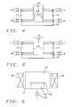
- FIGS. 1 through 5schematically illustrate in cross-sectional representation a preferred embodiment of the present invention.
- FIG. 6is a cross-sectional representation of the tool that may be used with the present invention.
- FIGS. 7A and 7Bare top down, plan views of the permissible magnet orientations.
- a conventional aluminum or aluminum alloy metallizationtypically is comprised of dielectric layer 30 (e.g. ILD, IMD, or oxide), bottom barrier layer 10 , bulk aluminum or aluminum alloy 12 , and upper barrier layer 14 .
- dielectric layer 30e.g. ILD, IMD, or oxide
- bottom barrier layer 10e.g., bottom barrier layer 10
- bulk aluminum or aluminum alloy 12e.g., bulk aluminum or aluminum alloy 12
- upper barrier layer 14e.g., aluminum or aluminum alloy
- Patterned photoresist layer 16overlies upper barrier layer 14 .
- Barrier layers 10 , 14are preferably comprised of an inner Ti layer 10 B, 14 B adjacent bulk aluminum or aluminum alloy 12 , and outer TiN layer 10 A, 14 A facing away from bulk aluminum or aluminum alloy 12 .
- Barrier layers 10 , 14may also be comprised of other metal or metal alloys such as tantalum, tungsten, molybdenum, chromium, vanadium, niobium, zirconium, or metal-silicon nitrides.
- Barrier layers 10 , 14are preferably from about 5 to 150 nm thick.
- Bulk aluminum or aluminum alloy 12is preferably an aluminum copper alloy with 0.5% copper (Al-0.5% Cu or just Al(Cu)).
- Al(Cu) layer 12is preferably from about 100 to 1500 nm thick.
- Photoresist layer 16may be comprised of a variety of organic materials, such as Barl 900TM material manufactured by Brewer Science, U.S.A., or Novalic material because they are photosensitive.
- the metallization etch processincludes the following parameters: from about 0 to 100 sccm BCl 3 gas flow, from about 0 to 200 sccm Cl 2 gas flow, from about 0 to 20 sccm N 2 gas flow, from about 0 to 20 sccm CH 4 gas flow, and from about 0 to 20 sccm CHF 3 .
- Either a Lam Research model TCP 9600 tool or an AMAT (Applied Materials) model DPS metal toolmay be used.
- barrier layer 10As shown in FIG. 3, as the metallization is etched through bottom barrier layer 10 (Ti layer 10 B/TiN layer 10 A), polymer layer 20 extends to the etched sidewalls of barrier layer 10 .
- Polymer layer 20serves to protect sidewalls 22 from the etchant and preserve the anisotropic nature of the etching, i.e. maintenance of vertical sidewalls 22 .
- the conventional metal stack for aluminum-0.5%copper alloy(Al(Cu)) is photoresist 16 /TiN layer 14 A/Ti layer 14 B/Al(Cu) layer 12 /Ti layer 10 B/TiN layer 10 A/oxide layer 30
- the property of the sidewall polymer 20 that forms over the sidewalls 22 of the etched structureis organic plus oxide-like.
- This polymer 20is quite a bit stickier on the metal line and sidewall 22 after plasma etching and in-situ photoresist (PR) 16 stripping.
- a strategyis therefore needed for a dry clean oxide (sidewall polymer 20 ) and PR 16 removal.
- Step I and Step IIThe inventors have discovered that removing the polymer layer 20 requires the use of a two step process (Step I and Step II):
- STEP Ilow pressure of less than 50 millitorr, more preferably from about 10 to 50 millitorr, and most preferably about 20 millitorr;
- medium RF powerof greater than about 200 W, more preferably from about 200 to 500 W, and most preferably about 300 W;
- a magnetic fieldgreater than about 10 gauss (G), more preferably from about 20 to 100 gauss, and most preferably about 20 gauss at a radio frequency of about 13.56 MHz;
- the fluorine containing gasmay be CF 4 , NF 3 , or CHF 3 , and is preferably CF 4
- the oxygen containing gasmay be O 2 , or O 3 , and is preferably O 2 .
- DIdeionized water
- initial treatment of the structure of FIG. 3leaves sidewall polymer residue 20 extending over outer TiN layer 14 A.
- FIG. 5further treating the structure of FIG. 4 in accordance with the present invention removes the polymer layer 20 from sidewalls 22 within trench 24 and from outer TiN layer 14 A.
- FIG. 6illustrates the major elements of the tool that may be used in the present invention.
- the wafer 60is supported by an electrode statistic chuck (ESC) 62 within processing chamber 64 .
- RF power source 66supplies the necessary RF power.
- Processing chamber 64is flanked by magnetic field 68 .
- FIGS. 7A and 7Billustrate top down, plan views of two permissible magnet 70 A, 70 B, 70 C, 70 D; and 72 A, 72 B, 72 C, and 72 D, respectively, orientations.
- Lam Research model TCP 9600 tooland the AMAT model DPS-metal tool.
- the following tool configurationsmay also be used: magnetic enhanced RIE and magnetic confinement triode RIE.
- Step 1Step 2
- Step 2One Step Platen Temp 30 30 40 30 15 (° C.) Pins Down Down 2 2 — (up/down) Pressure 700 700 450 350 20 (millitorr)
- Microwave 1400— 1500 — — Power RF/Platen — 200 150 225 300
- Power O 2 (sccm) 800— 980 — 40
- N 2 /H 2 (sccm)500 100 480 — NF 3 (sccm) — — 80 — — CF 4 200 50 — 20 10
- the yieldis increased due to the decreased defect density
- fluorine gasis useful for oxide removal (such as TiO x , AlO x , CuO x , and SiO 2 ), and an O 2 /N 2 gas mixture or an H 2 /N 2 gas mixture or both gas mixtures is useful for photoresist layer 16 removal/strip. So it would be anticipated that using fluorine gas with an O 2 /N 2 gas mixture or an H 2 /N 2 gas mixture or both gas mixtures would be useful to strip photoresist layer 16 and to remove sidewall polymer layer 20 .
Landscapes
- Engineering & Computer Science (AREA)
- Physics & Mathematics (AREA)
- Condensed Matter Physics & Semiconductors (AREA)
- General Physics & Mathematics (AREA)
- Manufacturing & Machinery (AREA)
- Computer Hardware Design (AREA)
- Microelectronics & Electronic Packaging (AREA)
- Power Engineering (AREA)
- Drying Of Semiconductors (AREA)
Abstract
Description
| Process | Dry Clean (A) | Dry Clean (B) | |
| Parameter | Step |
| 1 | One | ||||
| Platen Temp | |||||
| 30 | 30 | 40 | 30 | 15 | |
| (° C.) | |||||
| Pins | Down | Down | 2 | 2 | — |
| (up/down) | |||||
| 700 | 700 | 450 | 350 | 20 | |
| (millitorr) | |||||
| Microwave | 1400 | — | 1500 | — | — |
| Power | |||||
| RF/Platen | — | 200 | 150 | 225 | 300 |
| Power | |||||
| O2(sccm) | 800 | — | 980 | — | 40 |
| N2/H2(sccm) | — | 500 | 100 | 480 | — |
| NF3 (sccm) | — | — | 80 | — | — |
| CF4 | 200 | 50 | — | 20 | 10 |
| Magnetic (G) | — | — | — | — | 20 |
| 30 | 30 | 30 | 20 | 30 | |
| (sec) | |||||
Claims (20)
Priority Applications (2)
| Application Number | Priority Date | Filing Date | Title |
|---|---|---|---|
| US09/591,848US6526996B1 (en) | 2000-06-12 | 2000-06-12 | Dry clean method instead of traditional wet clean after metal etch |
| US10/339,157US20030104697A1 (en) | 2000-06-12 | 2003-01-09 | Dry clean method instead of traditional wet clean after metal etch |
Applications Claiming Priority (1)
| Application Number | Priority Date | Filing Date | Title |
|---|---|---|---|
| US09/591,848US6526996B1 (en) | 2000-06-12 | 2000-06-12 | Dry clean method instead of traditional wet clean after metal etch |
Related Child Applications (1)
| Application Number | Title | Priority Date | Filing Date |
|---|---|---|---|
| US10/339,157DivisionUS20030104697A1 (en) | 2000-06-12 | 2003-01-09 | Dry clean method instead of traditional wet clean after metal etch |
Publications (1)
| Publication Number | Publication Date |
|---|---|
| US6526996B1true US6526996B1 (en) | 2003-03-04 |
Family
ID=24368201
Family Applications (2)
| Application Number | Title | Priority Date | Filing Date |
|---|---|---|---|
| US09/591,848Expired - LifetimeUS6526996B1 (en) | 2000-06-12 | 2000-06-12 | Dry clean method instead of traditional wet clean after metal etch |
| US10/339,157AbandonedUS20030104697A1 (en) | 2000-06-12 | 2003-01-09 | Dry clean method instead of traditional wet clean after metal etch |
Family Applications After (1)
| Application Number | Title | Priority Date | Filing Date |
|---|---|---|---|
| US10/339,157AbandonedUS20030104697A1 (en) | 2000-06-12 | 2003-01-09 | Dry clean method instead of traditional wet clean after metal etch |
Country Status (1)
| Country | Link |
|---|---|
| US (2) | US6526996B1 (en) |
Cited By (34)
| Publication number | Priority date | Publication date | Assignee | Title |
|---|---|---|---|---|
| US20030173332A1 (en)* | 2002-03-18 | 2003-09-18 | Shinichi Hakamada | Method of forming electrode for saw device |
| US6796314B1 (en)* | 2001-09-07 | 2004-09-28 | Novellus Systems, Inc. | Using hydrogen gas in a post-etch radio frequency-plasma contact cleaning process |
| US6848454B2 (en)* | 2000-11-21 | 2005-02-01 | Sharp Kabushiki Kaisha | Method of manufacturing semiconductor device |
| US20050266692A1 (en)* | 2004-06-01 | 2005-12-01 | Brask Justin K | Method of patterning a film |
| US20050279380A1 (en)* | 2004-06-17 | 2005-12-22 | Uvtech Systems, Inc. | Method for surface cleaning |
| US20070090408A1 (en)* | 2005-09-29 | 2007-04-26 | Amlan Majumdar | Narrow-body multiple-gate FET with dominant body transistor for high performance |
| US20070152266A1 (en)* | 2005-12-29 | 2007-07-05 | Intel Corporation | Method and structure for reducing the external resistance of a three-dimensional transistor through use of epitaxial layers |
| US20070158306A1 (en)* | 2006-01-12 | 2007-07-12 | Samsung Electronics Co., Ltd | Method of forming a metal line and method of manufacturing display substrate having the same |
| US20070262389A1 (en)* | 2004-01-16 | 2007-11-15 | Robert Chau | Tri-gate transistors and methods to fabricate same |
| US20080142841A1 (en)* | 2004-03-31 | 2008-06-19 | Nick Lindert | Bulk non-planar transistor having strained enhanced mobility and methods of fabrication |
| US20080157225A1 (en)* | 2006-12-29 | 2008-07-03 | Suman Datta | SRAM and logic transistors with variable height multi-gate transistor architecture |
| US20080188041A1 (en)* | 2005-08-17 | 2008-08-07 | Suman Datta | Lateral undercut of metal gate in SOI device |
| US20080258207A1 (en)* | 2005-06-30 | 2008-10-23 | Marko Radosavljevic | Block Contact Architectures for Nanoscale Channel Transistors |
| US20090149012A1 (en)* | 2004-09-30 | 2009-06-11 | Brask Justin K | Method of forming a nonplanar transistor with sidewall spacers |
| US20090218603A1 (en)* | 2005-06-21 | 2009-09-03 | Brask Justin K | Semiconductor device structures and methods of forming semiconductor structures |
| US20090325350A1 (en)* | 2005-03-14 | 2009-12-31 | Marko Radosavljevic | Field effect transistor with metal source/drain regions |
| US20100200917A1 (en)* | 2003-06-27 | 2010-08-12 | Hareland Scott A | Nonplanar device with stress incorporation layer and method of fabrication |
| US7820513B2 (en) | 2003-06-27 | 2010-10-26 | Intel Corporation | Nonplanar semiconductor device with partially or fully wrapped around gate electrode and methods of fabrication |
| US20100297838A1 (en)* | 2004-09-29 | 2010-11-25 | Chang Peter L D | Independently accessed double-gate and tri-gate transistors in same process flow |
| US20110006034A1 (en)* | 2009-07-13 | 2011-01-13 | Applied Materials, Inc. | Method for removing implanted photo resist from hard disk drive substrates |
| US7902014B2 (en) | 2005-09-28 | 2011-03-08 | Intel Corporation | CMOS devices with a single work function gate electrode and method of fabrication |
| US20110062520A1 (en)* | 2005-06-15 | 2011-03-17 | Brask Justin K | Method for fabricating transistor with thinned channel |
| US20110062512A1 (en)* | 2004-10-25 | 2011-03-17 | Uday Shah | Nonplanar device with thinned lower body portion and method of fabrication |
| US7960794B2 (en) | 2004-08-10 | 2011-06-14 | Intel Corporation | Non-planar pMOS structure with a strained channel region and an integrated strained CMOS flow |
| US20110143170A1 (en)* | 2009-12-10 | 2011-06-16 | Applied Materials, Inc. | Methods for substrate surface planarization during magnetic patterning by plasma immersion ion implantation |
| US20110156145A1 (en)* | 2004-09-29 | 2011-06-30 | Marko Radosavljevic | Fabrication of channel wraparound gate structure for field-effect transistor |
| US7989280B2 (en) | 2005-11-30 | 2011-08-02 | Intel Corporation | Dielectric interface for group III-V semiconductor device |
| US8084818B2 (en) | 2004-06-30 | 2011-12-27 | Intel Corporation | High mobility tri-gate devices and methods of fabrication |
| US8183646B2 (en) | 2005-02-23 | 2012-05-22 | Intel Corporation | Field effect transistor with narrow bandgap source and drain regions and method of fabrication |
| US8193567B2 (en) | 2005-09-28 | 2012-06-05 | Intel Corporation | Process for integrating planar and non-planar CMOS transistors on a bulk substrate and article made thereby |
| US8362566B2 (en) | 2008-06-23 | 2013-01-29 | Intel Corporation | Stress in trigate devices using complimentary gate fill materials |
| US8481142B1 (en)* | 2005-08-30 | 2013-07-09 | National Semiconductor Corporation | System and method for monitoring chloride content and concentration induced by a metal etch process |
| US8617945B2 (en) | 2006-08-02 | 2013-12-31 | Intel Corporation | Stacking fault and twin blocking barrier for integrating III-V on Si |
| US20160163741A1 (en)* | 2013-12-20 | 2016-06-09 | Japan Display Inc. | Thin film transistor and display device using the same |
Families Citing this family (3)
| Publication number | Priority date | Publication date | Assignee | Title |
|---|---|---|---|---|
| JP3828514B2 (en)* | 2003-06-30 | 2006-10-04 | Tdk株式会社 | Dry etching method and information recording medium manufacturing method |
| JP5528244B2 (en)* | 2010-07-26 | 2014-06-25 | 東京エレクトロン株式会社 | Plasma processing method and storage medium |
| JP6861802B2 (en)* | 2016-09-14 | 2021-04-21 | マトソン テクノロジー インコーポレイテッドMattson Technology, Inc. | Strip process for high aspect ratio structures |
Citations (18)
| Publication number | Priority date | Publication date | Assignee | Title |
|---|---|---|---|---|
| US4501061A (en) | 1983-05-31 | 1985-02-26 | Advanced Micro Devices, Inc. | Fluorine plasma oxidation of residual sulfur species |
| US5378653A (en) | 1992-04-08 | 1995-01-03 | Sony Corporation | Method of forming aluminum based pattern |
| US5578133A (en) | 1992-01-13 | 1996-11-26 | Fujitsu Limited | Dry cleaning process for cleaning a surface |
| US5578161A (en)* | 1991-04-30 | 1996-11-26 | International Business Machines Corporation | Method and apparatus for in-situ and on-line monitoring of trench formation process |
| US5599743A (en) | 1994-04-07 | 1997-02-04 | Matsushita Electronics Corporation | Method of manufacturing a semiconductor device |
| US5667630A (en)* | 1995-04-28 | 1997-09-16 | Vanguard International Semiconductor Corporation | Low charge-up reactive ion metal etch process |
| US5709757A (en) | 1994-08-25 | 1998-01-20 | Tokyo Electron Limited | Film forming and dry cleaning apparatus and method |
| US5795831A (en) | 1996-10-16 | 1998-08-18 | Ulvac Technologies, Inc. | Cold processes for cleaning and stripping photoresist from surfaces of semiconductor wafers |
| US5849639A (en)* | 1997-11-26 | 1998-12-15 | Lucent Technologies Inc. | Method for removing etching residues and contaminants |
| US5882489A (en) | 1996-04-26 | 1999-03-16 | Ulvac Technologies, Inc. | Processes for cleaning and stripping photoresist from surfaces of semiconductor wafers |
| US5906948A (en)* | 1998-04-17 | 1999-05-25 | Vanguard International Semiconductor Corporation | Method for etching high aspect-ratio multilevel contacts |
| US5908319A (en) | 1996-04-24 | 1999-06-01 | Ulvac Technologies, Inc. | Cleaning and stripping of photoresist from surfaces of semiconductor wafers |
| US5976986A (en) | 1996-08-06 | 1999-11-02 | International Business Machines Corp. | Low pressure and low power C12 /HC1 process for sub-micron metal etching |
| US6017826A (en) | 1998-10-05 | 2000-01-25 | Chartered Semiconductor Manufacturing, Ltd. | Chlorine containing plasma etch method with enhanced sidewall passivation and attenuated microloading effect |
| US6146542A (en)* | 1998-01-09 | 2000-11-14 | Hyundia Electronics Industries Co., Ltd. | Dry etching method of multilayer film |
| US6303513B1 (en)* | 1999-06-07 | 2001-10-16 | Applied Materials, Inc. | Method for controlling a profile of a structure formed on a substrate |
| US6358670B1 (en)* | 1999-12-28 | 2002-03-19 | Electron Vision Corporation | Enhancement of photoresist plasma etch resistance via electron beam surface cure |
| US6379574B1 (en)* | 1999-05-03 | 2002-04-30 | Applied Materials, Inc. | Integrated post-etch treatment for a dielectric etch process |
- 2000
- 2000-06-12USUS09/591,848patent/US6526996B1/ennot_activeExpired - Lifetime
- 2003
- 2003-01-09USUS10/339,157patent/US20030104697A1/ennot_activeAbandoned
Patent Citations (18)
| Publication number | Priority date | Publication date | Assignee | Title |
|---|---|---|---|---|
| US4501061A (en) | 1983-05-31 | 1985-02-26 | Advanced Micro Devices, Inc. | Fluorine plasma oxidation of residual sulfur species |
| US5578161A (en)* | 1991-04-30 | 1996-11-26 | International Business Machines Corporation | Method and apparatus for in-situ and on-line monitoring of trench formation process |
| US5578133A (en) | 1992-01-13 | 1996-11-26 | Fujitsu Limited | Dry cleaning process for cleaning a surface |
| US5378653A (en) | 1992-04-08 | 1995-01-03 | Sony Corporation | Method of forming aluminum based pattern |
| US5599743A (en) | 1994-04-07 | 1997-02-04 | Matsushita Electronics Corporation | Method of manufacturing a semiconductor device |
| US5709757A (en) | 1994-08-25 | 1998-01-20 | Tokyo Electron Limited | Film forming and dry cleaning apparatus and method |
| US5667630A (en)* | 1995-04-28 | 1997-09-16 | Vanguard International Semiconductor Corporation | Low charge-up reactive ion metal etch process |
| US5908319A (en) | 1996-04-24 | 1999-06-01 | Ulvac Technologies, Inc. | Cleaning and stripping of photoresist from surfaces of semiconductor wafers |
| US5882489A (en) | 1996-04-26 | 1999-03-16 | Ulvac Technologies, Inc. | Processes for cleaning and stripping photoresist from surfaces of semiconductor wafers |
| US5976986A (en) | 1996-08-06 | 1999-11-02 | International Business Machines Corp. | Low pressure and low power C12 /HC1 process for sub-micron metal etching |
| US5795831A (en) | 1996-10-16 | 1998-08-18 | Ulvac Technologies, Inc. | Cold processes for cleaning and stripping photoresist from surfaces of semiconductor wafers |
| US5849639A (en)* | 1997-11-26 | 1998-12-15 | Lucent Technologies Inc. | Method for removing etching residues and contaminants |
| US6146542A (en)* | 1998-01-09 | 2000-11-14 | Hyundia Electronics Industries Co., Ltd. | Dry etching method of multilayer film |
| US5906948A (en)* | 1998-04-17 | 1999-05-25 | Vanguard International Semiconductor Corporation | Method for etching high aspect-ratio multilevel contacts |
| US6017826A (en) | 1998-10-05 | 2000-01-25 | Chartered Semiconductor Manufacturing, Ltd. | Chlorine containing plasma etch method with enhanced sidewall passivation and attenuated microloading effect |
| US6379574B1 (en)* | 1999-05-03 | 2002-04-30 | Applied Materials, Inc. | Integrated post-etch treatment for a dielectric etch process |
| US6303513B1 (en)* | 1999-06-07 | 2001-10-16 | Applied Materials, Inc. | Method for controlling a profile of a structure formed on a substrate |
| US6358670B1 (en)* | 1999-12-28 | 2002-03-19 | Electron Vision Corporation | Enhancement of photoresist plasma etch resistance via electron beam surface cure |
Cited By (78)
| Publication number | Priority date | Publication date | Assignee | Title |
|---|---|---|---|---|
| US6848454B2 (en)* | 2000-11-21 | 2005-02-01 | Sharp Kabushiki Kaisha | Method of manufacturing semiconductor device |
| US6796314B1 (en)* | 2001-09-07 | 2004-09-28 | Novellus Systems, Inc. | Using hydrogen gas in a post-etch radio frequency-plasma contact cleaning process |
| US6908562B2 (en)* | 2002-03-18 | 2005-06-21 | Oki Electric Industry Co., Ltd. | Method of forming electrode for saw device |
| US20030173332A1 (en)* | 2002-03-18 | 2003-09-18 | Shinichi Hakamada | Method of forming electrode for saw device |
| US8405164B2 (en) | 2003-06-27 | 2013-03-26 | Intel Corporation | Tri-gate transistor device with stress incorporation layer and method of fabrication |
| US7820513B2 (en) | 2003-06-27 | 2010-10-26 | Intel Corporation | Nonplanar semiconductor device with partially or fully wrapped around gate electrode and methods of fabrication |
| US20100200917A1 (en)* | 2003-06-27 | 2010-08-12 | Hareland Scott A | Nonplanar device with stress incorporation layer and method of fabrication |
| US8273626B2 (en) | 2003-06-27 | 2012-09-25 | Intel Corporationn | Nonplanar semiconductor device with partially or fully wrapped around gate electrode and methods of fabrication |
| US20070262389A1 (en)* | 2004-01-16 | 2007-11-15 | Robert Chau | Tri-gate transistors and methods to fabricate same |
| US7781771B2 (en) | 2004-03-31 | 2010-08-24 | Intel Corporation | Bulk non-planar transistor having strained enhanced mobility and methods of fabrication |
| US20080142841A1 (en)* | 2004-03-31 | 2008-06-19 | Nick Lindert | Bulk non-planar transistor having strained enhanced mobility and methods of fabrication |
| US7579280B2 (en)* | 2004-06-01 | 2009-08-25 | Intel Corporation | Method of patterning a film |
| US20050266692A1 (en)* | 2004-06-01 | 2005-12-01 | Brask Justin K | Method of patterning a film |
| US20060231204A1 (en)* | 2004-06-17 | 2006-10-19 | Uvtech Systems, Inc. | Portable system for semiconductor manufacturing |
| US20050279453A1 (en)* | 2004-06-17 | 2005-12-22 | Uvtech Systems, Inc. | System and methods for surface cleaning |
| US7514015B2 (en) | 2004-06-17 | 2009-04-07 | Uvtech Systems | Method for surface cleaning |
| US20050279380A1 (en)* | 2004-06-17 | 2005-12-22 | Uvtech Systems, Inc. | Method for surface cleaning |
| US8084818B2 (en) | 2004-06-30 | 2011-12-27 | Intel Corporation | High mobility tri-gate devices and methods of fabrication |
| US7960794B2 (en) | 2004-08-10 | 2011-06-14 | Intel Corporation | Non-planar pMOS structure with a strained channel region and an integrated strained CMOS flow |
| US20100297838A1 (en)* | 2004-09-29 | 2010-11-25 | Chang Peter L D | Independently accessed double-gate and tri-gate transistors in same process flow |
| US8399922B2 (en) | 2004-09-29 | 2013-03-19 | Intel Corporation | Independently accessed double-gate and tri-gate transistors |
| US8268709B2 (en) | 2004-09-29 | 2012-09-18 | Intel Corporation | Independently accessed double-gate and tri-gate transistors in same process flow |
| US20110156145A1 (en)* | 2004-09-29 | 2011-06-30 | Marko Radosavljevic | Fabrication of channel wraparound gate structure for field-effect transistor |
| US20090149012A1 (en)* | 2004-09-30 | 2009-06-11 | Brask Justin K | Method of forming a nonplanar transistor with sidewall spacers |
| US10236356B2 (en) | 2004-10-25 | 2019-03-19 | Intel Corporation | Nonplanar device with thinned lower body portion and method of fabrication |
| US20110062512A1 (en)* | 2004-10-25 | 2011-03-17 | Uday Shah | Nonplanar device with thinned lower body portion and method of fabrication |
| US9741809B2 (en) | 2004-10-25 | 2017-08-22 | Intel Corporation | Nonplanar device with thinned lower body portion and method of fabrication |
| US8749026B2 (en) | 2004-10-25 | 2014-06-10 | Intel Corporation | Nonplanar device with thinned lower body portion and method of fabrication |
| US9190518B2 (en) | 2004-10-25 | 2015-11-17 | Intel Corporation | Nonplanar device with thinned lower body portion and method of fabrication |
| US8067818B2 (en) | 2004-10-25 | 2011-11-29 | Intel Corporation | Nonplanar device with thinned lower body portion and method of fabrication |
| US8502351B2 (en) | 2004-10-25 | 2013-08-06 | Intel Corporation | Nonplanar device with thinned lower body portion and method of fabrication |
| US8816394B2 (en) | 2005-02-23 | 2014-08-26 | Intel Corporation | Field effect transistor with narrow bandgap source and drain regions and method of fabrication |
| US9614083B2 (en) | 2005-02-23 | 2017-04-04 | Intel Corporation | Field effect transistor with narrow bandgap source and drain regions and method of fabrication |
| US9048314B2 (en) | 2005-02-23 | 2015-06-02 | Intel Corporation | Field effect transistor with narrow bandgap source and drain regions and method of fabrication |
| US10121897B2 (en) | 2005-02-23 | 2018-11-06 | Intel Corporation | Field effect transistor with narrow bandgap source and drain regions and method of fabrication |
| US8368135B2 (en) | 2005-02-23 | 2013-02-05 | Intel Corporation | Field effect transistor with narrow bandgap source and drain regions and method of fabrication |
| US8664694B2 (en) | 2005-02-23 | 2014-03-04 | Intel Corporation | Field effect transistor with narrow bandgap source and drain regions and method of fabrication |
| US9368583B2 (en) | 2005-02-23 | 2016-06-14 | Intel Corporation | Field effect transistor with narrow bandgap source and drain regions and method of fabrication |
| US9748391B2 (en) | 2005-02-23 | 2017-08-29 | Intel Corporation | Field effect transistor with narrow bandgap source and drain regions and method of fabrication |
| US8183646B2 (en) | 2005-02-23 | 2012-05-22 | Intel Corporation | Field effect transistor with narrow bandgap source and drain regions and method of fabrication |
| US7879675B2 (en) | 2005-03-14 | 2011-02-01 | Intel Corporation | Field effect transistor with metal source/drain regions |
| US20090325350A1 (en)* | 2005-03-14 | 2009-12-31 | Marko Radosavljevic | Field effect transistor with metal source/drain regions |
| US9337307B2 (en) | 2005-06-15 | 2016-05-10 | Intel Corporation | Method for fabricating transistor with thinned channel |
| US20110062520A1 (en)* | 2005-06-15 | 2011-03-17 | Brask Justin K | Method for fabricating transistor with thinned channel |
| US9806195B2 (en) | 2005-06-15 | 2017-10-31 | Intel Corporation | Method for fabricating transistor with thinned channel |
| US11978799B2 (en) | 2005-06-15 | 2024-05-07 | Tahoe Research, Ltd. | Method for fabricating transistor with thinned channel |
| US8071983B2 (en) | 2005-06-21 | 2011-12-06 | Intel Corporation | Semiconductor device structures and methods of forming semiconductor structures |
| US9385180B2 (en) | 2005-06-21 | 2016-07-05 | Intel Corporation | Semiconductor device structures and methods of forming semiconductor structures |
| US9761724B2 (en) | 2005-06-21 | 2017-09-12 | Intel Corporation | Semiconductor device structures and methods of forming semiconductor structures |
| US20090218603A1 (en)* | 2005-06-21 | 2009-09-03 | Brask Justin K | Semiconductor device structures and methods of forming semiconductor structures |
| US8933458B2 (en) | 2005-06-21 | 2015-01-13 | Intel Corporation | Semiconductor device structures and methods of forming semiconductor structures |
| US8581258B2 (en) | 2005-06-21 | 2013-11-12 | Intel Corporation | Semiconductor device structures and methods of forming semiconductor structures |
| US7898041B2 (en) | 2005-06-30 | 2011-03-01 | Intel Corporation | Block contact architectures for nanoscale channel transistors |
| US20080258207A1 (en)* | 2005-06-30 | 2008-10-23 | Marko Radosavljevic | Block Contact Architectures for Nanoscale Channel Transistors |
| US7736956B2 (en) | 2005-08-17 | 2010-06-15 | Intel Corporation | Lateral undercut of metal gate in SOI device |
| US20080188041A1 (en)* | 2005-08-17 | 2008-08-07 | Suman Datta | Lateral undercut of metal gate in SOI device |
| US8481142B1 (en)* | 2005-08-30 | 2013-07-09 | National Semiconductor Corporation | System and method for monitoring chloride content and concentration induced by a metal etch process |
| US8294180B2 (en) | 2005-09-28 | 2012-10-23 | Intel Corporation | CMOS devices with a single work function gate electrode and method of fabrication |
| US7902014B2 (en) | 2005-09-28 | 2011-03-08 | Intel Corporation | CMOS devices with a single work function gate electrode and method of fabrication |
| US20110180851A1 (en)* | 2005-09-28 | 2011-07-28 | Doyle Brian S | Cmos devices with a single work function gate electrode and method of fabrication |
| US8193567B2 (en) | 2005-09-28 | 2012-06-05 | Intel Corporation | Process for integrating planar and non-planar CMOS transistors on a bulk substrate and article made thereby |
| US20070090408A1 (en)* | 2005-09-29 | 2007-04-26 | Amlan Majumdar | Narrow-body multiple-gate FET with dominant body transistor for high performance |
| US7989280B2 (en) | 2005-11-30 | 2011-08-02 | Intel Corporation | Dielectric interface for group III-V semiconductor device |
| US20070152266A1 (en)* | 2005-12-29 | 2007-07-05 | Intel Corporation | Method and structure for reducing the external resistance of a three-dimensional transistor through use of epitaxial layers |
| US7361606B2 (en)* | 2006-01-12 | 2008-04-22 | Samsung Electronics Co., Ltd. | Method of forming a metal line and method of manufacturing display substrate having the same |
| US20070158306A1 (en)* | 2006-01-12 | 2007-07-12 | Samsung Electronics Co., Ltd | Method of forming a metal line and method of manufacturing display substrate having the same |
| US8617945B2 (en) | 2006-08-02 | 2013-12-31 | Intel Corporation | Stacking fault and twin blocking barrier for integrating III-V on Si |
| US20080157225A1 (en)* | 2006-12-29 | 2008-07-03 | Suman Datta | SRAM and logic transistors with variable height multi-gate transistor architecture |
| US9450092B2 (en) | 2008-06-23 | 2016-09-20 | Intel Corporation | Stress in trigate devices using complimentary gate fill materials |
| US9224754B2 (en) | 2008-06-23 | 2015-12-29 | Intel Corporation | Stress in trigate devices using complimentary gate fill materials |
| US9806193B2 (en) | 2008-06-23 | 2017-10-31 | Intel Corporation | Stress in trigate devices using complimentary gate fill materials |
| US8362566B2 (en) | 2008-06-23 | 2013-01-29 | Intel Corporation | Stress in trigate devices using complimentary gate fill materials |
| US8741733B2 (en) | 2008-06-23 | 2014-06-03 | Intel Corporation | Stress in trigate devices using complimentary gate fill materials |
| US20110006034A1 (en)* | 2009-07-13 | 2011-01-13 | Applied Materials, Inc. | Method for removing implanted photo resist from hard disk drive substrates |
| US8354035B2 (en) | 2009-07-13 | 2013-01-15 | Applied Materials, Inc. | Method for removing implanted photo resist from hard disk drive substrates |
| US20110143170A1 (en)* | 2009-12-10 | 2011-06-16 | Applied Materials, Inc. | Methods for substrate surface planarization during magnetic patterning by plasma immersion ion implantation |
| US9620526B2 (en)* | 2013-12-20 | 2017-04-11 | Japan Display Inc. | Thin film transistor and display device using the same |
| US20160163741A1 (en)* | 2013-12-20 | 2016-06-09 | Japan Display Inc. | Thin film transistor and display device using the same |
Also Published As
| Publication number | Publication date |
|---|---|
| US20030104697A1 (en) | 2003-06-05 |
Similar Documents
| Publication | Publication Date | Title |
|---|---|---|
| US6526996B1 (en) | Dry clean method instead of traditional wet clean after metal etch | |
| US5904154A (en) | Method for removing fluorinated photoresist layers from semiconductor substrates | |
| JP4563340B2 (en) | Manufacturing method of semiconductor device | |
| US6177353B1 (en) | Metallization etching techniques for reducing post-etch corrosion of metal lines | |
| US6046115A (en) | Method for removing etching residues and contaminants | |
| US6984585B2 (en) | Method for removal of residue from a magneto-resistive random access memory (MRAM) film stack using a sacrificial mask layer | |
| KR100530242B1 (en) | Methods for metal etching with reduced sidewall build up during integrated circuit manufacturing | |
| US6559049B2 (en) | All dual damascene oxide etch process steps in one confined plasma chamber | |
| US7320942B2 (en) | Method for removal of metallic residue after plasma etching of a metal layer | |
| KR100808049B1 (en) | Metal mask etching of silicon | |
| US6554004B1 (en) | Method for removing etch residue resulting from a process for forming a via | |
| JPH07201834A (en) | Dry etching method | |
| JP2914443B2 (en) | Semiconductor element wiring forming method | |
| US20050090113A1 (en) | Method for removing photoresist after etching the metal layer | |
| US6251568B1 (en) | Methods and apparatus for stripping photoresist and polymer layers from a semiconductor stack in a non-corrosive environment | |
| KR100461743B1 (en) | Method For Plasma Etching Of Ir-Ta-O Electrode And For Post-Etch Cleaning | |
| JP4408830B2 (en) | Manufacturing method of semiconductor device | |
| US6399509B1 (en) | Defects reduction for a metal etcher | |
| KR100559132B1 (en) | Semiconductor for manufacturing bonding pad contamination and its manufacturing method | |
| JPH06151390A (en) | Post-treatment method of dry etching | |
| JPH08111401A (en) | Patterning method for laminated wiring | |
| JP2882284B2 (en) | Conductive layer formation method | |
| DE10050047B4 (en) | Dry cleaning process instead of conventional wet cleaning after etching of metals | |
| JP3028306B2 (en) | Dry etching method for multilayer film of semiconductor device | |
| JPH11307529A (en) | Semiconductor device manufacturing method and semiconductor device manufactured by applying the same |
Legal Events
| Date | Code | Title | Description |
|---|---|---|---|
| AS | Assignment | Owner name:PROMOS TECHNOLOGIES, INC., TAIWAN Free format text:ASSIGNMENT OF ASSIGNORS INTEREST;ASSIGNORS:CHANG, HONG-LONG;KUNG, MING-LI;LU, HUNGYUEH;AND OTHERS;REEL/FRAME:010864/0500 Effective date:20000530 Owner name:MOSEL VITELIC INC., TAIWAN Free format text:ASSIGNMENT OF ASSIGNORS INTEREST;ASSIGNORS:CHANG, HONG-LONG;KUNG, MING-LI;LU, HUNGYUEH;AND OTHERS;REEL/FRAME:010864/0500 Effective date:20000530 Owner name:INFINEON TECHNOLOGIES INC., GERMANY Free format text:ASSIGNMENT OF ASSIGNORS INTEREST;ASSIGNORS:CHANG, HONG-LONG;KUNG, MING-LI;LU, HUNGYUEH;AND OTHERS;REEL/FRAME:010864/0500 Effective date:20000530 | |
| STCF | Information on status: patent grant | Free format text:PATENTED CASE | |
| CC | Certificate of correction | ||
| FPAY | Fee payment | Year of fee payment:4 | |
| AS | Assignment | Owner name:QIMONDA AG, GERMANY Free format text:ASSIGNMENT OF ASSIGNORS INTEREST;ASSIGNOR:INFINEON TECHNOLOGIES INC.;REEL/FRAME:023785/0001 Effective date:20060425 | |
| FPAY | Fee payment | Year of fee payment:8 | |
| FPAY | Fee payment | Year of fee payment:12 | |
| AS | Assignment | Owner name:INFINEON TECHNOLOGIES AG, GERMANY Free format text:ASSIGNMENT OF ASSIGNORS INTEREST;ASSIGNOR:QIMONDA AG;REEL/FRAME:035623/0001 Effective date:20141009 |