US6526559B2 - Method for creating circuit redundancy in programmable logic devices - Google Patents
Method for creating circuit redundancy in programmable logic devicesDownload PDFInfo
- Publication number
- US6526559B2 US6526559B2US09/833,712US83371201AUS6526559B2US 6526559 B2US6526559 B2US 6526559B2US 83371201 AUS83371201 AUS 83371201AUS 6526559 B2US6526559 B2US 6526559B2
- Authority
- US
- United States
- Prior art keywords
- structural elements
- duplicate
- circuit
- programmable logic
- configurable
- Prior art date
- Legal status (The legal status is an assumption and is not a legal conclusion. Google has not performed a legal analysis and makes no representation as to the accuracy of the status listed.)
- Expired - Fee Related, expires
Links
Images


Classifications
- H—ELECTRICITY
- H03—ELECTRONIC CIRCUITRY
- H03K—PULSE TECHNIQUE
- H03K19/00—Logic circuits, i.e. having at least two inputs acting on one output; Inverting circuits
- H03K19/02—Logic circuits, i.e. having at least two inputs acting on one output; Inverting circuits using specified components
- H03K19/173—Logic circuits, i.e. having at least two inputs acting on one output; Inverting circuits using specified components using elementary logic circuits as components
- H03K19/177—Logic circuits, i.e. having at least two inputs acting on one output; Inverting circuits using specified components using elementary logic circuits as components arranged in matrix form
- H03K19/17748—Structural details of configuration resources
- G—PHYSICS
- G06—COMPUTING OR CALCULATING; COUNTING
- G06F—ELECTRIC DIGITAL DATA PROCESSING
- G06F11/00—Error detection; Error correction; Monitoring
- G06F11/07—Responding to the occurrence of a fault, e.g. fault tolerance
- G06F11/14—Error detection or correction of the data by redundancy in operation
- G06F11/1497—Details of time redundant execution on a single processing unit
- G—PHYSICS
- G06—COMPUTING OR CALCULATING; COUNTING
- G06F—ELECTRIC DIGITAL DATA PROCESSING
- G06F11/00—Error detection; Error correction; Monitoring
- G06F11/07—Responding to the occurrence of a fault, e.g. fault tolerance
- G06F11/16—Error detection or correction of the data by redundancy in hardware
- G06F11/18—Error detection or correction of the data by redundancy in hardware using passive fault-masking of the redundant circuits
- G06F11/181—Eliminating the failing redundant component
- G—PHYSICS
- G06—COMPUTING OR CALCULATING; COUNTING
- G06F—ELECTRIC DIGITAL DATA PROCESSING
- G06F11/00—Error detection; Error correction; Monitoring
- G06F11/07—Responding to the occurrence of a fault, e.g. fault tolerance
- G06F11/16—Error detection or correction of the data by redundancy in hardware
- G06F11/18—Error detection or correction of the data by redundancy in hardware using passive fault-masking of the redundant circuits
- G06F11/183—Error detection or correction of the data by redundancy in hardware using passive fault-masking of the redundant circuits by voting, the voting not being performed by the redundant components
- H—ELECTRICITY
- H03—ELECTRONIC CIRCUITRY
- H03K—PULSE TECHNIQUE
- H03K19/00—Logic circuits, i.e. having at least two inputs acting on one output; Inverting circuits
- H03K19/02—Logic circuits, i.e. having at least two inputs acting on one output; Inverting circuits using specified components
- H03K19/173—Logic circuits, i.e. having at least two inputs acting on one output; Inverting circuits using specified components using elementary logic circuits as components
- H03K19/177—Logic circuits, i.e. having at least two inputs acting on one output; Inverting circuits using specified components using elementary logic circuits as components arranged in matrix form
- H03K19/17748—Structural details of configuration resources
- H03K19/17752—Structural details of configuration resources for hot reconfiguration
- H—ELECTRICITY
- H03—ELECTRONIC CIRCUITRY
- H03K—PULSE TECHNIQUE
- H03K19/00—Logic circuits, i.e. having at least two inputs acting on one output; Inverting circuits
- H03K19/02—Logic circuits, i.e. having at least two inputs acting on one output; Inverting circuits using specified components
- H03K19/173—Logic circuits, i.e. having at least two inputs acting on one output; Inverting circuits using specified components using elementary logic circuits as components
- H03K19/177—Logic circuits, i.e. having at least two inputs acting on one output; Inverting circuits using specified components using elementary logic circuits as components arranged in matrix form
- H03K19/17748—Structural details of configuration resources
- H03K19/17756—Structural details of configuration resources for partial configuration or partial reconfiguration
- H—ELECTRICITY
- H03—ELECTRONIC CIRCUITRY
- H03K—PULSE TECHNIQUE
- H03K19/00—Logic circuits, i.e. having at least two inputs acting on one output; Inverting circuits
- H03K19/02—Logic circuits, i.e. having at least two inputs acting on one output; Inverting circuits using specified components
- H03K19/173—Logic circuits, i.e. having at least two inputs acting on one output; Inverting circuits using specified components using elementary logic circuits as components
- H03K19/177—Logic circuits, i.e. having at least two inputs acting on one output; Inverting circuits using specified components using elementary logic circuits as components arranged in matrix form
- H03K19/17748—Structural details of configuration resources
- H03K19/17764—Structural details of configuration resources for reliability
Definitions
- This inventionrelates generally to programmable logic devices, and in particular to field programmable gate arrays (FPGA), either stand-alone FPGAs or “embedded” FPGAs (which include a non-configurable “hard-core” section and a dynamically reconfigurable “soft-core” section co-located on the same chip), in which the configurable logic blocks and the programmable routing structures are reconfigured dynamically and in which virtual redundancy is created for the purpose of fault tolerance of FPGAs.
- FPGAfield programmable gate arrays
- the present inventionrelates to dynamically reconfigurable FPGAs where redundant circuits are created from structural elements of the FPGA unoccupied at a particular time period.
- redundant circuitsare created from structural elements of the FPGA unoccupied at a particular time period.
- a plurality of functionally identical duplicates of a primary circuitare created in a time multiplexing manner from structural elements of the unoccupied FPGA either by the primary circuit or by some duplicate circuits.
- the configured primary circuit and all duplicate circuitsare interrogated by a voting circuit for detecting the presence of a fault, as well as for excluding a fault containing circuit (primary or any duplicate circuit) from operation.
- the present inventionrelates to a FPGA in which for fault tolerance thereof, no additional redundancy circuits need be added to the core structure of the FPGA, however, opposingly, the redundancy is created by dynamical reconfiguration of the structural elements of the FPGA in a time multiplexing manner. In this manner, identical circuits are formed, each in a respective time period, from unoccupied structural elements of the FPGA for further interrogation by a voting circuit for determining which of them is faulted and for excluding fault containing circuits from operation of the FPGA.
- the present inventionrelates to fault detection/diagnosis (isolation) in FPGAs by means of time multiplexing of a primary circuit and functional duplicates thereof configured from structural elements of FPGA in respective displaced time slots.
- Programmable logic devicesinclude an array of configurable units, and by the nature of configuration of the configurable units for specific operation, may be divided into two groups, such as non-volatile and volatile programmable logic devices.
- the non-volatile programmable logic devicesin order to achieve a specific configuration of configurable units, require well-known “burn-in” techniques, and for this purpose they employ fusible links. Typically, these devices may only be configured once and do not allow for reconfiguration in different applications.
- FPGA 10has two internal chip layers, such as a foundation layer 12 where a static random access memory (SRAM) is created, and an upper layer 14 in which required circuitry is formed to perform desired logic functions.
- the upper layer 14includes an array of configurable logic units that are programmably interconnected each to the other where each configurable logic unit may also be individually reprogrammed to perform a number of different logic functions.
- the upper layer 14also includes a configurable routing structure for interconnecting the configurable logic units in accordance with the intended circuit application.
- the foundation layer 12includes a plurality of configuration memory cells which are accessible through the application configuration port 16 through which an address of a memory cell to be accessed is input, and through which data exchange with the aimed memory cell is carried out. Since each bit of the static random access memory (SRAM) of the foundation layer 12 includes a flip-flop for recording a logical “1” or logical “0”, which may be set or reset an infinite number of times, on “power down” of the FPGA 10 , the state of the flip-flop is typically lost, thereby making the FPGA volatile.
- SRAMstatic random access memory
- the configuration memory cells of the SRAMare coupled to the upper layer 14 through the configuration data channel 18 to specify the function to be performed by each configurable logic unit as well as to specify the configurable routing structure between the logic units.
- the SRAM in the foundation layer 12is divided into three basic portions, (1) the logic unit configuration portion 24 which is devoted for programming the configurable logic units in the upper layer 14 ; (2) the VIA configuration (interconnection) portion 26 which determines the routing structure of the FPGA; and, (3) the user flip-flops, latches, and memory portion 28 which includes data storage memory cells accessible by a user during operation of the FPGA.
- the VIA interconnections of the FPGAare controlled by a large number of multiplexers in the upper layer 14 .
- the FPGA 10 shown in FIGS. 1 and 2have found wide applicability, they have drawbacks, which include relatively slow speed of reconfiguration (on the order of milliseconds) that has been found to be non-satisfactory for carrying out dynamic reconfiguration techniques, also known as “configuration on the fly”, which allows the promising concept of configuring a FPGA in stages in order to propagate a specific calculation.
- drawbackswhich include relatively slow speed of reconfiguration (on the order of milliseconds) that has been found to be non-satisfactory for carrying out dynamic reconfiguration techniques, also known as “configuration on the fly”, which allows the promising concept of configuring a FPGA in stages in order to propagate a specific calculation.
- the fast Fourier Transformis partitioned into stages. Then, each stage of the Fast Fourier Transform is configured into the FPGA in a time sequence, and the results from stage to stage are stored in common memory or buffer.
- Such dynamically reconfigurable FPGAscapable of being reconfigured within microseconds or less, have been developed by companies Xilinx, Inc., and Altera Corporation.
- U.S. Pat. Nos. 5,978,260 and 6,105,105describe FPGAs in which the complete configuration of FPGAs may be accomplished in less than one microsecond.
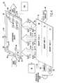
- These advanced FPGAssupport dynamic configuration and time multiplexing by employing memory slices, as shown in FIG. 3 . Each memory slice 30 , 32 and 34 contains a complete configuration of the FPGA 10 for a specific function to be performed.
- the array of the configurable logic units in the upper layer 14may be reconfigured from one application to another in a time multiplexing fashion.
- the “logic unit configuration” portion 38 , “VIA configuration” portion 40 and “user flip-flops, latching and memory” portion 42carry data in several channels, each corresponding to an active memory slice 30 , 32 or 34 .
- FPGAshave found their use in aerospace applications where they are subject to radiation and cosmic particles. All semiconductor chips, including FPGAs, aboard a craft are vulnerable since the adverse space environment potentially causes intermittent faults, a.k.a. “Single Event Upset”, and permanent faults. Radiation and cosmic particles from space tend to inject electronic charge into the FPGA circuitry which may change the state of bistable elements or may cause an unwanted impulse on a gate. These faults are considered Single Event Upsets and represent the majority of radiation faults. These faults may upset the circuitry but may not permanently damage hardware. On occasion, the charge is large enough to cause microheating. In this case, a permanent short or open circuit may occur.
- Fault free performance of programmable logic devicesis of essence not only in aero-space, but also in terrestrial applications.
- faults common to commercial FPGAswhich include metal migration faults, manufacturing faults, and faults from electrical static discharge.
- Metal migrationtends to cause short circuits and sometimes open circuits. It is a function of the temperature and the type of metals used in a chip, and may occur as the result of the chip exposition to excessive temperature over an extended period of time. Migration also occurs as the chip ages.
- Manufacturing faultsare caused by a variety of reasons, including poor grade of materials, contamination from dust particles and poor handling, etc. Although, for the most part, these faults are detected at a manufacturing facility, some of them escape screening tests.
- a primary, and at least one duplicate copyis needed for fault detection. Disagreement found in performance of the primary and duplicate circuits may manifest the presence of a fault in one of the circuits. However, it is generally impossible to judge which one of the circuits has faulted. For fault diagnosis and fault isolation, therefore, the primary and at least two duplicate circuits are needed. In this scenario, the performance of all three circuits are compared and if one of them differs it is rejected as the faulted circuit. Similarly, the primary and at least two duplicate circuits are needed for redundancy. Voting circuits interrogate all redundant circuits and the one showing a different performance is removed from operation according to a “majority principle” known to those skilled in the art.
- a single large capacity FPGA chipis often utilized.
- Such a mega FPGA chipincludes the Xilinx Virtex series and the Altera Apex series, which are being used for system chip design. Disadvantageously it is often not possible or extremely difficult to fit complete circuit duplicates within a single mega FPGA since even the mega FPGAs do not have sufficient resources to support complete multiple duplicates. Further, in practical design, the resources of the FPGA often fall short by a small percentage in meeting duplicate area requirements. For example, for triple redundancy, where 200% overhead is needed, the overhead may be 180% or 190%. It is clear therefore that redundancy in FPGAs created by separate FPGA chips or on one mega FPGA chip has extreme drawbacks.
- NASAis developing FPGA applications for space.
- the configuration of the FPGAis constantly read back as the FPGA is being used. This reading does not interfere with normal operation of the FPGA and will detect problems in the SRAM portion 12 of the FPGA which is generally the most sensitive area.
- the methoddoes not, however, cover “faults” in the circuit section 14 of the FPGA. Additionally, this method is strictly a fault detection scheme and not a fault redundancy technique.
- An additional object of the present inventionto provide a method for creating virtual circuit redundancy in FPGAs by (a) configuring, at a first time slice, a first portion of the structural elements of the FPGA into a primary circuit for a predetermined application, (b) identifying a second portion of the structural elements having the least overlap (preferably close to zero overlap) with the structural elements of the first portion, (c) configuring, at a second time slice, these zero overlap structural element of the second portion into a first duplicate circuit functionally identical to the primary circuit, (d) identifying a third portion of the plurality of structural elements having the least overlap with the structural elements involved into the primary circuit and into the first duplicate circuit, (e) configuring the third portion of the structural element into a second duplicate circuit in a third time slice, (f) repeating the steps (b)-(e) until a required number of duplicate circuits has been created in time multiplexing fashion, and (g) comparing performance of the primary circuit and all created duplicate circuits to judge which of those circuits is fault containing in order
- Another object of the present inventionis to provide a fault tolerance technique for existing dynamically reconfigurable FPGAs by creating duplicate circuits from the elements of the FPGAs unoccupied by any other primary or duplicate circuit for further interrogation thereof by a voting circuitry and by providing in these FPGAs means for identifying, at each time slice, the unused FPGA resources.
- the present inventionmay find its utility in numerous fields of application where fault tolerance is required, and particularly, in aerospace applications where semiconductor FPGAs are subject to radiation and cosmic particles, as well as in commercial applications where semiconductor FPGAs may suffer from metal migration, manufacturing shortcomings, and from poor handling.
- the present inventionis also applicable to different types of FPGAs, including particularly, so-called “embedded” chips which have non-configurable “hard-core” section and dynamically reconfigurable “soft-core” section co-located on the same chip.
- a method for creating virtual redundancy in FPGAsis provided in accordance with which, at a first time slice, a primary group of a plurality of structural elements of the FPGAs are configured into a primary circuit for a predetermined application of the FPGA, with sequential time slices following the first time slice being defined.
- each duplicate group of the plurality of structural elements of the FPGAis identified which have the least spatial overlap (preferably, zero overlap) with the primary group and with any of other duplicate groups. Then, each duplicate group is configured into a duplicate circuit functionally identical to the primary circuit so that performance of the primary circuit and of the duplicate circuits may be compared in time multiplexing fashion for determining which of the circuits is faulted for further excluding the faulted circuit from the operation of the FPGA.
- the structural elements of the FPGAmay include configurable logic units, interconnections formed on the FPGA chip, structural elements within each logical unit, and I/O units of the FPGA.
- the searchis performed for (a) unoccupied configurable logic units, and further, upon exhaustion thereof, for (b) unoccupied structural elements within occupied configurable logic units.
- Duplicate circuitsmay be arranged in different mutual spatial relationship with respect to a primary circuit, and to duplicate circuits created in other time slices.
- a duplicate circuitmay be linearly displaced from other circuits created in other time slices; or the duplicate circuit can be disposed in rotational mutual disposition with regard to other circuits created in other time slices.
- a requirementis that the spatial overlap between the structural elements of redundant circuits will have the least spatial overlap, preferably zero overlap in order to eliminate possible confusion in detecting which of the circuits contains a fault.
- the spatial displacing of the duplicate circuits with respect to the primary circuitenhances the ability to detect and isolate a fault due to a fault multiplication effect associated with use of a given faulted structural element in different circuits, which are likely to generate different responses to the same given faulted structure.
- the method of the present inventionis particularly applicable to dynamically configurable FPGAs (stand-alone chips or “embedded” FPGAs) in which multiple memory slices are used, each of which includes the whole configuration of the FPGA for a certain time period.
- FPGAsstand-alone chips or “embedded” FPGAs
- memory sliceseach of which includes the whole configuration of the FPGA for a certain time period.
- the logicmoves to another memory slice to create a primary circuit for another application and for creating the associated virtual redundancy.
- a primary circuit for a specific applicationis created, then duplicate circuits for the primary circuit for the specific application are created in time multiplexing fashion.
- the voting unitinterrogates the primary circuit and duplicate circuits with the purpose of excluding a fault containing circuit from operation.
- Another aspect of the present inventionis a FPGA having:
- configurable structural elementswhich are configurable logic units, elements within configurable logic units, routing structure, and I/O units
- the FPGAfurther includes means for selecting in each of the (1+i) th time slice the i th duplicate group of the configurable structural elements having the least overlap with structural elements occupied during 1 st through i th time slices, and
- a voting circuitfor interrogating the primary circuit and the duplicate circuits in time multiplexing fashion for comparing performance thereof for further judging which circuit includes a fault or excluding the fault containing circuit from the operation of the FPGA.
- the identification of non-overlapping structural elementsis performed, preferably, off-line on a computer work station. Once suitable structural elements are found, they are applied to the FPGA.
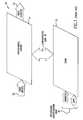
- FIG. 1is a schematic representation of a conventional FPGA
- FIG. 2is a more detailed schematic representation of a conventional FPGA
- FIG. 3is a schematic representation of a dynamically configurable FPGA of the prior art with time multiplexing feature
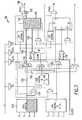
- FIG. 4is a schematic representation of the FPGA of the present invention.
- FIG. 5is a schematic representation of an FPGA showing unused resources which can be used for creation of duplicate circuits in time multiplexing fashion in accordance with the present invention
- FIGS. 6-9are electrical block diagrams of a configurable logic unit of a FPGA showing unused and hidden resources within FPGA unoccupied during forming of primary circuits for different applications;
- FIGS. 10 and 11show intersections between elements of the primary circuits of FIGS. 6-9;
- FIG. 12is a time diagram of a method of the present invention.
- FIG. 13is a schematic representation of a linearly displacement principle of the present invention.
- FIGS. 14A-14Eshow schematic representations of the rotationally displacement principle of the present invention.
- FIGS. 15-17are schematic representations of fine grained FPGAs showing creation of duplicate circuits from substantially unoccupied configurable logic units, structural elements within each configurable logic unit, and routings for achieving the virtual redundancy technique of the present invention
- FIG. 18is a flow chart diagram of an algorithm for finding orthogonal equivalents in accordance with the present invention.
- FIG. 19shows a matrix used for exhaustive search for orthogonal equivalents in accordance with the present invention.
- FIG. 20is a reduced matrix for exhaustive search for orthogonal equivalents in accordance with the method of the present invention.
- FIG. 21shows the principles of exhaustive search for orthogonal equivalents from FIG. 20 using the max-min principle.
- an FPGA 50 of the present inventionincludes a memory layer 52 , and a configurable circuit layer 54 .
- An off-line computer development workstation 56is operatively coupled to the configurable circuit layer 54 for identifying unused resources on the configurable circuit layer 54 , in order that the unused resources on the configurable circuit layer 54 may be arranged into a duplicate circuit, as will be described in detail in following paragraphs.
- the memory layer 52includes a plurality of memory slices, which in this example provides memory slice 68 , memory slice 70 , and memory slice 72 . It should be understood, however, that any number of memory slices may be contained in the memory layer 52 .
- the memory layer 52includes a plurality of memory cells each of which is accessible by data 62 supplied to a memory cell directed by the address data 64 . A particular memory slice is selected in accordance with “Select Slice” Control 66 supplied to the memory layer 52 in accordance with a required function to be performed by the FPGA 50 .
- Each memory slice 68 , 70 , and 72is coupled to the configurable circuit layer 54 through the “logic unit configuration” channel 74 , VIA configuration channel 76 and “user flip-flops, latches, and memory” channel 78 for dynamic reconfiguration of the configurable circuit 54 in accordance with a required function to be performed by the FPGA 50 .
- the circuit layer 54carries a plurality of configurable logic units 80 each of which includes elements 82 therewithin, routing structure (or interconnections) 84 , and I/O units 86 .
- the configurable circuit layer 54particularly the logic units 80 , structural elements 82 within each logic unit 80 , interconnections 84 and I/O units 86 are configured through the channels 74 , 76 and 78 to create a specific primary circuit.
- the FPGA 50utilizes resources positioned in area 100 .
- the areas 102 and 104contain resources unoccupied by the resources 100 .
- the resources 102are hidden in fragmented areas which are scattered throughout the configuration.
- the area 104represents unfragmented area resulting from a mismatch existing between the FPGA fixed chip size and the actual needed size for a specific application (which may vary from application to application).
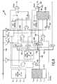
- the configurable logic unit 80includes logic function generators 110 , 112 , and 114 , and a plurality of multiplexers 116 - 124 and 139 .
- the configurable logic unit 80further includes flip-flops 125 and 126 and S/R control units 127 and 128 .
- the data contained, for example, in memory slice Aare read out to update the configuration logic unit 80 and the routing structure 84 on the chip, thereby causing the configurable logic units to perform a specific logic function. For example, as shown in FIG.
- the configurable logic unit 80is configured as an unlatched two input exclusive OR gate, which is representative of a structure corresponding to the memory slice A. It is clearly seen that only a portion of the resources of the configurable logic 80 are used, such as a portion of the logic function generator 110 , portion of multiplexers 116 and 118 , the flip-flop 125 and portion of the multiplexer 122 , as well as connections 130 - 138 . Generally, less than 50% of the configurable logic unit 80 parts are really used. Referring now to FIG.
- the configurable logic unit 80is reconfigured to perform as a non-latched 3-input AND gate wherein only the portion of the logic function generator 112 , portions of the multiplexers 139 , 121 , and 123 , and the flip-flop 126 are occupied as well as interconnections 140 - 148 . From this it is seen that only a small portion of the configurable logic unit's parts are occupied for performing the function specified in the memory slice B.
- a non-latched 3-bit parity gateis implemented in the logic unit 80 .
- the reconfigurationis carried out by invoking a portion of logic function generators 110 , 112 , and 114 , a portion of multiplexers 149 , 150 , and 117 , as well as connections 130 , 131 , and 135 common with the circuit of FIG. 7, interconnections 140 , 141 , 142 , 143 , and 153 , common with the circuit of FIG. 8, and interconnections 151 and 152 .
- FIG. 10shows elements common for memory slice A and memory slice C which include interconnections 131 , 130 and 135 .
- FIG. 11shows elements common for memory slices B and C, which include interconnections 140 , 141 , 142 , 143 , and 153 . Only a portion of core elements of the configurable logic unit 80 is used in each specific application, and a small portion of the structural elements of the configurable logic unit 80 are common to all of the circuits shown in FIGS. 7-9. Unfortunately, the configurable logic unit design in this example does not allow for completely independent circuit, as shown in FIGS. 10 and 11 where memory slices B and C, as well as memory slices A and C, have common sections.
- the basic principle of the present inventionis to employ the unoccupied resources of the FPGA for creating therefrom, in time-multiplexing fashion, duplicate circuits, so that a voting unit 160 , best shown in FIGS. 4 and 13, may compare performance of the redundant circuits for detecting the presence of a fault and for determining which circuit contains the fault in order to exclude the faulted circuit from operation of the FPGA 50 .
- a primary circuitis created at a first time slice, from the structural elements of the configurable circuit layer 54 of FIG. 4 . This may include arranging configurable logic units 80 in certain order, configuring elements 82 within logic units 80 , configuring I/O units 86 , and/or configuring interconnections 84 in a predetermined order into the primary circuit, as is shown for example in FIG. 7 .
- output datais read by the voting circuit 160 for further use in a majority voting step.
- the unit 56 of FIG. 4accomplishes the off-line search for unused resources of the configurable circuit layer 54 as will be described in detail further herein, and identifies the unused resources.
- the memory slice Aconfigures the unoccupied resources of the configurable circuit layer 54 identified during the off-line search into a first duplicate circuit functionally identical to the primary circuit, however based on structural elements having the least, preferably zero, overlap with the structural elements of the primary circuit.
- the voting circuit 160reads the output data of the first duplicate circuit for further majority voting.
- the “Select Slice” Control 66switches from the memory slice A to the memory slice B to specify function B of the FPGA 50 .
- the structural elements of the configurable circuit layer 54 of FIG. 4are rearranged into configuration corresponding to the function B, as for instance, shown in FIG. 8 .
- the sequence of operations associated with the memory slice Ais repeated with the only difference that the primary circuit and all duplicate circuits configured within the memory slice B differ from the primary circuit and all duplicate circuits configured within the memory slice A, due to the difference of the functions B and A.
- the FPGAmay be switched to the memory slice C or any other memory slice identified in the memory layer 52 and the process is repeated.
- an FPGA application 170shown in FIG. 13, includes an 8-bit register 172 connected to an AND gate 174 , which forms a primary circuit 176 of the FPGA application 170 during a first time slice.
- the FPGA 170is dynamically reconfigured to an 8-bit register 178 and an AND gate 180 for forming a first duplicate circuit 182 .
- the second configurationi.e., the first duplicate circuit 182 , purposely employs different FPGA resources, which are linearly displaced from the primary circuit 176 , i.e., displaced laterally and vertically within the configuration circuit layer of the FPGA.
- time slice 1is independent of the configuration of time slice 2 . Additionally, the spatial overlap between the resources used in the circuit 176 and the circuit 182 is substantially zero.
- a second duplicate circuit(not shown) can be configured in order to obtain triple redundancy. The third configuration (the second duplicate circuit) would also be displaced linearly from the first and second configurations 176 and 128 for attaining spatial independence therewith.
- the external voting circuit 160is coupled to the output of the AND gates 174 and 180 of the primary circuit 176 and the virtual copy 182 thereof to obtain a majority vote.
- FIGS. 14A-14EAnother way to obtain redundant equivalent circuits during off-line development is shown in FIGS. 14A-14E, where the equivalent circuits are obtained by rotating the primary application circuit geometrically.
- a primary circuit 184is formed, as shown in FIG. 14 A.
- a first duplicate circuit 186is obtained by 90°-clockwise rotation of the primary circuit 184 .
- a second duplicate circuit 188is obtained by rotating the primary circuit 184 , 180° clockwise, as shown in FIG. 14 C.
- a next duplicate copy 190is obtained by a 270° clockwise rotation of the primary circuit 184 , as shown in FIG. 14 D.
- quadruple redundancyshown in FIGS.
- the external voting circuit 160(shown in FIG. 4) is employed to obtain a majority vote of the outputs from the circuits 184 - 190 .
- the central regions of the circuits 184 , 186 , 188 and 190have overlapping resources between time slices. This means that in this particular example, the time slices are not totally independent each of the other, and therefore, a more sophisticated search for unoccupied resources is needed for rotational techniques.
- FIGS. 15-17A fine grained FPGA 194 with 25 configurable logic units 80 and via paths (routing structure) 84 is shown in FIGS. 15-17.
- Each of the configurable logic units 80includes elements 82 therewithin.
- a primary circuit 196is created in 1 st time slice, consisting of the configurable logic units a-n, in each of which only a portion of elements 82 are occupied. For example, in the logic unit a, the elements a 1 and a 4 are occupied; in unit b, the element b 3 is occupied; in the unit c, the element c 4 is occupied; in the unit d, the elements d 3 and d 4 are occupied; etc.
- a primary circuit and two duplicate copies multiplexed in three time slicesare formed. Each time slice will have a functionally equivalent circuit redundant to other equivalents.
- a computer programis used to search for suitable equivalents off-line, which may constitute a guided search, exhaustive search, or random search, as described further herein.
- FIG. 16shows a first duplicate circuit 198 created in the 2 nd nd time slice.
- this first duplicate circuit 198 created on the fine grained FPGA 194the structural elements of the FPGA are dynamically reconfigured so that to form a circuit functionally identical to the primary circuit 196 shown in FIG. 15, however containing the structural elements unoccupied by the primary circuit 196 .
- configurable logic units o through ywhich are unoccupied by the primary circuit 196 are used.
- these 11 configurable logic unitsare not a sufficient basis for functional identification to the primary circuit 196 . Therefore, configurable logic units h, l, and j of the primary circuit 196 have been identified for the duplicate circuit 198 .
- structural elements 82 used for the duplicate circuit 198are spatially independent from structural elements 82 of the primary circuit 196 , particularly, h 1 , h 2 , l 1 , j 2 , and j 3 .
- structural elements 82 used for the duplicate circuit 198are spatially independent from structural elements 82 of the primary circuit 196 , particularly, h 1 , h 2 , l 1 , j 2 , and j 3 .
- a second duplicate circuit 200is configured in the fine grained FPGA 194 , which is functionally identical to the primary circuit 196 (shown in FIG. 15) and to the duplicate circuit 198 (shown in FIG. 16 ).
- This duplicate circuit 200includes configurable logic units b, c, d, e, h, j, l, m (common with the circuit 196 ) and o, p, q, r, s, and x (common with the circuit 198 ).
- the structural elements 82 employed for the primary circuit 196 , first duplicate circuit 198 , and the second duplicate circuit 200are completely independent.
- the primary circuit 196uses the element b 3
- the second duplicate copy 200uses elements b 1 and b 4
- the element c 4is used for the primary circuit 196
- the element c 3for the duplicate copy 200
- the elements d 3 and d 4are used for the primary circuit 196 while for the second duplicate copy 200 , the element d 1 is used.
- the primary circuit 196 , first duplicate circuit 198 , and second duplicate circuit 200are completely independent in terms of used resources of the FPGA 194 .
- the primary circuit and the duplicate circuits being independentare called orthogonal equivalents. There are several algorithms developed for finding orthogonal equivalents.
- off-line development unit 56(shown in FIG. 4 ), which consists of an off-line computer workstation and development software tools for identifying the primary and duplicate configurations used by the FPGA target 50 .
- the unit 56needs to be run once for the identification process. For this reason unit 56 is operated off-line and does not need to operate in a “real-time” fashion, while the FPGA 50 is required to support real-time processing.
- the workstation (unit) 56positioned on the ground for being operatively coupled to FPGAs 50 aboard the spacecraft.
- Unit 56is a commercial off-the-shelf FPGA design software product from such companies as Mentor Graphics of Wilsonville, Oreg., or Synopsis of Mountain View, Calif. These commercial design products may be employed directly with no modification for the design virtual redundancy of the present invention; or it is possible to adapt these commercial products to yield a fully automatic design system for “virtual redundancy” of the present invention. For a large FPGA application, the design development of “virtual redundancy” may require hours of off-line computing. Once optimum configurations have been found for the primary circuit and duplicates, they are uploaded into the appropriate memory slices of the FPGA target through the channel 60 (shown in FIG. 4 ), and then multiplexed for the life cycle of the application defined in the respective memory slice 68 , 70 , or 72 .
- Constraint Inputswhich permit the user to specify critical timing constraints, physical partitions for valid FPGA areas to use, I/O pin assignments, and specific circuit locations for certain critical sections of the design,
- Placement, Routing, and FittingThis sub-system of modern development systems automatically places components within the FPGA defined positions and automatically interconnect the components using the router. More advanced development systems automatically check timing and, if necessary, make adjustments to the placing and routing procedure;
- Verification softwarewhich allows to automatically validate timing performance during the placing and routing procedure.
- the first oneutilizes commercial off-the-shelf FPGA software and significant manual effort.
- the second oneutilizes custom FPGA software and is largely automatic thus requiring no manual effort.
- the first algorithmstarts by checking if the intended application is suitable for the given FPGA. It is important that the “virtual redundancy” is applied to FPGAs having the appropriate range of unused resources. This range is constrained by upper and lower bounds. At the upper bound, when unused resources are substantially large, full parallel redundancy may be feasible thereby invalidating the need for time multiplexing the FPGA. At the lower bound, an FPGA may have very limited resources such that the virtual equivalents contain large unwanted overlap. “Virtual redundancy” is appropriate in the middle range. Thus, in the first step, the algorithm is to check that FPGA resources are a correct match for the “virtual redundancy” implementation.
- the next stepis to estimate how much overlap will occur in the virtual equivalents. Based on the estimate, the software in the unit 56 must decide which section of the circuits (primary and duplicates) will be overlapped.
- the third stepis to generate HDL (hardware description language) for the non-overlap portion of the circuit.
- HDLhardware description language
- This HDLis then copied for each of the required duplicates.
- the HDL copiesare finally given unique label names so they are not mistook with the primary HDL.
- the fourth stepis to submit all of the above HDL to the compiler (HDL for non-overlap primary, HDL for non-overlap of first duplicate, HDL for non-overlap of second duplicate, etc.).
- the compilertreats the combined HDL as one complete parallel circuit and outputs the place and routing for the composite circuit.
- the fifth stepis to separate the place and route output from the fourth step for the primary, 1st duplicate, and 2nd duplicate, etc. (this is largely a manual task).
- the sixth stepis to define the HDL for the overlap region of the circuit.
- the compileris operated in incremental mode. First, the place and route for the primary non-overlapped circuit is submitted. Then the compiler is requested to add the HDL for primary overlap circuitry. The compiler then outputs the place and route for the entire primary circuit (non-overlap and overlap regions). The resulting place and route forms the final configuration file for the first virtual equivalent.
- the eighth stepis to repeat step 7 for the first duplicate.
- the ninth stepis to repeat step 7 for the second duplicate.
- the flow chartproceeds to the logic block 220 “Input Number Copies”, where an operator inputs a desired number of redundant copies.
- the flow chartpasses to the block 230 “Input Tiring Requirement”, where the software running in the unit 56 requests timing requirements affordable for a particular application.
- the softwareverifies in the block 240 if the desired number of copies is feasible for the given timing requirements. If the requirements are in disagreement, the program reports problems in the block 250 and returns to the block 220 , where the operator inputs a different number of copies, more appropriate for the timing requirement.
- the logicflows to the block 260 “Use FPGA Compiler to Establish Primary Configuration”, where the program involves an FPGA compiler and obtains a configuration for the primary circuit copy. It is possible to use standard compiler options in the technique of the present invention.
- the softwareUpon configuring the primary circuit, the software flows to logic block 270 “Identify Unused Logic Units” in which the software running in the unit 56 searches for all unused resources, i.e., the unused configurable logic units 80 . Upon identifying all unused resources, the logic passes to the logic block 280 “Identify Complementary Logic Unit Groups with Non-Overlapping Resources” where the software identifies hidden resources, i.e., configurable logic units 80 common with the other redundant copies, however, in which non-occupied structural elements 82 are available as described with regard to FIGS. 15-17.
- a full set of configurable logic units usable for generation of the duplicate copiesare selected.
- the logicflows to the block 290 “Select Logic Units for Next Copy. First Use A New Logic Unit. Then Use Logic Units Complements”, where, based on unused logic units and complementary logic units, a full set of logic units are selected.
- the softwareflows to the block 300 “Interconnect Selected Logic Units with Unused Vias”, where the software involves a router for interconnecting the logic units in a specific order. The router is programmed to select unused vias (interconnections) 84 .
- the process of selecting unused and hidden resources and interconnecting the selected resources with unused interconnectionsis reiterated for all needed virtual copies, the number of which was entered into the software in the logic block 220 .
- the softwarepasses to the logic block 310 “Last Copy” to determine whether more copies are to be configured. If more copies are to be formed, i.e., the answer is “No”, the logic flows to the block 320 “Start Next Copy” and returns to the block 290 for selecting another group of unused and hidden resources. If, however, the last copy was generated in block 310 , the software passes to the “Stop” block 330 , where the process of generating a virtual redundancy is completed.
- the virtual redundancy techniqueis advantageous due to the high speed of reconfiguration which is in the range of microseconds, allowed by memory slicing of the FPGA capable of time multiplexing reconfigurations of logic units.
- multiplexing in FPGArequires time.
- double redundancyfor example, the overall time needed for circuit evaluation is at least doubled in comparison with situations when double redundancy is not performed.
- triple redundancythe overall time will be at least tripled. Therefore, a virtual redundancy technique is best suited for applications having generous timing margins. In addition to added time for each multiplex copy, there is additional delay resulting from the longer via paths.
- timing marginpermits other configurations to be used in the FPGA. It is clear that the larger the timing margin, the greater the number of circuit variations possible. Such timing margins depend on the application. For example, a high speed DSP (digital signal processing) application supporting fiber optic communication may have limited timing margins, whereas, an expert rule processing system may have large timing margins. Finally, as the speed of FPGAs improve, the timing margins will correspondingly increase. To summarize, application timing margin specifications limit the number of circuit equivalents. Therefore, as the timing margins increase, virtual redundancy techniques will become more practical to implement.
- the unused and hidden resourcesmay be estimated.
- FPGA design coresare available for various RISC (reduced instruction set computer), various DSP (digital signal processing) filters, and various peripheral interfaces.
- RISCreduced instruction set computer
- DSPdigital signal processing
- peripheral interfacesBy comparing the number of structural elements for example transistors, needed for a particular FPGA design core, to the equivalent ASIC design, an estimate of unused hidden resources may be established. Disadvantageously, these resources are scattered throughout the FPGA in a fragmented fashion.
- the virtual redundancy techniqueis able to exploit fractional residual space left in the FPGA at the completion of a design and also the hidden fragmented hidden space in the FPGA.
- the voting circuit 160thus is a critical element of the fault tolerance technique in any system. It is impossible to provide a completely redundant voting circuit directly on the FPGA chip since due to the fact that all output lines from primary and duplicate circuits must come to a single decision point, they all will intersect which is impermissible for all redundancy techniques. Therefore, the best strategy for fault tolerance, is to implement the voting circuit off the FPGA chip, and to make the voting circuit robust in terms of its implementation, i.e., use hard-radiation semiconductor materials with shielding.
- each duplicate copyshould provide summary data rather than exhaustive data.
- key CPU registerssuch as the memory address registers may be used.
- lock step arrangementis employed. That is, for each step and process, the summary registers are compared by the voting circuit. If they agree, the next step is initiated, in which again, the summary registers are checked. Therefore, each process step is checked and in this way, faults may be detected as early as possible.
- the virtual redundancy technique of the present inventionmay include FPGA applications in which substantially 100% of FPGA is time-multiplexed; also, in some FPGA applications only a section of the FPGA may be time-multiplexed. For example, 70% of an FPGA configuration can be static and only 30% can be time multiplexed for the purpose of virtual redundancy.
Landscapes
- Engineering & Computer Science (AREA)
- Physics & Mathematics (AREA)
- Mathematical Physics (AREA)
- General Engineering & Computer Science (AREA)
- Theoretical Computer Science (AREA)
- Computer Hardware Design (AREA)
- Computing Systems (AREA)
- Quality & Reliability (AREA)
- General Physics & Mathematics (AREA)
- Logic Circuits (AREA)
Abstract
Description
Claims (47)
Priority Applications (1)
| Application Number | Priority Date | Filing Date | Title |
|---|---|---|---|
| US09/833,712US6526559B2 (en) | 2001-04-13 | 2001-04-13 | Method for creating circuit redundancy in programmable logic devices |
Applications Claiming Priority (1)
| Application Number | Priority Date | Filing Date | Title |
|---|---|---|---|
| US09/833,712US6526559B2 (en) | 2001-04-13 | 2001-04-13 | Method for creating circuit redundancy in programmable logic devices |
Publications (2)
| Publication Number | Publication Date |
|---|---|
| US20020157071A1 US20020157071A1 (en) | 2002-10-24 |
| US6526559B2true US6526559B2 (en) | 2003-02-25 |
Family
ID=25265083
Family Applications (1)
| Application Number | Title | Priority Date | Filing Date |
|---|---|---|---|
| US09/833,712Expired - Fee RelatedUS6526559B2 (en) | 2001-04-13 | 2001-04-13 | Method for creating circuit redundancy in programmable logic devices |
Country Status (1)
| Country | Link |
|---|---|
| US (1) | US6526559B2 (en) |
Cited By (338)
| Publication number | Priority date | Publication date | Assignee | Title |
|---|---|---|---|---|
| US20030088844A1 (en)* | 2001-01-19 | 2003-05-08 | Steven Teig | Method and apparatus for pre-computing routes |
| US6624654B1 (en)* | 2002-05-16 | 2003-09-23 | Xilinx, Inc. | Methods for implementing circuits in programmable logic devices to minimize the effects of single event upsets |
| US20030223295A1 (en)* | 2002-01-17 | 2003-12-04 | Ozguz Volkan H. | Field programmable gate array with a variably wide word width memory |
| US6687884B1 (en) | 2002-05-16 | 2004-02-03 | Xilinx, Inc. | Testing for shorts between interconnect lines in a partially defective programmable logic device |
| US20040034761A1 (en)* | 2002-08-16 | 2004-02-19 | Herman Schmit | Programmable pipeline fabric utilizing partially global configuration buses |
| US20040093395A1 (en)* | 2002-03-12 | 2004-05-13 | Hitachi, Ltd. | Information system and data access method |
| US20040178819A1 (en)* | 2003-03-12 | 2004-09-16 | Xilinx, Inc. | Multi-chip programmable logic device having configurable logic circuitry and configuration data storage on different dice |
| US20040212395A1 (en)* | 2002-07-08 | 2004-10-28 | Madurawe Raminda Udaya | Three dimensional integrated circuits |
| US20040225936A1 (en)* | 2003-05-08 | 2004-11-11 | Johnson Tyler James | Voting circuit |
| US6861865B1 (en)* | 2003-03-11 | 2005-03-01 | Cavium Networks | Apparatus and method for repairing logic blocks |
| US20050125749A1 (en)* | 2003-12-05 | 2005-06-09 | International Businesss Machines Corporation | Method of selectively building redundant logic structures to improve fault tolerance |
| US20060036909A1 (en)* | 2004-08-13 | 2006-02-16 | Seakr Engineering, Incorporated | Soft error detection and recovery |
| US7036059B1 (en)* | 2001-02-14 | 2006-04-25 | Xilinx, Inc. | Techniques for mitigating, detecting and correcting single event upset effects in systems using SRAM-based field programmable gate arrays |
| US7126381B1 (en) | 2004-02-14 | 2006-10-24 | Herman Schmit | VPA interconnect circuit |
| US7126373B1 (en) | 2004-02-14 | 2006-10-24 | Herman Schmit | Configurable logic circuits with commutative properties |
| US7138827B1 (en)* | 2002-09-23 | 2006-11-21 | Xilinx, Inc. | Programmable logic device with time-multiplexed interconnect |
| US7145361B1 (en) | 2004-06-30 | 2006-12-05 | Andre Rohe | Configurable integrated circuit with different connection schemes |
| US7157933B1 (en) | 2004-02-14 | 2007-01-02 | Herman Schmit | Configurable circuits, IC's, and systems |
| US7167025B1 (en) | 2004-02-14 | 2007-01-23 | Herman Schmit | Non-sequentially configurable IC |
| US7181717B1 (en)* | 2002-05-31 | 2007-02-20 | Altera Corporation | Method and apparatus for placement of components onto programmable logic devices |
| US7193438B1 (en) | 2004-06-30 | 2007-03-20 | Andre Rohe | Configurable integrated circuit with offset connection |
| US7193440B1 (en) | 2004-02-14 | 2007-03-20 | Herman Schmit | Configurable circuits, IC's, and systems |
| US7193432B1 (en)* | 2004-02-14 | 2007-03-20 | Herman Schmit | VPA logic circuits |
| US20070075737A1 (en)* | 2004-02-14 | 2007-04-05 | Herman Schmit | Configurable Circuits, IC's, and Systems |
| US7219314B1 (en)* | 2001-08-07 | 2007-05-15 | Xilinx, Inc. | Application-specific methods for testing molectronic or nanoscale devices |
| US7224182B1 (en) | 2005-03-15 | 2007-05-29 | Brad Hutchings | Hybrid configurable circuit for a configurable IC |
| US7224181B1 (en) | 2004-11-08 | 2007-05-29 | Herman Schmit | Clock distribution in a configurable IC |
| US7242216B1 (en) | 2004-11-08 | 2007-07-10 | Herman Schmit | Embedding memory between tile arrangement of a configurable IC |
| US7254801B1 (en)* | 2005-01-20 | 2007-08-07 | Altera Corporation | Synthesis aware placement: a novel approach that combines knowledge of possible resynthesis |
| US7259587B1 (en) | 2004-11-08 | 2007-08-21 | Tabula, Inc. | Configurable IC's with configurable logic resources that have asymetric inputs and/or outputs |
| US7268586B1 (en) | 2004-11-08 | 2007-09-11 | Tabula, Inc. | Method and apparatus for accessing stored data in a reconfigurable IC |
| US7276933B1 (en) | 2004-11-08 | 2007-10-02 | Tabula, Inc. | Reconfigurable IC that has sections running at different looperness |
| US7282950B1 (en) | 2004-11-08 | 2007-10-16 | Tabula, Inc. | Configurable IC's with logic resources with offset connections |
| US7284222B1 (en) | 2004-06-30 | 2007-10-16 | Tabula, Inc. | Method and apparatus for identifying connections between configurable nodes in a configurable integrated circuit |
| US20070244959A1 (en)* | 2005-03-15 | 2007-10-18 | Steven Teig | Configurable IC's with dual carry chains |
| US20070241776A1 (en)* | 2004-06-30 | 2007-10-18 | Herman Schmit | Configurable Logic Circuits with Commutative Properties |
| US20070241788A1 (en)* | 2004-06-30 | 2007-10-18 | Herman Schmit | VPA Logic Circuits |
| US20070241773A1 (en)* | 2005-03-15 | 2007-10-18 | Brad Hutchings | Hybrid logic/interconnect circuit in a configurable ic |
| US20070241781A1 (en)* | 2005-03-15 | 2007-10-18 | Brad Hutchings | Variable width management for a memory of a configurable IC |
| US20070241787A1 (en)* | 2004-06-30 | 2007-10-18 | Herman Schmit | Configurable Circuits, IC's, and Systems |
| US20070241784A1 (en)* | 2005-03-15 | 2007-10-18 | Brad Hutchings | Configurable ic with interconnect circuits that have select lines driven by user signals |
| US20070257700A1 (en)* | 2005-03-15 | 2007-11-08 | Andrew Caldwell | Method and apparatus for decomposing functions in a configurable IC |
| US7295037B2 (en) | 2004-11-08 | 2007-11-13 | Tabula, Inc. | Configurable IC with routing circuits with offset connections |
| US7301368B2 (en) | 2005-03-15 | 2007-11-27 | Tabula, Inc. | Embedding memory within tile arrangement of a configurable IC |
| US7312630B2 (en) | 2004-06-30 | 2007-12-25 | Tabula, Inc. | Configurable integrated circuit with built-in turns |
| US7317331B2 (en) | 2004-11-08 | 2008-01-08 | Tabula, Inc. | Reconfigurable IC that has sections running at different reconfiguration rates |
| US7327159B1 (en)* | 2005-11-28 | 2008-02-05 | Lattice Semiconductor Corporation | Interface block architectures |
| US7330050B2 (en) | 2004-11-08 | 2008-02-12 | Tabula, Inc. | Storage elements for a configurable IC and method and apparatus for accessing data stored in the storage elements |
| US7342415B2 (en) | 2004-11-08 | 2008-03-11 | Tabula, Inc. | Configurable IC with interconnect circuits that also perform storage operations |
| US20080074144A1 (en)* | 2002-01-17 | 2008-03-27 | Volkan Ozguz | Field programmable gate array utilizing dedicated memory stacks in a vertical layer format |
| WO2008011232A3 (en)* | 2006-06-07 | 2008-05-02 | Bae Systems Information | Universal non-volatile support device for supporting reconfigurable processing systems |
| US7372297B1 (en) | 2005-11-07 | 2008-05-13 | Tabula Inc. | Hybrid interconnect/logic circuits enabling efficient replication of a function in several sub-cycles to save logic and routing resources |
| US20080129336A1 (en)* | 2004-02-14 | 2008-06-05 | Herman Schmit | Via programmable gate array with offset direct connections |
| US7394708B1 (en) | 2005-03-18 | 2008-07-01 | Xilinx, Inc. | Adjustable global tap voltage to improve memory cell yield |
| US20080184057A1 (en)* | 2007-01-31 | 2008-07-31 | Tyler Thorp | Methods and apparatus for employing redundant arrays to configure non-volatile memory |
| US20080184065A1 (en)* | 2007-01-31 | 2008-07-31 | Tyler Thorp | Methods and apparatus for employing redundant arrays to configure non-volatile memory |
| US20080189448A1 (en)* | 2007-02-07 | 2008-08-07 | Honeywell International Inc. | Method for implementing a control channel in a system of circumvention and recovery |
| US7425841B2 (en) | 2004-02-14 | 2008-09-16 | Tabula Inc. | Configurable circuits, IC's, and systems |
| US20080231318A1 (en)* | 2007-03-20 | 2008-09-25 | Herman Schmit | Configurable ic having a routing fabric with storage elements |
| US20080256375A1 (en)* | 2007-04-12 | 2008-10-16 | Honeywell International Inc. | System of integrated environmenatlly hardened architecture for space application |
| US7444565B1 (en)* | 2003-11-24 | 2008-10-28 | Itt Manufacturing Enterprises, Inc. | Re-programmable COMSEC module |
| US7461362B1 (en) | 2005-12-01 | 2008-12-02 | Tabula, Inc. | Replacing circuit design elements with their equivalents |
| US20080301345A1 (en)* | 2007-05-29 | 2008-12-04 | Blinick Stephen L | Multi-character adapter card |
| US7489162B1 (en) | 2005-12-01 | 2009-02-10 | Tabula, Inc. | Users registers in a reconfigurable IC |
| US7504858B1 (en) | 2006-03-08 | 2009-03-17 | Tabula, Inc. | Configurable integrated circuit with parallel non-neighboring offset connections |
| US7518400B1 (en) | 2006-03-08 | 2009-04-14 | Tabula, Inc. | Barrel shifter implemented on a configurable integrated circuit |
| US20090096481A1 (en)* | 2007-10-10 | 2009-04-16 | International Business Machines Corporation | Scheduler design to optimize system performance using configurable acceleration engines |
| US7529992B1 (en) | 2006-03-27 | 2009-05-05 | Tabula, Inc. | Configurable integrated circuit with error correcting circuitry |
| US7535252B1 (en) | 2007-03-22 | 2009-05-19 | Tabula, Inc. | Configurable ICs that conditionally transition through configuration data sets |
| US20090128189A1 (en)* | 2007-11-19 | 2009-05-21 | Raminda Udaya Madurawe | Three dimensional programmable devices |
| US20090134909A1 (en)* | 2003-12-04 | 2009-05-28 | Raminda Udaya Madurawe | Programmable structured arrays |
| US20090146689A1 (en)* | 2007-09-06 | 2009-06-11 | Trevis Chandler | Configuration Context Switcher with a Clocked Storage Element |
| US20090146189A1 (en)* | 2007-11-19 | 2009-06-11 | Raminda Udaya Madurawe | Pads and pin-outs in three dimensional integrated circuits |
| US7573296B2 (en) | 2004-11-08 | 2009-08-11 | Tabula Inc. | Configurable IC with configurable routing resources that have asymmetric input and/or outputs |
| US7587697B1 (en) | 2006-12-12 | 2009-09-08 | Tabula, Inc. | System and method of mapping memory blocks in a configurable integrated circuit |
| US7587698B1 (en) | 2004-12-01 | 2009-09-08 | Tabula Inc. | Operational time extension |
| US7609085B1 (en) | 2006-03-08 | 2009-10-27 | Tabula, Inc. | Configurable integrated circuit with a 4-to-1 multiplexer |
| US7626419B1 (en) | 2005-11-11 | 2009-12-01 | Tabula, Inc. | Via programmable gate array with offset bit lines |
| US20090327987A1 (en)* | 2008-06-26 | 2009-12-31 | Steven Teig | Timing operations in an IC with configurable circuits |
| US7644386B1 (en)* | 2004-05-28 | 2010-01-05 | Altera Corporation | Redundancy structures and methods in a programmable logic device |
| US7669097B1 (en) | 2006-03-27 | 2010-02-23 | Tabula, Inc. | Configurable IC with error detection and correction circuitry |
| US7679401B1 (en) | 2005-12-01 | 2010-03-16 | Tabula, Inc. | User registers implemented with routing circuits in a configurable IC |
| US7694083B1 (en) | 2006-03-08 | 2010-04-06 | Tabula, Inc. | System and method for providing a virtual memory architecture narrower and deeper than a physical memory architecture |
| US7743085B2 (en) | 2004-11-08 | 2010-06-22 | Tabula, Inc. | Configurable IC with large carry chains |
| US7757197B1 (en)* | 2003-05-29 | 2010-07-13 | Altera Corporation | Method and apparatus for utilizing constraints for the routing of a design on a programmable logic device |
| US7765249B1 (en) | 2005-11-07 | 2010-07-27 | Tabula, Inc. | Use of hybrid interconnect/logic circuits for multiplication |
| US7797497B1 (en) | 2006-03-08 | 2010-09-14 | Tabula, Inc. | System and method for providing more logical memory ports than physical memory ports |
| US7804730B2 (en) | 2005-03-15 | 2010-09-28 | Tabula, Inc. | Method and apparatus for accessing contents of memory cells |
| US7818361B1 (en) | 2005-11-07 | 2010-10-19 | Tabula, Inc. | Method and apparatus for performing two's complement multiplication |
| US7852107B1 (en)* | 2010-02-18 | 2010-12-14 | Xilinx, Inc. | Single event upset mitigation |
| US20110037497A1 (en)* | 2009-04-14 | 2011-02-17 | Or-Ment Llc | Method for Fabrication of a Semiconductor Device and Structure |
| US20110049577A1 (en)* | 2009-04-14 | 2011-03-03 | NuPGA Corporation | System comprising a semiconductor device and structure |
| US7906984B1 (en) | 2008-02-26 | 2011-03-15 | The United States Of America As Represented By The Secretary Of The Air Force | Relocatable field programmable gate array bitstreams for fault tolerance |
| US7917559B2 (en) | 2004-11-08 | 2011-03-29 | Tabula, Inc. | Configurable IC's with configurable logic circuits that perform adder and/or subtractor operations |
| US20110084314A1 (en)* | 2009-10-12 | 2011-04-14 | NuPGA Corporation | System comprising a semiconductor device and structure |
| US7930666B1 (en) | 2006-12-12 | 2011-04-19 | Tabula, Inc. | System and method of providing a memory hierarchy |
| US20110092030A1 (en)* | 2009-04-14 | 2011-04-21 | NuPGA Corporation | System comprising a semiconductor device and structure |
| US20110108888A1 (en)* | 2009-04-14 | 2011-05-12 | NuPGA Corporation | System comprising a semiconductor device and structure |
| US20110121366A1 (en)* | 2009-04-14 | 2011-05-26 | NuPGA Corporation | System comprising a semiconductor device and structure |
| US20110187409A1 (en)* | 2010-02-01 | 2011-08-04 | Renesas Electronics Corporation | Reconfigurable semiconductor integrated circuit |
| US20110221471A1 (en)* | 2008-09-17 | 2011-09-15 | Jason Redgrave | Controllable storage elements for an ic |
| US20110283250A1 (en)* | 2010-05-11 | 2011-11-17 | Altera Corporation | Method and apparatus for performing asynchronous and synchronous reset removal during synthesis |
| US8203148B2 (en) | 2010-10-11 | 2012-06-19 | Monolithic 3D Inc. | Semiconductor device and structure |
| US20120194218A1 (en)* | 2010-09-30 | 2012-08-02 | Zvi Or-Bach | 3D Semiconductor Device |
| USRE43619E1 (en)* | 2001-08-11 | 2012-08-28 | Ramsle Technology Group Gmbh, Llc | Universal computer architecture |
| US8273610B2 (en) | 2010-11-18 | 2012-09-25 | Monolithic 3D Inc. | Method of constructing a semiconductor device and structure |
| US8294159B2 (en) | 2009-10-12 | 2012-10-23 | Monolithic 3D Inc. | Method for fabrication of a semiconductor device and structure |
| US20120306535A1 (en)* | 2011-06-02 | 2012-12-06 | Arizona Board Of Regents For And On Behalf Of Arizona State University | Structures and methods for design automation of radiation hardened triple mode redundant digital circuits |
| US8358154B2 (en) | 2010-10-29 | 2013-01-22 | Honeywell International Inc. | Magnetic logic gate |
| US8358149B2 (en) | 2010-10-29 | 2013-01-22 | Honeywell International Inc. | Magnetic logic gate |
| US8362800B2 (en) | 2010-10-13 | 2013-01-29 | Monolithic 3D Inc. | 3D semiconductor device including field repairable logics |
| US8374020B2 (en) | 2010-10-29 | 2013-02-12 | Honeywell International Inc. | Reduced switching-energy magnetic elements |
| US8373230B1 (en) | 2010-10-13 | 2013-02-12 | Monolithic 3D Inc. | Method for fabrication of a semiconductor device and structure |
| US8373439B2 (en) | 2009-04-14 | 2013-02-12 | Monolithic 3D Inc. | 3D semiconductor device |
| US8379458B1 (en) | 2010-10-13 | 2013-02-19 | Monolithic 3D Inc. | Semiconductor device and structure |
| US8378494B2 (en) | 2009-04-14 | 2013-02-19 | Monolithic 3D Inc. | Method for fabrication of a semiconductor device and structure |
| US8378715B2 (en) | 2009-04-14 | 2013-02-19 | Monolithic 3D Inc. | Method to construct systems |
| US8397191B1 (en)* | 2011-11-07 | 2013-03-12 | Xilinx, Inc. | Determining failure rate from circuit design layouts |
| US8427197B2 (en) | 2011-06-15 | 2013-04-23 | Honeywell International Inc. | Configurable reference circuit for logic gates |
| US8427199B2 (en) | 2010-10-29 | 2013-04-23 | Honeywell International Inc. | Magnetic logic gate |
| US8427200B2 (en) | 2009-04-14 | 2013-04-23 | Monolithic 3D Inc. | 3D semiconductor device |
| US8440542B2 (en) | 2010-10-11 | 2013-05-14 | Monolithic 3D Inc. | Semiconductor device and structure |
| US8450804B2 (en) | 2011-03-06 | 2013-05-28 | Monolithic 3D Inc. | Semiconductor device and structure for heat removal |
| US8463836B1 (en) | 2005-11-07 | 2013-06-11 | Tabula, Inc. | Performing mathematical and logical operations in multiple sub-cycles |
| US8461035B1 (en) | 2010-09-30 | 2013-06-11 | Monolithic 3D Inc. | Method for fabrication of a semiconductor device and structure |
| US8476145B2 (en) | 2010-10-13 | 2013-07-02 | Monolithic 3D Inc. | Method of fabricating a semiconductor device and structure |
| US8492886B2 (en) | 2010-02-16 | 2013-07-23 | Monolithic 3D Inc | 3D integrated circuit with logic |
| US8522091B1 (en) | 2011-11-18 | 2013-08-27 | Xilinx, Inc. | Prioritized detection of memory corruption |
| US8536023B2 (en) | 2010-11-22 | 2013-09-17 | Monolithic 3D Inc. | Method of manufacturing a semiconductor device and structure |
| US8541819B1 (en) | 2010-12-09 | 2013-09-24 | Monolithic 3D Inc. | Semiconductor device and structure |
| US8549379B2 (en) | 2010-11-19 | 2013-10-01 | Xilinx, Inc. | Classifying a criticality of a soft error and mitigating the soft error based on the criticality |
| US8557632B1 (en) | 2012-04-09 | 2013-10-15 | Monolithic 3D Inc. | Method for fabrication of a semiconductor device and structure |
| US8574929B1 (en) | 2012-11-16 | 2013-11-05 | Monolithic 3D Inc. | Method to form a 3D semiconductor device and structure |
| US8581349B1 (en) | 2011-05-02 | 2013-11-12 | Monolithic 3D Inc. | 3D memory semiconductor device and structure |
| US8642416B2 (en) | 2010-07-30 | 2014-02-04 | Monolithic 3D Inc. | Method of forming three dimensional integrated circuit devices using layer transfer technique |
| US8669778B1 (en) | 2009-04-14 | 2014-03-11 | Monolithic 3D Inc. | Method for design and manufacturing of a 3D semiconductor device |
| US8674470B1 (en) | 2012-12-22 | 2014-03-18 | Monolithic 3D Inc. | Semiconductor device and structure |
| US8686428B1 (en) | 2012-11-16 | 2014-04-01 | Monolithic 3D Inc. | Semiconductor device and structure |
| US8687399B2 (en) | 2011-10-02 | 2014-04-01 | Monolithic 3D Inc. | Semiconductor device and structure |
| US8709880B2 (en) | 2010-07-30 | 2014-04-29 | Monolithic 3D Inc | Method for fabrication of a semiconductor device and structure |
| US8742476B1 (en) | 2012-11-27 | 2014-06-03 | Monolithic 3D Inc. | Semiconductor device and structure |
| US8753913B2 (en) | 2010-10-13 | 2014-06-17 | Monolithic 3D Inc. | Method for fabricating novel semiconductor and optoelectronic devices |
| US8803206B1 (en) | 2012-12-29 | 2014-08-12 | Monolithic 3D Inc. | 3D semiconductor device and structure |
| US8863067B1 (en) | 2008-02-06 | 2014-10-14 | Tabula, Inc. | Sequential delay analysis by placement engines |
| US8902663B1 (en) | 2013-03-11 | 2014-12-02 | Monolithic 3D Inc. | Method of maintaining a memory state |
| US8901613B2 (en) | 2011-03-06 | 2014-12-02 | Monolithic 3D Inc. | Semiconductor device and structure for heat removal |
| US8975670B2 (en) | 2011-03-06 | 2015-03-10 | Monolithic 3D Inc. | Semiconductor device and structure for heat removal |
| US8994404B1 (en) | 2013-03-12 | 2015-03-31 | Monolithic 3D Inc. | Semiconductor device and structure |
| US9000557B2 (en) | 2012-03-17 | 2015-04-07 | Zvi Or-Bach | Semiconductor device and structure |
| US9029173B2 (en) | 2011-10-18 | 2015-05-12 | Monolithic 3D Inc. | Method for fabrication of a semiconductor device and structure |
| US9041429B2 (en) | 2011-06-02 | 2015-05-26 | Arizona Board Of Regents, A Body Corporate Of The State Of Arizona, Acting For And On Behalf Of Arizona State University | Sequential state elements for triple-mode redundant state machines, related methods, and systems |
| US9054688B2 (en) | 2012-09-19 | 2015-06-09 | Arizona Board Of Regents, A Body Corporate Of The State Of Arizona, Acting For And On Behalf Of Arizona State University | Sequential state elements radiation hardened by design |
| US9087169B2 (en) | 2008-09-14 | 2015-07-21 | Raminda U. Madurawe | Automated metal pattern generation for integrated circuits |
| US9099424B1 (en) | 2012-08-10 | 2015-08-04 | Monolithic 3D Inc. | Semiconductor system, device and structure with heat removal |
| US9099526B2 (en) | 2010-02-16 | 2015-08-04 | Monolithic 3D Inc. | Integrated circuit device and structure |
| US9117749B1 (en) | 2013-03-15 | 2015-08-25 | Monolithic 3D Inc. | Semiconductor device and structure |
| US9197804B1 (en) | 2011-10-14 | 2015-11-24 | Monolithic 3D Inc. | Semiconductor and optoelectronic devices |
| US9219005B2 (en) | 2011-06-28 | 2015-12-22 | Monolithic 3D Inc. | Semiconductor system and device |
| US9362913B1 (en) | 2014-09-26 | 2016-06-07 | Altera Corporation | Circuitry for implementing multi-mode redundancy and arithmetic functions |
| US9509313B2 (en) | 2009-04-14 | 2016-11-29 | Monolithic 3D Inc. | 3D semiconductor device |
| US9547736B2 (en) | 2002-07-08 | 2017-01-17 | Callahan Cellular L.L.C. | Timing exact design conversions from FPGA to ASIC |
| US9577642B2 (en) | 2009-04-14 | 2017-02-21 | Monolithic 3D Inc. | Method to form a 3D semiconductor device |
| US9583190B2 (en) | 2011-11-11 | 2017-02-28 | Altera Corporation | Content addressable memory in integrated circuit |
| US20170074930A1 (en)* | 2015-09-15 | 2017-03-16 | Texas Instruments Incorporated | Integrated circuit chip with multiple cores |
| US9734272B2 (en) | 2014-06-13 | 2017-08-15 | Arizona Board Of Regents On Behalf Of Arizona State University | Techniques for generating physical layouts of in silico multi mode integrated circuits |
| US9871034B1 (en) | 2012-12-29 | 2018-01-16 | Monolithic 3D Inc. | Semiconductor device and structure |
| US9953925B2 (en) | 2011-06-28 | 2018-04-24 | Monolithic 3D Inc. | Semiconductor system and device |
| US10043781B2 (en) | 2009-10-12 | 2018-08-07 | Monolithic 3D Inc. | 3D semiconductor device and structure |
| US10115663B2 (en) | 2012-12-29 | 2018-10-30 | Monolithic 3D Inc. | 3D semiconductor device and structure |
| US10127344B2 (en) | 2013-04-15 | 2018-11-13 | Monolithic 3D Inc. | Automation for monolithic 3D devices |
| US10157909B2 (en) | 2009-10-12 | 2018-12-18 | Monolithic 3D Inc. | 3D semiconductor device and structure |
| US10217667B2 (en) | 2011-06-28 | 2019-02-26 | Monolithic 3D Inc. | 3D semiconductor device, fabrication method and system |
| US10224279B2 (en) | 2013-03-15 | 2019-03-05 | Monolithic 3D Inc. | Semiconductor device and structure |
| US10290682B2 (en) | 2010-10-11 | 2019-05-14 | Monolithic 3D Inc. | 3D IC semiconductor device and structure with stacked memory |
| US10297586B2 (en) | 2015-03-09 | 2019-05-21 | Monolithic 3D Inc. | Methods for processing a 3D semiconductor device |
| US10325651B2 (en) | 2013-03-11 | 2019-06-18 | Monolithic 3D Inc. | 3D semiconductor device with stacked memory |
| US10354995B2 (en) | 2009-10-12 | 2019-07-16 | Monolithic 3D Inc. | Semiconductor memory device and structure |
| US10366970B2 (en) | 2009-10-12 | 2019-07-30 | Monolithic 3D Inc. | 3D semiconductor device and structure |
| US10381328B2 (en) | 2015-04-19 | 2019-08-13 | Monolithic 3D Inc. | Semiconductor device and structure |
| US10388863B2 (en) | 2009-10-12 | 2019-08-20 | Monolithic 3D Inc. | 3D memory device and structure |
| US10388568B2 (en) | 2011-06-28 | 2019-08-20 | Monolithic 3D Inc. | 3D semiconductor device and system |
| US10418369B2 (en) | 2015-10-24 | 2019-09-17 | Monolithic 3D Inc. | Multi-level semiconductor memory device and structure |
| US10497713B2 (en) | 2010-11-18 | 2019-12-03 | Monolithic 3D Inc. | 3D semiconductor memory device and structure |
| US10515981B2 (en) | 2015-09-21 | 2019-12-24 | Monolithic 3D Inc. | Multilevel semiconductor device and structure with memory |
| US10522225B1 (en) | 2015-10-02 | 2019-12-31 | Monolithic 3D Inc. | Semiconductor device with non-volatile memory |
| US20200019477A1 (en)* | 2018-07-10 | 2020-01-16 | Qualcomm Incorporated | Diverse redundant processing modules for error detection |
| US10579536B2 (en) | 2016-08-09 | 2020-03-03 | Arizona Board Of Regents On Behalf Of Arizona State University | Multi-mode radiation hardened multi-core microprocessors |
| US10600657B2 (en) | 2012-12-29 | 2020-03-24 | Monolithic 3D Inc | 3D semiconductor device and structure |
| US10600888B2 (en) | 2012-04-09 | 2020-03-24 | Monolithic 3D Inc. | 3D semiconductor device |
| US10651054B2 (en) | 2012-12-29 | 2020-05-12 | Monolithic 3D Inc. | 3D semiconductor device and structure |
| US10679977B2 (en) | 2010-10-13 | 2020-06-09 | Monolithic 3D Inc. | 3D microdisplay device and structure |
| US10825779B2 (en) | 2015-04-19 | 2020-11-03 | Monolithic 3D Inc. | 3D semiconductor device and structure |
| US10833108B2 (en) | 2010-10-13 | 2020-11-10 | Monolithic 3D Inc. | 3D microdisplay device and structure |
| US10840239B2 (en) | 2014-08-26 | 2020-11-17 | Monolithic 3D Inc. | 3D semiconductor device and structure |
| US10847540B2 (en) | 2015-10-24 | 2020-11-24 | Monolithic 3D Inc. | 3D semiconductor memory device and structure |
| US10892169B2 (en) | 2012-12-29 | 2021-01-12 | Monolithic 3D Inc. | 3D semiconductor device and structure |
| US10892016B1 (en) | 2019-04-08 | 2021-01-12 | Monolithic 3D Inc. | 3D memory semiconductor devices and structures |
| US10896931B1 (en) | 2010-10-11 | 2021-01-19 | Monolithic 3D Inc. | 3D semiconductor device and structure |
| US10903089B1 (en) | 2012-12-29 | 2021-01-26 | Monolithic 3D Inc. | 3D semiconductor device and structure |
| US10910364B2 (en) | 2009-10-12 | 2021-02-02 | Monolitaic 3D Inc. | 3D semiconductor device |
| US10943934B2 (en) | 2010-10-13 | 2021-03-09 | Monolithic 3D Inc. | Multilevel semiconductor device and structure |
| US10978501B1 (en) | 2010-10-13 | 2021-04-13 | Monolithic 3D Inc. | Multilevel semiconductor device and structure with waveguides |
| US10998374B1 (en) | 2010-10-13 | 2021-05-04 | Monolithic 3D Inc. | Multilevel semiconductor device and structure |
| US11004719B1 (en) | 2010-11-18 | 2021-05-11 | Monolithic 3D Inc. | Methods for producing a 3D semiconductor memory device and structure |
| US11004694B1 (en) | 2012-12-29 | 2021-05-11 | Monolithic 3D Inc. | 3D semiconductor device and structure |
| US11011507B1 (en) | 2015-04-19 | 2021-05-18 | Monolithic 3D Inc. | 3D semiconductor device and structure |
| US11018133B2 (en) | 2009-10-12 | 2021-05-25 | Monolithic 3D Inc. | 3D integrated circuit |
| US11018191B1 (en) | 2010-10-11 | 2021-05-25 | Monolithic 3D Inc. | 3D semiconductor device and structure |
| US11018042B1 (en) | 2010-11-18 | 2021-05-25 | Monolithic 3D Inc. | 3D semiconductor memory device and structure |
| US11018116B2 (en) | 2012-12-22 | 2021-05-25 | Monolithic 3D Inc. | Method to form a 3D semiconductor device and structure |
| US11018156B2 (en) | 2019-04-08 | 2021-05-25 | Monolithic 3D Inc. | 3D memory semiconductor devices and structures |
| US11024673B1 (en) | 2010-10-11 | 2021-06-01 | Monolithic 3D Inc. | 3D semiconductor device and structure |
| US11031394B1 (en) | 2014-01-28 | 2021-06-08 | Monolithic 3D Inc. | 3D semiconductor device and structure |
| US11031275B2 (en) | 2010-11-18 | 2021-06-08 | Monolithic 3D Inc. | 3D semiconductor device and structure with memory |
| US11030371B2 (en) | 2013-04-15 | 2021-06-08 | Monolithic 3D Inc. | Automation for monolithic 3D devices |
| US11043523B1 (en) | 2010-10-13 | 2021-06-22 | Monolithic 3D Inc. | Multilevel semiconductor device and structure with image sensors |
| US11056468B1 (en) | 2015-04-19 | 2021-07-06 | Monolithic 3D Inc. | 3D semiconductor device and structure |
| US11063024B1 (en) | 2012-12-22 | 2021-07-13 | Monlithic 3D Inc. | Method to form a 3D semiconductor device and structure |
| US11063071B1 (en) | 2010-10-13 | 2021-07-13 | Monolithic 3D Inc. | Multilevel semiconductor device and structure with waveguides |
| US11087995B1 (en) | 2012-12-29 | 2021-08-10 | Monolithic 3D Inc. | 3D semiconductor device and structure |
| US11088130B2 (en) | 2014-01-28 | 2021-08-10 | Monolithic 3D Inc. | 3D semiconductor device and structure |
| US11088050B2 (en) | 2012-04-09 | 2021-08-10 | Monolithic 3D Inc. | 3D semiconductor device with isolation layers |
| US11094576B1 (en) | 2010-11-18 | 2021-08-17 | Monolithic 3D Inc. | Methods for producing a 3D semiconductor memory device and structure |
| US11107721B2 (en) | 2010-11-18 | 2021-08-31 | Monolithic 3D Inc. | 3D semiconductor device and structure with NAND logic |
| US11107808B1 (en) | 2014-01-28 | 2021-08-31 | Monolithic 3D Inc. | 3D semiconductor device and structure |
| US11114427B2 (en) | 2015-11-07 | 2021-09-07 | Monolithic 3D Inc. | 3D semiconductor processor and memory device and structure |
| US11114464B2 (en) | 2015-10-24 | 2021-09-07 | Monolithic 3D Inc. | 3D semiconductor device and structure |
| US11121021B2 (en) | 2010-11-18 | 2021-09-14 | Monolithic 3D Inc. | 3D semiconductor device and structure |
| US11133344B2 (en) | 2010-10-13 | 2021-09-28 | Monolithic 3D Inc. | Multilevel semiconductor device and structure with image sensors |
| US11158674B2 (en) | 2010-10-11 | 2021-10-26 | Monolithic 3D Inc. | Method to produce a 3D semiconductor device and structure |
| US11158652B1 (en) | 2019-04-08 | 2021-10-26 | Monolithic 3D Inc. | 3D memory semiconductor devices and structures |
| US11164811B2 (en) | 2012-04-09 | 2021-11-02 | Monolithic 3D Inc. | 3D semiconductor device with isolation layers and oxide-to-oxide bonding |
| US11164898B2 (en) | 2010-10-13 | 2021-11-02 | Monolithic 3D Inc. | Multilevel semiconductor device and structure |
| US11164770B1 (en) | 2010-11-18 | 2021-11-02 | Monolithic 3D Inc. | Method for producing a 3D semiconductor memory device and structure |
| US11163112B2 (en) | 2010-10-13 | 2021-11-02 | Monolithic 3D Inc. | Multilevel semiconductor device and structure with electromagnetic modulators |
| US11177140B2 (en) | 2012-12-29 | 2021-11-16 | Monolithic 3D Inc. | 3D semiconductor device and structure |
| US11211279B2 (en) | 2010-11-18 | 2021-12-28 | Monolithic 3D Inc. | Method for processing a 3D integrated circuit and structure |
| US11217565B2 (en) | 2012-12-22 | 2022-01-04 | Monolithic 3D Inc. | Method to form a 3D semiconductor device and structure |
| US11227897B2 (en) | 2010-10-11 | 2022-01-18 | Monolithic 3D Inc. | Method for producing a 3D semiconductor memory device and structure |
| US11251149B2 (en) | 2016-10-10 | 2022-02-15 | Monolithic 3D Inc. | 3D memory device and structure |
| US11257867B1 (en) | 2010-10-11 | 2022-02-22 | Monolithic 3D Inc. | 3D semiconductor device and structure with oxide bonds |
| US11270055B1 (en) | 2013-04-15 | 2022-03-08 | Monolithic 3D Inc. | Automation for monolithic 3D devices |
| US11296106B2 (en) | 2019-04-08 | 2022-04-05 | Monolithic 3D Inc. | 3D memory semiconductor devices and structures |
| US11296115B1 (en) | 2015-10-24 | 2022-04-05 | Monolithic 3D Inc. | 3D semiconductor device and structure |
| US11309292B2 (en) | 2012-12-22 | 2022-04-19 | Monolithic 3D Inc. | 3D semiconductor device and structure with metal layers |
| US11315980B1 (en) | 2010-10-11 | 2022-04-26 | Monolithic 3D Inc. | 3D semiconductor device and structure with transistors |
| US11327227B2 (en) | 2010-10-13 | 2022-05-10 | Monolithic 3D Inc. | Multilevel semiconductor device and structure with electromagnetic modulators |
| US11329059B1 (en) | 2016-10-10 | 2022-05-10 | Monolithic 3D Inc. | 3D memory devices and structures with thinned single crystal substrates |
| US11341309B1 (en) | 2013-04-15 | 2022-05-24 | Monolithic 3D Inc. | Automation for monolithic 3D devices |
| US11355380B2 (en) | 2010-11-18 | 2022-06-07 | Monolithic 3D Inc. | Methods for producing 3D semiconductor memory device and structure utilizing alignment marks |
| US11355381B2 (en) | 2010-11-18 | 2022-06-07 | Monolithic 3D Inc. | 3D semiconductor memory device and structure |
| US11374118B2 (en) | 2009-10-12 | 2022-06-28 | Monolithic 3D Inc. | Method to form a 3D integrated circuit |
| US11398569B2 (en) | 2013-03-12 | 2022-07-26 | Monolithic 3D Inc. | 3D semiconductor device and structure |
| US11404466B2 (en) | 2010-10-13 | 2022-08-02 | Monolithic 3D Inc. | Multilevel semiconductor device and structure with image sensors |
| US11410912B2 (en) | 2012-04-09 | 2022-08-09 | Monolithic 3D Inc. | 3D semiconductor device with vias and isolation layers |
| US11424621B2 (en) | 2020-01-28 | 2022-08-23 | Qualcomm Incorporated | Configurable redundant systems for safety critical applications |
| US11430667B2 (en) | 2012-12-29 | 2022-08-30 | Monolithic 3D Inc. | 3D semiconductor device and structure with bonding |
| US11430668B2 (en) | 2012-12-29 | 2022-08-30 | Monolithic 3D Inc. | 3D semiconductor device and structure with bonding |
| US11437368B2 (en) | 2010-10-13 | 2022-09-06 | Monolithic 3D Inc. | Multilevel semiconductor device and structure with oxide bonding |
| US11443971B2 (en) | 2010-11-18 | 2022-09-13 | Monolithic 3D Inc. | 3D semiconductor device and structure with memory |
| US11469271B2 (en) | 2010-10-11 | 2022-10-11 | Monolithic 3D Inc. | Method to produce 3D semiconductor devices and structures with memory |
| US11476181B1 (en) | 2012-04-09 | 2022-10-18 | Monolithic 3D Inc. | 3D semiconductor device and structure with metal layers |
| US11482438B2 (en) | 2010-11-18 | 2022-10-25 | Monolithic 3D Inc. | Methods for producing a 3D semiconductor memory device and structure |
| US11482440B2 (en) | 2010-12-16 | 2022-10-25 | Monolithic 3D Inc. | 3D semiconductor device and structure with a built-in test circuit for repairing faulty circuits |
| US11482439B2 (en) | 2010-11-18 | 2022-10-25 | Monolithic 3D Inc. | Methods for producing a 3D semiconductor memory device comprising charge trap junction-less transistors |
| US11487928B2 (en) | 2013-04-15 | 2022-11-01 | Monolithic 3D Inc. | Automation for monolithic 3D devices |
| US11495484B2 (en) | 2010-11-18 | 2022-11-08 | Monolithic 3D Inc. | 3D semiconductor devices and structures with at least two single-crystal layers |
| US11508605B2 (en) | 2010-11-18 | 2022-11-22 | Monolithic 3D Inc. | 3D semiconductor memory device and structure |
| US11521888B2 (en) | 2010-11-18 | 2022-12-06 | Monolithic 3D Inc. | 3D semiconductor device and structure with high-k metal gate transistors |
| US11569117B2 (en) | 2010-11-18 | 2023-01-31 | Monolithic 3D Inc. | 3D semiconductor device and structure with single-crystal layers |
| US11574109B1 (en) | 2013-04-15 | 2023-02-07 | Monolithic 3D Inc | Automation methods for 3D integrated circuits and devices |
| US11594473B2 (en) | 2012-04-09 | 2023-02-28 | Monolithic 3D Inc. | 3D semiconductor device and structure with metal layers and a connective path |
| US11600667B1 (en) | 2010-10-11 | 2023-03-07 | Monolithic 3D Inc. | Method to produce 3D semiconductor devices and structures with memory |
| US11605663B2 (en) | 2010-10-13 | 2023-03-14 | Monolithic 3D Inc. | Multilevel semiconductor device and structure with image sensors and wafer bonding |
| US11610802B2 (en) | 2010-11-18 | 2023-03-21 | Monolithic 3D Inc. | Method for producing a 3D semiconductor device and structure with single crystal transistors and metal gate electrodes |
| US11615977B2 (en) | 2010-11-18 | 2023-03-28 | Monolithic 3D Inc. | 3D semiconductor memory device and structure |
| US11616004B1 (en) | 2012-04-09 | 2023-03-28 | Monolithic 3D Inc. | 3D semiconductor device and structure with metal layers and a connective path |
| US11694922B2 (en) | 2010-10-13 | 2023-07-04 | Monolithic 3D Inc. | Multilevel semiconductor device and structure with oxide bonding |
| US11694944B1 (en) | 2012-04-09 | 2023-07-04 | Monolithic 3D Inc. | 3D semiconductor device and structure with metal layers and a connective path |
| US11711928B2 (en) | 2016-10-10 | 2023-07-25 | Monolithic 3D Inc. | 3D memory devices and structures with control circuits |
| US11720736B2 (en) | 2013-04-15 | 2023-08-08 | Monolithic 3D Inc. | Automation methods for 3D integrated circuits and devices |
| US11735462B2 (en) | 2010-11-18 | 2023-08-22 | Monolithic 3D Inc. | 3D semiconductor device and structure with single-crystal layers |
| US11735501B1 (en) | 2012-04-09 | 2023-08-22 | Monolithic 3D Inc. | 3D semiconductor device and structure with metal layers and a connective path |
| US11763864B2 (en) | 2019-04-08 | 2023-09-19 | Monolithic 3D Inc. | 3D memory semiconductor devices and structures with bit-line pillars |
| US11784082B2 (en) | 2010-11-18 | 2023-10-10 | Monolithic 3D Inc. | 3D semiconductor device and structure with bonding |
| US11784169B2 (en) | 2012-12-22 | 2023-10-10 | Monolithic 3D Inc. | 3D semiconductor device and structure with metal layers |
| US11804396B2 (en) | 2010-11-18 | 2023-10-31 | Monolithic 3D Inc. | Methods for producing a 3D semiconductor device and structure with memory cells and multiple metal layers |
| US11812620B2 (en) | 2016-10-10 | 2023-11-07 | Monolithic 3D Inc. | 3D DRAM memory devices and structures with control circuits |
| US11855114B2 (en) | 2010-10-13 | 2023-12-26 | Monolithic 3D Inc. | Multilevel semiconductor device and structure with image sensors and wafer bonding |
| US11855100B2 (en) | 2010-10-13 | 2023-12-26 | Monolithic 3D Inc. | Multilevel semiconductor device and structure with oxide bonding |
| US11854857B1 (en) | 2010-11-18 | 2023-12-26 | Monolithic 3D Inc. | Methods for producing a 3D semiconductor device and structure with memory cells and multiple metal layers |
| US11862503B2 (en) | 2010-11-18 | 2024-01-02 | Monolithic 3D Inc. | Method for producing a 3D semiconductor device and structure with memory cells and multiple metal layers |
| US11869915B2 (en) | 2010-10-13 | 2024-01-09 | Monolithic 3D Inc. | Multilevel semiconductor device and structure with image sensors and wafer bonding |
| US11869965B2 (en) | 2013-03-11 | 2024-01-09 | Monolithic 3D Inc. | 3D semiconductor device and structure with metal layers and memory cells |
| US11869591B2 (en) | 2016-10-10 | 2024-01-09 | Monolithic 3D Inc. | 3D memory devices and structures with control circuits |
| US11881443B2 (en) | 2012-04-09 | 2024-01-23 | Monolithic 3D Inc. | 3D semiconductor device and structure with metal layers and a connective path |
| US11901210B2 (en) | 2010-11-18 | 2024-02-13 | Monolithic 3D Inc. | 3D semiconductor device and structure with memory |
| US11916045B2 (en) | 2012-12-22 | 2024-02-27 | Monolithic 3D Inc. | 3D semiconductor device and structure with metal layers |
| US11923230B1 (en) | 2010-11-18 | 2024-03-05 | Monolithic 3D Inc. | 3D semiconductor device and structure with bonding |
| US11923374B2 (en) | 2013-03-12 | 2024-03-05 | Monolithic 3D Inc. | 3D semiconductor device and structure with metal layers |
| US11930648B1 (en) | 2016-10-10 | 2024-03-12 | Monolithic 3D Inc. | 3D memory devices and structures with metal layers |
| US11929372B2 (en) | 2010-10-13 | 2024-03-12 | Monolithic 3D Inc. | Multilevel semiconductor device and structure with image sensors and wafer bonding |
| US11935949B1 (en) | 2013-03-11 | 2024-03-19 | Monolithic 3D Inc. | 3D semiconductor device and structure with metal layers and memory cells |
| US11937422B2 (en) | 2015-11-07 | 2024-03-19 | Monolithic 3D Inc. | Semiconductor memory device and structure |
| US11956952B2 (en) | 2015-08-23 | 2024-04-09 | Monolithic 3D Inc. | Semiconductor memory device and structure |
| US11961827B1 (en) | 2012-12-22 | 2024-04-16 | Monolithic 3D Inc. | 3D semiconductor device and structure with metal layers |
| US11967583B2 (en) | 2012-12-22 | 2024-04-23 | Monolithic 3D Inc. | 3D semiconductor device and structure with metal layers |
| US11978731B2 (en) | 2015-09-21 | 2024-05-07 | Monolithic 3D Inc. | Method to produce a multi-level semiconductor memory device and structure |
| US11984438B2 (en) | 2010-10-13 | 2024-05-14 | Monolithic 3D Inc. | Multilevel semiconductor device and structure with oxide bonding |
| US11984445B2 (en) | 2009-10-12 | 2024-05-14 | Monolithic 3D Inc. | 3D semiconductor devices and structures with metal layers |
| US11991884B1 (en) | 2015-10-24 | 2024-05-21 | Monolithic 3D Inc. | 3D semiconductor device and structure with logic and memory |
| US12016181B2 (en) | 2015-10-24 | 2024-06-18 | Monolithic 3D Inc. | 3D semiconductor device and structure with logic and memory |
| US12027518B1 (en) | 2009-10-12 | 2024-07-02 | Monolithic 3D Inc. | 3D semiconductor devices and structures with metal layers |
| US12035531B2 (en) | 2015-10-24 | 2024-07-09 | Monolithic 3D Inc. | 3D semiconductor device and structure with logic and memory |
| US12033884B2 (en) | 2010-11-18 | 2024-07-09 | Monolithic 3D Inc. | Methods for producing a 3D semiconductor device and structure with memory cells and multiple metal layers |
| US12051674B2 (en) | 2012-12-22 | 2024-07-30 | Monolithic 3D Inc. | 3D semiconductor device and structure with metal layers |
| US12068187B2 (en) | 2010-11-18 | 2024-08-20 | Monolithic 3D Inc. | 3D semiconductor device and structure with bonding and DRAM memory cells |
| US12080743B2 (en) | 2010-10-13 | 2024-09-03 | Monolithic 3D Inc. | Multilevel semiconductor device and structure with image sensors and wafer bonding |
| US12094965B2 (en) | 2013-03-11 | 2024-09-17 | Monolithic 3D Inc. | 3D semiconductor device and structure with metal layers and memory cells |
| US12094892B2 (en) | 2010-10-13 | 2024-09-17 | Monolithic 3D Inc. | 3D micro display device and structure |
| US12094829B2 (en) | 2014-01-28 | 2024-09-17 | Monolithic 3D Inc. | 3D semiconductor device and structure |
| US12100611B2 (en) | 2010-11-18 | 2024-09-24 | Monolithic 3D Inc. | Methods for producing a 3D semiconductor device and structure with memory cells and multiple metal layers |
| US12100646B2 (en) | 2013-03-12 | 2024-09-24 | Monolithic 3D Inc. | 3D semiconductor device and structure with metal layers |
| US12100658B2 (en) | 2015-09-21 | 2024-09-24 | Monolithic 3D Inc. | Method to produce a 3D multilayer semiconductor device and structure |
| US12120880B1 (en) | 2015-10-24 | 2024-10-15 | Monolithic 3D Inc. | 3D semiconductor device and structure with logic and memory |
| US12125737B1 (en) | 2010-11-18 | 2024-10-22 | Monolithic 3D Inc. | 3D semiconductor device and structure with metal layers and memory cells |
| US12136562B2 (en) | 2010-11-18 | 2024-11-05 | Monolithic 3D Inc. | 3D semiconductor device and structure with single-crystal layers |
| US12144190B2 (en) | 2010-11-18 | 2024-11-12 | Monolithic 3D Inc. | 3D semiconductor device and structure with bonding and memory cells preliminary class |
| US12154817B1 (en) | 2010-11-18 | 2024-11-26 | Monolithic 3D Inc. | Methods for producing a 3D semiconductor memory device and structure |
| US12178055B2 (en) | 2015-09-21 | 2024-12-24 | Monolithic 3D Inc. | 3D semiconductor memory devices and structures |
| US12219769B2 (en) | 2015-10-24 | 2025-02-04 | Monolithic 3D Inc. | 3D semiconductor device and structure with logic and memory |
| US12225704B2 (en) | 2016-10-10 | 2025-02-11 | Monolithic 3D Inc. | 3D memory devices and structures with memory arrays and metal layers |
| US12243765B2 (en) | 2010-11-18 | 2025-03-04 | Monolithic 3D Inc. | 3D semiconductor device and structure with metal layers and memory cells |
| US12249538B2 (en) | 2012-12-29 | 2025-03-11 | Monolithic 3D Inc. | 3D semiconductor device and structure including power distribution grids |
| US12250830B2 (en) | 2015-09-21 | 2025-03-11 | Monolithic 3D Inc. | 3D semiconductor memory devices and structures |
| US12272586B2 (en) | 2010-11-18 | 2025-04-08 | Monolithic 3D Inc. | 3D semiconductor memory device and structure with memory and metal layers |
| US12362219B2 (en) | 2010-11-18 | 2025-07-15 | Monolithic 3D Inc. | 3D semiconductor memory device and structure |
| US12360310B2 (en) | 2010-10-13 | 2025-07-15 | Monolithic 3D Inc. | Multilevel semiconductor device and structure with oxide bonding |
Families Citing this family (32)
| Publication number | Priority date | Publication date | Assignee | Title |
|---|---|---|---|---|
| US6629308B1 (en)* | 2000-07-13 | 2003-09-30 | Xilinx, Inc. | Method for managing database models for reduced programmable logic device components |
| US6732348B1 (en)* | 2001-09-07 | 2004-05-04 | Xilinx, Inc. | Method for locating faults in a programmable logic device |
| US6915503B1 (en)* | 2002-12-17 | 2005-07-05 | Xilinx, Inc. | Methods of utilizing noise cores in PLD designs to facilitate future design modifications |
| US7530044B2 (en) | 2004-11-04 | 2009-05-05 | Tabula, Inc. | Method for manufacturing a programmable system in package |
| US7301242B2 (en)* | 2004-11-04 | 2007-11-27 | Tabula, Inc. | Programmable system in package |
| US7343579B2 (en)* | 2004-11-30 | 2008-03-11 | Physical Sciences | Reconfigurable environmentally adaptive computing |
| US8201124B1 (en)* | 2005-03-15 | 2012-06-12 | Tabula, Inc. | System in package and method of creating system in package |
| US7337422B1 (en)* | 2005-05-10 | 2008-02-26 | Xilinx, Inc. | Programmably configurable logic-based macro |
| US7401314B1 (en)* | 2005-06-09 | 2008-07-15 | Altera Corporation | Method and apparatus for performing compound duplication of components on field programmable gate arrays |
| US7797664B2 (en)* | 2006-06-23 | 2010-09-14 | National Institute Of Advanced Industrial Science And Technology | System for configuring an integrated circuit and method thereof |
| US7456653B2 (en)* | 2007-03-09 | 2008-11-25 | Altera Corporation | Programmable logic device having logic array block interconnect lines that can interconnect logic elements in different logic blocks |
| US7508231B2 (en)* | 2007-03-09 | 2009-03-24 | Altera Corporation | Programmable logic device having redundancy with logic element granularity |
| DE102008024193A1 (en)* | 2008-05-19 | 2009-12-03 | Infineon Technologies Ag | Data or signals processing method for brake booster in motor vehicle, involves applying set of functional units to data or signals, programming and/or configuring of one of functional units and programming and/or configuring of matrix |
| DE102010006383B4 (en)* | 2010-01-29 | 2015-03-26 | Infineon Technologies Ag | Electronic circuit arrangement for processing binary input values |
| EP2553815A1 (en) | 2010-04-02 | 2013-02-06 | Tabula, Inc. | System and method for reducing reconfiguration power usage |
| US8788987B2 (en) | 2010-06-23 | 2014-07-22 | Tabula, Inc. | Rescaling |
| US8650514B2 (en) | 2010-06-23 | 2014-02-11 | Tabula, Inc. | Rescaling |
| WO2012047735A2 (en)* | 2010-09-29 | 2012-04-12 | The Regents Of The University Of California | In-place resynthesis and remapping techniques for soft error mitigation in fpga |
| US8941409B2 (en) | 2011-07-01 | 2015-01-27 | Tabula, Inc. | Configurable storage elements |
| US9148151B2 (en) | 2011-07-13 | 2015-09-29 | Altera Corporation | Configurable storage elements |
| US9203397B1 (en) | 2011-12-16 | 2015-12-01 | Altera Corporation | Delaying start of user design execution |
| US8786308B1 (en)* | 2012-10-19 | 2014-07-22 | Altera Corporation | Method and apparatus for providing signal routing control |
| CN105009005B (en)* | 2013-02-19 | 2018-05-11 | 英派尔科技开发有限公司 | The test and reparation of hardware accelerator mirror image in programmable logic circuit |
| US9000801B1 (en) | 2013-02-27 | 2015-04-07 | Tabula, Inc. | Implementation of related clocks |
| US9136842B2 (en)* | 2013-06-07 | 2015-09-15 | Altera Corporation | Integrated circuit device with embedded programmable logic |
| JP2015231205A (en)* | 2014-06-06 | 2015-12-21 | 国立大学法人静岡大学 | Field programmable gate array, field programmable gate array development tool, and field programmable gate array development method |
| JP2016103755A (en)* | 2014-11-28 | 2016-06-02 | キヤノン株式会社 | Information processing apparatus, image processing apparatus including information processing apparatus, and control method and program of the same |
| CN107678896B (en)* | 2017-09-13 | 2020-11-27 | 湖南斯北图科技有限公司 | SRAM (static random Access memory) type FPGA (field programmable Gate array) upset fault injector and fault injection method |
| JP6490316B1 (en)* | 2018-02-28 | 2019-03-27 | 三菱電機株式会社 | Output judgment circuit |
| JP7045293B2 (en)* | 2018-09-19 | 2022-03-31 | 日立Astemo株式会社 | Electronic control device |
| WO2020095854A1 (en)* | 2018-11-08 | 2020-05-14 | 日本電気株式会社 | Logic integrated circuit, configuration information setting method, and recording medium |
| CN110991128B (en)* | 2019-12-03 | 2024-06-07 | 南京航空航天大学 | FPGA self-repairing structure based on cell array circuit and fault tolerance method thereof |
Citations (22)
| Publication number | Priority date | Publication date | Assignee | Title |
|---|---|---|---|---|
| US5583450A (en)* | 1995-08-18 | 1996-12-10 | Xilinx, Inc. | Sequencer for a time multiplexed programmable logic device |
| US5600263A (en) | 1995-08-18 | 1997-02-04 | Xilinx, Inc. | Configuration modes for a time multiplexed programmable logic device |
| US5629637A (en) | 1995-08-18 | 1997-05-13 | Xilinx, Inc. | Method of time multiplexing a programmable logic device |
| US5646545A (en) | 1995-08-18 | 1997-07-08 | Xilinx, Inc. | Time multiplexed programmable logic device |
| US5654997A (en) | 1995-10-02 | 1997-08-05 | General Electric Company | Ultrasonic ranging system for radiation imager position control |
| US5701441A (en) | 1995-08-18 | 1997-12-23 | Xilinx, Inc. | Computer-implemented method of optimizing a design in a time multiplexed programmable logic device |
| US5745268A (en) | 1995-06-07 | 1998-04-28 | Toshiba America Medical Systems, Inc. | Vascular portable assistant computer system |
| US5756981A (en) | 1992-02-27 | 1998-05-26 | Symbol Technologies, Inc. | Optical scanner for reading and decoding one- and-two-dimensional symbologies at variable depths of field including memory efficient high speed image processing means and high accuracy image analysis means |
| US5761483A (en) | 1995-08-18 | 1998-06-02 | Xilinx, Inc. | Optimizing and operating a time multiplexed programmable logic device |
| US5838954A (en) | 1995-08-18 | 1998-11-17 | Xilinx, Inc. | Computer-implemented method of optimizing a time multiplexed programmable logic device |
| US5838584A (en) | 1995-01-27 | 1998-11-17 | Altera Corporation | Optimizing chain placement in a programmable logic device |
| US5959881A (en) | 1995-08-18 | 1999-09-28 | Xilinx, Inc. | Programmable logic device including configuration data or user data memory slices |
| US5995874A (en) | 1998-02-09 | 1999-11-30 | Dew Engineering And Development Limited | Transcutaneous energy transfer device |
| US6009542A (en) | 1998-03-31 | 1999-12-28 | Quantum Corporation | Method for preventing transfer of data to corrupt addresses |
| US6034538A (en) | 1998-01-21 | 2000-03-07 | Lucent Technologies Inc. | Virtual logic system for reconfigurable hardware |
| US6058330A (en) | 1998-03-06 | 2000-05-02 | Dew Engineering And Development Limited | Transcutaneous energy transfer device |
| US6072994A (en) | 1995-08-31 | 2000-06-06 | Northrop Grumman Corporation | Digitally programmable multifunction radio system architecture |
| US6080204A (en) | 1997-10-27 | 2000-06-27 | Altera Corporation | Method and apparatus for contemporaneously compiling an electronic circuit design by contemporaneously bipartitioning the electronic circuit design using parallel processing |
| US6091258A (en) | 1997-02-05 | 2000-07-18 | Altera Corporation | Redundancy circuitry for logic circuits |
| US6102964A (en) | 1996-10-28 | 2000-08-15 | Altera Corporation | Fitting for incremental compilation of electronic designs |
| US6104211A (en) | 1998-09-11 | 2000-08-15 | Xilinx, Inc. | System for preventing radiation failures in programmable logic devices |
| US6105105A (en) | 1996-07-19 | 2000-08-15 | Xilinx, Inc. | Data processing system using configuration select logic, an instruction store, and sequencing logic during instruction execution |
- 2001
- 2001-04-13USUS09/833,712patent/US6526559B2/ennot_activeExpired - Fee Related
Patent Citations (27)
| Publication number | Priority date | Publication date | Assignee | Title |
|---|---|---|---|---|
| US5756981A (en) | 1992-02-27 | 1998-05-26 | Symbol Technologies, Inc. | Optical scanner for reading and decoding one- and-two-dimensional symbologies at variable depths of field including memory efficient high speed image processing means and high accuracy image analysis means |
| US5838584A (en) | 1995-01-27 | 1998-11-17 | Altera Corporation | Optimizing chain placement in a programmable logic device |
| US5745268A (en) | 1995-06-07 | 1998-04-28 | Toshiba America Medical Systems, Inc. | Vascular portable assistant computer system |
| US5959881A (en) | 1995-08-18 | 1999-09-28 | Xilinx, Inc. | Programmable logic device including configuration data or user data memory slices |
| US5583450A (en)* | 1995-08-18 | 1996-12-10 | Xilinx, Inc. | Sequencer for a time multiplexed programmable logic device |
| US5701441A (en) | 1995-08-18 | 1997-12-23 | Xilinx, Inc. | Computer-implemented method of optimizing a design in a time multiplexed programmable logic device |
| US5646545A (en) | 1995-08-18 | 1997-07-08 | Xilinx, Inc. | Time multiplexed programmable logic device |
| US5629637A (en) | 1995-08-18 | 1997-05-13 | Xilinx, Inc. | Method of time multiplexing a programmable logic device |
| US5761483A (en) | 1995-08-18 | 1998-06-02 | Xilinx, Inc. | Optimizing and operating a time multiplexed programmable logic device |
| US5825662A (en) | 1995-08-18 | 1998-10-20 | Xilinx, Inc. | Computer-implemented method of optimizing a time multiplexed programmable logic device |
| US5838954A (en) | 1995-08-18 | 1998-11-17 | Xilinx, Inc. | Computer-implemented method of optimizing a time multiplexed programmable logic device |
| US5600263A (en) | 1995-08-18 | 1997-02-04 | Xilinx, Inc. | Configuration modes for a time multiplexed programmable logic device |
| US6263430B1 (en)* | 1995-08-18 | 2001-07-17 | Xilinx, Inc. | Method of time multiplexing a programmable logic device |
| US5978260A (en) | 1995-08-18 | 1999-11-02 | Xilinx, Inc. | Method of time multiplexing a programmable logic device |
| US6480954B2 (en)* | 1995-08-18 | 2002-11-12 | Xilinx Inc. | Method of time multiplexing a programmable logic device |
| US20020010853A1 (en)* | 1995-08-18 | 2002-01-24 | Xilinx, Inc. | Method of time multiplexing a programmable logic device |
| US6072994A (en) | 1995-08-31 | 2000-06-06 | Northrop Grumman Corporation | Digitally programmable multifunction radio system architecture |
| US5654997A (en) | 1995-10-02 | 1997-08-05 | General Electric Company | Ultrasonic ranging system for radiation imager position control |
| US6105105A (en) | 1996-07-19 | 2000-08-15 | Xilinx, Inc. | Data processing system using configuration select logic, an instruction store, and sequencing logic during instruction execution |
| US6102964A (en) | 1996-10-28 | 2000-08-15 | Altera Corporation | Fitting for incremental compilation of electronic designs |
| US6091258A (en) | 1997-02-05 | 2000-07-18 | Altera Corporation | Redundancy circuitry for logic circuits |
| US6080204A (en) | 1997-10-27 | 2000-06-27 | Altera Corporation | Method and apparatus for contemporaneously compiling an electronic circuit design by contemporaneously bipartitioning the electronic circuit design using parallel processing |
| US6034538A (en) | 1998-01-21 | 2000-03-07 | Lucent Technologies Inc. | Virtual logic system for reconfigurable hardware |
| US5995874A (en) | 1998-02-09 | 1999-11-30 | Dew Engineering And Development Limited | Transcutaneous energy transfer device |
| US6058330A (en) | 1998-03-06 | 2000-05-02 | Dew Engineering And Development Limited | Transcutaneous energy transfer device |
| US6009542A (en) | 1998-03-31 | 1999-12-28 | Quantum Corporation | Method for preventing transfer of data to corrupt addresses |
| US6104211A (en) | 1998-09-11 | 2000-08-15 | Xilinx, Inc. | System for preventing radiation failures in programmable logic devices |
Non-Patent Citations (3)
| Title |
|---|
| Lin et al., "Time-multiplexed routing resources for FPGA design", Proceedings of the IEEE 1996 Custom Integrated Circuit Conference, May 05, 1996, pp. 152-155.** |
| Su et al., "A phase assignment method for virtual-wire-based hardware emulation", IEEE Transactions on Computer-Aided Design of Integrated Circuits and Systems, vol. 16, No. 7, Jul. 1997, pp. 776-783.* |
| Tessier, "Incremental compilation for logic emulation", IEEE International Workshop on Rapid System Prototyping, Jun. 16, 1999, pp. 236-241.** |
Cited By (550)
| Publication number | Priority date | Publication date | Assignee | Title |
|---|---|---|---|---|
| US20030088844A1 (en)* | 2001-01-19 | 2003-05-08 | Steven Teig | Method and apparatus for pre-computing routes |
| US7139994B2 (en)* | 2001-01-19 | 2006-11-21 | Cadence Design Systems, Inc. | Method and apparatus for pre-computing routes |
| US7512871B1 (en) | 2001-02-14 | 2009-03-31 | Xilinx, Inc. | Techniques for mitigating, detecting, and correcting single event upset effects in systems using SRAM-based field programmable gate arrays |
| US7310759B1 (en) | 2001-02-14 | 2007-12-18 | Xilinx, Inc. | Techniques for mitigating, detecting, and correcting single event upset effects in systems using SRAM-based field programmable gate arrays |
| US7383479B1 (en)* | 2001-02-14 | 2008-06-03 | Xilinx, Inc. | Techniques for mitigating, detecting, and correcting single event upset effects in systems using SRAM-based field programmable gate arrays |
| US7620883B1 (en) | 2001-02-14 | 2009-11-17 | Xilinx, Inc. | Techniques for mitigating, detecting, and correcting single event upset effects |
| US7036059B1 (en)* | 2001-02-14 | 2006-04-25 | Xilinx, Inc. | Techniques for mitigating, detecting and correcting single event upset effects in systems using SRAM-based field programmable gate arrays |
| US7219314B1 (en)* | 2001-08-07 | 2007-05-15 | Xilinx, Inc. | Application-specific methods for testing molectronic or nanoscale devices |
| USRE43619E1 (en)* | 2001-08-11 | 2012-08-28 | Ramsle Technology Group Gmbh, Llc | Universal computer architecture |
| US6856167B2 (en)* | 2002-01-17 | 2005-02-15 | Irvine Sensors Corporation | Field programmable gate array with a variably wide word width memory |
| US7902879B2 (en) | 2002-01-17 | 2011-03-08 | Aprolase Development Co., Llc | Field programmable gate array utilizing dedicated memory stacks in a vertical layer format |
| US7265579B2 (en)* | 2002-01-17 | 2007-09-04 | Irvine Sensors Corp. | Field programmable gate array incorporating dedicated memory stacks |
| US20100148822A1 (en)* | 2002-01-17 | 2010-06-17 | Ozguz Volkan H | Field programmable gate array utilizing dedicated memory stacks in a vertical layer format |
| US20050122758A1 (en)* | 2002-01-17 | 2005-06-09 | Carlson Randolph S. | Field programmable gate array incorporating dedicated memory stacks |
| US20030223295A1 (en)* | 2002-01-17 | 2003-12-04 | Ozguz Volkan H. | Field programmable gate array with a variably wide word width memory |
| US7649386B2 (en)* | 2002-01-17 | 2010-01-19 | Ozguz Volkan H | Field programmable gate array utilizing dedicated memory stacks in a vertical layer format |
| US20080074144A1 (en)* | 2002-01-17 | 2008-03-27 | Volkan Ozguz | Field programmable gate array utilizing dedicated memory stacks in a vertical layer format |
| US6850957B2 (en)* | 2002-03-12 | 2005-02-01 | Hitachi, Ltd. | Information system and data access method |
| US20040093395A1 (en)* | 2002-03-12 | 2004-05-13 | Hitachi, Ltd. | Information system and data access method |
| US6624654B1 (en)* | 2002-05-16 | 2003-09-23 | Xilinx, Inc. | Methods for implementing circuits in programmable logic devices to minimize the effects of single event upsets |
| US6720793B1 (en) | 2002-05-16 | 2004-04-13 | Xilinx, Inc. | Quintuple modular redundancy for high reliability circuits implemented in programmable logic devices |
| US6687884B1 (en) | 2002-05-16 | 2004-02-03 | Xilinx, Inc. | Testing for shorts between interconnect lines in a partially defective programmable logic device |
| US6812731B1 (en) | 2002-05-16 | 2004-11-02 | Xilinx, Inc. | Quintuple modular redundancy for high reliability circuits implemented in programmable logic devices |
| US7181717B1 (en)* | 2002-05-31 | 2007-02-20 | Altera Corporation | Method and apparatus for placement of components onto programmable logic devices |
| US20110102014A1 (en)* | 2002-07-08 | 2011-05-05 | Raminda Udaya Madurawe | Three dimensional integrated circuits |
| US8856699B2 (en) | 2002-07-08 | 2014-10-07 | Raminda Udaya Madurawe | Three dimensional integrated circuits |
| US9547736B2 (en) | 2002-07-08 | 2017-01-17 | Callahan Cellular L.L.C. | Timing exact design conversions from FPGA to ASIC |
| US10339245B2 (en) | 2002-07-08 | 2019-07-02 | Callahan Cellular L.L.C. | Timing exact design conversions from FPGA to ASIC |
| US7112994B2 (en)* | 2002-07-08 | 2006-09-26 | Viciciv Technology | Three dimensional integrated circuits |
| US20060150137A1 (en)* | 2002-07-08 | 2006-07-06 | Madurawe Raminda U | Three dimensional integrated circuits |
| US8429585B2 (en)* | 2002-07-08 | 2013-04-23 | Raminda Udaya Madurawe | Three dimensional integrated circuits |
| US20040212395A1 (en)* | 2002-07-08 | 2004-10-28 | Madurawe Raminda Udaya | Three dimensional integrated circuits |
| US9912336B2 (en) | 2002-07-08 | 2018-03-06 | Callahan Cellular L.L.C. | Three dimensional integrated circuits |
| US10447272B2 (en) | 2002-07-08 | 2019-10-15 | Callahan Cellular L.L.C. | Three dimensional integrated-circuits |
| US9240790B2 (en) | 2002-07-08 | 2016-01-19 | Callahan Cellular L.L.C. | Three dimensional integrated circuits |
| US8829664B2 (en) | 2002-07-08 | 2014-09-09 | Raminda Udaya Madurawe | Three dimensional integrated circuits |
| US7263602B2 (en)* | 2002-08-16 | 2007-08-28 | Carnegie Mellon University | Programmable pipeline fabric utilizing partially global configuration buses |
| US20040034761A1 (en)* | 2002-08-16 | 2004-02-19 | Herman Schmit | Programmable pipeline fabric utilizing partially global configuration buses |
| US7138827B1 (en)* | 2002-09-23 | 2006-11-21 | Xilinx, Inc. | Programmable logic device with time-multiplexed interconnect |
| US9679914B2 (en) | 2002-10-08 | 2017-06-13 | Callahan Cellular L.L.C. | Pads and pin-outs in three dimensional integrated circuits |
| US9070668B2 (en) | 2002-10-08 | 2015-06-30 | Yakimishu Co. Ltd. L.L.C. | Pads and pin-outs in three dimensional integrated circuits |
| US7205785B1 (en)* | 2003-03-11 | 2007-04-17 | Cavium Networks, Inc. | Apparatus and method for repairing logic blocks |
| US6861865B1 (en)* | 2003-03-11 | 2005-03-01 | Cavium Networks | Apparatus and method for repairing logic blocks |
| US6917219B2 (en)* | 2003-03-12 | 2005-07-12 | Xilinx, Inc. | Multi-chip programmable logic device having configurable logic circuitry and configuration data storage on different dice |
| US20040178819A1 (en)* | 2003-03-12 | 2004-09-16 | Xilinx, Inc. | Multi-chip programmable logic device having configurable logic circuitry and configuration data storage on different dice |
| US20040225936A1 (en)* | 2003-05-08 | 2004-11-11 | Johnson Tyler James | Voting circuit |
| US7225394B2 (en) | 2003-05-08 | 2007-05-29 | Hewlett-Packard Development Company, L.P. | Voting circuit |
| US8745566B1 (en) | 2003-05-29 | 2014-06-03 | Altera Corporation | Method and apparatus for utilizing constraints for the routing of a design on a programmable logic device |
| US9443054B1 (en) | 2003-05-29 | 2016-09-13 | Altera Corporation | Method and apparatus for utilizing constraints for the routing of a design on a programmable logic device |
| US8443325B1 (en) | 2003-05-29 | 2013-05-14 | Altera Corporation | Method and apparatus for utilizing constraints for the routing of a design on a programmable logic device |
| US7757197B1 (en)* | 2003-05-29 | 2010-07-13 | Altera Corporation | Method and apparatus for utilizing constraints for the routing of a design on a programmable logic device |
| US7444565B1 (en)* | 2003-11-24 | 2008-10-28 | Itt Manufacturing Enterprises, Inc. | Re-programmable COMSEC module |
| US9882567B2 (en) | 2003-12-04 | 2018-01-30 | Callahan Cellular L.L.C. | Programmable structured arrays |
| US9397665B2 (en) | 2003-12-04 | 2016-07-19 | Callahan Cellular L.L.C. | Programmable structured arrays |
| US20090134909A1 (en)* | 2003-12-04 | 2009-05-28 | Raminda Udaya Madurawe | Programmable structured arrays |
| US8274309B2 (en)* | 2003-12-04 | 2012-09-25 | Raminda Udaya Madurawe | Programmable structured arrays |
| US8810276B2 (en) | 2003-12-04 | 2014-08-19 | Raminda U. Madurawe | Programmable structured arrays |
| US10594320B2 (en) | 2003-12-04 | 2020-03-17 | Callahan Cellular L.L.C. | Programmable structured arrays |
| US20050125749A1 (en)* | 2003-12-05 | 2005-06-09 | International Businesss Machines Corporation | Method of selectively building redundant logic structures to improve fault tolerance |
| US7134104B2 (en)* | 2003-12-05 | 2006-11-07 | International Business Machines Corporation | Method of selectively building redundant logic structures to improve fault tolerance |
| US7948266B2 (en) | 2004-02-14 | 2011-05-24 | Tabula, Inc. | Non-sequentially configurable IC |
| US7157933B1 (en) | 2004-02-14 | 2007-01-02 | Herman Schmit | Configurable circuits, IC's, and systems |
| US7532032B2 (en) | 2004-02-14 | 2009-05-12 | Tabula, Inc. | Configurable circuits, IC's, and systems |
| US20090160481A9 (en)* | 2004-02-14 | 2009-06-25 | Herman Schmit | Configurable Circuits, IC's and Systems |
| US20090167354A9 (en)* | 2004-02-14 | 2009-07-02 | Herman Schmit | Non-Sequentially Configurable IC |
| US7564260B1 (en) | 2004-02-14 | 2009-07-21 | Tabula Inc. | VPA interconnect circuit |
| US20070241777A1 (en)* | 2004-02-14 | 2007-10-18 | Herman Schmit | Configurable Circuits, IC's and Systems |
| US7616027B2 (en) | 2004-02-14 | 2009-11-10 | Tabula, Inc. | Configurable circuits, IC's and systems |
| US7126381B1 (en) | 2004-02-14 | 2006-10-24 | Herman Schmit | VPA interconnect circuit |
| US8305110B2 (en) | 2004-02-14 | 2012-11-06 | Tabula, Inc. | Non-sequentially configurable IC |
| US7622951B2 (en) | 2004-02-14 | 2009-11-24 | Tabula, Inc. | Via programmable gate array with offset direct connections |
| US20070075737A1 (en)* | 2004-02-14 | 2007-04-05 | Herman Schmit | Configurable Circuits, IC's, and Systems |
| US7425841B2 (en) | 2004-02-14 | 2008-09-16 | Tabula Inc. | Configurable circuits, IC's, and systems |
| US20070241791A1 (en)* | 2004-02-14 | 2007-10-18 | Herman Schmit | Non-Sequentially Configurable IC |
| US7193432B1 (en)* | 2004-02-14 | 2007-03-20 | Herman Schmit | VPA logic circuits |
| US8193830B2 (en) | 2004-02-14 | 2012-06-05 | Tabula, Inc. | Configurable circuits, IC's, and systems |
| US7126373B1 (en) | 2004-02-14 | 2006-10-24 | Herman Schmit | Configurable logic circuits with commutative properties |
| US7667486B2 (en) | 2004-02-14 | 2010-02-23 | Tabula, Inc. | Non-sequentially configurable IC |
| US20100219859A1 (en)* | 2004-02-14 | 2010-09-02 | Herman Schmit | Non-Sequentially Configurable IC |
| US20080129336A1 (en)* | 2004-02-14 | 2008-06-05 | Herman Schmit | Via programmable gate array with offset direct connections |
| US7872496B2 (en) | 2004-02-14 | 2011-01-18 | Tabula, Inc. | Method of mapping a user design defined for a user design cycle to an IC with multiple sub-cycle reconfigurable circuits |
| US7167025B1 (en) | 2004-02-14 | 2007-01-23 | Herman Schmit | Non-sequentially configurable IC |
| US7193440B1 (en) | 2004-02-14 | 2007-03-20 | Herman Schmit | Configurable circuits, IC's, and systems |
| US8191025B1 (en) | 2004-05-28 | 2012-05-29 | Altera Corporation | Redundancy structures and methods in a programmable logic device |
| US7644386B1 (en)* | 2004-05-28 | 2010-01-05 | Altera Corporation | Redundancy structures and methods in a programmable logic device |
| US7994817B2 (en) | 2004-06-30 | 2011-08-09 | Tabula, Inc. | Configurable integrated circuit with built-in turns |
| US7312630B2 (en) | 2004-06-30 | 2007-12-25 | Tabula, Inc. | Configurable integrated circuit with built-in turns |
| US7849434B2 (en) | 2004-06-30 | 2010-12-07 | Tabula, Inc. | Method and apparatus for identifying connections between configurable nodes in a configurable integrated circuit |
| US20070241789A1 (en)* | 2004-06-30 | 2007-10-18 | Andre Rohe | Configurable Integrated Circuit with Offset Connection |
| US20080059937A1 (en)* | 2004-06-30 | 2008-03-06 | Andre Rohe | Method and apparatus for identifying connections between configurable nodes in a configurable integrated circuit |
| US7839166B2 (en) | 2004-06-30 | 2010-11-23 | Tabula, Inc. | Configurable IC with logic resources with offset connections |
| US20070241776A1 (en)* | 2004-06-30 | 2007-10-18 | Herman Schmit | Configurable Logic Circuits with Commutative Properties |
| US20080129333A1 (en)* | 2004-06-30 | 2008-06-05 | Andre Rohe | Configurable Integrated Circuit with Built-in Turns |
| US20100210077A1 (en)* | 2004-06-30 | 2010-08-19 | Andre Rohe | Configurable integrated circuit with built-in turns |
| US7145361B1 (en) | 2004-06-30 | 2006-12-05 | Andre Rohe | Configurable integrated circuit with different connection schemes |
| US20070241786A1 (en)* | 2004-06-30 | 2007-10-18 | Andre Rohe | Configurable Integrated Circuit with Different Connection Schemes |
| US7737722B2 (en) | 2004-06-30 | 2010-06-15 | Tabula, Inc. | Configurable integrated circuit with built-in turns |
| US20110202586A1 (en)* | 2004-06-30 | 2011-08-18 | Steven Teig | Configurable ic's with dual carry chains |
| US7408382B2 (en) | 2004-06-30 | 2008-08-05 | Tabula, Inc. | Configurable circuits, IC's, and systems |
| US20110163781A1 (en)* | 2004-06-30 | 2011-07-07 | Andre Rohe | Method and apparatus for identifying connections between configurable nodes in a configurable integrated circuit |
| US20070241788A1 (en)* | 2004-06-30 | 2007-10-18 | Herman Schmit | VPA Logic Circuits |
| US7284222B1 (en) | 2004-06-30 | 2007-10-16 | Tabula, Inc. | Method and apparatus for identifying connections between configurable nodes in a configurable integrated circuit |
| US8281273B2 (en) | 2004-06-30 | 2012-10-02 | Tabula, Inc. | Method and apparatus for identifying connections between configurable nodes in a configurable integrated circuit |
| US8350591B2 (en) | 2004-06-30 | 2013-01-08 | Tabula, Inc. | Configurable IC's with dual carry chains |
| US20070241787A1 (en)* | 2004-06-30 | 2007-10-18 | Herman Schmit | Configurable Circuits, IC's, and Systems |
| US7193438B1 (en) | 2004-06-30 | 2007-03-20 | Andre Rohe | Configurable integrated circuit with offset connection |
| US7439766B2 (en) | 2004-06-30 | 2008-10-21 | Tabula, Inc. | Configurable logic circuits with commutative properties |
| US20080061823A1 (en)* | 2004-06-30 | 2008-03-13 | Herman Schmit | Configurable ic's with logic resources with offset connections |
| US7449915B2 (en) | 2004-06-30 | 2008-11-11 | Tabula Inc. | VPA logic circuits |
| US7557609B2 (en) | 2004-06-30 | 2009-07-07 | Tabula, Inc. | Configurable integrated circuit with different connection schemes |
| US8415973B2 (en) | 2004-06-30 | 2013-04-09 | Tabula, Inc. | Configurable integrated circuit with built-in turns |
| US7468614B2 (en) | 2004-06-30 | 2008-12-23 | Tabula, Inc. | Configurable integrated circuit with offset connections |
| US20070245287A1 (en)* | 2004-06-30 | 2007-10-18 | Andre Rohe | Method and apparatus for identifying connections between configurable nodes in a configurable integrated circuit |
| US20060036909A1 (en)* | 2004-08-13 | 2006-02-16 | Seakr Engineering, Incorporated | Soft error detection and recovery |
| US7263631B2 (en) | 2004-08-13 | 2007-08-28 | Seakr Engineering, Incorporated | Soft error detection and recovery |
| US7330050B2 (en) | 2004-11-08 | 2008-02-12 | Tabula, Inc. | Storage elements for a configurable IC and method and apparatus for accessing data stored in the storage elements |
| US7564261B2 (en) | 2004-11-08 | 2009-07-21 | Tabula Inc. | Embedding memory between tile arrangement of a configurable IC |
| US20070285125A1 (en)* | 2004-11-08 | 2007-12-13 | Jason Redgrave | Method and Apparatus for Accessing Stored Data in a Reconfigurable IC |
| US7295037B2 (en) | 2004-11-08 | 2007-11-13 | Tabula, Inc. | Configurable IC with routing circuits with offset connections |
| US7317331B2 (en) | 2004-11-08 | 2008-01-08 | Tabula, Inc. | Reconfigurable IC that has sections running at different reconfiguration rates |
| US20080018359A1 (en)* | 2004-11-08 | 2008-01-24 | Herman Schmit | Configurable IC's With Configurable Logic Resources That Have Asymmetric Inputs And/Or Outputs |
| US8248102B2 (en) | 2004-11-08 | 2012-08-21 | Tabula, Inc. | Configurable IC'S with large carry chains |
| US7525342B2 (en) | 2004-11-08 | 2009-04-28 | Tabula, Inc. | Reconfigurable IC that has sections running at different looperness |
| US7518402B2 (en) | 2004-11-08 | 2009-04-14 | Tabula, Inc. | Configurable IC with configuration logic resources that have asymmetric inputs and/or outputs |
| US20070241778A1 (en)* | 2004-11-08 | 2007-10-18 | Herman Schmit | IC with configurable storage circuits |
| US20080030227A1 (en)* | 2004-11-08 | 2008-02-07 | Steven Teig | Reconfigurable IC that has Sections Running at Different Reconfiguration Rates |
| US8183882B2 (en) | 2004-11-08 | 2012-05-22 | Tabula, Inc. | Reconfigurable IC that has sections running at different reconfiguration rates |
| US7532030B2 (en) | 2004-11-08 | 2009-05-12 | Tabula, Inc. | Method and apparatus for accessing stored data in a reconfigurable IC |
| US8159264B2 (en) | 2004-11-08 | 2012-04-17 | Tabula, Inc. | Storage elements for a configurable IC and method and apparatus for accessing data stored in the storage elements |
| US20070241774A1 (en)* | 2004-11-08 | 2007-10-18 | Steven Teig | Reconfigurable ic that has sections running at different looperness |
| US20080036494A1 (en)* | 2004-11-08 | 2008-02-14 | Steven Teig | Reconfigurable ic that has sections running at different looperness |
| US7545167B2 (en) | 2004-11-08 | 2009-06-09 | Tabula, Inc. | Configurable IC with interconnect circuits that also perform storage operations |
| US7743085B2 (en) | 2004-11-08 | 2010-06-22 | Tabula, Inc. | Configurable IC with large carry chains |
| US7224181B1 (en) | 2004-11-08 | 2007-05-29 | Herman Schmit | Clock distribution in a configurable IC |
| US20080164906A1 (en)* | 2004-11-08 | 2008-07-10 | Jason Redgrave | Storage Elements for a Configurable IC and Method and Apparatus for Accessing Data Stored in the Storage Elements |
| US7342415B2 (en) | 2004-11-08 | 2008-03-11 | Tabula, Inc. | Configurable IC with interconnect circuits that also perform storage operations |
| US20080100339A1 (en)* | 2004-11-08 | 2008-05-01 | Herman Schmit | Configurable ic with routing circuits with offset connections |
| US20110115523A1 (en)* | 2004-11-08 | 2011-05-19 | Jason Redgrave | Storage elements for a configurable ic and method and apparatus for accessing data stored in the storage elements |
| US20080180131A1 (en)* | 2004-11-08 | 2008-07-31 | Steven Teig | Configurable IC with Interconnect Circuits that also Perform Storage Operations |
| US7570077B2 (en) | 2004-11-08 | 2009-08-04 | Tabula Inc. | Storage elements for a configurable IC and method and apparatus for accessing data stored in the storage elements |
| US7573296B2 (en) | 2004-11-08 | 2009-08-11 | Tabula Inc. | Configurable IC with configurable routing resources that have asymmetric input and/or outputs |
| US7576564B2 (en) | 2004-11-08 | 2009-08-18 | Tabula Inc. | Configurable IC with routing circuits with offset connections |
| US7282950B1 (en) | 2004-11-08 | 2007-10-16 | Tabula, Inc. | Configurable IC's with logic resources with offset connections |
| US7825687B2 (en) | 2004-11-08 | 2010-11-02 | Tabula, Inc. | Storage elements for a configurable IC and method and apparatus for accessing data stored in the storage elements |
| US7276933B1 (en) | 2004-11-08 | 2007-10-02 | Tabula, Inc. | Reconfigurable IC that has sections running at different looperness |
| US7917559B2 (en) | 2004-11-08 | 2011-03-29 | Tabula, Inc. | Configurable IC's with configurable logic circuits that perform adder and/or subtractor operations |
| US8797062B2 (en) | 2004-11-08 | 2014-08-05 | Tabula, Inc. | Configurable IC's with large carry chains |
| US7268586B1 (en) | 2004-11-08 | 2007-09-11 | Tabula, Inc. | Method and apparatus for accessing stored data in a reconfigurable IC |
| US7656188B2 (en) | 2004-11-08 | 2010-02-02 | Tabula, Inc. | Reconfigurable IC that has sections running at different reconfiguration rates |
| US7259587B1 (en) | 2004-11-08 | 2007-08-21 | Tabula, Inc. | Configurable IC's with configurable logic resources that have asymetric inputs and/or outputs |
| US20110031998A1 (en)* | 2004-11-08 | 2011-02-10 | Jason Redgrave | Configurable ic's with large carry chains |
| US7242216B1 (en) | 2004-11-08 | 2007-07-10 | Herman Schmit | Embedding memory between tile arrangement of a configurable IC |
| US7420389B2 (en) | 2004-11-08 | 2008-09-02 | Tabula, Inc. | Clock distribution in a configurable IC |
| US7652499B2 (en) | 2004-11-08 | 2010-01-26 | Tabula, Inc. | Embedding memory within tile arrangement of an integrated circuit |
| US20100007376A1 (en)* | 2004-11-08 | 2010-01-14 | Jason Redgrave | Storage elements for a configurable ic and method and apparatus for accessing data stored in the storage elements |
| US20080116931A1 (en)* | 2004-11-08 | 2008-05-22 | Herman Schmit | Embedding Memory within Tile Arrangement of a Configurable IC |
| US7898291B2 (en) | 2004-12-01 | 2011-03-01 | Tabula, Inc. | Operational time extension |
| US7587698B1 (en) | 2004-12-01 | 2009-09-08 | Tabula Inc. | Operational time extension |
| US20110181317A1 (en)* | 2004-12-01 | 2011-07-28 | Andre Rohe | Operational time extension |
| US8664974B2 (en) | 2004-12-01 | 2014-03-04 | Tabula, Inc. | Operational time extension |
| US7254801B1 (en)* | 2005-01-20 | 2007-08-07 | Altera Corporation | Synthesis aware placement: a novel approach that combines knowledge of possible resynthesis |
| US7816944B2 (en) | 2005-03-15 | 2010-10-19 | Tabula, Inc. | Variable width writing to a memory of an IC |
| US20070244959A1 (en)* | 2005-03-15 | 2007-10-18 | Steven Teig | Configurable IC's with dual carry chains |
| US7301368B2 (en) | 2005-03-15 | 2007-11-27 | Tabula, Inc. | Embedding memory within tile arrangement of a configurable IC |
| US20070241773A1 (en)* | 2005-03-15 | 2007-10-18 | Brad Hutchings | Hybrid logic/interconnect circuit in a configurable ic |
| US7530033B2 (en) | 2005-03-15 | 2009-05-05 | Tabula, Inc. | Method and apparatus for decomposing functions in a configurable IC |
| US7298169B2 (en) | 2005-03-15 | 2007-11-20 | Tabula, Inc | Hybrid logic/interconnect circuit in a configurable IC |
| US7310003B2 (en) | 2005-03-15 | 2007-12-18 | Tabula, Inc. | Configurable IC with interconnect circuits that have select lines driven by user signals |
| US7932742B2 (en) | 2005-03-15 | 2011-04-26 | Tabula, Inc. | Configurable IC with interconnect circuits that have select lines driven by user signals |
| US7224182B1 (en) | 2005-03-15 | 2007-05-29 | Brad Hutchings | Hybrid configurable circuit for a configurable IC |
| US20070241781A1 (en)* | 2005-03-15 | 2007-10-18 | Brad Hutchings | Variable width management for a memory of a configurable IC |
| US20080129337A1 (en)* | 2005-03-15 | 2008-06-05 | Jason Redgrave | Method and apparatus for performing shifting in an integrated circuit |
| US20070241784A1 (en)* | 2005-03-15 | 2007-10-18 | Brad Hutchings | Configurable ic with interconnect circuits that have select lines driven by user signals |
| US7528627B2 (en) | 2005-03-15 | 2009-05-05 | Tabula, Inc. | Method and apparatus for performing shifting in an integrated circuit |
| US7521958B2 (en) | 2005-03-15 | 2009-04-21 | Tabula, Inc. | Hybrid configurable circuit for a configurable IC |
| US7804730B2 (en) | 2005-03-15 | 2010-09-28 | Tabula, Inc. | Method and apparatus for accessing contents of memory cells |
| US20080100336A1 (en)* | 2005-03-15 | 2008-05-01 | Brad Hutchings | Hybrid Logic/Interconnect Circuit in a Configurable IC |
| US7307449B1 (en) | 2005-03-15 | 2007-12-11 | Tabula, Inc | Sub-cycle configurable hybrid logic/interconnect circuit |
| US8726213B2 (en) | 2005-03-15 | 2014-05-13 | Tabula, Inc. | Method and apparatus for decomposing functions in a configurable IC |
| US7825684B2 (en) | 2005-03-15 | 2010-11-02 | Tabula, Inc. | Variable width management for a memory of a configurable IC |
| US20070257702A1 (en)* | 2005-03-15 | 2007-11-08 | Brad Hutchings | Hybrid Configurable Circuit for a Configurable IC |
| US20080129335A1 (en)* | 2005-03-15 | 2008-06-05 | Brad Hutchings | Configurable IC with interconnect circuits that have select lines driven by user signals |
| US20070257700A1 (en)* | 2005-03-15 | 2007-11-08 | Andrew Caldwell | Method and apparatus for decomposing functions in a configurable IC |
| US7394708B1 (en) | 2005-03-18 | 2008-07-01 | Xilinx, Inc. | Adjustable global tap voltage to improve memory cell yield |
| US7818361B1 (en) | 2005-11-07 | 2010-10-19 | Tabula, Inc. | Method and apparatus for performing two's complement multiplication |
| US8463836B1 (en) | 2005-11-07 | 2013-06-11 | Tabula, Inc. | Performing mathematical and logical operations in multiple sub-cycles |
| US7765249B1 (en) | 2005-11-07 | 2010-07-27 | Tabula, Inc. | Use of hybrid interconnect/logic circuits for multiplication |
| US7372297B1 (en) | 2005-11-07 | 2008-05-13 | Tabula Inc. | Hybrid interconnect/logic circuits enabling efficient replication of a function in several sub-cycles to save logic and routing resources |
| US7971172B1 (en) | 2005-11-07 | 2011-06-28 | Tabula, Inc. | IC that efficiently replicates a function to save logic and routing resources |
| US7626419B1 (en) | 2005-11-11 | 2009-12-01 | Tabula, Inc. | Via programmable gate array with offset bit lines |
| US7327159B1 (en)* | 2005-11-28 | 2008-02-05 | Lattice Semiconductor Corporation | Interface block architectures |
| US20100213977A1 (en)* | 2005-12-01 | 2010-08-26 | Jason Redgrave | Users registers implemented with routing circuits in a configurable ic |
| US7461362B1 (en) | 2005-12-01 | 2008-12-02 | Tabula, Inc. | Replacing circuit design elements with their equivalents |
| US7489162B1 (en) | 2005-12-01 | 2009-02-10 | Tabula, Inc. | Users registers in a reconfigurable IC |
| US7679401B1 (en) | 2005-12-01 | 2010-03-16 | Tabula, Inc. | User registers implemented with routing circuits in a configurable IC |
| US8089300B2 (en) | 2005-12-01 | 2012-01-03 | Tabula, Inc. | Users registers implemented with routing circuits in a configurable IC |
| US20100241800A1 (en)* | 2006-03-08 | 2010-09-23 | Herman Schmit | System and method for providing a virtual memory architecture narrower and deeper than a physical memory architecture |
| US7609085B1 (en) | 2006-03-08 | 2009-10-27 | Tabula, Inc. | Configurable integrated circuit with a 4-to-1 multiplexer |
| US8230182B2 (en) | 2006-03-08 | 2012-07-24 | Tabula, Inc. | System and method for providing more logical memory ports than physical memory ports |
| US20110004734A1 (en)* | 2006-03-08 | 2011-01-06 | Herman Schmit | System and method for providing more logical memory ports than physical memory ports |
| US7694083B1 (en) | 2006-03-08 | 2010-04-06 | Tabula, Inc. | System and method for providing a virtual memory architecture narrower and deeper than a physical memory architecture |
| US7504858B1 (en) | 2006-03-08 | 2009-03-17 | Tabula, Inc. | Configurable integrated circuit with parallel non-neighboring offset connections |
| US7797497B1 (en) | 2006-03-08 | 2010-09-14 | Tabula, Inc. | System and method for providing more logical memory ports than physical memory ports |
| US7962705B2 (en) | 2006-03-08 | 2011-06-14 | Tabula, Inc. | System and method for providing a virtual memory architecture narrower and deeper than a physical memory architecture |
| US7518400B1 (en) | 2006-03-08 | 2009-04-14 | Tabula, Inc. | Barrel shifter implemented on a configurable integrated circuit |
| US7529992B1 (en) | 2006-03-27 | 2009-05-05 | Tabula, Inc. | Configurable integrated circuit with error correcting circuitry |
| US7669097B1 (en) | 2006-03-27 | 2010-02-23 | Tabula, Inc. | Configurable IC with error detection and correction circuitry |
| WO2008011232A3 (en)* | 2006-06-07 | 2008-05-02 | Bae Systems Information | Universal non-volatile support device for supporting reconfigurable processing systems |
| US7587697B1 (en) | 2006-12-12 | 2009-09-08 | Tabula, Inc. | System and method of mapping memory blocks in a configurable integrated circuit |
| US7930666B1 (en) | 2006-12-12 | 2011-04-19 | Tabula, Inc. | System and method of providing a memory hierarchy |
| US8434045B1 (en) | 2006-12-12 | 2013-04-30 | Tabula, Inc. | System and method of providing a memory hierarchy |
| US7870471B2 (en) | 2007-01-31 | 2011-01-11 | Sandisk 3D Llc | Methods and apparatus for employing redundant arrays to configure non-volatile memory |
| US20080184057A1 (en)* | 2007-01-31 | 2008-07-31 | Tyler Thorp | Methods and apparatus for employing redundant arrays to configure non-volatile memory |
| US20080184065A1 (en)* | 2007-01-31 | 2008-07-31 | Tyler Thorp | Methods and apparatus for employing redundant arrays to configure non-volatile memory |
| US7870472B2 (en) | 2007-01-31 | 2011-01-11 | Sandisk 3D Llc | Methods and apparatus for employing redundant arrays to configure non-volatile memory |
| US7805545B2 (en) | 2007-02-07 | 2010-09-28 | Honeywell International Inc. | Method for implementing a control channel in a system of circumvention and recovery |
| US20080189448A1 (en)* | 2007-02-07 | 2008-08-07 | Honeywell International Inc. | Method for implementing a control channel in a system of circumvention and recovery |
| US7521959B2 (en) | 2007-03-20 | 2009-04-21 | Tabula, Inc. | Configurable IC having a routing fabric with storage elements |
| US7525344B2 (en) | 2007-03-20 | 2009-04-28 | Tabula, Inc. | Configurable IC having a routing fabric with storage elements |
| US8093922B2 (en) | 2007-03-20 | 2012-01-10 | Tabula, Inc. | Configurable IC having a routing fabric with storage elements |
| US20100001759A1 (en)* | 2007-03-20 | 2010-01-07 | Steven Teig | Configurable ic having a routing fabric with storage elements |
| US7514957B2 (en) | 2007-03-20 | 2009-04-07 | Tabula, Inc | Configurable IC having a routing fabric with storage elements |
| US20080231314A1 (en)* | 2007-03-20 | 2008-09-25 | Steven Teig | Configurable IC Having A Routing Fabric With Storage Elements |
| US20080231315A1 (en)* | 2007-03-20 | 2008-09-25 | Steven Teig | Configurable IC Having A Routing Fabric With Storage Elements |
| US20080231318A1 (en)* | 2007-03-20 | 2008-09-25 | Herman Schmit | Configurable ic having a routing fabric with storage elements |
| US8112468B1 (en) | 2007-03-22 | 2012-02-07 | Tabula, Inc. | Method and apparatus for performing an operation with a plurality of sub-operations in a configurable IC |
| US7610566B1 (en) | 2007-03-22 | 2009-10-27 | Tabula, Inc. | Method and apparatus for function decomposition |
| US7535252B1 (en) | 2007-03-22 | 2009-05-19 | Tabula, Inc. | Configurable ICs that conditionally transition through configuration data sets |
| US20080256375A1 (en)* | 2007-04-12 | 2008-10-16 | Honeywell International Inc. | System of integrated environmenatlly hardened architecture for space application |
| US7761721B2 (en)* | 2007-04-12 | 2010-07-20 | Honeywell International Inc. | System of integrated environmentally hardened architecture for space application |
| US20080301345A1 (en)* | 2007-05-29 | 2008-12-04 | Blinick Stephen L | Multi-character adapter card |
| US7596651B2 (en)* | 2007-05-29 | 2009-09-29 | International Business Machines Corporation | Multi-character adapter card |
| US20110089970A1 (en)* | 2007-09-06 | 2011-04-21 | Tabula, Inc. | Configuration context switcher |
| US7825685B2 (en) | 2007-09-06 | 2010-11-02 | Tabula, Inc. | Configuration context switcher with a clocked storage element |
| US7928761B2 (en) | 2007-09-06 | 2011-04-19 | Tabula, Inc. | Configuration context switcher with a latch |
| US8248101B2 (en) | 2007-09-06 | 2012-08-21 | Tabula, Inc. | Reading configuration data from internal storage node of configuration storage circuit |
| US8138789B2 (en) | 2007-09-06 | 2012-03-20 | Tabula, Inc. | Configuration context switcher with a clocked storage element |
| US8324931B2 (en) | 2007-09-06 | 2012-12-04 | Tabula, Inc. | Configuration context switcher with a latch |
| US20090146689A1 (en)* | 2007-09-06 | 2009-06-11 | Trevis Chandler | Configuration Context Switcher with a Clocked Storage Element |
| US8344755B2 (en) | 2007-09-06 | 2013-01-01 | Tabula, Inc. | Configuration context switcher |
| US20090096481A1 (en)* | 2007-10-10 | 2009-04-16 | International Business Machines Corporation | Scheduler design to optimize system performance using configurable acceleration engines |
| US7752592B2 (en)* | 2007-10-10 | 2010-07-06 | International Business Machines Corporation | Scheduler design to optimize system performance using configurable acceleration engines |
| US10304854B2 (en) | 2007-11-19 | 2019-05-28 | Callahan Cellular L.L.C. | Pads and pin-outs in three dimensional integrated circuits |
| US20090128189A1 (en)* | 2007-11-19 | 2009-05-21 | Raminda Udaya Madurawe | Three dimensional programmable devices |
| US20090146189A1 (en)* | 2007-11-19 | 2009-06-11 | Raminda Udaya Madurawe | Pads and pin-outs in three dimensional integrated circuits |
| US8643162B2 (en) | 2007-11-19 | 2014-02-04 | Raminda Udaya Madurawe | Pads and pin-outs in three dimensional integrated circuits |
| US9978773B2 (en) | 2007-11-19 | 2018-05-22 | Callahan Cellular L.L.C. | Pads and pin-outs in three dimensional integrated circuits |
| US8863067B1 (en) | 2008-02-06 | 2014-10-14 | Tabula, Inc. | Sequential delay analysis by placement engines |
| US7906984B1 (en) | 2008-02-26 | 2011-03-15 | The United States Of America As Represented By The Secretary Of The Air Force | Relocatable field programmable gate array bitstreams for fault tolerance |
| US20090327987A1 (en)* | 2008-06-26 | 2009-12-31 | Steven Teig | Timing operations in an IC with configurable circuits |
| US8166435B2 (en) | 2008-06-26 | 2012-04-24 | Tabula, Inc. | Timing operations in an IC with configurable circuits |
| US9087169B2 (en) | 2008-09-14 | 2015-07-21 | Raminda U. Madurawe | Automated metal pattern generation for integrated circuits |
| US8456190B2 (en) | 2008-09-17 | 2013-06-04 | Tabula, Inc. | Controllable storage elements for an IC |
| US8674721B2 (en) | 2008-09-17 | 2014-03-18 | Tabula, Inc. | Controllable storage elements for an IC |
| US20110221471A1 (en)* | 2008-09-17 | 2011-09-15 | Jason Redgrave | Controllable storage elements for an ic |
| US9412645B1 (en) | 2009-04-14 | 2016-08-09 | Monolithic 3D Inc. | Semiconductor devices and structures |
| US8378494B2 (en) | 2009-04-14 | 2013-02-19 | Monolithic 3D Inc. | Method for fabrication of a semiconductor device and structure |
| US8405420B2 (en) | 2009-04-14 | 2013-03-26 | Monolithic 3D Inc. | System comprising a semiconductor device and structure |
| US8362482B2 (en) | 2009-04-14 | 2013-01-29 | Monolithic 3D Inc. | Semiconductor device and structure |
| US20110037497A1 (en)* | 2009-04-14 | 2011-02-17 | Or-Ment Llc | Method for Fabrication of a Semiconductor Device and Structure |
| US20110049577A1 (en)* | 2009-04-14 | 2011-03-03 | NuPGA Corporation | System comprising a semiconductor device and structure |
| US8754533B2 (en) | 2009-04-14 | 2014-06-17 | Monolithic 3D Inc. | Monolithic three-dimensional semiconductor device and structure |
| US8427200B2 (en) | 2009-04-14 | 2013-04-23 | Monolithic 3D Inc. | 3D semiconductor device |
| US20110092030A1 (en)* | 2009-04-14 | 2011-04-21 | NuPGA Corporation | System comprising a semiconductor device and structure |
| US20110108888A1 (en)* | 2009-04-14 | 2011-05-12 | NuPGA Corporation | System comprising a semiconductor device and structure |
| US9509313B2 (en) | 2009-04-14 | 2016-11-29 | Monolithic 3D Inc. | 3D semiconductor device |
| US8373439B2 (en) | 2009-04-14 | 2013-02-12 | Monolithic 3D Inc. | 3D semiconductor device |
| US20110121366A1 (en)* | 2009-04-14 | 2011-05-26 | NuPGA Corporation | System comprising a semiconductor device and structure |
| US8384426B2 (en) | 2009-04-14 | 2013-02-26 | Monolithic 3D Inc. | Semiconductor device and structure |
| US8669778B1 (en) | 2009-04-14 | 2014-03-11 | Monolithic 3D Inc. | Method for design and manufacturing of a 3D semiconductor device |
| US9577642B2 (en) | 2009-04-14 | 2017-02-21 | Monolithic 3D Inc. | Method to form a 3D semiconductor device |
| US8987079B2 (en) | 2009-04-14 | 2015-03-24 | Monolithic 3D Inc. | Method for developing a custom device |
| US8378715B2 (en) | 2009-04-14 | 2013-02-19 | Monolithic 3D Inc. | Method to construct systems |
| US9711407B2 (en) | 2009-04-14 | 2017-07-18 | Monolithic 3D Inc. | Method of manufacturing a three dimensional integrated circuit by transfer of a mono-crystalline layer |
| US9406670B1 (en) | 2009-10-12 | 2016-08-02 | Monolithic 3D Inc. | System comprising a semiconductor device and structure |
| US10354995B2 (en) | 2009-10-12 | 2019-07-16 | Monolithic 3D Inc. | Semiconductor memory device and structure |
| US11984445B2 (en) | 2009-10-12 | 2024-05-14 | Monolithic 3D Inc. | 3D semiconductor devices and structures with metal layers |
| US10910364B2 (en) | 2009-10-12 | 2021-02-02 | Monolitaic 3D Inc. | 3D semiconductor device |
| US10043781B2 (en) | 2009-10-12 | 2018-08-07 | Monolithic 3D Inc. | 3D semiconductor device and structure |
| US8294159B2 (en) | 2009-10-12 | 2012-10-23 | Monolithic 3D Inc. | Method for fabrication of a semiconductor device and structure |
| US8395191B2 (en) | 2009-10-12 | 2013-03-12 | Monolithic 3D Inc. | Semiconductor device and structure |
| US10388863B2 (en) | 2009-10-12 | 2019-08-20 | Monolithic 3D Inc. | 3D memory device and structure |
| US8664042B2 (en) | 2009-10-12 | 2014-03-04 | Monolithic 3D Inc. | Method for fabrication of configurable systems |
| US11374118B2 (en) | 2009-10-12 | 2022-06-28 | Monolithic 3D Inc. | Method to form a 3D integrated circuit |
| US8907442B2 (en) | 2009-10-12 | 2014-12-09 | Monolthic 3D Inc. | System comprising a semiconductor device and structure |
| US10366970B2 (en) | 2009-10-12 | 2019-07-30 | Monolithic 3D Inc. | 3D semiconductor device and structure |
| US10157909B2 (en) | 2009-10-12 | 2018-12-18 | Monolithic 3D Inc. | 3D semiconductor device and structure |
| US12027518B1 (en) | 2009-10-12 | 2024-07-02 | Monolithic 3D Inc. | 3D semiconductor devices and structures with metal layers |
| US11018133B2 (en) | 2009-10-12 | 2021-05-25 | Monolithic 3D Inc. | 3D integrated circuit |
| US20110084314A1 (en)* | 2009-10-12 | 2011-04-14 | NuPGA Corporation | System comprising a semiconductor device and structure |
| US8237228B2 (en) | 2009-10-12 | 2012-08-07 | Monolithic 3D Inc. | System comprising a semiconductor device and structure |
| US20110187409A1 (en)* | 2010-02-01 | 2011-08-04 | Renesas Electronics Corporation | Reconfigurable semiconductor integrated circuit |
| US8299815B2 (en)* | 2010-02-01 | 2012-10-30 | Renesas Electronics Corporation | Reconfigurable semiconductor integrated circuit |
| US20120223737A1 (en)* | 2010-02-01 | 2012-09-06 | Renesas Electronics Corporation | Reconfigurable semiconductor integrated circuit |
| US8760191B2 (en)* | 2010-02-01 | 2014-06-24 | Renesas Electronics Corporation | Reconfigurable semiconductor integrated circuit |
| US9099526B2 (en) | 2010-02-16 | 2015-08-04 | Monolithic 3D Inc. | Integrated circuit device and structure |
| US9564432B2 (en) | 2010-02-16 | 2017-02-07 | Monolithic 3D Inc. | 3D semiconductor device and structure |
| US8846463B1 (en) | 2010-02-16 | 2014-09-30 | Monolithic 3D Inc. | Method to construct a 3D semiconductor device |
| US8492886B2 (en) | 2010-02-16 | 2013-07-23 | Monolithic 3D Inc | 3D integrated circuit with logic |
| US7852107B1 (en)* | 2010-02-18 | 2010-12-14 | Xilinx, Inc. | Single event upset mitigation |
| CN102893282A (en)* | 2010-05-11 | 2013-01-23 | 阿尔特拉公司 | Method and apparatus for performing asynchronous and synchronous reset removal during synthesis |
| US20110283250A1 (en)* | 2010-05-11 | 2011-11-17 | Altera Corporation | Method and apparatus for performing asynchronous and synchronous reset removal during synthesis |
| CN102893282B (en)* | 2010-05-11 | 2015-11-25 | 阿尔特拉公司 | For performing method and the equipment of asynchronous and synchronous reset removal in comprehensive period |
| US8578306B2 (en)* | 2010-05-11 | 2013-11-05 | Altera Corporation | Method and apparatus for performing asynchronous and synchronous reset removal during synthesis |
| US8642416B2 (en) | 2010-07-30 | 2014-02-04 | Monolithic 3D Inc. | Method of forming three dimensional integrated circuit devices using layer transfer technique |
| US8709880B2 (en) | 2010-07-30 | 2014-04-29 | Monolithic 3D Inc | Method for fabrication of a semiconductor device and structure |
| US8912052B2 (en) | 2010-07-30 | 2014-12-16 | Monolithic 3D Inc. | Semiconductor device and structure |
| US8461035B1 (en) | 2010-09-30 | 2013-06-11 | Monolithic 3D Inc. | Method for fabrication of a semiconductor device and structure |
| US8258810B2 (en)* | 2010-09-30 | 2012-09-04 | Monolithic 3D Inc. | 3D semiconductor device |
| US8703597B1 (en) | 2010-09-30 | 2014-04-22 | Monolithic 3D Inc. | Method for fabrication of a semiconductor device and structure |
| US20120194218A1 (en)* | 2010-09-30 | 2012-08-02 | Zvi Or-Bach | 3D Semiconductor Device |
| US9419031B1 (en) | 2010-10-07 | 2016-08-16 | Monolithic 3D Inc. | Semiconductor and optoelectronic devices |
| US11018191B1 (en) | 2010-10-11 | 2021-05-25 | Monolithic 3D Inc. | 3D semiconductor device and structure |
| US11024673B1 (en) | 2010-10-11 | 2021-06-01 | Monolithic 3D Inc. | 3D semiconductor device and structure |
| US8956959B2 (en) | 2010-10-11 | 2015-02-17 | Monolithic 3D Inc. | Method of manufacturing a semiconductor device with two monocrystalline layers |
| US10290682B2 (en) | 2010-10-11 | 2019-05-14 | Monolithic 3D Inc. | 3D IC semiconductor device and structure with stacked memory |
| US11469271B2 (en) | 2010-10-11 | 2022-10-11 | Monolithic 3D Inc. | Method to produce 3D semiconductor devices and structures with memory |
| US8440542B2 (en) | 2010-10-11 | 2013-05-14 | Monolithic 3D Inc. | Semiconductor device and structure |
| US9818800B2 (en) | 2010-10-11 | 2017-11-14 | Monolithic 3D Inc. | Self aligned semiconductor device and structure |
| US8203148B2 (en) | 2010-10-11 | 2012-06-19 | Monolithic 3D Inc. | Semiconductor device and structure |
| US10896931B1 (en) | 2010-10-11 | 2021-01-19 | Monolithic 3D Inc. | 3D semiconductor device and structure |
| US11315980B1 (en) | 2010-10-11 | 2022-04-26 | Monolithic 3D Inc. | 3D semiconductor device and structure with transistors |
| US11600667B1 (en) | 2010-10-11 | 2023-03-07 | Monolithic 3D Inc. | Method to produce 3D semiconductor devices and structures with memory |
| US11158674B2 (en) | 2010-10-11 | 2021-10-26 | Monolithic 3D Inc. | Method to produce a 3D semiconductor device and structure |
| US11257867B1 (en) | 2010-10-11 | 2022-02-22 | Monolithic 3D Inc. | 3D semiconductor device and structure with oxide bonds |
| US11227897B2 (en) | 2010-10-11 | 2022-01-18 | Monolithic 3D Inc. | Method for producing a 3D semiconductor memory device and structure |
| US11869915B2 (en) | 2010-10-13 | 2024-01-09 | Monolithic 3D Inc. | Multilevel semiconductor device and structure with image sensors and wafer bonding |
| US10943934B2 (en) | 2010-10-13 | 2021-03-09 | Monolithic 3D Inc. | Multilevel semiconductor device and structure |
| US11694922B2 (en) | 2010-10-13 | 2023-07-04 | Monolithic 3D Inc. | Multilevel semiconductor device and structure with oxide bonding |
| US11605663B2 (en) | 2010-10-13 | 2023-03-14 | Monolithic 3D Inc. | Multilevel semiconductor device and structure with image sensors and wafer bonding |
| US11133344B2 (en) | 2010-10-13 | 2021-09-28 | Monolithic 3D Inc. | Multilevel semiconductor device and structure with image sensors |
| US8823122B2 (en) | 2010-10-13 | 2014-09-02 | Monolithic 3D Inc. | Semiconductor and optoelectronic devices |
| US11063071B1 (en) | 2010-10-13 | 2021-07-13 | Monolithic 3D Inc. | Multilevel semiconductor device and structure with waveguides |
| US11043523B1 (en) | 2010-10-13 | 2021-06-22 | Monolithic 3D Inc. | Multilevel semiconductor device and structure with image sensors |
| US11855114B2 (en) | 2010-10-13 | 2023-12-26 | Monolithic 3D Inc. | Multilevel semiconductor device and structure with image sensors and wafer bonding |
| US8476145B2 (en) | 2010-10-13 | 2013-07-02 | Monolithic 3D Inc. | Method of fabricating a semiconductor device and structure |
| US8362800B2 (en) | 2010-10-13 | 2013-01-29 | Monolithic 3D Inc. | 3D semiconductor device including field repairable logics |
| US12094892B2 (en) | 2010-10-13 | 2024-09-17 | Monolithic 3D Inc. | 3D micro display device and structure |
| US8753913B2 (en) | 2010-10-13 | 2014-06-17 | Monolithic 3D Inc. | Method for fabricating novel semiconductor and optoelectronic devices |
| US12360310B2 (en) | 2010-10-13 | 2025-07-15 | Monolithic 3D Inc. | Multilevel semiconductor device and structure with oxide bonding |
| US10998374B1 (en) | 2010-10-13 | 2021-05-04 | Monolithic 3D Inc. | Multilevel semiconductor device and structure |
| US10978501B1 (en) | 2010-10-13 | 2021-04-13 | Monolithic 3D Inc. | Multilevel semiconductor device and structure with waveguides |
| US11164898B2 (en) | 2010-10-13 | 2021-11-02 | Monolithic 3D Inc. | Multilevel semiconductor device and structure |
| US11163112B2 (en) | 2010-10-13 | 2021-11-02 | Monolithic 3D Inc. | Multilevel semiconductor device and structure with electromagnetic modulators |
| US11855100B2 (en) | 2010-10-13 | 2023-12-26 | Monolithic 3D Inc. | Multilevel semiconductor device and structure with oxide bonding |
| US11327227B2 (en) | 2010-10-13 | 2022-05-10 | Monolithic 3D Inc. | Multilevel semiconductor device and structure with electromagnetic modulators |
| US10833108B2 (en) | 2010-10-13 | 2020-11-10 | Monolithic 3D Inc. | 3D microdisplay device and structure |
| US10679977B2 (en) | 2010-10-13 | 2020-06-09 | Monolithic 3D Inc. | 3D microdisplay device and structure |
| US11929372B2 (en) | 2010-10-13 | 2024-03-12 | Monolithic 3D Inc. | Multilevel semiconductor device and structure with image sensors and wafer bonding |
| US12080743B2 (en) | 2010-10-13 | 2024-09-03 | Monolithic 3D Inc. | Multilevel semiconductor device and structure with image sensors and wafer bonding |
| US11984438B2 (en) | 2010-10-13 | 2024-05-14 | Monolithic 3D Inc. | Multilevel semiconductor device and structure with oxide bonding |
| US8373230B1 (en) | 2010-10-13 | 2013-02-12 | Monolithic 3D Inc. | Method for fabrication of a semiconductor device and structure |
| US11374042B1 (en) | 2010-10-13 | 2022-06-28 | Monolithic 3D Inc. | 3D micro display semiconductor device and structure |
| US8379458B1 (en) | 2010-10-13 | 2013-02-19 | Monolithic 3D Inc. | Semiconductor device and structure |
| US11404466B2 (en) | 2010-10-13 | 2022-08-02 | Monolithic 3D Inc. | Multilevel semiconductor device and structure with image sensors |
| US11437368B2 (en) | 2010-10-13 | 2022-09-06 | Monolithic 3D Inc. | Multilevel semiconductor device and structure with oxide bonding |
| US8427199B2 (en) | 2010-10-29 | 2013-04-23 | Honeywell International Inc. | Magnetic logic gate |
| US8374020B2 (en) | 2010-10-29 | 2013-02-12 | Honeywell International Inc. | Reduced switching-energy magnetic elements |
| US8358149B2 (en) | 2010-10-29 | 2013-01-22 | Honeywell International Inc. | Magnetic logic gate |
| US8358154B2 (en) | 2010-10-29 | 2013-01-22 | Honeywell International Inc. | Magnetic logic gate |
| US12144190B2 (en) | 2010-11-18 | 2024-11-12 | Monolithic 3D Inc. | 3D semiconductor device and structure with bonding and memory cells preliminary class |
| US8273610B2 (en) | 2010-11-18 | 2012-09-25 | Monolithic 3D Inc. | Method of constructing a semiconductor device and structure |
| US12125737B1 (en) | 2010-11-18 | 2024-10-22 | Monolithic 3D Inc. | 3D semiconductor device and structure with metal layers and memory cells |
| US11094576B1 (en) | 2010-11-18 | 2021-08-17 | Monolithic 3D Inc. | Methods for producing a 3D semiconductor memory device and structure |
| US11482438B2 (en) | 2010-11-18 | 2022-10-25 | Monolithic 3D Inc. | Methods for producing a 3D semiconductor memory device and structure |
| US12100611B2 (en) | 2010-11-18 | 2024-09-24 | Monolithic 3D Inc. | Methods for producing a 3D semiconductor device and structure with memory cells and multiple metal layers |
| US11862503B2 (en) | 2010-11-18 | 2024-01-02 | Monolithic 3D Inc. | Method for producing a 3D semiconductor device and structure with memory cells and multiple metal layers |
| US11107721B2 (en) | 2010-11-18 | 2021-08-31 | Monolithic 3D Inc. | 3D semiconductor device and structure with NAND logic |
| US12136562B2 (en) | 2010-11-18 | 2024-11-05 | Monolithic 3D Inc. | 3D semiconductor device and structure with single-crystal layers |
| US11211279B2 (en) | 2010-11-18 | 2021-12-28 | Monolithic 3D Inc. | Method for processing a 3D integrated circuit and structure |
| US11735462B2 (en) | 2010-11-18 | 2023-08-22 | Monolithic 3D Inc. | 3D semiconductor device and structure with single-crystal layers |
| US12362219B2 (en) | 2010-11-18 | 2025-07-15 | Monolithic 3D Inc. | 3D semiconductor memory device and structure |
| US12068187B2 (en) | 2010-11-18 | 2024-08-20 | Monolithic 3D Inc. | 3D semiconductor device and structure with bonding and DRAM memory cells |
| US11443971B2 (en) | 2010-11-18 | 2022-09-13 | Monolithic 3D Inc. | 3D semiconductor device and structure with memory |
| US11615977B2 (en) | 2010-11-18 | 2023-03-28 | Monolithic 3D Inc. | 3D semiconductor memory device and structure |
| US11121021B2 (en) | 2010-11-18 | 2021-09-14 | Monolithic 3D Inc. | 3D semiconductor device and structure |
| US11804396B2 (en) | 2010-11-18 | 2023-10-31 | Monolithic 3D Inc. | Methods for producing a 3D semiconductor device and structure with memory cells and multiple metal layers |
| US12033884B2 (en) | 2010-11-18 | 2024-07-09 | Monolithic 3D Inc. | Methods for producing a 3D semiconductor device and structure with memory cells and multiple metal layers |
| US11610802B2 (en) | 2010-11-18 | 2023-03-21 | Monolithic 3D Inc. | Method for producing a 3D semiconductor device and structure with single crystal transistors and metal gate electrodes |
| US11031275B2 (en) | 2010-11-18 | 2021-06-08 | Monolithic 3D Inc. | 3D semiconductor device and structure with memory |
| US12154817B1 (en) | 2010-11-18 | 2024-11-26 | Monolithic 3D Inc. | Methods for producing a 3D semiconductor memory device and structure |
| US11854857B1 (en) | 2010-11-18 | 2023-12-26 | Monolithic 3D Inc. | Methods for producing a 3D semiconductor device and structure with memory cells and multiple metal layers |
| US10497713B2 (en) | 2010-11-18 | 2019-12-03 | Monolithic 3D Inc. | 3D semiconductor memory device and structure |
| US11004719B1 (en) | 2010-11-18 | 2021-05-11 | Monolithic 3D Inc. | Methods for producing a 3D semiconductor memory device and structure |
| US11482439B2 (en) | 2010-11-18 | 2022-10-25 | Monolithic 3D Inc. | Methods for producing a 3D semiconductor memory device comprising charge trap junction-less transistors |
| US12272586B2 (en) | 2010-11-18 | 2025-04-08 | Monolithic 3D Inc. | 3D semiconductor memory device and structure with memory and metal layers |
| US11495484B2 (en) | 2010-11-18 | 2022-11-08 | Monolithic 3D Inc. | 3D semiconductor devices and structures with at least two single-crystal layers |
| US12243765B2 (en) | 2010-11-18 | 2025-03-04 | Monolithic 3D Inc. | 3D semiconductor device and structure with metal layers and memory cells |
| US9136153B2 (en) | 2010-11-18 | 2015-09-15 | Monolithic 3D Inc. | 3D semiconductor device and structure with back-bias |
| US11018042B1 (en) | 2010-11-18 | 2021-05-25 | Monolithic 3D Inc. | 3D semiconductor memory device and structure |
| US11164770B1 (en) | 2010-11-18 | 2021-11-02 | Monolithic 3D Inc. | Method for producing a 3D semiconductor memory device and structure |
| US11784082B2 (en) | 2010-11-18 | 2023-10-10 | Monolithic 3D Inc. | 3D semiconductor device and structure with bonding |
| US11355381B2 (en) | 2010-11-18 | 2022-06-07 | Monolithic 3D Inc. | 3D semiconductor memory device and structure |
| US11923230B1 (en) | 2010-11-18 | 2024-03-05 | Monolithic 3D Inc. | 3D semiconductor device and structure with bonding |
| US11569117B2 (en) | 2010-11-18 | 2023-01-31 | Monolithic 3D Inc. | 3D semiconductor device and structure with single-crystal layers |
| US11355380B2 (en) | 2010-11-18 | 2022-06-07 | Monolithic 3D Inc. | Methods for producing 3D semiconductor memory device and structure utilizing alignment marks |
| US11901210B2 (en) | 2010-11-18 | 2024-02-13 | Monolithic 3D Inc. | 3D semiconductor device and structure with memory |
| US11508605B2 (en) | 2010-11-18 | 2022-11-22 | Monolithic 3D Inc. | 3D semiconductor memory device and structure |
| US11521888B2 (en) | 2010-11-18 | 2022-12-06 | Monolithic 3D Inc. | 3D semiconductor device and structure with high-k metal gate transistors |
| US8549379B2 (en) | 2010-11-19 | 2013-10-01 | Xilinx, Inc. | Classifying a criticality of a soft error and mitigating the soft error based on the criticality |
| US8536023B2 (en) | 2010-11-22 | 2013-09-17 | Monolithic 3D Inc. | Method of manufacturing a semiconductor device and structure |
| US8541819B1 (en) | 2010-12-09 | 2013-09-24 | Monolithic 3D Inc. | Semiconductor device and structure |
| US11482440B2 (en) | 2010-12-16 | 2022-10-25 | Monolithic 3D Inc. | 3D semiconductor device and structure with a built-in test circuit for repairing faulty circuits |
| US8901613B2 (en) | 2011-03-06 | 2014-12-02 | Monolithic 3D Inc. | Semiconductor device and structure for heat removal |
| US8975670B2 (en) | 2011-03-06 | 2015-03-10 | Monolithic 3D Inc. | Semiconductor device and structure for heat removal |
| US8450804B2 (en) | 2011-03-06 | 2013-05-28 | Monolithic 3D Inc. | Semiconductor device and structure for heat removal |
| US8581349B1 (en) | 2011-05-02 | 2013-11-12 | Monolithic 3D Inc. | 3D memory semiconductor device and structure |
| US9038012B2 (en) | 2011-06-02 | 2015-05-19 | Arizona Board Of Regents On Behalf Of Arizona State University | Sequential state elements in triple-mode redundant (TMR) state machines |
| US9041429B2 (en) | 2011-06-02 | 2015-05-26 | Arizona Board Of Regents, A Body Corporate Of The State Of Arizona, Acting For And On Behalf Of Arizona State University | Sequential state elements for triple-mode redundant state machines, related methods, and systems |
| US8791718B2 (en)* | 2011-06-02 | 2014-07-29 | Arizona Board Of Regents For And On Behalf Of Arizona State University | Sequential state elements in triple-mode redundant (TMR) state machines |
| US20120306535A1 (en)* | 2011-06-02 | 2012-12-06 | Arizona Board Of Regents For And On Behalf Of Arizona State University | Structures and methods for design automation of radiation hardened triple mode redundant digital circuits |
| US8427197B2 (en) | 2011-06-15 | 2013-04-23 | Honeywell International Inc. | Configurable reference circuit for logic gates |
| US9953925B2 (en) | 2011-06-28 | 2018-04-24 | Monolithic 3D Inc. | Semiconductor system and device |
| US10217667B2 (en) | 2011-06-28 | 2019-02-26 | Monolithic 3D Inc. | 3D semiconductor device, fabrication method and system |
| US9219005B2 (en) | 2011-06-28 | 2015-12-22 | Monolithic 3D Inc. | Semiconductor system and device |
| US10388568B2 (en) | 2011-06-28 | 2019-08-20 | Monolithic 3D Inc. | 3D semiconductor device and system |
| US9030858B2 (en) | 2011-10-02 | 2015-05-12 | Monolithic 3D Inc. | Semiconductor device and structure |
| US8687399B2 (en) | 2011-10-02 | 2014-04-01 | Monolithic 3D Inc. | Semiconductor device and structure |
| US9197804B1 (en) | 2011-10-14 | 2015-11-24 | Monolithic 3D Inc. | Semiconductor and optoelectronic devices |
| US9029173B2 (en) | 2011-10-18 | 2015-05-12 | Monolithic 3D Inc. | Method for fabrication of a semiconductor device and structure |
| US8397191B1 (en)* | 2011-11-07 | 2013-03-12 | Xilinx, Inc. | Determining failure rate from circuit design layouts |
| US9583190B2 (en) | 2011-11-11 | 2017-02-28 | Altera Corporation | Content addressable memory in integrated circuit |
| US8522091B1 (en) | 2011-11-18 | 2013-08-27 | Xilinx, Inc. | Prioritized detection of memory corruption |
| US9000557B2 (en) | 2012-03-17 | 2015-04-07 | Zvi Or-Bach | Semiconductor device and structure |
| US10600888B2 (en) | 2012-04-09 | 2020-03-24 | Monolithic 3D Inc. | 3D semiconductor device |
| US11088050B2 (en) | 2012-04-09 | 2021-08-10 | Monolithic 3D Inc. | 3D semiconductor device with isolation layers |
| US11476181B1 (en) | 2012-04-09 | 2022-10-18 | Monolithic 3D Inc. | 3D semiconductor device and structure with metal layers |
| US8557632B1 (en) | 2012-04-09 | 2013-10-15 | Monolithic 3D Inc. | Method for fabrication of a semiconductor device and structure |
| US11735501B1 (en) | 2012-04-09 | 2023-08-22 | Monolithic 3D Inc. | 3D semiconductor device and structure with metal layers and a connective path |
| US11410912B2 (en) | 2012-04-09 | 2022-08-09 | Monolithic 3D Inc. | 3D semiconductor device with vias and isolation layers |
| US11694944B1 (en) | 2012-04-09 | 2023-07-04 | Monolithic 3D Inc. | 3D semiconductor device and structure with metal layers and a connective path |
| US11616004B1 (en) | 2012-04-09 | 2023-03-28 | Monolithic 3D Inc. | 3D semiconductor device and structure with metal layers and a connective path |
| US9305867B1 (en) | 2012-04-09 | 2016-04-05 | Monolithic 3D Inc. | Semiconductor devices and structures |
| US11881443B2 (en) | 2012-04-09 | 2024-01-23 | Monolithic 3D Inc. | 3D semiconductor device and structure with metal layers and a connective path |
| US8836073B1 (en) | 2012-04-09 | 2014-09-16 | Monolithic 3D Inc. | Semiconductor device and structure |
| US11594473B2 (en) | 2012-04-09 | 2023-02-28 | Monolithic 3D Inc. | 3D semiconductor device and structure with metal layers and a connective path |
| US11164811B2 (en) | 2012-04-09 | 2021-11-02 | Monolithic 3D Inc. | 3D semiconductor device with isolation layers and oxide-to-oxide bonding |
| US9099424B1 (en) | 2012-08-10 | 2015-08-04 | Monolithic 3D Inc. | Semiconductor system, device and structure with heat removal |
| US9054688B2 (en) | 2012-09-19 | 2015-06-09 | Arizona Board Of Regents, A Body Corporate Of The State Of Arizona, Acting For And On Behalf Of Arizona State University | Sequential state elements radiation hardened by design |
| US8574929B1 (en) | 2012-11-16 | 2013-11-05 | Monolithic 3D Inc. | Method to form a 3D semiconductor device and structure |
| US8686428B1 (en) | 2012-11-16 | 2014-04-01 | Monolithic 3D Inc. | Semiconductor device and structure |
| US8742476B1 (en) | 2012-11-27 | 2014-06-03 | Monolithic 3D Inc. | Semiconductor device and structure |
| US9252134B2 (en) | 2012-12-22 | 2016-02-02 | Monolithic 3D Inc. | Semiconductor device and structure |
| US11967583B2 (en) | 2012-12-22 | 2024-04-23 | Monolithic 3D Inc. | 3D semiconductor device and structure with metal layers |
| US12278216B2 (en) | 2012-12-22 | 2025-04-15 | Monolithic 3D Inc. | 3D semiconductor device and structure with metal layers |
| US12051674B2 (en) | 2012-12-22 | 2024-07-30 | Monolithic 3D Inc. | 3D semiconductor device and structure with metal layers |
| US11217565B2 (en) | 2012-12-22 | 2022-01-04 | Monolithic 3D Inc. | Method to form a 3D semiconductor device and structure |
| US11784169B2 (en) | 2012-12-22 | 2023-10-10 | Monolithic 3D Inc. | 3D semiconductor device and structure with metal layers |
| US11063024B1 (en) | 2012-12-22 | 2021-07-13 | Monlithic 3D Inc. | Method to form a 3D semiconductor device and structure |
| US8921970B1 (en) | 2012-12-22 | 2014-12-30 | Monolithic 3D Inc | Semiconductor device and structure |
| US11018116B2 (en) | 2012-12-22 | 2021-05-25 | Monolithic 3D Inc. | Method to form a 3D semiconductor device and structure |
| US11309292B2 (en) | 2012-12-22 | 2022-04-19 | Monolithic 3D Inc. | 3D semiconductor device and structure with metal layers |
| US11916045B2 (en) | 2012-12-22 | 2024-02-27 | Monolithic 3D Inc. | 3D semiconductor device and structure with metal layers |
| US11961827B1 (en) | 2012-12-22 | 2024-04-16 | Monolithic 3D Inc. | 3D semiconductor device and structure with metal layers |
| US8674470B1 (en) | 2012-12-22 | 2014-03-18 | Monolithic 3D Inc. | Semiconductor device and structure |
| US12249538B2 (en) | 2012-12-29 | 2025-03-11 | Monolithic 3D Inc. | 3D semiconductor device and structure including power distribution grids |
| US11004694B1 (en) | 2012-12-29 | 2021-05-11 | Monolithic 3D Inc. | 3D semiconductor device and structure |
| US10892169B2 (en) | 2012-12-29 | 2021-01-12 | Monolithic 3D Inc. | 3D semiconductor device and structure |
| US11177140B2 (en) | 2012-12-29 | 2021-11-16 | Monolithic 3D Inc. | 3D semiconductor device and structure |
| US10651054B2 (en) | 2012-12-29 | 2020-05-12 | Monolithic 3D Inc. | 3D semiconductor device and structure |
| US10600657B2 (en) | 2012-12-29 | 2020-03-24 | Monolithic 3D Inc | 3D semiconductor device and structure |
| US10903089B1 (en) | 2012-12-29 | 2021-01-26 | Monolithic 3D Inc. | 3D semiconductor device and structure |
| US9385058B1 (en) | 2012-12-29 | 2016-07-05 | Monolithic 3D Inc. | Semiconductor device and structure |
| US9460978B1 (en) | 2012-12-29 | 2016-10-04 | Monolithic 3D Inc. | Semiconductor device and structure |
| US11430667B2 (en) | 2012-12-29 | 2022-08-30 | Monolithic 3D Inc. | 3D semiconductor device and structure with bonding |
| US8803206B1 (en) | 2012-12-29 | 2014-08-12 | Monolithic 3D Inc. | 3D semiconductor device and structure |
| US11430668B2 (en) | 2012-12-29 | 2022-08-30 | Monolithic 3D Inc. | 3D semiconductor device and structure with bonding |
| US9460991B1 (en) | 2012-12-29 | 2016-10-04 | Monolithic 3D Inc. | Semiconductor device and structure |
| US9871034B1 (en) | 2012-12-29 | 2018-01-16 | Monolithic 3D Inc. | Semiconductor device and structure |
| US9911627B1 (en) | 2012-12-29 | 2018-03-06 | Monolithic 3D Inc. | Method of processing a semiconductor device |
| US11087995B1 (en) | 2012-12-29 | 2021-08-10 | Monolithic 3D Inc. | 3D semiconductor device and structure |
| US10115663B2 (en) | 2012-12-29 | 2018-10-30 | Monolithic 3D Inc. | 3D semiconductor device and structure |
| US11121246B2 (en) | 2013-03-11 | 2021-09-14 | Monolithic 3D Inc. | 3D semiconductor device and structure with memory |
| US12094965B2 (en) | 2013-03-11 | 2024-09-17 | Monolithic 3D Inc. | 3D semiconductor device and structure with metal layers and memory cells |
| US11004967B1 (en) | 2013-03-11 | 2021-05-11 | Monolithic 3D Inc. | 3D semiconductor device and structure with memory |
| US10964807B2 (en) | 2013-03-11 | 2021-03-30 | Monolithic 3D Inc. | 3D semiconductor device with memory |
| US11869965B2 (en) | 2013-03-11 | 2024-01-09 | Monolithic 3D Inc. | 3D semiconductor device and structure with metal layers and memory cells |
| US11515413B2 (en) | 2013-03-11 | 2022-11-29 | Monolithic 3D Inc. | 3D semiconductor device and structure with memory |
| US11935949B1 (en) | 2013-03-11 | 2024-03-19 | Monolithic 3D Inc. | 3D semiconductor device and structure with metal layers and memory cells |
| US8902663B1 (en) | 2013-03-11 | 2014-12-02 | Monolithic 3D Inc. | Method of maintaining a memory state |
| US10355121B2 (en) | 2013-03-11 | 2019-07-16 | Monolithic 3D Inc. | 3D semiconductor device with stacked memory |
| US10325651B2 (en) | 2013-03-11 | 2019-06-18 | Monolithic 3D Inc. | 3D semiconductor device with stacked memory |
| US9496271B2 (en) | 2013-03-11 | 2016-11-15 | Monolithic 3D Inc. | 3DIC system with a two stable state memory and back-bias region |
| US8994404B1 (en) | 2013-03-12 | 2015-03-31 | Monolithic 3D Inc. | Semiconductor device and structure |
| US12100646B2 (en) | 2013-03-12 | 2024-09-24 | Monolithic 3D Inc. | 3D semiconductor device and structure with metal layers |
| US11923374B2 (en) | 2013-03-12 | 2024-03-05 | Monolithic 3D Inc. | 3D semiconductor device and structure with metal layers |
| US11398569B2 (en) | 2013-03-12 | 2022-07-26 | Monolithic 3D Inc. | 3D semiconductor device and structure |
| US10224279B2 (en) | 2013-03-15 | 2019-03-05 | Monolithic 3D Inc. | Semiconductor device and structure |
| US9117749B1 (en) | 2013-03-15 | 2015-08-25 | Monolithic 3D Inc. | Semiconductor device and structure |
| US10127344B2 (en) | 2013-04-15 | 2018-11-13 | Monolithic 3D Inc. | Automation for monolithic 3D devices |
| US11270055B1 (en) | 2013-04-15 | 2022-03-08 | Monolithic 3D Inc. | Automation for monolithic 3D devices |
| US11574109B1 (en) | 2013-04-15 | 2023-02-07 | Monolithic 3D Inc | Automation methods for 3D integrated circuits and devices |
| US11030371B2 (en) | 2013-04-15 | 2021-06-08 | Monolithic 3D Inc. | Automation for monolithic 3D devices |
| US11720736B2 (en) | 2013-04-15 | 2023-08-08 | Monolithic 3D Inc. | Automation methods for 3D integrated circuits and devices |
| US11341309B1 (en) | 2013-04-15 | 2022-05-24 | Monolithic 3D Inc. | Automation for monolithic 3D devices |
| US11487928B2 (en) | 2013-04-15 | 2022-11-01 | Monolithic 3D Inc. | Automation for monolithic 3D devices |
| US11107808B1 (en) | 2014-01-28 | 2021-08-31 | Monolithic 3D Inc. | 3D semiconductor device and structure |
| US11031394B1 (en) | 2014-01-28 | 2021-06-08 | Monolithic 3D Inc. | 3D semiconductor device and structure |
| US11088130B2 (en) | 2014-01-28 | 2021-08-10 | Monolithic 3D Inc. | 3D semiconductor device and structure |
| US12094829B2 (en) | 2014-01-28 | 2024-09-17 | Monolithic 3D Inc. | 3D semiconductor device and structure |
| US9734272B2 (en) | 2014-06-13 | 2017-08-15 | Arizona Board Of Regents On Behalf Of Arizona State University | Techniques for generating physical layouts of in silico multi mode integrated circuits |
| US10840239B2 (en) | 2014-08-26 | 2020-11-17 | Monolithic 3D Inc. | 3D semiconductor device and structure |
| US9362913B1 (en) | 2014-09-26 | 2016-06-07 | Altera Corporation | Circuitry for implementing multi-mode redundancy and arithmetic functions |
| US9813061B1 (en) | 2014-09-26 | 2017-11-07 | Altera Corporation | Circuitry for implementing multi-mode redundancy and arithmetic functions |
| US10297586B2 (en) | 2015-03-09 | 2019-05-21 | Monolithic 3D Inc. | Methods for processing a 3D semiconductor device |
| US10825779B2 (en) | 2015-04-19 | 2020-11-03 | Monolithic 3D Inc. | 3D semiconductor device and structure |
| US11056468B1 (en) | 2015-04-19 | 2021-07-06 | Monolithic 3D Inc. | 3D semiconductor device and structure |
| US11011507B1 (en) | 2015-04-19 | 2021-05-18 | Monolithic 3D Inc. | 3D semiconductor device and structure |
| US10381328B2 (en) | 2015-04-19 | 2019-08-13 | Monolithic 3D Inc. | Semiconductor device and structure |
| US11956952B2 (en) | 2015-08-23 | 2024-04-09 | Monolithic 3D Inc. | Semiconductor memory device and structure |
| US11698841B2 (en)* | 2015-09-15 | 2023-07-11 | Texas Instruments Incorporated | Integrated circuit chip with cores asymmetrically oriented with respect to each other |
| US10002056B2 (en)* | 2015-09-15 | 2018-06-19 | Texas Instruments Incorporated | Integrated circuit chip with cores asymmetrically oriented with respect to each other |
| US10649865B2 (en) | 2015-09-15 | 2020-05-12 | Texas Instruments Incorporated | Integrated circuit chip with cores asymmetrically oriented with respect to each other |
| CN107851054A (en)* | 2015-09-15 | 2018-03-27 | 德克萨斯仪器股份有限公司 | Integrated circuit chip with multiple cores |
| US11269742B2 (en)* | 2015-09-15 | 2022-03-08 | Texas Instruments Incorporated | Integrated circuit chip with cores asymmetrically oriented with respect to each other |
| US20220147424A1 (en)* | 2015-09-15 | 2022-05-12 | Texas Instruments Incorporated | Integrated Circuit Chip with Cores Asymmetrically Oriented With Respect To Each Other |
| US20170074930A1 (en)* | 2015-09-15 | 2017-03-16 | Texas Instruments Incorporated | Integrated circuit chip with multiple cores |
| CN107851054B (en)* | 2015-09-15 | 2022-02-08 | 德克萨斯仪器股份有限公司 | Integrated circuit chips with multiple cores |
| US12100658B2 (en) | 2015-09-21 | 2024-09-24 | Monolithic 3D Inc. | Method to produce a 3D multilayer semiconductor device and structure |
| US10515981B2 (en) | 2015-09-21 | 2019-12-24 | Monolithic 3D Inc. | Multilevel semiconductor device and structure with memory |
| US12250830B2 (en) | 2015-09-21 | 2025-03-11 | Monolithic 3D Inc. | 3D semiconductor memory devices and structures |
| US11978731B2 (en) | 2015-09-21 | 2024-05-07 | Monolithic 3D Inc. | Method to produce a multi-level semiconductor memory device and structure |
| US12178055B2 (en) | 2015-09-21 | 2024-12-24 | Monolithic 3D Inc. | 3D semiconductor memory devices and structures |
| US10522225B1 (en) | 2015-10-02 | 2019-12-31 | Monolithic 3D Inc. | Semiconductor device with non-volatile memory |
| US10418369B2 (en) | 2015-10-24 | 2019-09-17 | Monolithic 3D Inc. | Multi-level semiconductor memory device and structure |
| US12120880B1 (en) | 2015-10-24 | 2024-10-15 | Monolithic 3D Inc. | 3D semiconductor device and structure with logic and memory |
| US12016181B2 (en) | 2015-10-24 | 2024-06-18 | Monolithic 3D Inc. | 3D semiconductor device and structure with logic and memory |
| US11114464B2 (en) | 2015-10-24 | 2021-09-07 | Monolithic 3D Inc. | 3D semiconductor device and structure |
| US11991884B1 (en) | 2015-10-24 | 2024-05-21 | Monolithic 3D Inc. | 3D semiconductor device and structure with logic and memory |
| US11296115B1 (en) | 2015-10-24 | 2022-04-05 | Monolithic 3D Inc. | 3D semiconductor device and structure |
| US12219769B2 (en) | 2015-10-24 | 2025-02-04 | Monolithic 3D Inc. | 3D semiconductor device and structure with logic and memory |
| US12035531B2 (en) | 2015-10-24 | 2024-07-09 | Monolithic 3D Inc. | 3D semiconductor device and structure with logic and memory |
| US10847540B2 (en) | 2015-10-24 | 2020-11-24 | Monolithic 3D Inc. | 3D semiconductor memory device and structure |
| US11937422B2 (en) | 2015-11-07 | 2024-03-19 | Monolithic 3D Inc. | Semiconductor memory device and structure |
| US11114427B2 (en) | 2015-11-07 | 2021-09-07 | Monolithic 3D Inc. | 3D semiconductor processor and memory device and structure |
| US10579536B2 (en) | 2016-08-09 | 2020-03-03 | Arizona Board Of Regents On Behalf Of Arizona State University | Multi-mode radiation hardened multi-core microprocessors |
| US11329059B1 (en) | 2016-10-10 | 2022-05-10 | Monolithic 3D Inc. | 3D memory devices and structures with thinned single crystal substrates |
| US11711928B2 (en) | 2016-10-10 | 2023-07-25 | Monolithic 3D Inc. | 3D memory devices and structures with control circuits |
| US11251149B2 (en) | 2016-10-10 | 2022-02-15 | Monolithic 3D Inc. | 3D memory device and structure |
| US11930648B1 (en) | 2016-10-10 | 2024-03-12 | Monolithic 3D Inc. | 3D memory devices and structures with metal layers |
| US11869591B2 (en) | 2016-10-10 | 2024-01-09 | Monolithic 3D Inc. | 3D memory devices and structures with control circuits |
| US12225704B2 (en) | 2016-10-10 | 2025-02-11 | Monolithic 3D Inc. | 3D memory devices and structures with memory arrays and metal layers |
| US11812620B2 (en) | 2016-10-10 | 2023-11-07 | Monolithic 3D Inc. | 3D DRAM memory devices and structures with control circuits |
| US20200019477A1 (en)* | 2018-07-10 | 2020-01-16 | Qualcomm Incorporated | Diverse redundant processing modules for error detection |
| US10892016B1 (en) | 2019-04-08 | 2021-01-12 | Monolithic 3D Inc. | 3D memory semiconductor devices and structures |
| US11763864B2 (en) | 2019-04-08 | 2023-09-19 | Monolithic 3D Inc. | 3D memory semiconductor devices and structures with bit-line pillars |
| US11018156B2 (en) | 2019-04-08 | 2021-05-25 | Monolithic 3D Inc. | 3D memory semiconductor devices and structures |
| US11158652B1 (en) | 2019-04-08 | 2021-10-26 | Monolithic 3D Inc. | 3D memory semiconductor devices and structures |
| US11296106B2 (en) | 2019-04-08 | 2022-04-05 | Monolithic 3D Inc. | 3D memory semiconductor devices and structures |
| US11424621B2 (en) | 2020-01-28 | 2022-08-23 | Qualcomm Incorporated | Configurable redundant systems for safety critical applications |
Also Published As
| Publication number | Publication date |
|---|---|
| US20020157071A1 (en) | 2002-10-24 |
Similar Documents
| Publication | Publication Date | Title |
|---|---|---|
| US6526559B2 (en) | Method for creating circuit redundancy in programmable logic devices | |
| Huang et al. | Testing configurable LUT-based FPGA's | |
| Lach et al. | Low overhead fault-tolerant FPGA systems | |
| Kohavi et al. | Detection of multiple faults in combinational logic networks | |
| Cheatham et al. | A survey of fault tolerant methodologies for FPGAs | |
| US7212448B1 (en) | Method and apparatus for multiple context and high reliability operation of programmable logic devices | |
| US6531891B1 (en) | Method and apparatus of memory clearing with monitoring memory cells | |
| Stroud et al. | Using ILA testing for BIST in FPGAs | |
| US20160378599A1 (en) | Methods and apparatus for embedding an error correction code in storage circuits | |
| Chakrabarty et al. | Test response compaction using multiplexed parity trees | |
| US10855285B2 (en) | Field programmable transistor arrays | |
| US6550030B1 (en) | On-line testing of the programmable logic blocks in field programmable gate arrays | |
| Bolchini et al. | Designing self-checking FPGAs through error detection codes | |
| US7810059B1 (en) | Methods of enabling the validation of an integrated circuit adapted to receive one of a plurality of configuration bitstreams | |
| Sterpone et al. | Evaluating different solutions to design fault tolerant systems with SRAM-based FPGAs | |
| Kumar et al. | Heterogeneous redundancy for fault and defect tolerance with complexity independent area overhead | |
| Pontarelli et al. | Reliability evaluation of repairable/reconfigurable FPGAs | |
| Pereira et al. | A shift-register based BIST architecture for FPGA global interconnect testing and diagnosis | |
| Banik et al. | An integrated framework for application independent testing of fpga interconnect | |
| Hayek et al. | SRAM-based FPGA design techniques for safety related systems conforming to IEC 61508 a survey and analysis | |
| Venkateswaran et al. | A survey of DA techniques for PLD and FPGA based systems | |
| Nakazato et al. | Automation of domain-specific FPGA-IP generation and test | |
| Pontarelli et al. | Analysis and evaluations of reliability of reconfigurable FPGAs | |
| Wu et al. | Fault detection and location of dynamic reconfigurable FPGAs | |
| Palchaudhuri et al. | Testable architecture design for programmable cellular automata on FPGA using run-time dynamically reconfigurable look-up tables |
Legal Events
| Date | Code | Title | Description |
|---|---|---|---|
| AS | Assignment | Owner name:INTERFACE & CONTROL SYSTEMS, INC., FLORIDA Free format text:ASSIGNMENT OF ASSIGNORS INTEREST;ASSIGNORS:SCHIEFELE, WALTER P.;KRUEGER, ROBERT O.;REEL/FRAME:011707/0677;SIGNING DATES FROM 20010329 TO 20010331 | |
| FPAY | Fee payment | Year of fee payment:4 | |
| AS | Assignment | Owner name:SRA INTERNATIONAL, INC., VIRGINIA Free format text:ASSIGNMENT OF ASSIGNORS INTEREST;ASSIGNOR:INTERFACE AND CONTROL SYSTEMS, INC.;REEL/FRAME:023065/0966 Effective date:20090518 | |
| REMI | Maintenance fee reminder mailed | ||
| FEPP | Fee payment procedure | Free format text:PETITION RELATED TO MAINTENANCE FEES FILED (ORIGINAL EVENT CODE: PMFP); ENTITY STATUS OF PATENT OWNER: LARGE ENTITY Free format text:PETITION RELATED TO MAINTENANCE FEES GRANTED (ORIGINAL EVENT CODE: PMFG); ENTITY STATUS OF PATENT OWNER: LARGE ENTITY Free format text:PAT HOLDER NO LONGER CLAIMS SMALL ENTITY STATUS, ENTITY STATUS SET TO UNDISCOUNTED (ORIGINAL EVENT CODE: STOL); ENTITY STATUS OF PATENT OWNER: LARGE ENTITY | |
| REIN | Reinstatement after maintenance fee payment confirmed | ||
| PRDP | Patent reinstated due to the acceptance of a late maintenance fee | Effective date:20110405 | |
| FPAY | Fee payment | Year of fee payment:8 | |
| SULP | Surcharge for late payment | ||
| FP | Lapsed due to failure to pay maintenance fee | Effective date:20110225 | |
| AS | Assignment | Owner name:CITIBANK, N.A., AS ADMINISTRATIVE AGENT, NEW YORK Free format text:SECURITY AGREEMENT;ASSIGNOR:SRA INTERNATIONAL, INC., A DELAWARE CORPORATION;REEL/FRAME:026622/0288 Effective date:20110720 | |
| REMI | Maintenance fee reminder mailed | ||
| LAPS | Lapse for failure to pay maintenance fees | ||
| STCH | Information on status: patent discontinuation | Free format text:PATENT EXPIRED DUE TO NONPAYMENT OF MAINTENANCE FEES UNDER 37 CFR 1.362 | |
| FP | Lapsed due to failure to pay maintenance fee | Effective date:20150225 | |
| AS | Assignment | Owner name:SRA INTERNATIONAL, INC., VIRGINIA Free format text:RELEASE OF SECURITY INTEREST IN PATENTS RECORDED AT R/F 026622/0288;ASSIGNOR:CITIBANK, N.A., AS ADMINISTRATIVE AGENT;REEL/FRAME:037171/0936 Effective date:20151130 |