US6526498B1 - Method and apparatus for retiming in a network of multiple context processing elements - Google Patents
Method and apparatus for retiming in a network of multiple context processing elementsDownload PDFInfo
- Publication number
- US6526498B1 US6526498B1US09/504,203US50420300AUS6526498B1US 6526498 B1US6526498 B1US 6526498B1US 50420300 AUS50420300 AUS 50420300AUS 6526498 B1US6526498 B1US 6526498B1
- Authority
- US
- United States
- Prior art keywords
- delay
- context processing
- multiple context
- multiplexer
- processing elements
- Prior art date
- Legal status (The legal status is an assumption and is not a legal conclusion. Google has not performed a legal analysis and makes no representation as to the accuracy of the status listed.)
- Expired - Fee Related
Links
Images


Classifications
- G—PHYSICS
- G06—COMPUTING OR CALCULATING; COUNTING
- G06F—ELECTRIC DIGITAL DATA PROCESSING
- G06F15/00—Digital computers in general; Data processing equipment in general
- G06F15/76—Architectures of general purpose stored program computers
- G06F15/80—Architectures of general purpose stored program computers comprising an array of processing units with common control, e.g. single instruction multiple data processors
- G06F15/8007—Architectures of general purpose stored program computers comprising an array of processing units with common control, e.g. single instruction multiple data processors single instruction multiple data [SIMD] multiprocessors
- G06F15/8023—Two dimensional arrays, e.g. mesh, torus
Definitions
- This inventionrelates to array based computing devices. More particularly, this invention relates to a chip architecture that uses retiming registers in a network under the control of the configuration context of the computing devices.
- Microprocessorsas coarse grain architecture devices, incorporate a few large processing units that operate on wide data words, each unit being hardwired to perform a defined set of instructions on these data words.
- each unitis optimized for a different set of instructions, such as integer and floating point, and the units are generally hardwired to operate in parallel.
- the hardwired nature of these unitsallows for very rapid instruction execution.
- a great deal of area on modem microprocessor chipsis dedicated to cache memories in order to support a very high rate of instruction issue.
- the devicesefficiently handle very dynamic instruction streams.
- Field programmable gate arraysas very fine grain devices, incorporate a large number of very small processing elements. These elements are arranged in a configurable interconnected network.
- the configuration data used to define the functionality of the processing units and the networkcan be thought of as a very large semantically powerful instruction word allowing nearly any operation to be described and mapped to hardware.
- DPGAsDynamically programmable gate arrays
- DPGAsdedicate a modest amount of on-chip area to store additional instructions allowing them to support higher operational diversity than traditional FPGAs.
- the silicon area necessary to support this diversitymust be dedicated at fabrication time and consumes area whether or not the additional diversity is required.
- the amount of diversity supportedthat is, the number of instructions supported, is also fixed at fabrication time.
- all instruction storesare required to be programmed with the same data using a global signal broadcasted to all DPGAs.
- a programmable delay elementis configured to programmably delay signals between a number of multiple context processing elements of an array without requiring a multiple context processing element to implement the delay.
- the output of a first multiple context processing elementis coupled to a first multiplexer and to the input of a number of serially connected delay registers.
- the output of each of the serially connected delay registersis coupled to the input of a second multiplexer.
- the output of the second multiplexeris coupled to the input of the first multiplexer, and the output of the first multiplexer is coupled to a second multiple context processing element.
- the first and second multiplexersare provided with at least one set of data representative of at least one configuration memory context of a multiple context processing element.
- the first and second multiplexersare controlled to select one of a number of delay durations in response to the received set of data.
- a delayis programmed in the network structure in response to a data type being transferred between particular multiple context processing elements.
- FIG. 1is the overall chip architecture of one embodiment. This chip architecture comprises many highly integrated components.
- FIG. 2is an eight bit MCPE core of one embodiment of the present invention.
- FIG. 3is a data flow diagram of the MCPE of one embodiment.
- FIG. 4is the level 1 network of one embodiment.
- FIG. 5is the level 2 network of one embodiment.
- FIG. 6is the level 3 network of one embodiment.
- FIG. 7is the broadcast, or configuration, network used in one embodiment.
- FIG. 8is the encoding of the configuration byte stream as received by the CNI in one embodiment.
- FIG. 9is the encoding of the command/context byte in one embodiment.
- FIG. 10is a flowchart of a broadcast network transaction.
- FIG. 11is the MCPE networked array with delay circuits of one embodiment.
- FIG. 12is a delay circuit of one embodiment.
- FIG. 13is a delay circuit of an alternate embodiment.
- FIG. 14is a processing element (PE) architecture which is a simplified version of the MCPE architecture of one embodiment.
- PEprocessing element
- FIG. 15is the MCPE configuration memory structure of one embodiment.
- FIG. 16shows the major components of the MCPE control logic structure of one embodiment.
- FIG. 17is the FSM of the MCPE configuration controller of one embodiment.
- FIG. 18is a flowchart for manipulating a networked array of MCPEs in one embodiment.
- FIG. 19shows the selection of MCPEs using an address mask in one embodiment.
- FIG. 20illustrates an 8-bit processor configuration of a reconfigurable processing device which has been constructed and programmed according to one embodiment.
- FIG. 21illustrates a single instruction multiple data system configuration of a reconfigurable processing device of one embodiment.
- FIG. 22illustrates a 32-bit processor configuration of a reconfigurable processing device which has been constructed and programmed according to one embodiment.
- FIG. 23illustrates a multiple instruction multiple data system configuration of a reconfigurable processing device of one embodiment.
- a method and an apparatus for retiming in a network of multiple context processing elementsare provided.
- numerous specific detailsare set forth in order to provide a thorough understanding of the present invention. It will be evident, however, to one skilled in the art that the present invention may be practiced without these specific details. In other instances, well-known structures and devices are shown in block diagram form in order to avoid unnecessarily obscuring the present invention.
- FIG. 1is the overall chip architecture of one embodiment.
- This chip architecturecomprises many highly integrated components. While prior art chip architectures fix resources at fabrication time, specifically instruction source and distribution, the chip architecture of the present invention is flexible.
- This architectureuses flexible instruction distribution that allows position independent configuration and control of a number of multiple context processing elements (MCPEs) resulting in superior performance provided by the MCPEs.
- MCPEsmultiple context processing elements
- the flexible architecture of the present inventionuses local and global control to provide selective configuration and control of each MCPE in an array; the selective configuration and control occurs concurrently with present function execution in the MCPEs.
- the chip of one embodiment of the present inventionis composed of, but not limited to, a 10 ⁇ 10 array of identical eight-bit functional units, or MCPEs 102 , which are connected through a reconfigurable interconnect network.
- the MCPEs 102serve as building blocks out of which a wide variety of computing structures may be created.
- the array sizemay vary between 2 ⁇ 2 MCPEs and 16 ⁇ 16 MCPEs, or even more depending upon the allowable die area and the desired performance.
- a perimeter network ring, or a ring of network wires and switches that surrounds the core array,provides the interconnect between the MCPEs and perimeter functional blocks.
- These specialized unitsSurrounding the array are several specialized units that may perform functions that are too difficult or expensive to decompose into the array. These specialized units may be coupled to the array using selected MCPEs from the array. These specialized units can include large memory blocks called configurable memory blocks 104 . In one embodiment these configurable memory blocks 104 comprise eight blocks, two per side, of 4 kilobyte memory blocks. Other specialized units include at least one configurable instruction decoder 106 .
- the perimeter areaholds the various interfaces that the chip of one embodiment uses to communicate with the outside world including: input/output (I/O) ports; a peripheral component interface (PCI) controller, which may be a standard 32-bit PCI interface; one or more synchronous burst static random access memory (SRAM) controllers; a programming controller that is the boot-up and master control block for the configuration network; a master clock input and phase-locked loop (PLL) control/configuration; a Joint Test Action Group (JTAG) test access port connected to all the serial scan chains on the chip; and I/O pins that are the actual pins that connect to the outside world.
- PCIperipheral component interface
- SRAMsynchronous burst static random access memory
- PLLmaster clock input and phase-locked loop
- JTAGJoint Test Action Group
- FIG. 2is an eight bit MCPE core of one embodiment of the present invention.
- the MCPE corecomprises memory block 210 and basic ALU core 220 .
- the main memory block 210is a 256 word by eight bit wide memory, which is arranged to be used in either single or dual port modes. In dual port mode the memory size is reduced to 128 words in order to be able to perform two simultaneous read operations without increasing the read latency of the memory.
- Network port A 222 , network port B 224 , ALU function port 232 , control logic 214 and 234 , and memory function port 212each have configuration memories (not shown) associated with them. The configuration memories of these elements are distributed and are coupled to a Configuration Network Interface (CNI) (not shown) in one embodiment.
- CNIConfiguration Network Interface
- the CNIcouples all configuration memories associated with network port A 222 , network port B 224 , ALU function port 232 , control logic 214 and 234 , and memory function port 212 thereby controlling these configuration memories.
- the distributed configuration memorystores configuration words that control the configuration of the interconnections.
- the configuration memoryalso stores configuration information for the control architecture.
- itcan also be a multiple context memory that receives context selecting signals broadcasted globally and locally from a variety of sources.
- FIG. 3is a data flow diagram of the MCPE of one embodiment.
- the major components of the MCPEinclude static random access memory (SRAM) main memory 302 , ALU with multiplier and accumulate unit 304 , network ports 306 , and control logic 308 .
- SRAMstatic random access memory
- the solid linesmark data flow paths while the dashed lines mark control paths; all of the lines are one or more bits wide in one embodiment.
- the MCPE main memory 302is a group of 256 eight bit SRAM cells that can operate in one of four modes. It takes in up to two eight bit addresses from A and B address/data ports, depending upon the mode of operation. It also takes in up to four bytes of data, which can be from four floating ports, the B address/data port, the ALU output, or the high byte from the multiplier.
- the main memory 302outputs up to four bytes of data. Two of these bytes, memory A and B, are available to the MCPE's ALU and can be directly driven onto the level 2 network. The other two bytes, memory C and D, are only available to the network.
- the output of the memory function port 306controls the cycle-by-cycle operation of the memory 302 and the internal MCPE data paths as well as the operation of some parts of the ALU 304 and the control logic 308 .
- the MCPE main memorymay also be implemented as a static register file in order to save power.
- Each MCPEcontains a computational unit 304 comprised of three semi-independent functional blocks.
- the three semi-independent functional blockscomprise an eight bit wide ALU, an 8 ⁇ 8 to sixteen bit multiplier, and a sixteen bit accumulator.
- the ALU blockin one embodiment, performs logical, shift, arithmetic, and multiplication operations, but is not so limited.
- the ALU function port 306specifies the cycle-by-cycle operation of the computational unit.
- the computational units in orthogonally adjacent MCPEscan be chained to form wider-word datapaths.
- the MCPE network portsconnect the MCPE network to the internal MCPE logic (memory, ALU, and control). There are eight ports in each MCPE, each serving a different set of purposes. The eight ports comprise two address/data ports, two function ports, and four floating ports. The two address/data ports feed addresses and data into the MCPE memories and ALU. The two function ports feed instructions into the MCPE logic. The four floating ports may serve multiple functions. The determination of what function they are serving is made by the configuration of the receivers of their data.
- the MCPEs of one embodimentare the building blocks out of which more complex processing structures may be created.
- the structure that joins the MCPE cores into a complete array in one embodimentis actually a set of several mesh-like interconnect structures.
- Each interconnect structureforms a network, and each network is independent in that it uses different paths, but the networks do join at the MCPE input switches.
- the network structure of one embodiment of the present inventionis comprised of a local area broadcast network (level 1 ), a switched interconnect network (level 2 ), a shared bus network (level 3 ), and a broadcast, or configuration, network.
- FIG. 4is the level 1 network of one embodiment.
- the level 1 networkor bit-wide local interconnect, consists of direct point-to-point communications between each MCPE 702 and the eight nearest neighbors 704 .
- Each MCPE 702can output up to 12 values comprising two in each of the orthogonal directions, and one in each diagonal.
- the level 1 networkcarries bit-oriented control signals between these local groups of MCPEs.
- the connections of level 1only travel one MCPE away, but the values can be routed through the level 1 switched mesh structure to other MCPEs 706 .
- Each connectionconsists of a separate input and output wire. Configuration for this network is stored along with MCPE configuration.
- FIG. 5is the level 2 network of one embodiment.
- the level 2 networkor byte-wide local interconnect, is used to carry data, instructions, or addresses in local groups of MCPEs 650 . It is a byte-wide version of level 1 having additional connections. This level uses relatively short wires linked through a set of switches.
- the level 2 networkis the primary means of local and semi-local MCPE communication, and level 2 does require routing.
- each MCPE 650can output up to 16 values, at least two in each of the orthogonal directions and at least one in each diagonal.
- Each connectionconsists of separate input and output wires. These connections only travel one MCPE away, but the values can be routed through level 2 switches to other MCPEs.
- Preferrably configuration for this networkis also stored along with MCPE configuration.
- FIG. 6is the level 3 network of one embodiment.
- the level 3 networkcomprises connections 852 of four channels between each pair of MCPEs 854 and 856 arranged along the major axes of the MCPE array providing for communication of data, instructions, and addresses between groups of MCPEs and between MCPEs and the perimeter of the chip.
- Preferrably communication using the level 3 networkis bi-directional and dynamically routable.
- a connection between two endpoints through a series of level 3 array and periphery nodesis called a “circuit” and may be set up and taken down by the configuration network.
- each connection 852consists of an 8-bit bidirectional port.
- FIG. 7is the broadcast, or configuration, network used in one embodiment.
- This broadcast networkis an H-tree network structure with a single source and multiple receivers in which individual MCPEs 1002 may be written to.
- This broadcast networkis the mechanism by which configuration memories of both the MCPEs and the perimeter units get programmed.
- the broadcast networkmay also be used to communicate the configuration data for the level 3 network drivers and switches.
- the broadcast networkin one embodiment comprises a nine bit broadcast channel that is structured to both program and control the on-chip MCPE 1002 configuration memories.
- the broadcast networkcomprises a central source, or Configuration Network Source (CNS) 1004 , and one Configuration Network Interface (CNI) block 1006 for each major component, or one in each MCPE with others assigned to individual or groups of non-MCPE blocks.
- the CNI 1006comprises a hardwired finite state machine, several state registers, and an eight bit loadable clearable counter used to maintain timing.
- the CNS 1004broadcasts to the CNIs 1006 on the chip according to a specific protocol.
- the networkis arranged so that the CNIs 1006 of one embodiment receive the broadcast within the same clock cycle.
- the broadcast networkfunctions primarily to program the level 3 network, and to prepare receiving CNIs for configuration transactions.
- the bulk of configuration datais carried over the level 3 network, however the broadcast network can also serve that function.
- the broadcast networkhas overriding authority over any other programmable action on the chip.
- a CNI blockis the receiving end of the broadcast network.
- Each CNIhas two addresses: a physical, hardwired address and a virtual, programmable address. The latter can be used with a broadcast mask, discussed herein, that allows multiple CNIs to receive the same control and programming signals.
- a single CNIis associated with each MCPE in the networked MCPE array. This CNI controls the reading and writing of the configuration of the MCPE contexts, the MCPE main memory, and the MPCE configuration controller.
- the CNS 1 Q 04broadcasts a data stream to the CNIs 1006 that comprises the data necessary to configure the MCPEs 1002 .
- this datacomprises configuration data, address mask data, and destination identification data.
- FIG. 8is the encoding of the configuration byte stream as received by the CNI in one embodiment.
- the first four bytesare a combination of mask and address where both mask and address are 15 bit values.
- the address bitsare only tested when the corresponding mask is set to “1”.
- the high bit of the Address High Byteis a Virtual/Physical identification selection. When set to “1”, the masked address is compared to the MCPE virtual, or programmable, identification; when set to “0” the masked address is compared to the MCPE physical address. This address scheme applies to a CNI block whether or not it is in an MCPE.
- FIG. 9is the encoding of the command/context byte in one embodiment. Following the command/context byte is a byte-count value. The byte count indicates the number of bytes that will follow.
- FIG. 10is a flowchart 800 of one embodiment of a broadcast network transaction.
- a transactioncan contain four phases: global address 802 , byte count 804 , command 806 , and operation 808 .
- the command 806 and operation 808 phasesmay be repeated as much as desired within a single transaction.
- the global address phase 802is used to select a particular receiver or receivers, or CNI blocks, and all transactions of an embodiment begin with the global address phase 802 .
- This phase 802comprises two modes, a physical address mode and a virtual address mode, selected, for example, using a prespecified bit of a prespecified byte of the transaction.
- the physical address modeallows the broadcast network to select individual CNIs based on hardwired unique identifiers.
- the virtual address modeis used to address a single or multiple CNIs by a programmable identifier thereby allowing the software to design its own address space.
- the CNIsknow whether they have been selected or not.
- a byte count 804 of the transactionis transmitted so as to allow both selected and unselected CNIs to determine when the transaction ends.
- the selected CNIsenter the command phase 806 ; the CNIs not selected watch the transaction 818 and wait 816 for the duration of the byte count. It is contemplated that other processes for determining the end of a transaction may also be used.
- the selected CNIscan be instructed to write the data on the next phase into a particular context, configuration, or main memory (write configuration data 814 ), to listen to the addresses, commands and data coming over the network (network mastered transaction 812 ), or to dump the memory data on to a network output (dump memory data 810 ).
- the datais transmitted during the operation phase 808 .
- the network mastered transaction mode 812 included in the present embodimentcommands the CNI to look at the data on the output of the level 3 network.
- This modeallows multiple configuration processes to take place in parallel. For example, a level 3 connection can be established between an offchip memory, or configuration storage, and a group of MCPEs and the MCPEs all commanded to enter the network mastered mode. This allows those MCPEs to be configured, while the broadcast network can be used to configure other MCPEs or establish additional level 3 connections to other MCPEs.
- the transactionmay issue a new command, or it can end. If it ends, it can immediately be followed by a new transaction. If the byte count of the transaction has been completed, the transaction ends. Otherwise, the next byte is assumed to be a new command byte.
- FIG. 11is the MCPE networked array 2202 with delay circuits 2204 - 2208 of one embodiment.
- the subsets of the outputs of the MCPE array 2202are coupled to the inputs of a number of delay circuits 2204 - 2208 . In this configuration, a subset comprising seven MCPE outputs share each delay circuit, but the configuration is not so limited.
- the outputs of the delay circuits 2204 - 2208are coupled to a multiplexer 2210 that multiplexes the delay circuit outputs to a system output 2212 .
- the pipeline delayscan be selectively programmed for the output of each MCPE of the network of MCPEs.
- the configuration memory structure and local control described hereinare shared between the MCPEs and the delay circuit structure.
- FIG. 12is a delay circuit 2400 of one embodiment.
- This circuitcomprises three delay latches 2421 - 2423 , a decoder 2450 , and two multiplexers 2401 - 2402 , but is not so limited.
- Some number N of MCPE outputs of a network of MCPEsare multiplexed into the delay circuit 2400 using a first multiplexer 2401 .
- the output of a MCPE selected by the first multiplexer 2401is coupled to a second multiplexer 2402 and to the input of a first delay latch 2421 .
- the output of the first delay latch 2421is coupled to the input of a second delay latch 2422 .
- the output of the second delay latch 2422is coupled to the input of a third delay latch 2423 .
- the output of the third delay latch 2423is coupled to an input of the second multiplexer 2402 .
- the output of the second multiplexer 2402is the delay circuit output.
- a decoder 2450selectively activates the delay latches 2421 - 2423 via lines 2431 - 2433 , respectively, thereby providing the desired amount of delay.
- the decoderis coupled to receive via line 2452 at least one set of data representative of at least one configuration memory context of a MCPE and control latches 2421 - 2423 in response thereto.
- the MCPE having it's output coupled to the delay circuit 2400 by the first multiplexer 2402may be the MCPE that is currently selectively coupled to the decoder 2450 via line 2452 , but is not so limited.
- the MCPE receiving the output 2454 of the delay circuit 2400 from the second multiplexer 2402may be the MCPE that is currently selectively coupled to the decoder 2450 via line 2452 , but is not so limited.
- FIG. 13is a delay circuit 2100 of an alternate embodiment.
- This circuitcomprises three delay registers 2121 - 2123 and three multiplexers 2101 - 2103 , but is not so limited.
- Several outputs of a network of MCPEsare multiplexed into the delay circuit 2100 using a first multiplexer 2101 .
- the output of a MCPE selected by the first multiplexer 2101is coupled to a second multiplexer 2102 and the input of a first delay register 2121 .
- the output of the first delay register 2121is coupled to an input of a third multiplexer 2103 and the input of a second delay register 2122 .
- the output of the second delay register 2122is coupled to an input of the third multiplexer 2103 and the input of a third delay register 2123 .
- the output of the third delay register 2123is coupled to an input of the third multiplexer 2103 .
- the output of the third multiplexer 2103is coupled to an input of the second multiplexer 2102 , and the output of the second multiplexer 2102 is the delay circuit output.
- Each of the second and third multiplexers 2102 and 2103are coupled to receive via lines 2132 and 2134 , respectively, at least one set of data representative of at least one configuration memory context of a MCPE. Consequently, the MCPE coupled to control the second and third multiplexers 2102 and 2104 may be the MCPE that is currently selectively coupled to the delay circuit 2100 by multiplexer 2101 , but is not so limited.
- the control bits provided to multiplexer 2102cause multiplexer 2102 to select the undelayed output of multiplexer 2101 or the delayed output of multiplexer 2103 .
- the control bits provided to multiplexer 2103cause multiplexer 2103 to select a signal having a delay of a particular duration.
- the delay durationis that provided by one delay register, delay register 2121 .
- the delay durationis that provided by two delay registers, delay registers 2121 and 2122 .
- the delay durationis that provided by three delay registers, delay registers 2121 , 2122 , and 2123 .
- FIG. 14is a processing element (PE) architecture which is a simplified version of the MCPE architecture of one embodiment.
- PEprocessing element
- each PEhas three input ports: the ALU port; the Data port; and the External control port.
- the control store 1202is sending the processing unit 1204 microcode instructions 1210 and the program counter 1206 jump targets 1212 .
- the control store 1202takes the address of its next microcode instruction 1214 from the program counter 1206 .
- the processing unit 1204is taking the instructions 1210 from the control store 1202 , as well as data not shown, and is performing the microcoded operations on that data. One of the results of this operation is the production of a control signal 1216 that is sent to the program counter 1206 .
- the program counter 1206performs one of two operations, depending on the value of the control signal from the processing unit 1204 . It either adds one to the present value of the program counter 1206 , or it loads the program counter 1206 with the value provided by the control store 1202 .
- each PEcan either be set to a constant value or be set to receive their values from another PE.
- Each PEhas a register file and the value presented at the ALU control port can instruct the PE to increment an element in its register file or load an element in its register file from the data port.
- the state of each portthen is comprised by its port mode, which is constant or static. If the port mode is constant then its state also includes the constant value.
- the PEshave multiple contexts. These contexts define the port state for each port.
- the PEsalso have a finite state machine (FSM) that is described as a two index table that takes the current context as the first index and the control port as the second index. For this example, assume that there are two contexts, 0 and 1 , and there are two values to the control signal 0 and 1 .
- FSMfinite state machine
- the definition of the context 0 for the program counter 1206is that the ALU control port is set to a constant value such that the PE will increment its first register.
- the state of the data portis static and set to input the branch target output from the control store 1202 .
- the state of the control portis static and set to input the control output from the processing unit 1204 .
- the definition of context 1is that the ALU control port is set to a constant value such that the PE will load its first register with the value of the data port.
- the state of the data portis static and set to input the branch target output from the control store 1202 .
- the state of the control portis static and set to input the control output from the processing unit 1204 .
- the unitis sending the value of its first register to the control store as its next address.
- the PEis placed into context 0 upon receiving a 0 control signal from the processing unit 1204 . In this context it increments its first register so that the address of the next microcode instruction is the address following the one of the present instruction.
- the PEreceives a 1 control signal from the processing unit it is placed in context 1 . In this context it loads its first register with the value received on the data port. This PE is therefore using the context and the FSM to vary its function at run time and thereby perform a relatively complex function.
- FIG. 15is the MCPE configuration memory structure of one embodiment.
- Each MCPEhas four major contexts 402 - 408 of configuration memory.
- Each contextcontains a complete set of data to fully describe the operation of the MCPE, including the local network switching.
- two of the contextsare hardwired and two are programmable.
- Each of these contextsincludes two independently writable minor contexts.
- the minor contextsare a duplication of part of the MCPE configuration consisting primarily of the port configurations.
- the minor contextsmay change more than just the port configurations. The switching of these minor contexts is also controlled by the configuration control.
- the minor contextsare identical in structure but contain different run-time configurations.
- a configuration controller 410 finite state machine (FSM)determines which context is active on each cycle. Furthermore, a global configuration network can force the FSM to change contexts.
- FSMfinite state machine
- the first two major contextsmay be hardwired, or set during the design of the chip, although they are not so limited.
- Major context 0is a reset state that serves two primary roles depending on the minor context.
- Major context 1is a local stall mode. When a MCPE is placed into major context 1 it continues to use the configuration setting of the last non-context 1 cycle and all internal registers are frozen. This mode allows running programs to stall as a freeze state in which no operations occur but allows programming and scan chain readout, for debugging, to occur.
- Minor context 0is a clear mode. Minor context 0 resets all MCPE registers to zero, and serves as the primary reset mode of the chip. Minor context 0 also freezes the MCPE but leaves the main memory active to be read and written over by the configuration network.
- Minor context 1is a freeze mode. In this mode the internal MCPE registers are frozen while holding their last stored value; this includes the finite state machine state-register. This mode can be used as a way to turn off MCPE's that are not in use or as a reset state. Minor context 1 is useful to avoid unnecessary power consumption in unused MCPEs because the memory enable is turned off during this mode.
- Major contexts 2 and 3are programmable contexts for user defined operations.
- the MCPEcontains some configurations that do not switch under the control of the configuration controller. These include the MCPE's identification number and the configuration for the controller itself.
- FIG. 16shows the major components of the MCPE control logic structure of one embodiment.
- the Control Tester 602takes the output of the ALU for two bytes from floating ports 604 and 606 , plus the left and right carryout bits, and performs a configurable test on them. The result is one bit indicating that the comparison matched. This bit is referred to as the control bit.
- This Control Testerserves two main purposes. First it acts as a programmable condition code generator testing the ALU output for any condition that the application needs to test for. Secondly, since these control bits can be grouped and sent out across the level 2 and 3 networks, this unit can be used to perform a second or later stage reduction on a set of control bits/data generated by other MCPE's.
- the level 1 network 608carries the control bits. As previously discussed, the level 1 network 608 consists of direct point-to-point communications between every MCPE and it's 12 nearest neighbors. Thus, each MCPE will receive 13 control bits (12 neighbors and it's own) from the level 1 network. These 13 control bits are fed into the Control Reduce block 610 and the BFU input ports 612 .
- the Control Reduce block 610allows the control information to rapidly effect neighboring MCPEs.
- the MCPE input portsallow the application to send the control data across the normal network wires so they can cover long distances.
- the control bitscan be fed into MCPEs so they can be manipulated as normal data.
- the Control Reduce block 610performs a simple selection on either the control words coming from the level 1 control network, the level 3 network, or two of the floating ports.
- the selection controlis part of the MCPE configuration.
- the Control Reduce block 610 selectionresults in the output of five bits. Two of the output bits are fed into the MCPE configuration controller 614 . One output bit is made available to the level 1 network, and one output bit is made available to the level 3 network.
- the MCPE configuration controller 614selects on a cycle-by-cycle basis which context, major or minor, will control the MCPE's activities.
- the controllerconsists of a finite state machine (FSM) that is an active controller and not just a lookup table.
- FSMfinite state machine
- the FSMallows a combination of local and global control over time that changes. This means that an application may run for a period based on the local control of the FSM while receiving global control signals that reconfigure the MCPE, or a block of MCPEs, to perform different functions during the next clock cycle.
- the FSMprovides for local configuration and control by locally maintaining a current configuration context for control of the MCPE.
- the FSMprovides for global configuration and control by providing the ability to multiplex and change between different configuration contexts of the MCPE on each different clock cycle in response to signals broadcasted over a network.
- This configuration and control of the MCPEis powerful because it allows an MCPE to maintain control during each clock cycle based on a locally maintained configuration context while providing for concurrent global on-the-fly reconfiguration of each MCPE.
- This architecturesignificantly changes the area impact and characterization of an MCPE array while increasing the efficiency of the array without wasting other MCPEs to perform the configuration and control functions.
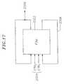
- FIG. 17is the FSM of the MCPE configuration controller of one embodiment.
- control information 2004is received by the FSM 2002 in the form of state information from at least one surrounding MCPE in the networked array.
- This control informationis in the form of two bits received from the Control Reduce block of the MCPE control logic structure.
- the FSMalso has three state bits that directly control the major and minor configuration contexts for the particular MCPE.
- the FSMmaintains the data of the current MCPE configuration by using a feedback path 2006 to feed back the current configuration state of the MCPE of the most recent clock cycle.
- the feedback path 2006is not limited to a single path.
- the FSMselects one of the available configuration memory contexts for use by the corresponding MCPE during the next clock cycle in response to the received state information from the surrounding MCPEs and the current configuration data. This selection is output from the FSM in the form of a configuration control signal 2008 .
- the selection of a configuration memory context for use during the next clock cycleoccurs, in one embodiment, during the execution of the configuration memory context selected for the current clock cycle.
- FIG. 18is a flowchart for manipulating a networked array of MCPEs in one embodiment.
- Each MCPE of the networked arrayis assigned a physical identification which, in one embodiment, is assigned at the time of network development. This physical identification may be based on the MCPE's physical location in the networked array.
- Operationbegins at block 1402 , at which a virtual identification is assigned to each of the MCPEs of the array.
- the physical identificationis used to address the MCPEs for reprogramming of the virtual identification because the physical identification is accessible to the programmer.
- the assigned virtual identificationmay be initialized to be the same as the physical identification.
- Datais transmitted to the MCPE array using the broadcast, or configuration, network, at block 1404 .
- the transmitted datacomprises an address mask, a destination identification, MCPE configuration data, and MCPE control data.
- the transmitted dataalso may be used in selecting between the use of the physical identification and the virtual identification in selecting MCPEs for manipulation. Furthermore, the transmitted data may be used to change the virtual identification of the MCPEs.
- the transmitted datain one embodiment is transmitted from another MCPE. In an alternate embodiment, the transmitted data is transmitted from an input/output device. In another alternate embodiment, the transmitted data is transmitted from an MCPE configuration controller. The transmitted data may also be transmitted from multiple sources at the same time.
- the address maskis applied, at block 1408 , to the virtual identification of each MCPE and to the transmitted destination identification.
- the masked virtual identification of each MCPEis compared to the masked destination identification, at block 1410 , using a comparison circuit.
- the MCPEis manipulated in response to the transmitted data, at block 1414 .
- the manipulationis performed using a manipulation circuit.
- the MCPEis not manipulated in response to transmitted data, at block 1416 .
- a MCPEcomprises the comparison circuit and the manipulation circuit.
- FIG. 19shows the selection of MCPEs using an address mask in one embodiment.
- the selection of MCPEs for configuration and controlis determined by applying a transmitted mask to either the physical address 1570 or the virtual address 1572 of the MCPEs 1550 - 1558 .
- the masked addressis then compared to a masked destination identification.
- MCPEs 1550 - 1558have physical addresses 0 - 8 , respectively.
- MCPE 1550has virtual address 0000 .
- MCPE 1551has virtual address 0001 .
- MCPE 1552has virtual address 0010 .
- MCPE 1553has virtual address 0100 .
- MCPE 1554has virtual address 0101 .
- MCPE 1555has virtual address 0110 .
- MCPE 1556has virtual address 1000 .
- MCPE 1557has virtual address 1100 .
- MCPE 1558has virtual address 1110 .
- the virtual address 1572will be used to select the MCPEs, so the mask will be applied to the virtual address 1572 .
- the maskis used to identify the significant bits of the virtual address 1572 that are to be compared against the significant bits of the masked destination identification in selecting the MCPEs.
- mask ( 0011 )When mask ( 0011 ) is transmitted, the third and fourth bits of the virtual address 1572 are identified as significant by this mask. This mask also identifies the third and fourth bits of the destination identification as significant. Therefore, any MCPE having the third and fourth bits of the virtual address matching the third and fourth bits of the destination identification is selected.
- MCPEs 1550 , 1553 , 1556 , and 1557are selected.
- MCPEs 1550 , 1553 , 1556 , and 1557define a region 1560 and execute a particular function within the networked array 1500 .
- manipulation of the selected MCPEsmay comprise programming the selected MCPEs with a number of configuration memory contexts. This programming may be accomplished simultaneously with the execution of a present function by the MCPE to be programmed.
- a first group of MCPEs located in a particular region of the chipmay be selectively programmed with a first configuration while other groups of MCPEs located in different regions of the same chip may be selectively programmed with configurations that are different from the first configuration and different from each other.
- the groups of MCPEs of the different regionsmay function independently of each other in one embodiment, and different regions may overlap in that multiple regions may use the same MCPEs.
- the groups of MCPEshave arbitrary shapes as defined by the physical location of the particular MCPEs required to carry out a function.
- manipulation of the selected MCPEscomprises selecting MCPE configuration memory contexts to control the functioning of the MCPEs.
- MCPE configuration memory contextsAs the address masking selection scheme results in the selection of different MCPEs or groups of MCPEs in different regions of a chip, then a first group of MCPEs located in a particular area of the chip may have a first configuration memory context selected while other groups of MCPEs located in different areas of the same chip may have configuration memory contexts selected that are different from the first configuration memory context and different from each other.
- manipulation of the selected MCPEsmay comprise programming the selected MCPEs of one region of the networked array with one group of configuration memory contexts. Moreover, the manipulation of the selected MCPEs also comprises selecting a different group of configuration memory contexts to control the functioning of other groups of MCPEs located in different areas of the same chip. The regions defined by the different groups of MCPEs may overlap in one embodiment.
- FIGS. 20-23illustrate the use of the address masking selection scheme in the selection and reconfiguration of different MCPEs or groups of MCPEs in different regions of a chip to perform different functions in one embodiment.
- An embodiment of the present inventioncan be configured in one of these illustrated configurations, but is not so limited to these configurations.
- a different configurationmay be selected for each MCPE on each different clock cycle.
- FIG. 20illustrates an 8-bit processor configuration of a reconfigurable processing device which has been constructed and programmed according to one embodiment.
- the two dimensional array of MCPEs 1900are located in a programmable interconnect 1901 .
- Five of the MCPEs 1911 - 1915 and the portion of the reconfigurable interconnect connecting the MCPEshave been configured to operate as an 8-bit microprocessor 1902 .
- One of the MCPEs 1914 denoted ALUutilizes logic resources to perform the logic operations of the 8-bit microprocessor 1902 and utilizes memory resources as a data store and/or extended register file.
- Another MCPE 1912operates as a function store that controls the successive logic operations performed by the logic resources of the ALU.
- Two additional MCPEs 1913 and 1915operate as further instruction stores that control the addressing of the memory resources of the ALU.
- a final MCPE 1911operates as a program counter for the various instruction MCPEs 1912 , 1913 , and 1915 .
- FIG. 21illustrates a single instruction multiple data system configuration of a reconfigurable processing device of one embodiment.
- the functions of the program counter 1602 and instruction stores 1604 , 1608 and 1610have been assigned to different MCPEs, but the ALU function has been replicated into 12 MCPEs.
- Each of the ALUsis connected via the reconfigurable interconnect 1601 to operate on globally broadcast instructions from the instruction stores 1604 , 1608 , and 1610 . These same operations are performed by each of these ALUs or common instructions may be broadcast on a row-by-row basis.
- FIG. 22illustrates a 32-bit processor configuration of a reconfigurable processing device which has been constructed and programmed according to one embodiment. This configuration allows for wider data paths in a processing device.
- This 32-bit microprocessor configured devicehas instruction stores 1702 , 1704 , and 1706 and a program counter 1708 .
- Four MCPEs 1710 - 1716have been assigned an ALU operation, and the ALUs are chained together to act as a single 32-bit wide microprocessor in which the interconnect 1701 supports carry in and carry out operations between the ALUs.
- FIG. 23illustrates a multiple instruction multiple data system configuration of a reconfigurable processing device of one embodiment.
- the 8-bit microprocessor configuration 1802 of FIG. 20is replicated into an adjacent set of MCPEs 1804 to accommodate multiple independent processing units within the same device. Furthermore, wider data paths could also be accommodated by chaining the ALUs 1806 and 1808 of each processor 1802 and 1804 , respectively, together.
Landscapes
- Engineering & Computer Science (AREA)
- Computer Hardware Design (AREA)
- Theoretical Computer Science (AREA)
- Computing Systems (AREA)
- Physics & Mathematics (AREA)
- General Engineering & Computer Science (AREA)
- General Physics & Mathematics (AREA)
- Logic Circuits (AREA)
Abstract
Description
Claims (21)
Priority Applications (2)
| Application Number | Priority Date | Filing Date | Title |
|---|---|---|---|
| US09/504,203US6526498B1 (en) | 1997-10-31 | 2000-02-15 | Method and apparatus for retiming in a network of multiple context processing elements |
| US10/320,018US7266672B2 (en) | 1997-10-31 | 2002-12-16 | Method and apparatus for retiming in a network of multiple context processing elements |
Applications Claiming Priority (2)
| Application Number | Priority Date | Filing Date | Title |
|---|---|---|---|
| US08/962,526US6122719A (en) | 1997-10-31 | 1997-10-31 | Method and apparatus for retiming in a network of multiple context processing elements |
| US09/504,203US6526498B1 (en) | 1997-10-31 | 2000-02-15 | Method and apparatus for retiming in a network of multiple context processing elements |
Related Parent Applications (1)
| Application Number | Title | Priority Date | Filing Date |
|---|---|---|---|
| US08/962,526ContinuationUS6122719A (en) | 1997-10-31 | 1997-10-31 | Method and apparatus for retiming in a network of multiple context processing elements |
Related Child Applications (1)
| Application Number | Title | Priority Date | Filing Date |
|---|---|---|---|
| US10/320,018ContinuationUS7266672B2 (en) | 1997-10-31 | 2002-12-16 | Method and apparatus for retiming in a network of multiple context processing elements |
Publications (1)
| Publication Number | Publication Date |
|---|---|
| US6526498B1true US6526498B1 (en) | 2003-02-25 |
Family
ID=25506014
Family Applications (3)
| Application Number | Title | Priority Date | Filing Date |
|---|---|---|---|
| US08/962,526Expired - LifetimeUS6122719A (en) | 1997-10-31 | 1997-10-31 | Method and apparatus for retiming in a network of multiple context processing elements |
| US09/504,203Expired - Fee RelatedUS6526498B1 (en) | 1997-10-31 | 2000-02-15 | Method and apparatus for retiming in a network of multiple context processing elements |
| US10/320,018Expired - Fee RelatedUS7266672B2 (en) | 1997-10-31 | 2002-12-16 | Method and apparatus for retiming in a network of multiple context processing elements |
Family Applications Before (1)
| Application Number | Title | Priority Date | Filing Date |
|---|---|---|---|
| US08/962,526Expired - LifetimeUS6122719A (en) | 1997-10-31 | 1997-10-31 | Method and apparatus for retiming in a network of multiple context processing elements |
Family Applications After (1)
| Application Number | Title | Priority Date | Filing Date |
|---|---|---|---|
| US10/320,018Expired - Fee RelatedUS7266672B2 (en) | 1997-10-31 | 2002-12-16 | Method and apparatus for retiming in a network of multiple context processing elements |
Country Status (1)
| Country | Link |
|---|---|
| US (3) | US6122719A (en) |
Cited By (26)
| Publication number | Priority date | Publication date | Assignee | Title |
|---|---|---|---|---|
| US20030126403A1 (en)* | 1997-10-31 | 2003-07-03 | Broadcom Corporation | Method and apparatus for retiming in a network of multiple context processing elements |
| US20040024959A1 (en)* | 2002-08-02 | 2004-02-05 | Taylor George R. | System and method for optically interconnecting memory devices |
| US20040024978A1 (en)* | 2002-08-05 | 2004-02-05 | Jeddeloh Joseph M. | Memory hub and access method having internal row caching |
| US20040028412A1 (en)* | 2002-08-09 | 2004-02-12 | Tim Murphy | System and method for multiple bit optical data transmission in memory systems |
| US20040034753A1 (en)* | 2002-08-16 | 2004-02-19 | Jeddeloh Joseph M. | Memory hub bypass circuit and method |
| US20040047169A1 (en)* | 2002-09-09 | 2004-03-11 | Lee Terry R. | Wavelength division multiplexed memory module, memory system and method |
| US20040250360A1 (en)* | 2003-06-16 | 2004-12-16 | Young Carl R. | Portable unloading dock |
| US20040260957A1 (en)* | 2003-06-20 | 2004-12-23 | Jeddeloh Joseph M. | System and method for selective memory module power management |
| US20040260891A1 (en)* | 2003-06-20 | 2004-12-23 | Jeddeloh Joseph M. | Posted write buffers and methods of posting write requests in memory modules |
| US20040260909A1 (en)* | 2003-06-20 | 2004-12-23 | Lee Terry R. | Memory hub and access method having internal prefetch buffers |
| US20050030797A1 (en)* | 2003-06-11 | 2005-02-10 | Pax George E. | Memory module and method having improved signal routing topology |
| US20050172183A1 (en)* | 2004-02-04 | 2005-08-04 | International Business Machines Corporation | Method and system for broadcasting data to multiple tap controllers |
| US20050210216A1 (en)* | 2004-03-08 | 2005-09-22 | Jobs Jeffrey R | Memory hub architecture having programmable lane widths |
| US20050216648A1 (en)* | 2004-03-25 | 2005-09-29 | Jeddeloh Joseph M | System and method for memory hub-based expansion bus |
| US20050228939A1 (en)* | 2004-04-08 | 2005-10-13 | Janzen Jeffery W | System and method for optimizing interconnections of components in a multichip memory module |
| US20050257021A1 (en)* | 2004-05-17 | 2005-11-17 | Ralph James | System and method for communicating the synchronization status of memory modules during initialization of the memory modules |
| US20050257024A1 (en)* | 2002-07-01 | 2005-11-17 | Elixent, Limited | Loosely-biased heterogeneous reconfigurable arrays |
| US20060206667A1 (en)* | 2002-08-29 | 2006-09-14 | Ryan Kevin J | System and method for optimizing interconnections of memory devices in a multichip module |
| US7120743B2 (en) | 2003-10-20 | 2006-10-10 | Micron Technology, Inc. | Arbitration system and method for memory responses in a hub-based memory system |
| US7120727B2 (en) | 2003-06-19 | 2006-10-10 | Micron Technology, Inc. | Reconfigurable memory module and method |
| US20060271720A1 (en)* | 2004-08-31 | 2006-11-30 | Ralph James | System and method for transmitting data packets in a computer system having a memory hub architecture |
| US7181584B2 (en) | 2004-02-05 | 2007-02-20 | Micron Technology, Inc. | Dynamic command and/or address mirroring system and method for memory modules |
| US7234070B2 (en) | 2003-10-27 | 2007-06-19 | Micron Technology, Inc. | System and method for using a learning sequence to establish communications on a high-speed nonsynchronous interface in the absence of clock forwarding |
| US20070156906A1 (en)* | 2000-10-27 | 2007-07-05 | Dowling Eric M | Negotiated wireless peripheral security systems |
| US20070168712A1 (en)* | 2005-11-18 | 2007-07-19 | Racunas Paul B | Method and apparatus for lockstep processing on a fixed-latency interconnect |
| US20090313435A1 (en)* | 2008-06-13 | 2009-12-17 | Hariharan Thantry | Optimizing concurrent accesses in a directory-based coherency protocol |
Families Citing this family (68)
| Publication number | Priority date | Publication date | Assignee | Title |
|---|---|---|---|---|
| US5943242A (en) | 1995-11-17 | 1999-08-24 | Pact Gmbh | Dynamically reconfigurable data processing system |
| US7266725B2 (en) | 2001-09-03 | 2007-09-04 | Pact Xpp Technologies Ag | Method for debugging reconfigurable architectures |
| US5956518A (en)* | 1996-04-11 | 1999-09-21 | Massachusetts Institute Of Technology | Intermediate-grain reconfigurable processing device |
| DE19651075A1 (en) | 1996-12-09 | 1998-06-10 | Pact Inf Tech Gmbh | Unit for processing numerical and logical operations, for use in processors (CPU's), multi-computer systems, data flow processors (DFP's), digital signal processors (DSP's) or the like |
| DE19654595A1 (en) | 1996-12-20 | 1998-07-02 | Pact Inf Tech Gmbh | I0 and memory bus system for DFPs as well as building blocks with two- or multi-dimensional programmable cell structures |
| DE19654593A1 (en) | 1996-12-20 | 1998-07-02 | Pact Inf Tech Gmbh | Reconfiguration procedure for programmable blocks at runtime |
| US6338106B1 (en) | 1996-12-20 | 2002-01-08 | Pact Gmbh | I/O and memory bus system for DFPS and units with two or multi-dimensional programmable cell architectures |
| DE19654846A1 (en) | 1996-12-27 | 1998-07-09 | Pact Inf Tech Gmbh | Process for the independent dynamic reloading of data flow processors (DFPs) as well as modules with two- or multi-dimensional programmable cell structures (FPGAs, DPGAs, etc.) |
| ATE243390T1 (en) | 1996-12-27 | 2003-07-15 | Pact Inf Tech Gmbh | METHOD FOR INDEPENDENT DYNAMIC LOADING OF DATA FLOW PROCESSORS (DFPS) AND COMPONENTS WITH TWO- OR MULTI-DIMENSIONAL PROGRAMMABLE CELL STRUCTURES (FPGAS, DPGAS, O.L.) |
| DE19704728A1 (en) | 1997-02-08 | 1998-08-13 | Pact Inf Tech Gmbh | Method for self-synchronization of configurable elements of a programmable module |
| US6542998B1 (en) | 1997-02-08 | 2003-04-01 | Pact Gmbh | Method of self-synchronization of configurable elements of a programmable module |
| DE19704742A1 (en) | 1997-02-11 | 1998-09-24 | Pact Inf Tech Gmbh | Internal bus system for DFPs, as well as modules with two- or multi-dimensional programmable cell structures, for coping with large amounts of data with high networking effort |
| US8686549B2 (en) | 2001-09-03 | 2014-04-01 | Martin Vorbach | Reconfigurable elements |
| DE19861088A1 (en) | 1997-12-22 | 2000-02-10 | Pact Inf Tech Gmbh | Repairing integrated circuits by replacing subassemblies with substitutes |
| DE19807872A1 (en) | 1998-02-25 | 1999-08-26 | Pact Inf Tech Gmbh | Method of managing configuration data in data flow processors |
| WO2000077652A2 (en) | 1999-06-10 | 2000-12-21 | Pact Informationstechnologie Gmbh | Sequence partitioning in cell structures |
| US6763375B1 (en)* | 2000-04-11 | 2004-07-13 | International Business Machines Corporation | Method for defining and controlling the overall behavior of a network processor device |
| EP2226732A3 (en) | 2000-06-13 | 2016-04-06 | PACT XPP Technologies AG | Cache hierarchy for a multicore processor |
| US6675289B1 (en) | 2000-06-30 | 2004-01-06 | Broadcom Corporation | System and method for executing hybridized code on a dynamically configurable hardware environment |
| US7249351B1 (en) | 2000-08-30 | 2007-07-24 | Broadcom Corporation | System and method for preparing software for execution in a dynamically configurable hardware environment |
| WO2002021323A2 (en)* | 2000-09-08 | 2002-03-14 | Avaz Networks | Hardware function generator support in a dsp |
| US8058899B2 (en) | 2000-10-06 | 2011-11-15 | Martin Vorbach | Logic cell array and bus system |
| AU2060002A (en) | 2000-10-06 | 2002-04-22 | Pact Inf Tech Gmbh | Method and device |
| US6990555B2 (en)* | 2001-01-09 | 2006-01-24 | Pact Xpp Technologies Ag | Method of hierarchical caching of configuration data having dataflow processors and modules having two- or multidimensional programmable cell structure (FPGAs, DPGAs, etc.) |
| US7089436B2 (en)* | 2001-02-05 | 2006-08-08 | Morpho Technologies | Power saving method and arrangement for a configurable processor array |
| US7210129B2 (en)* | 2001-08-16 | 2007-04-24 | Pact Xpp Technologies Ag | Method for translating programs for reconfigurable architectures |
| US9250908B2 (en) | 2001-03-05 | 2016-02-02 | Pact Xpp Technologies Ag | Multi-processor bus and cache interconnection system |
| US9436631B2 (en) | 2001-03-05 | 2016-09-06 | Pact Xpp Technologies Ag | Chip including memory element storing higher level memory data on a page by page basis |
| US9411532B2 (en) | 2001-09-07 | 2016-08-09 | Pact Xpp Technologies Ag | Methods and systems for transferring data between a processing device and external devices |
| US9552047B2 (en) | 2001-03-05 | 2017-01-24 | Pact Xpp Technologies Ag | Multiprocessor having runtime adjustable clock and clock dependent power supply |
| US9037807B2 (en) | 2001-03-05 | 2015-05-19 | Pact Xpp Technologies Ag | Processor arrangement on a chip including data processing, memory, and interface elements |
| US7581076B2 (en) | 2001-03-05 | 2009-08-25 | Pact Xpp Technologies Ag | Methods and devices for treating and/or processing data |
| US7444531B2 (en) | 2001-03-05 | 2008-10-28 | Pact Xpp Technologies Ag | Methods and devices for treating and processing data |
| US7844796B2 (en) | 2001-03-05 | 2010-11-30 | Martin Vorbach | Data processing device and method |
| US20030088757A1 (en)* | 2001-05-02 | 2003-05-08 | Joshua Lindner | Efficient high performance data operation element for use in a reconfigurable logic environment |
| TWI234737B (en)* | 2001-05-24 | 2005-06-21 | Ip Flex Inc | Integrated circuit device |
| AU2002347560A1 (en) | 2001-06-20 | 2003-01-02 | Pact Xpp Technologies Ag | Data processing method |
| US10031733B2 (en) | 2001-06-20 | 2018-07-24 | Scientia Sol Mentis Ag | Method for processing data |
| US7996827B2 (en) | 2001-08-16 | 2011-08-09 | Martin Vorbach | Method for the translation of programs for reconfigurable architectures |
| US7434191B2 (en) | 2001-09-03 | 2008-10-07 | Pact Xpp Technologies Ag | Router |
| CN100397331C (en)* | 2001-09-07 | 2008-06-25 | Ip菲力股份有限公司 | Data processing system and control method thereof |
| US8686475B2 (en) | 2001-09-19 | 2014-04-01 | Pact Xpp Technologies Ag | Reconfigurable elements |
| US20030105799A1 (en)* | 2001-12-03 | 2003-06-05 | Avaz Networks, Inc. | Distributed processing architecture with scalable processing layers |
| US20030112758A1 (en)* | 2001-12-03 | 2003-06-19 | Pang Jon Laurent | Methods and systems for managing variable delays in packet transmission |
| US7577822B2 (en) | 2001-12-14 | 2009-08-18 | Pact Xpp Technologies Ag | Parallel task operation in processor and reconfigurable coprocessor configured based on information in link list including termination information for synchronization |
| GB2383240B (en)* | 2001-12-17 | 2005-02-16 | Micron Technology Inc | DVi link with parallel test data |
| DE10392560D2 (en) | 2002-01-19 | 2005-05-12 | Pact Xpp Technologies Ag | Reconfigurable processor |
| US8127061B2 (en) | 2002-02-18 | 2012-02-28 | Martin Vorbach | Bus systems and reconfiguration methods |
| US8914590B2 (en) | 2002-08-07 | 2014-12-16 | Pact Xpp Technologies Ag | Data processing method and device |
| US9170812B2 (en) | 2002-03-21 | 2015-10-27 | Pact Xpp Technologies Ag | Data processing system having integrated pipelined array data processor |
| US7620678B1 (en)* | 2002-06-12 | 2009-11-17 | Nvidia Corporation | Method and system for reducing the time-to-market concerns for embedded system design |
| AU2003286131A1 (en) | 2002-08-07 | 2004-03-19 | Pact Xpp Technologies Ag | Method and device for processing data |
| US7657861B2 (en) | 2002-08-07 | 2010-02-02 | Pact Xpp Technologies Ag | Method and device for processing data |
| US7394284B2 (en) | 2002-09-06 | 2008-07-01 | Pact Xpp Technologies Ag | Reconfigurable sequencer structure |
| JP2006510129A (en)* | 2002-12-12 | 2006-03-23 | コーニンクレッカ フィリップス エレクトロニクス エヌ ヴィ | Modular integration of array processor into system on chip |
| EP1676208A2 (en) | 2003-08-28 | 2006-07-05 | PACT XPP Technologies AG | Data processing device and method |
| JP4502650B2 (en)* | 2004-02-03 | 2010-07-14 | 日本電気株式会社 | Array type processor |
| CA2593247A1 (en)* | 2005-01-10 | 2006-11-16 | Quartics, Inc. | Integrated architecture for the unified processing of visual media |
| KR100730280B1 (en)* | 2005-12-06 | 2007-06-19 | 삼성전자주식회사 | Apparatus and Method for Optimizing Loop Buffer in Reconstruction Processor |
| JP2009524134A (en) | 2006-01-18 | 2009-06-25 | ペーアーツェーテー イクスペーペー テクノロジーズ アクチエンゲゼルシャフト | Hardware definition method |
| JP4782591B2 (en)* | 2006-03-10 | 2011-09-28 | 富士通セミコンダクター株式会社 | Reconfigurable circuit |
| KR100781340B1 (en)* | 2006-09-18 | 2007-11-30 | 삼성전자주식회사 | Computation system and method for handling user-defined extended operations |
| US20080212890A1 (en)* | 2007-01-10 | 2008-09-04 | Loubachevskaia Natalya Y | Systems and Methods for Noise Estimation in a Single Frame of Video Data |
| US20090201989A1 (en)* | 2007-11-01 | 2009-08-13 | Sherjil Ahmed | Systems and Methods to Optimize Entropy Decoding |
| JP4962305B2 (en)* | 2007-12-26 | 2012-06-27 | 富士通セミコンダクター株式会社 | Reconfigurable circuit |
| JP5599987B2 (en)* | 2009-06-12 | 2014-10-01 | スパンション エルエルシー | Auxiliary PE for multiplexing and semiconductor integrated circuit |
| US12072835B2 (en)* | 2022-06-28 | 2024-08-27 | Intel Corporation | Multicore synchronization mechanism for time critical radio systems |
| US12236241B2 (en)* | 2023-02-24 | 2025-02-25 | Arm Limited | Data processing apparatus with selectively delayed transmission of operands |
Citations (25)
| Publication number | Priority date | Publication date | Assignee | Title |
|---|---|---|---|---|
| US4597041A (en) | 1982-11-15 | 1986-06-24 | Data General Corp. | Method and apparatus for enhancing the operation of a data processing system |
| US4748585A (en) | 1985-12-26 | 1988-05-31 | Chiarulli Donald M | Processor utilizing reconfigurable process segments to accomodate data word length |
| US4754412A (en) | 1985-10-07 | 1988-06-28 | Schlumberger Systems & Services, Inc. | Arithmetic logic system using the output of a first alu to control the operation of a second alu |
| US4858113A (en) | 1987-04-10 | 1989-08-15 | The United States Of America As Represented By The Director Of The National Security Agency | Reconfigurable pipelined processor |
| US4870302A (en) | 1984-03-12 | 1989-09-26 | Xilinx, Inc. | Configurable electrical circuit having configurable logic elements and configurable interconnects |
| US4967340A (en)* | 1985-06-12 | 1990-10-30 | E-Systems, Inc. | Adaptive processing system having an array of individually configurable processing components |
| US5020059A (en) | 1989-03-31 | 1991-05-28 | At&T Bell Laboratories | Reconfigurable signal processor |
| US5081575A (en) | 1987-11-06 | 1992-01-14 | Oryx Corporation | Highly parallel computer architecture employing crossbar switch with selectable pipeline delay |
| US5233539A (en) | 1989-08-15 | 1993-08-03 | Advanced Micro Devices, Inc. | Programmable gate array with improved interconnect structure, input/output structure and configurable logic block |
| US5301340A (en) | 1990-10-31 | 1994-04-05 | International Business Machines Corporation | IC chips including ALUs and identical register files whereby a number of ALUs directly and concurrently write results to every register file per cycle |
| US5317209A (en)* | 1991-08-29 | 1994-05-31 | National Semiconductor Corporation | Dynamic three-state bussing capability in a configurable logic array |
| US5317755A (en) | 1991-04-10 | 1994-05-31 | General Electric Company | Systolic array processors for reducing under-utilization of original design parallel-bit processors with digit-serial processors by using maximum common divisor of latency around the loop connection |
| US5426378A (en) | 1994-04-20 | 1995-06-20 | Xilinx, Inc. | Programmable logic device which stores more than one configuration and means for switching configurations |
| US5457408A (en) | 1994-11-23 | 1995-10-10 | At&T Corp. | Method and apparatus for verifying whether a bitstream received by a field programmable gate array (FPGA) is intended for that FPGA |
| US5469003A (en) | 1992-11-05 | 1995-11-21 | Xilinx, Inc. | Hierarchically connectable configurable cellular array |
| US5581199A (en)* | 1995-01-04 | 1996-12-03 | Xilinx, Inc. | Interconnect architecture for field programmable gate array using variable length conductors |
| US5684980A (en) | 1992-07-29 | 1997-11-04 | Virtual Computer Corporation | FPGA virtual computer for executing a sequence of program instructions by successively reconfiguring a group of FPGA in response to those instructions |
| US5694070A (en)* | 1994-07-11 | 1997-12-02 | Vitesse Semiconductor Corporation | Distributed ramp delay generator |
| US5727021A (en)* | 1996-04-03 | 1998-03-10 | Teradyne, Inc. | Apparatus and method for providing a programmable delay with low fixed delay |
| US5742180A (en) | 1995-02-10 | 1998-04-21 | Massachusetts Institute Of Technology | Dynamically programmable gate array with multiple contexts |
| US5754818A (en) | 1996-03-22 | 1998-05-19 | Sun Microsystems, Inc. | Architecture and method for sharing TLB entries through process IDS |
| US5765209A (en) | 1993-09-23 | 1998-06-09 | Hewlett-Packard Co. | Method and apparatus to eliminate redundant mapping in a TLB utilizing variable sized pages |
| US5778439A (en) | 1995-08-18 | 1998-07-07 | Xilinx, Inc. | Programmable logic device with hierarchical confiquration and state storage |
| US5880598A (en)* | 1997-01-10 | 1999-03-09 | Xilinx, Inc. | Tile-based modular routing resources for high density programmable logic device |
| US5956518A (en) | 1996-04-11 | 1999-09-21 | Massachusetts Institute Of Technology | Intermediate-grain reconfigurable processing device |
Family Cites Families (8)
| Publication number | Priority date | Publication date | Assignee | Title |
|---|---|---|---|---|
| US4625290A (en)* | 1983-11-02 | 1986-11-25 | University Of Florida | Apparatus and method for producing a three-dimensional display on a video display device |
| US5142677A (en)* | 1989-05-04 | 1992-08-25 | Texas Instruments Incorporated | Context switching devices, systems and methods |
| IL98248A0 (en)* | 1991-05-23 | 1992-06-21 | Ibm Israel | Instruction scheduler for a computer |
| US5550540A (en)* | 1992-11-12 | 1996-08-27 | Internatioal Business Machines Corporation | Distributed coding and prediction by use of contexts |
| GB2293468B (en)* | 1994-09-21 | 1999-09-29 | Sony Uk Ltd | Data processing systems |
| JPH0954761A (en)* | 1995-08-15 | 1997-02-25 | Sony Corp | Digital signal processor and information processing system |
| US5692165A (en)* | 1995-09-12 | 1997-11-25 | Micron Electronics Inc. | Memory controller with low skew control signal |
| US6122719A (en)* | 1997-10-31 | 2000-09-19 | Silicon Spice | Method and apparatus for retiming in a network of multiple context processing elements |
- 1997
- 1997-10-31USUS08/962,526patent/US6122719A/ennot_activeExpired - Lifetime
- 2000
- 2000-02-15USUS09/504,203patent/US6526498B1/ennot_activeExpired - Fee Related
- 2002
- 2002-12-16USUS10/320,018patent/US7266672B2/ennot_activeExpired - Fee Related
Patent Citations (26)
| Publication number | Priority date | Publication date | Assignee | Title |
|---|---|---|---|---|
| US4597041A (en) | 1982-11-15 | 1986-06-24 | Data General Corp. | Method and apparatus for enhancing the operation of a data processing system |
| US4870302A (en) | 1984-03-12 | 1989-09-26 | Xilinx, Inc. | Configurable electrical circuit having configurable logic elements and configurable interconnects |
| US4967340A (en)* | 1985-06-12 | 1990-10-30 | E-Systems, Inc. | Adaptive processing system having an array of individually configurable processing components |
| US4754412A (en) | 1985-10-07 | 1988-06-28 | Schlumberger Systems & Services, Inc. | Arithmetic logic system using the output of a first alu to control the operation of a second alu |
| US4748585A (en) | 1985-12-26 | 1988-05-31 | Chiarulli Donald M | Processor utilizing reconfigurable process segments to accomodate data word length |
| US4858113A (en) | 1987-04-10 | 1989-08-15 | The United States Of America As Represented By The Director Of The National Security Agency | Reconfigurable pipelined processor |
| US5081575A (en) | 1987-11-06 | 1992-01-14 | Oryx Corporation | Highly parallel computer architecture employing crossbar switch with selectable pipeline delay |
| US5020059A (en) | 1989-03-31 | 1991-05-28 | At&T Bell Laboratories | Reconfigurable signal processor |
| US5233539A (en) | 1989-08-15 | 1993-08-03 | Advanced Micro Devices, Inc. | Programmable gate array with improved interconnect structure, input/output structure and configurable logic block |
| US5301340A (en) | 1990-10-31 | 1994-04-05 | International Business Machines Corporation | IC chips including ALUs and identical register files whereby a number of ALUs directly and concurrently write results to every register file per cycle |
| US5317755A (en) | 1991-04-10 | 1994-05-31 | General Electric Company | Systolic array processors for reducing under-utilization of original design parallel-bit processors with digit-serial processors by using maximum common divisor of latency around the loop connection |
| US5336950A (en) | 1991-08-29 | 1994-08-09 | National Semiconductor Corporation | Configuration features in a configurable logic array |
| US5317209A (en)* | 1991-08-29 | 1994-05-31 | National Semiconductor Corporation | Dynamic three-state bussing capability in a configurable logic array |
| US5684980A (en) | 1992-07-29 | 1997-11-04 | Virtual Computer Corporation | FPGA virtual computer for executing a sequence of program instructions by successively reconfiguring a group of FPGA in response to those instructions |
| US5469003A (en) | 1992-11-05 | 1995-11-21 | Xilinx, Inc. | Hierarchically connectable configurable cellular array |
| US5765209A (en) | 1993-09-23 | 1998-06-09 | Hewlett-Packard Co. | Method and apparatus to eliminate redundant mapping in a TLB utilizing variable sized pages |
| US5426378A (en) | 1994-04-20 | 1995-06-20 | Xilinx, Inc. | Programmable logic device which stores more than one configuration and means for switching configurations |
| US5694070A (en)* | 1994-07-11 | 1997-12-02 | Vitesse Semiconductor Corporation | Distributed ramp delay generator |
| US5457408A (en) | 1994-11-23 | 1995-10-10 | At&T Corp. | Method and apparatus for verifying whether a bitstream received by a field programmable gate array (FPGA) is intended for that FPGA |
| US5581199A (en)* | 1995-01-04 | 1996-12-03 | Xilinx, Inc. | Interconnect architecture for field programmable gate array using variable length conductors |
| US5742180A (en) | 1995-02-10 | 1998-04-21 | Massachusetts Institute Of Technology | Dynamically programmable gate array with multiple contexts |
| US5778439A (en) | 1995-08-18 | 1998-07-07 | Xilinx, Inc. | Programmable logic device with hierarchical confiquration and state storage |
| US5754818A (en) | 1996-03-22 | 1998-05-19 | Sun Microsystems, Inc. | Architecture and method for sharing TLB entries through process IDS |
| US5727021A (en)* | 1996-04-03 | 1998-03-10 | Teradyne, Inc. | Apparatus and method for providing a programmable delay with low fixed delay |
| US5956518A (en) | 1996-04-11 | 1999-09-21 | Massachusetts Institute Of Technology | Intermediate-grain reconfigurable processing device |
| US5880598A (en)* | 1997-01-10 | 1999-03-09 | Xilinx, Inc. | Tile-based modular routing resources for high density programmable logic device |
Non-Patent Citations (24)
| Title |
|---|
| Alexander, et al., A Reconfigurable Approach to a Systolic Sorting Architecture, IEEE Feb. 1989, pp. 1178-1182. |
| Baker, "Programming silicon," Aug. 28, 1995, Electronic Engineering Times, p. 73. |
| Beal, et al., "Design of a Processor Element for a High Performance Massively Parallel SIMD System," Int'l Journal of High Speed Computing, vol. 7, No. 3, Sep. 1995, pp. 365-390. |
| Blazek, et al., "Design of a Reconfigurable Parallel RISC-Machine," North Holland Microprocessing and Microprogramming, 1987, pp. 39-46. |
| Bridges, "The CPA Machine: A Generally Partitionable MSIMD Architecture," IEEE Third Symposium on The Frontiers of Massively Parallel Computation, Feb. 1990, pps 196-203. |
| Brown, "Smart Compilers Puncture Code Bloat," Oct. 9, 1995, Electronic Engineering Times, pp. 38 and 42. |
| Carter, et al, "A User Programable Reconfigurable Logic Array," IEEE 1986 Custom Integrated Circuits Conference, pp. 233-235. |
| Clark, "Pilkington Preps Reconfigurable Video DSP," EE Times, week of Jul. 31, 1995. |
| Fiske, et al., "The Reconfigurable Arithmetic Processor," The 15th Annual International Symposium on Computer Architecture, May 30-Jun. 2, 1988, pp. 30-36. |
| Gray, et al., "Configurable Hardware: A New Paradigm for Computation," 1989, Massachusetts Institute of Technology, pp. 279-296. |
| Guo, et al., "A Novel Programmable Interconnect Architecture with Decoded Ram Storage," Proceedings of the IEEE Custom Integrated Circuits Conference, May 1-4, 1994, pps 193-196. |
| Hon, et al., "Reinventing Computing," Mar. 1996, MIT A1 Lab; p. 1. |
| Johnson, et al., "General-Purpose Systolic Arrays," IEEE Nov. 1993, pp. 20-31. |
| Masera, et al., "A Microprogrammable Parallel Architecture for DSP," Proceedings of the International Conference on Circuits and Systems, Jun. 1991, pp. 824-827. |
| Mirsky, Ethan A., "Coarse-Grain Reconfigurable Computing," Thesis submitted at the Massachusetts Institute of Technology, Jun. 1996. |
| Morton, et al., "The Dynamically Reconfigurable CAP Array Chip I," IEEE Journal of Solid-State Circuits, vol. SC-21, No. 5, Oct. 1986, pp. 820-826. |
| Razdan, et al., "A High-Performance Microarchitecture with Hardware-Progammable Functional Units," Micro-27 Proc. 27th Ann. Int'l Symposium on Microarchitecture, Nov. 30-Dec. 2 '94 pp 172-80. |
| Snyder, "An Inquiry into the Benefits of Multigauge Parallel Computation," Proceedings of the 1995 International Conference on Parallel Processing, Aug. 20-23, 1995, pp. 488-492. |
| Snyder. "A Taxonomy of Synchronous Parallel Machines," Proceedings of the 1988 International Conference on Parallel Processing, Aug. 15-19, 1998, pp. 281-285. |
| Sowa, et al., "Parallel Execution on the Function-Partitioned Processor with Multiple Instruction Streams," Systems and Computers in Japan, vol. 22, No. 4, 1991, pp. 22-27. |
| Valero-Garcia, et al., "Implementation of Systolic Algorithms Using Pipelined Functional Units," IEEE Proc. on the Int'l Conf. on Application Specific Array Processors, Sep. 5-7, '90, pps 273-283. |
| Vuillemin et al., "Programmable Active Memories: Reconfigurable Systems Come of Age," IEEE Transactions on VLSI Systems, 1995, pp. 1-15. |
| Wang, et al., "An Array Architecture for Reconfigurable Datapaths," More FPGA's, W.R. Moore & W. Luk; 1994 Abingdon EE&CD Books, pp. 35-46. |
| Xilinx Advance Product Information, "XC6200 Field Programmable Gate Arrays," Jan. 9, 1997 (Version 1.8), pp. 1-53. |
Cited By (110)
| Publication number | Priority date | Publication date | Assignee | Title |
|---|---|---|---|---|
| US20030126403A1 (en)* | 1997-10-31 | 2003-07-03 | Broadcom Corporation | Method and apparatus for retiming in a network of multiple context processing elements |
| US7266672B2 (en)* | 1997-10-31 | 2007-09-04 | Broadcom Corporation | Method and apparatus for retiming in a network of multiple context processing elements |
| US20070156906A1 (en)* | 2000-10-27 | 2007-07-05 | Dowling Eric M | Negotiated wireless peripheral security systems |
| US7461234B2 (en)* | 2002-07-01 | 2008-12-02 | Panasonic Corporation | Loosely-biased heterogeneous reconfigurable arrays |
| US20050257024A1 (en)* | 2002-07-01 | 2005-11-17 | Elixent, Limited | Loosely-biased heterogeneous reconfigurable arrays |
| US7411807B2 (en) | 2002-08-02 | 2008-08-12 | Micron Technology, Inc. | System and method for optically interconnecting memory devices |
| US20040024959A1 (en)* | 2002-08-02 | 2004-02-05 | Taylor George R. | System and method for optically interconnecting memory devices |
| US20070025133A1 (en)* | 2002-08-02 | 2007-02-01 | Taylor George R | System and method for optical interconnecting memory devices |
| US7382639B2 (en) | 2002-08-02 | 2008-06-03 | Micron Technology, Inc. | System and method for optically interconnecting memory devices |
| US20070035980A1 (en)* | 2002-08-02 | 2007-02-15 | Taylor George R | System and method for optically interconnecting memory devices |
| US7200024B2 (en) | 2002-08-02 | 2007-04-03 | Micron Technology, Inc. | System and method for optically interconnecting memory devices |
| US7289347B2 (en) | 2002-08-02 | 2007-10-30 | Micron Technology, Inc. | System and method for optically interconnecting memory devices |
| US20050146946A1 (en)* | 2002-08-02 | 2005-07-07 | Taylor George R. | System and method for optically interconnecting memory devices |
| US20040024978A1 (en)* | 2002-08-05 | 2004-02-05 | Jeddeloh Joseph M. | Memory hub and access method having internal row caching |
| US7117316B2 (en) | 2002-08-05 | 2006-10-03 | Micron Technology, Inc. | Memory hub and access method having internal row caching |
| US7489875B2 (en) | 2002-08-09 | 2009-02-10 | Micron Technology, Inc. | System and method for multiple bit optical data transmission in memory systems |
| US7254331B2 (en) | 2002-08-09 | 2007-08-07 | Micron Technology, Inc. | System and method for multiple bit optical data transmission in memory systems |
| US20040028412A1 (en)* | 2002-08-09 | 2004-02-12 | Tim Murphy | System and method for multiple bit optical data transmission in memory systems |
| US20060204247A1 (en)* | 2002-08-09 | 2006-09-14 | Tim Murphy | System and method for multiple bit optical data transmission in memory systems |
| US7415567B2 (en) | 2002-08-16 | 2008-08-19 | Micron Technology, Inc. | Memory hub bypass circuit and method |
| US20060174070A1 (en)* | 2002-08-16 | 2006-08-03 | Jeddeloh Joseph M | Memory hub bypass circuit and method |
| US20040034753A1 (en)* | 2002-08-16 | 2004-02-19 | Jeddeloh Joseph M. | Memory hub bypass circuit and method |
| US7149874B2 (en) | 2002-08-16 | 2006-12-12 | Micron Technology, Inc. | Memory hub bypass circuit and method |
| US20060206667A1 (en)* | 2002-08-29 | 2006-09-14 | Ryan Kevin J | System and method for optimizing interconnections of memory devices in a multichip module |
| US8190819B2 (en) | 2002-08-29 | 2012-05-29 | Micron Technology, Inc. | System and method for optimizing interconnections of memory devices in a multichip module |
| US7805586B2 (en) | 2002-08-29 | 2010-09-28 | Micron Technology, Inc. | System and method for optimizing interconnections of memory devices in a multichip module |
| US7836252B2 (en) | 2002-08-29 | 2010-11-16 | Micron Technology, Inc. | System and method for optimizing interconnections of memory devices in a multichip module |
| US20040257890A1 (en)* | 2002-09-09 | 2004-12-23 | Lee Terry R. | Wavelength division multiplexed memory module, memory system and method |
| US20040047169A1 (en)* | 2002-09-09 | 2004-03-11 | Lee Terry R. | Wavelength division multiplexed memory module, memory system and method |
| US7106611B2 (en) | 2002-09-09 | 2006-09-12 | Micron Technology, Inc. | Wavelength division multiplexed memory module, memory system and method |
| US7242213B2 (en)* | 2003-06-11 | 2007-07-10 | Micron Technology, Inc. | Memory module and method having improved signal routing topology |
| US7245145B2 (en) | 2003-06-11 | 2007-07-17 | Micron Technology, Inc. | Memory module and method having improved signal routing topology |
| US20080036492A1 (en)* | 2003-06-11 | 2008-02-14 | Micron Technology, Inc. | Memory module and method having improved signal routing topology |
| US20060023528A1 (en)* | 2003-06-11 | 2006-02-02 | Pax George E | Memory module and method having improved signal routing topology |
| US20050030797A1 (en)* | 2003-06-11 | 2005-02-10 | Pax George E. | Memory module and method having improved signal routing topology |
| US7282947B2 (en) | 2003-06-11 | 2007-10-16 | Micron Technology, Inc. | Memory module and method having improved signal routing topology |
| US20090243649A1 (en)* | 2003-06-11 | 2009-10-01 | Pax George E | Memory module and method having improved signal routing topology |
| US7557601B2 (en) | 2003-06-11 | 2009-07-07 | Micron Technology, Inc. | Memory module and method having improved signal routing topology |
| US7746095B2 (en) | 2003-06-11 | 2010-06-29 | Round Rock Research, Llc | Memory module and method having improved signal routing topology |
| US20040250360A1 (en)* | 2003-06-16 | 2004-12-16 | Young Carl R. | Portable unloading dock |
| US20080140952A1 (en)* | 2003-06-19 | 2008-06-12 | Micro Technology, Inc. | Reconfigurable memory module and method |
| US20070011392A1 (en)* | 2003-06-19 | 2007-01-11 | Lee Terry R | Reconfigurable memory module and method |
| US7966444B2 (en) | 2003-06-19 | 2011-06-21 | Round Rock Research, Llc | Reconfigurable memory module and method |
| US8732383B2 (en) | 2003-06-19 | 2014-05-20 | Round Rock Research, Llc | Reconfigurable memory module and method |
| US8200884B2 (en) | 2003-06-19 | 2012-06-12 | Round Rock Research, Llc | Reconfigurable memory module and method |
| US7818712B2 (en) | 2003-06-19 | 2010-10-19 | Round Rock Research, Llc | Reconfigurable memory module and method |
| US7120727B2 (en) | 2003-06-19 | 2006-10-10 | Micron Technology, Inc. | Reconfigurable memory module and method |
| US7107415B2 (en) | 2003-06-20 | 2006-09-12 | Micron Technology, Inc. | Posted write buffers and methods of posting write requests in memory modules |
| US7260685B2 (en) | 2003-06-20 | 2007-08-21 | Micron Technology, Inc. | Memory hub and access method having internal prefetch buffers |
| US7412566B2 (en) | 2003-06-20 | 2008-08-12 | Micron Technology, Inc. | Memory hub and access method having internal prefetch buffers |
| US8127081B2 (en) | 2003-06-20 | 2012-02-28 | Round Rock Research, Llc | Memory hub and access method having internal prefetch buffers |
| US7428644B2 (en) | 2003-06-20 | 2008-09-23 | Micron Technology, Inc. | System and method for selective memory module power management |
| US20040260957A1 (en)* | 2003-06-20 | 2004-12-23 | Jeddeloh Joseph M. | System and method for selective memory module power management |
| US7437579B2 (en) | 2003-06-20 | 2008-10-14 | Micron Technology, Inc. | System and method for selective memory module power management |
| US7529896B2 (en) | 2003-06-20 | 2009-05-05 | Micron Technology, Inc. | Memory modules having a memory hub containing a posted write buffer, a memory device interface and a link interface, and method of posting write requests in memory modules |
| US20040260891A1 (en)* | 2003-06-20 | 2004-12-23 | Jeddeloh Joseph M. | Posted write buffers and methods of posting write requests in memory modules |
| US20040260909A1 (en)* | 2003-06-20 | 2004-12-23 | Lee Terry R. | Memory hub and access method having internal prefetch buffers |
| US20060288172A1 (en)* | 2003-06-20 | 2006-12-21 | Lee Terry R | Memory hub and access method having internal prefetch buffers |
| US20060206738A1 (en)* | 2003-06-20 | 2006-09-14 | Jeddeloh Joseph M | System and method for selective memory module power management |
| US20060212655A1 (en)* | 2003-06-20 | 2006-09-21 | Jeddeloh Joseph M | Posted write buffers and method of posting write requests in memory modules |
| US20060271746A1 (en)* | 2003-10-20 | 2006-11-30 | Meyer James W | Arbitration system and method for memory responses in a hub-based memory system |
| US7120743B2 (en) | 2003-10-20 | 2006-10-10 | Micron Technology, Inc. | Arbitration system and method for memory responses in a hub-based memory system |
| US8589643B2 (en) | 2003-10-20 | 2013-11-19 | Round Rock Research, Llc | Arbitration system and method for memory responses in a hub-based memory system |
| US7461286B2 (en) | 2003-10-27 | 2008-12-02 | Micron Technology, Inc. | System and method for using a learning sequence to establish communications on a high-speed nonsynchronous interface in the absence of clock forwarding |
| US7234070B2 (en) | 2003-10-27 | 2007-06-19 | Micron Technology, Inc. | System and method for using a learning sequence to establish communications on a high-speed nonsynchronous interface in the absence of clock forwarding |
| US20050172183A1 (en)* | 2004-02-04 | 2005-08-04 | International Business Machines Corporation | Method and system for broadcasting data to multiple tap controllers |
| US7181661B2 (en) | 2004-02-04 | 2007-02-20 | International Business Machines Corporation | Method and system for broadcasting data to multiple tap controllers |
| US7546435B2 (en) | 2004-02-05 | 2009-06-09 | Micron Technology. Inc. | Dynamic command and/or address mirroring system and method for memory modules |
| US20070143553A1 (en)* | 2004-02-05 | 2007-06-21 | Micron Technology, Inc. | Dynamic command and/or address mirroring system and method for memory modules |
| US7181584B2 (en) | 2004-02-05 | 2007-02-20 | Micron Technology, Inc. | Dynamic command and/or address mirroring system and method for memory modules |
| US7596675B2 (en) | 2004-03-08 | 2009-09-29 | Micron Technology, Inc. | Memory hub architecture having programmable lane widths |
| US20090319750A1 (en)* | 2004-03-08 | 2009-12-24 | Micron Technology, Inc. | Memory hub architecture having programmable lane widths |
| US9274991B2 (en) | 2004-03-08 | 2016-03-01 | Micron Technology, Inc. | Memory hub architecture having programmable lane widths |
| US7366864B2 (en) | 2004-03-08 | 2008-04-29 | Micron Technology, Inc. | Memory hub architecture having programmable lane widths |
| US8775764B2 (en) | 2004-03-08 | 2014-07-08 | Micron Technology, Inc. | Memory hub architecture having programmable lane widths |
| US20050210216A1 (en)* | 2004-03-08 | 2005-09-22 | Jobs Jeffrey R | Memory hub architecture having programmable lane widths |
| US8015384B2 (en) | 2004-03-08 | 2011-09-06 | Micron Technology, Inc. | Memory hub architecture having programmable lane widths |
| US7222210B2 (en) | 2004-03-25 | 2007-05-22 | Micron Technology, Inc. | System and method for memory hub-based expansion bus |
| US7120723B2 (en) | 2004-03-25 | 2006-10-10 | Micron Technology, Inc. | System and method for memory hub-based expansion bus |
| US7370134B2 (en) | 2004-03-25 | 2008-05-06 | Micron Technology, Inc. | System and method for memory hub-based expansion bus |
| US20050216648A1 (en)* | 2004-03-25 | 2005-09-29 | Jeddeloh Joseph M | System and method for memory hub-based expansion bus |
| US7206887B2 (en) | 2004-03-25 | 2007-04-17 | Micron Technology, Inc. | System and method for memory hub-based expansion bus |
| US7610430B2 (en) | 2004-03-25 | 2009-10-27 | Micron Technology, Inc. | System and method for memory hub-based expansion bus |
| US20060179203A1 (en)* | 2004-03-25 | 2006-08-10 | Jeddeloh Joseph M | System and method for memory hub-based expansion bus |
| US8117371B2 (en) | 2004-03-25 | 2012-02-14 | Round Rock Research, Llc | System and method for memory hub-based expansion bus |
| US20070168595A1 (en)* | 2004-03-25 | 2007-07-19 | Micron Technology, Inc. | System and method for memory hub-based expansion bus |
| US20100036989A1 (en)* | 2004-03-25 | 2010-02-11 | Micron Technology, Inc. | System and method for memory hub-based expansion bus |
| US7174409B2 (en) | 2004-03-25 | 2007-02-06 | Micron Technology, Inc. | System and method for memory hub-based expansion bus |
| US20060195647A1 (en)* | 2004-03-25 | 2006-08-31 | Jeddeloh Joseph M | System and method for memory hub-based expansion bus |
| US7899969B2 (en) | 2004-03-25 | 2011-03-01 | Round Rock Research, Llc | System and method for memory hub-based expansion bus |
| US20110103122A1 (en)* | 2004-04-08 | 2011-05-05 | Janzen Jeffery W | System and method for optimizing interconnections of components in a multichip memory module |
| US7870329B2 (en) | 2004-04-08 | 2011-01-11 | Micron Technology, Inc. | System and method for optimizing interconnections of components in a multichip memory module |
| US7590797B2 (en) | 2004-04-08 | 2009-09-15 | Micron Technology, Inc. | System and method for optimizing interconnections of components in a multichip memory module |
| US8438329B2 (en) | 2004-04-08 | 2013-05-07 | Micron Technology, Inc. | System and method for optimizing interconnections of components in a multichip memory module |
| US20050228939A1 (en)* | 2004-04-08 | 2005-10-13 | Janzen Jeffery W | System and method for optimizing interconnections of components in a multichip memory module |
| US20050257021A1 (en)* | 2004-05-17 | 2005-11-17 | Ralph James | System and method for communicating the synchronization status of memory modules during initialization of the memory modules |
| US7266633B2 (en) | 2004-05-17 | 2007-09-04 | Micron Technology, Inc. | System and method for communicating the synchronization status of memory modules during initialization of the memory modules |
| US20060218331A1 (en)* | 2004-05-17 | 2006-09-28 | Ralph James | System and method for communicating the synchronization status of memory modules during initialization of the memory modules |
| US7222213B2 (en) | 2004-05-17 | 2007-05-22 | Micron Technology, Inc. | System and method for communicating the synchronization status of memory modules during initialization of the memory modules |
| US7949803B2 (en) | 2004-08-31 | 2011-05-24 | Micron Technology, Inc. | System and method for transmitting data packets in a computer system having a memory hub architecture |
| US20110191517A1 (en)* | 2004-08-31 | 2011-08-04 | Ralph James | System and method for transmitting data packets in a computer system having a memory hub architecture |
| US8346998B2 (en) | 2004-08-31 | 2013-01-01 | Micron Technology, Inc. | System and method for transmitting data packets in a computer system having a memory hub architecture |
| US7392331B2 (en) | 2004-08-31 | 2008-06-24 | Micron Technology, Inc. | System and method for transmitting data packets in a computer system having a memory hub architecture |
| US20060271720A1 (en)* | 2004-08-31 | 2006-11-30 | Ralph James | System and method for transmitting data packets in a computer system having a memory hub architecture |
| US7596641B2 (en) | 2004-08-31 | 2009-09-29 | Micron Technology, Inc. | System and method for transmitting data packets in a computer system having a memory hub architecture |
| US7747897B2 (en)* | 2005-11-18 | 2010-06-29 | Intel Corporation | Method and apparatus for lockstep processing on a fixed-latency interconnect |
| US20070168712A1 (en)* | 2005-11-18 | 2007-07-19 | Racunas Paul B | Method and apparatus for lockstep processing on a fixed-latency interconnect |
| US20090313435A1 (en)* | 2008-06-13 | 2009-12-17 | Hariharan Thantry | Optimizing concurrent accesses in a directory-based coherency protocol |
| US8190820B2 (en)* | 2008-06-13 | 2012-05-29 | Intel Corporation | Optimizing concurrent accesses in a directory-based coherency protocol |
| JP2009301552A (en)* | 2008-06-13 | 2009-12-24 | Intel Corp | Optimizing concurrent accesses in directory-based coherency protocol |
Also Published As
| Publication number | Publication date |
|---|---|
| US20030126403A1 (en) | 2003-07-03 |
| US7266672B2 (en) | 2007-09-04 |
| US6122719A (en) | 2000-09-19 |
Similar Documents
| Publication | Publication Date | Title |
|---|---|---|
| US6526498B1 (en) | Method and apparatus for retiming in a network of multiple context processing elements | |
| US7188192B2 (en) | Controlling multiple context processing elements based on transmitted message containing configuration data, address mask, and destination indentification | |
| US6108760A (en) | Method and apparatus for position independent reconfiguration in a network of multiple context processing elements | |
| US6591357B2 (en) | Method and apparatus for configuring arbitrary sized data paths comprising multiple context processing elements | |
| US6745317B1 (en) | Three level direct communication connections between neighboring multiple context processing elements | |
| US6092174A (en) | Dynamically reconfigurable distributed integrated circuit processor and method | |
| US7418579B2 (en) | Component with a dynamically reconfigurable architecture | |
| US6266760B1 (en) | Intermediate-grain reconfigurable processing device | |
| US6175247B1 (en) | Context switchable field programmable gate array with public-private addressable sharing of intermediate data | |
| US6105105A (en) | Data processing system using configuration select logic, an instruction store, and sequencing logic during instruction execution | |
| US7895416B2 (en) | Reconfigurable integrated circuit | |
| US5742180A (en) | Dynamically programmable gate array with multiple contexts | |
| US20180067896A1 (en) | Multi-processor with selectively interconnected memory units | |
| US8949576B2 (en) | Arithmetic node including general digital signal processing functions for an adaptive computing machine | |
| US6067615A (en) | Reconfigurable processor for executing successive function sequences in a processor operation | |
| JPH08503111A (en) | Improved configurable cell array | |
| US6675289B1 (en) | System and method for executing hybridized code on a dynamically configurable hardware environment | |
| JP4484756B2 (en) | Reconfigurable circuit and processing device | |
| US12327116B1 (en) | Processor for configurable parallel computations |
Legal Events
| Date | Code | Title | Description |
|---|---|---|---|
| AS | Assignment | Owner name:BROADCOM CORPORATION, CALIFORNIA Free format text:MERGER;ASSIGNOR:SILICON SPICE INC.;REEL/FRAME:013620/0301 Effective date:20001005 | |
| CC | Certificate of correction | ||
| FPAY | Fee payment | Year of fee payment:4 | |
| FPAY | Fee payment | Year of fee payment:8 | |
| REMI | Maintenance fee reminder mailed | ||
| LAPS | Lapse for failure to pay maintenance fees | ||
| STCH | Information on status: patent discontinuation | Free format text:PATENT EXPIRED DUE TO NONPAYMENT OF MAINTENANCE FEES UNDER 37 CFR 1.362 | |
| FP | Lapsed due to failure to pay maintenance fee | Effective date:20150225 | |
| AS | Assignment | Owner name:BANK OF AMERICA, N.A., AS COLLATERAL AGENT, NORTH CAROLINA Free format text:PATENT SECURITY AGREEMENT;ASSIGNOR:BROADCOM CORPORATION;REEL/FRAME:037806/0001 Effective date:20160201 Owner name:BANK OF AMERICA, N.A., AS COLLATERAL AGENT, NORTH Free format text:PATENT SECURITY AGREEMENT;ASSIGNOR:BROADCOM CORPORATION;REEL/FRAME:037806/0001 Effective date:20160201 | |
| AS | Assignment | Owner name:AVAGO TECHNOLOGIES GENERAL IP (SINGAPORE) PTE. LTD., SINGAPORE Free format text:ASSIGNMENT OF ASSIGNORS INTEREST;ASSIGNOR:BROADCOM CORPORATION;REEL/FRAME:041706/0001 Effective date:20170120 Owner name:AVAGO TECHNOLOGIES GENERAL IP (SINGAPORE) PTE. LTD Free format text:ASSIGNMENT OF ASSIGNORS INTEREST;ASSIGNOR:BROADCOM CORPORATION;REEL/FRAME:041706/0001 Effective date:20170120 | |
| AS | Assignment | Owner name:BROADCOM CORPORATION, CALIFORNIA Free format text:TERMINATION AND RELEASE OF SECURITY INTEREST IN PATENTS;ASSIGNOR:BANK OF AMERICA, N.A., AS COLLATERAL AGENT;REEL/FRAME:041712/0001 Effective date:20170119 |