US6526109B1 - Method and apparatus for hybrid smart center loop for clock data recovery - Google Patents
Method and apparatus for hybrid smart center loop for clock data recoveryDownload PDFInfo
- Publication number
- US6526109B1 US6526109B1US09/615,627US61562700AUS6526109B1US 6526109 B1US6526109 B1US 6526109B1US 61562700 AUS61562700 AUS 61562700AUS 6526109 B1US6526109 B1US 6526109B1
- Authority
- US
- United States
- Prior art keywords
- data
- phase
- clock
- signal
- phase detector
- Prior art date
- Legal status (The legal status is an assumption and is not a legal conclusion. Google has not performed a legal analysis and makes no representation as to the accuracy of the status listed.)
- Expired - Lifetime
Links
Images


Classifications
- H—ELECTRICITY
- H03—ELECTRONIC CIRCUITRY
- H03L—AUTOMATIC CONTROL, STARTING, SYNCHRONISATION OR STABILISATION OF GENERATORS OF ELECTRONIC OSCILLATIONS OR PULSES
- H03L7/00—Automatic control of frequency or phase; Synchronisation
- H03L7/06—Automatic control of frequency or phase; Synchronisation using a reference signal applied to a frequency- or phase-locked loop
- H03L7/08—Details of the phase-locked loop
- H03L7/085—Details of the phase-locked loop concerning mainly the frequency- or phase-detection arrangement including the filtering or amplification of its output signal
- H03L7/089—Details of the phase-locked loop concerning mainly the frequency- or phase-detection arrangement including the filtering or amplification of its output signal the phase or frequency detector generating up-down pulses
- H—ELECTRICITY
- H04—ELECTRIC COMMUNICATION TECHNIQUE
- H04L—TRANSMISSION OF DIGITAL INFORMATION, e.g. TELEGRAPHIC COMMUNICATION
- H04L7/00—Arrangements for synchronising receiver with transmitter
- H04L7/02—Speed or phase control by the received code signals, the signals containing no special synchronisation information
- H04L7/033—Speed or phase control by the received code signals, the signals containing no special synchronisation information using the transitions of the received signal to control the phase of the synchronising-signal-generating means, e.g. using a phase-locked loop
- H04L7/0331—Speed or phase control by the received code signals, the signals containing no special synchronisation information using the transitions of the received signal to control the phase of the synchronising-signal-generating means, e.g. using a phase-locked loop with a digital phase-locked loop [PLL] processing binary samples, e.g. add/subtract logic for correction of receiver clock
- H—ELECTRICITY
- H03—ELECTRONIC CIRCUITRY
- H03L—AUTOMATIC CONTROL, STARTING, SYNCHRONISATION OR STABILISATION OF GENERATORS OF ELECTRONIC OSCILLATIONS OR PULSES
- H03L7/00—Automatic control of frequency or phase; Synchronisation
- H03L7/06—Automatic control of frequency or phase; Synchronisation using a reference signal applied to a frequency- or phase-locked loop
- H03L7/07—Automatic control of frequency or phase; Synchronisation using a reference signal applied to a frequency- or phase-locked loop using several loops, e.g. for redundant clock signal generation
- H—ELECTRICITY
- H03—ELECTRONIC CIRCUITRY
- H03L—AUTOMATIC CONTROL, STARTING, SYNCHRONISATION OR STABILISATION OF GENERATORS OF ELECTRONIC OSCILLATIONS OR PULSES
- H03L7/00—Automatic control of frequency or phase; Synchronisation
- H03L7/06—Automatic control of frequency or phase; Synchronisation using a reference signal applied to a frequency- or phase-locked loop
- H03L7/08—Details of the phase-locked loop
- H03L7/085—Details of the phase-locked loop concerning mainly the frequency- or phase-detection arrangement including the filtering or amplification of its output signal
- H03L7/087—Details of the phase-locked loop concerning mainly the frequency- or phase-detection arrangement including the filtering or amplification of its output signal using at least two phase detectors or a frequency and phase detector in the loop
Definitions
- Embodiments of the present inventionrelate to U.S. Provisional Application Serial No. 60/144,432, filed Jul. 16, 1999, entitled “Servo Controlled Self-Centering Low-Power Phase Detector.
- the contents of said provisional applicationare incorporated by reference herein.
- the present inventionrelates, generally, to apparatus and methods of phase detection, and, in particular embodiments to methods and apparatus for high speed phase detection and clock regeneration in which variable circuit delays are inserted into phase detector circuitry and controlled by feedback loops in order to adjust signal propagation times.
- each bit of dataoccupies a separate timeslot and is either a binary 1 or a binary 0 during that time period.
- RZreturn-to-zero
- NRZnon-return-to-zero
- each bit of dataoccupies a separate timeslot and is either a binary 1 or a binary 0 during that time period.
- a time periodis allowed for each bit.
- Each bitis transmitted as a pulse or an absence of a pulse.
- Both formatsare referenced to a system clock.
- the system clockis not a separate signal and must be recovered from the data.
- a clock signalmay be recorded, for instance from NRZ data, by using the transition occurrences within the data transmitted.
- CDRclock data recovery
- phase lock loopsUnlike phase lock loops that are used in wireless applications, a CDR PLL operates on random data, such as but not limited to non-return-to-zero data, instead of a sine wave or modulated sine wave signal. With NRZ data, the clock signal, which is encoded with the data, must be regenerated from the data since the data must eventually be processed synchronously.
- a further complication with clock and data recovery circuitsis that the data spectrum is broadband. This is in contrast to the narrow band spectrum PLLs, which are commonly encountered in typical PLL applications such as synthesizers, demodulators, and modulators.
- a regenerated clock signalis typically used to retime the data through a Flip-Flop, which is used as a decision circuit.
- This retiming of datacomprises the data recovery function of the CDR circuit.
- the data streamis essentially recreated and time domain jitter, which may be present in the NRZ signal or produced by the NRZ receiver circuitry, may be greatly reduced.
- a typical application using clock and data recovery circuitsis a SONET (synchronous optical network) system.
- SONETsynchronous optical network
- the CDR subsystemhas difficult performance specifications to meet in terms of jitter tolerance, jitter generation, jitter transfer, bit error rate, and phase margin. These performance specifications are held within tight tolerances so that SONET systems may deliver high quality data with a low BER (bit error rate).
- phase marginis the phase relationship between data and clock that results in correct data being reproduced. In other words, if the phase margin of a decision circuit that is decoding the transmitted data needed is exceeded, the probability that errors can result may increase.
- the clockshould cause the data to be sampled at times when the data is stable, that is, at a time when the data is not in transition. Such sampling requires that the sampling edge of the clock signal reside at or near the middle of the transmitted data bit. This condition, in which the clock resides in the middle of the data bit, is referred to as centered clock/data.
- phase lock loop within the clock and data recovery circuitmust maintain a particular static phase offset between the clock and data.
- This static phase offset requirementis typically more stringent than the lock requirement in standard PLL applications.
- the clock regenerationis using a data stream to regenerate the clock, the performance of the phase detector will be dependent on the data patterns within the data transmitted.
- Hogge type phase detectorsare used in clock data recovery circuits.
- Process, temperature, voltage, data pattern, transition density, and matching circuit delay variationsaffect the performance of Hogge type phase detectors.
- Such variationswhich are difficult to compensate, result in a combination of increased static phase error, reduced phase margin, and high pattern dependant jitter.
- the effect of such variationsis exacerbated. Accordingly, design issues become more critical for proper circuit operation as data rate increases.
- preferred embodiments of the present inventionrelate to apparatus and method for assuring proper phase margin, in order to achieve high rates of reliable data reproduction.
- a preferred embodiment of the present systemcomprises the integration of Hogge and Alexander type phase detectors.
- preferred embodiments of the present systemprovide a linear type phase detector, exemplary a Hogge type phase detector.
- the linear phase detectorhas matching delays inserted within the circuitry within the data and/or clock paths to compensate for mismatch in the different propagation speeds of data and clock signals through the circuitry.
- Signal propagation through circuitrychanges with a variety of variables such as the process used to fabricate the circuit, actual fabrication parameters, temperature, voltage, input signal level and even the data pattern received. Because a variety of variables affect propagation delays, it is very difficult to match propagation delays statically through clock and data circuits. It is important to match clock and data propagation times through circuitry because the maximum data frequency can be achieved if the transition times for the data and clock are matched. In order to match the propagation delays of the data and clock signals through circuitry variable circuit delays are placed in the clock and/or data path. The phase mismatch between the data and clock is measured locally using a digital phase detector also known as a “bang-bang” phase detector. Once the phase difference between the clock and data is determined, a delay upstream of the clock and/or data signal can be controlled in order to match propagation delays and hence the phase of the data and clock signals.
- a digital phase detectoralso known as a “bang-bang” phase detector.
- control loops used to control the propagation delays within the circuitrymust be low bandwidth. Additionally the control loop bandwidth should be low so that control loops for the inserted circuit delays not react to transitory upsets in data or clock signals.
- the local matching control loopshould be significantly slower than the overall phase detector loop. In practice, slowing the local control loop is problematical.
- the traditional method of slowing the response of a control loop, such as an AFC loopis to add an integrator with a large time constant. Such large time constants are traditionally accomplished by inserting a RC (Resistor-Capacitor) network with a large time constant.
- Such a large time constantcan be fabricated by adding external resistors or capacitors to the phase detector circuitry, which is contained in an integrated circuit. Adding such external components not only adds to the cost of the circuitry, but also consumes precious input/output pins upon the integrated circuit containing the loop.
- a methodwhich may accomplish the same purpose as the large time constant RC network and yet be entirely fabricated efficiently on an integrated circuit, is used to produce the low frequency control circuitry for the delays.
- the high speed up and down outputs of a bang-bang type phase detectorsuch as an Alexander phase detector, are coupled into opposite sides of a chip capacitor.
- the capacitorintegrates the high frequency pulses from the bang-bang phase detector such that the analog voltage across the capacitor is proportional to the average difference in the number of up and down pulses produced by the bang-bang phase detector. If the voltage across the capacitor is zero volts, then an equal number of up and down pulses have been produced. A zero voltage across the capacitor means that the clock and data are essentially in proper phase.
- An up/down counteris coupled to a clock signal and if the output of the digital-to-analog converter is zero volts, the counter will count up. If the output of the digital-to-analog converter is one volt, the up/down counter will count down.
- the output of the up/down countercan then be decimated in a variety of ways.
- the up/down countermay couple into a divide-by circuit, it may be sampled at long intervals or the least significant bits can be merely dropped. The decimated output of the counter can then be used to control the circuit delay thereby closing the control loop.
- the response of the control loopcan be controlled by several different factors. First, by slowing the clock of the up/down counter, the rate of counting can be slowed. Second, by dividing the output of the up/down counter the response of the loop can also be controlled. Because the response time of the loop controlling the local circuit delays is easily controlled, the loops can be adjusted for varying circuit conditions. For example, a faster loop can be used on startup to speed lock acquisition. Inversely, the loop can be slowed in very noisy environments in order to prevent it from reacting to noise.
- FIG. 1For example, multiple loops can be employed to match clock and data phases at various points within the circuitry. Matching individual delays, instead of matching an overall delay may achieve a finer control of the data and clock phases within the circuitry, thereby allowing the maximum speed at which the circuitry can operate to increase.
- the counter coupled to the output of the one-bit digital-to-analog convertercan be preloaded to a default value upon startup of the circuitry.
- a valuecan be predetermined and recorded within the integrated circuit or the value maybe obtained by recording the value of the counter during a steady state operating condition. Then on startup the steady state values may be loaded into the counter thereby providing a close approximation to the ideal value.
- Such preloading on startupcan speed the acquisition of lock of the overall system.
- the counter valuemay also be recorded and averaged so that upon loss of signal the loop can be restarted with a value close to the previous steady state value.
- Phase detectorssuch as Hogge phase detectors
- phase detector gainis proportional to the transition density of the incoming data.
- the overall gain of a Hogge phase detector detecting a 11001100 patternis generally only half as fast as the same Hogge phase detector detecting a 10101010 pattern.
- the individual phase delays within the circuitryshould be controlled with a frequency response that is lower than the bandwidth of the overall data loop.
- the frequency response of the delay control loopscan be made to be less than that of the primary loop.
- the frequency response of the delay control loop(s)may be controlled dynamically, to be less than the frequency response of the overall phase detector loop, even as the response of the overall control loop is changing due to changes within incoming data pattern.
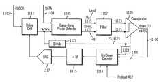
- FIG. 1is a block diagram of an environment in which the invention may be practiced.
- FIG. 2is a schematic of a Hogge-type phase detector.
- FIG. 3is a schematic and block diagram of a Hogge-type phase detector in which appropriate delays have been added to facilitate high-speed operation of the circuit.
- FIG. 4Ais a graphical illustration of phase detector performance for the repetitive data pattern 1100.
- FIG. 4Bis a graphical illustration of phase detector performance for the 1010 repetitive data pattern.
- FIG. 5Ais a graph of ideal phase detector voltage output versus phase for data patterns 1100 and 1010.
- FIG. 5Bis a graph of ideal phase detector output voltage versus phase upon which an actual phase detector output voltage versus phase trace has been superimposed for comparison.
- FIG. 5Cis a graph illustrating two actual phase detector characteristics for different data patterns.
- FIG. 6is an “eye” diagram as may be produced on an oscilloscope by synchronizing a data trace to the data rate.
- FIG. 7Ais a combination block and circuit diagram of a modified Hogge phase detector in which an Alexander type phase detector is used to control the third delay of the modified Hogge phase detector.
- FIG. 7Bis a combination block and circuit diagram of a modified Hogge phase detector circuit in which an Alexander type phase detector is used to control the first delay of the modified Hogge phase detector.
- FIG. 7Cis a combination block and circuit diagram of a modified Hogge phase detector circuit in which an Alexander type phase detector is used to control the second delay of the modified Hogge phase detector.
- FIG. 8Ais a circuit diagram of an exemplary Alexander phase detector as may be used with the delay controlling circuits illustrated in FIG. 7A, 7 B or 7 C.
- FIG. 8Bis an “eye” diagram illustrating the sample times commonly used in phase a detection using a “bang-bang” phase detector.
- FIG. 9is a graph of the phase versus voltage characteristic of a bang bang phase detector.
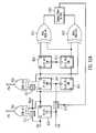
- FIG. 10Ais a combination block and circuit diagram of a modified Hogge phase detector into which an Alexander type phase detector has been integrated.
- FIG. 10Bis a further embodiment of a combination circuit and block diagram of a modified Hogge phase detector into which an Alexander type phase detector has been integrated.
- FIG. 11is a block diagram of a closed loop control system as may be used to control variable circuit delays according to embodiments of the invention.
- FIG. 12is a graphical illustration of a circuit used to differentially integrate the up and down pulse outputs of a “bang-bang” phase detector.
- FIG. 13is a graphical illustration relating the analog input waveform to digital output in a one bit analog to digital converter.
- FIG. 14is a chart relating decimation ratio and clock rate to bandwidth equivalent for variable delay control loops according to embodiments of the invention.
- embodiments of the present inventionrelate, generally, to phase detectors.
- preferred embodimentsare described herein with relation to Sonnet clock data recovery circuits, which employ phase detectors.
- This exemplary embodimentis chosen as an example likely to be familiar to those skilled in the art, but is not intended to limit the invention to the example embodiment.
- the examples disclosedare intended to illustrate the inventive aspects of the present invention, which are applicable to a variety of electronic systems.
- FIG. 1is a block diagram of an environment illustrating according to an example embodiment of the present invention.
- FIG. 1illustrates a block diagram a SONET system.
- SONETis an acronym derived from synchronous optical network.
- SONETis a standard for optical telecommunications data transport formulated by the Exchange Character Standards Association (ECSA) for the American National Standards Institute (ANSI).
- ECSAExchange Character Standards Association
- ANSIis a standards group, which sets industry standards in the United Standards for the telecommunications industry.
- a portion of the SONET networkis illustrated in FIG. 1 .
- the transmitter section of the SONET networkcommonly comprises a laser driver unit 101 into which NRZ data is input 103 .
- the laser driveraccepts the NRZ data and produces laser light pulses, which are then applied to a transport media, typically a fiber optic cable 105 .
- the laser signalis then received in a detector 107 where it is converted back into an electrical signal representing NRZ data.
- the NRZ data signal from the detectoris then coupled into a clock recovery circuit 109 .
- a clock recovery circuitis commonly employed because a clock signal is encoded along with the NRZ data and not transmitted separately.
- the clockis then coupled into a data regenerator 111 that accepts the NRZ signal from the detector 107 as well as the regenerated clock signal, and reproduces the data.
- the regenerated clock signalis recovered from the clock recovery circuit 109 .
- the clock recovery circuit 109synchronizes the regenerated clock with the NRZ signal from detector 107 .
- a phase detector (PD)is the heart of the clock recovery circuit 109 .
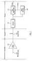
- FIG. 2is an illustration of a Hogge type phase detector.
- a complete description of a Hogge type phase detectormay be found in the paper entitled “A Self-Correcting Clock Recovery Circuit” by Charles R. Hogge Jr., Member IEEE, which may be found in the IEEE Journal of Light Wave Technology, Volume LT-3, pages 312-314, December 1985, which is incorporated by reference herein.
- NRZ datais coupled to data input conductor 201 .
- a recovered clock signalis coupled to clock conductor 223 .
- the first D-type Flip-Flop 203is clocked on the rising edge of the clock signal provided on conductor 223 and the second D Flip-Flop 207 is clocked on the falling edge of the clock signal provided on conductor 223 .
- the datadoes not immediately appear at the Q output of the first Flip-Flop 203 , that is Flip-Flop 203 is not transparent.
- the data presented to Flip-Flop 203 on conductor 201appears at the Q output, and is thereby coupled into conductor 211 upon the occurrence of a rising edge of a clock signal on 223 plus the delays associated with the set up and hold times of the first Flip-Flop 203 . Therefore data, the, that appears on conductor 211 the Q output of D Flip-Flop 203 is re-timed data. After a change in the state of the data input 201 , the D input and Q output of D Flip-Flop 203 are no longer equal, which will cause the output of Exclusive OR gate 205 to go high.
- Exclusive OR 205will remain high until the next rising edge of the clock 223 , when the data input's new state is clocked through Flip-Flop 203 .
- the disparity between the data input 201 and the Q output 211 of Flip-Flop 203is eliminated.
- Exclusive OR gate 209raises its output high because the D and Q lines of Flip-Flop 207 , which are the inputs to the send Exclusive or 209 , are now unequal.
- the output of Exclusive OR 209remains high until the next falling edge of the clock at which time the input data's 201 new state is clocked through Flip-Flop 207 .
- a clock signaltypically has a 50% duty cycle. Assuming a 50% duty cycle, the output 213 of Exclusive OR 209 is a positive pulse with a width equal to half the clock period for each data transition. Exclusive OR 205 's output is also a positive pulse for each data transmission, but its width depends on the phase error between the input data 201 and the clock. The output pulse width of Exclusive OR 205 equals half a clock period when the delay and the clock are optimally aligned. Accordingly, the phase error between the clock and the data can be obtained by comparing the widths of the output pulses of Exclusive ORs 205 and 209 . The output 213 of the first Exclusive OR 205 is coupled into a summation unit 219 .
- the output 215 of the second Exclusive OR 209is also coupled into summation 219 where it is subtracted from the output signal 213 of Exclusive OR 205 .
- the result of the summation in unit 219is a phase detector output 221 . If the phase of the data leads the clock, the output of the phase detector 221 has a positive average value. Conversely, if the phase of the data lags the clock, the phase detector output 221 would have a negative average value. The average output of the phase detector 221 is equal to 0 when the average phase error between the input data and the clock is 0.
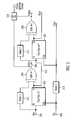
- FIG. 3is a Hogge phase detector circuit in which appropriate delays have been added to facilitate high speed operation of the circuit. As data and clock speeds increase, circuit delays become more significant.
- the first Hogge Flip-Flop 303is clocked on the rising edge of the clock signal 300 . Any data coupled into Flip-Flop 303 on input conductor 301 will appear a time T 1 after the rising edge of the clock.
- T 1Delay 1
- T 1Delay 1
- the output of Exclusive OR 305is the difference between the data input (through Delay One, 311 ) and the previous data which was clocked into Exclusive OR 305 through the first Flip-Flop 303 .
- the output of Exclusive OR 305is a square wave of variable width.
- the width of the square wave output from Exclusive OR 305depends on the relationship between the clock input on conductor 300 and the data input on conductor 301 .
- the first Flip-Flop 303will be clocked to accept data when the data is at midpoint, that is, when the data is halfway between points at which the data may change. Such a point is commonly known in the art as the center of the “eye pattern” or “eye diagram.”
- the “eye pattern” or “eye diagram”refers to the image as seen on an oscilloscope in response to the digital data when the horizontal sweep rate is equal to the baud, bit, or clock rate.
- Such an oscilloscope displayis widely known as an “eye pattern” due to its resemblance to the human eye. Further description of the “eye pattern” may be had by reference to U.S. Pat. No. 3,721,959, which is incorporated by reference herein.
- the output 306 of Exclusive OR 305is dependant upon the data input bit pattern. For example, if the data input is 1010, the output will be a square wave of frequency that is twice the clock rate. However, if the data input is 11001100, the output 306 of Exclusive OR 305 will be a square wave equal in frequency to the clock input. If the data input is 1111000011110000 the output 306 of Exclusive OR 305 will be one-half the input clock rate.
- the error signal 306 of the Hogge phase detectorsin general exhibits a data dependant gain characteristic. The error signal 306 is a combination of error signal combined with phase information.
- the data output of Flip-Flop 303is coupled into conductor 315 .
- the data coupled to conductor 315is synchronous data because it has been synchronized to clock input 300 by Flip-Flop 303 . Therefore the output 310 of the second Exclusive OR 309 is dependant only on the data pattern. Accordingly, when the output 310 of Exclusive OR 309 is subtracted from the output 306 of Exclusive OR 305 , the data dependency disappears and only phase information remains.
- FIG. 4Ais a graphical illustration of phase dependency dependent on data input pattern.
- FIG. 4Ais a graph of a phase detector receiving a 1100 repetitive data pattern in which the phase of the data is swept across a range with respect to the clock.
- Trace 403represents the integration of an error signal, for example, an error signal as illustrated in FIG. 3 at 309 , the output of Exclusive OR 305 .
- Trace 401is an integration of a reference signal; for example the reference signal as depicted in FIG. 3 the output 310 of Exclusive OR 309 .
- the resulting summation of the reference trace 401 and the error trace 403is the phase versus a voltage characteristic of the phase detector.
- error signal 409is plotted against reference signal 407 of the same phase detector as in FIG. 4A except that it is receiving a 1010 data pattern and the phase of the data is being swept across a range with respect to the clock.
- the voltage versus phase curve of FIG. 4B 411is approximately twice the slope of the voltage versus phase curve, 405 , in FIG. 4 A. Accordingly, the phase detector gain of a Hogge-type phase detector receiving a 1100 repeating pattern will be one-half of the gain of the same Hogge phase detector receiving a 1010 repeating pattern.
- FIG. 5Ais an illustrative ideal plot of voltage versus phase for a phase detector circuit such as that illustrated in FIG. 3 .
- Trace 501represents the data pattern 1010 and trace 503 represents the pattern 1100.
- the slope 501 of the phase detector receiving the repetitive 1010 patternis twice the slope 503 of the phase detector receiving the 1100. Additionally, both curves go through the origin of the voltage phase detector graph indicating that at zero volts there is zero phase error, i.e., there is no offset.
- FIG. 5Bis a graph of an ideal phase detector with graph of a typical phase detector superimposed on the same graph.
- voltageis plotted on the vertical axis 513 and phase on the horizontal axis 519 .
- the straight line 507represents an ideal response to a data pattern of 1010.
- the ideal responseis when the voltage versus phase graphs is a straight line as illustrated by trace 507 .
- the characteristic of the phase detector outputtends to decrease towards the end points of the graph as shown by superimposed trace 509 . This reduction in gain is due in part due to bandwidth considerations.
- the problemtends to be exacerbated as the data frequency increases and the roll off, as illustrated by 509 , becomes more pronounced.
- FIG. 5Cis a graph illustrating a phase detector characteristic for two different data patterns.
- data pattern 509has a higher data transition rate than data pattern 511 .
- the data pattern 511also does not cross the voltage versus phase graph at the origin. The result is that a phase offset 513 is produced.
- Curve 509also does not cross the origin and produces offset 515 . Accordingly, the phase detector illustrated in FIG. 5C must traverse a phase, represented by the phase offset between offset 513 and offset 515 when the data pattern switches between the pattern, which produced curve 511 and the pattern, which produced curve 509 .
- phase offsetsmay be due to degradation of data coupled into a phase detector circuit. For example, if the data coupled into a phase detector circuit, e.g. 301 , drops in amplitude, the phase delay through the initial Flip-Flop 303 may change. If the data amplitude is low, the input signal may take longer to cause the Flip-Flop to change states, than if it were the maximum amplitude because the regenerative switching circuitry in the Flip Flop will not be driven as hard by a lower amplitude signal, and hence the signal will take longer to regenerate.
- FIG. 6is an “eye” diagram produced by synchronizing a data to the data rate trace on an oscilloscope.
- the ideal “eye” diagramis shown by trace 601 and trace 603 .
- the eye diagrammay exhibit jitter such as shown by traces 605 and 607 or 609 and 611 when the data pattern changes. This type of phase jitter is more significant as bit rates increase. By diminishing the effects of phase detector rolloff and phase detector offset the maximum frequency data which can be detected in a Hogge type phase detector can be increased.
- circuit delayscan be added to the phase detector circuitry to match clock signal propagation times to those in the data path. Such delays are illustrated in FIG. 3 as delay one ( 311 ), delay three ( 313 ) and delay two ( 317 ).
- Delay 311is used to match signal delay through Flip-Flop 303 . By matching the delay in Flip-Flop 303 to the delay 311 , data can be presented to both inputs of the Exclusive OR gate 305 at the same time thereby eliminating phase errors and race conditions which may adversely affect the performance of the phase detector. In other words the first delay 311 can be used to compensate for the data propagation delay through the first Hogge Flip-Flop 303 .
- the second delay, delay 317can be used to compensate for signal propagation delay through the second Hogge Flip-Flop, Flip-Flop 307 .
- One of the difficulties in matching the first signal delay 311 to the propagation delay of the first Hogge Flip-Flop 303 (as well as matching the second delay 317 to the signal propagation delay of the second Hogge Flip-Flop 307 )is that the input sensitivity of the Flip-Flops may drop as the frequency increases. Additionally propagation delays may vary with temperature in both the delay circuits and the Flip-Flop circuits.
- Delay 313is added to center the clock to-the input data.
- Delay no. 3affects the offset of the phase detector curve and may be used to assure that the phase detector voltage versus frequency curve traverses the origin of the phase detector transfer curve (see FIGS. 5A, 5 B, 5 c ), thereby eliminating any static phase offset.
- Delay 3may be used to set the curve's zero crossing point correctly.
- the matching delayswill need to be adjusted as the propagation delays within the Flip-Flops change.
- the inserted circuit delaysmust be adjusted to compensate for dynamic changes within the phase detector circuitry.
- FIG. 7Ais a combination block and schematic diagram of circuitry used to adjust delay no. 3 of a modified Hogge phase detector.
- the output 705 of the phase detector circuit 701is then coupled into a filter 703 and then further used to control the third delay 313 .
- FIG. 7Bis a combination circuit and block diagram illustrating the use of an Alexander type phase detector to control delay no. 1 of a modified Hogge phase detector circuit.
- the output of first delay 311 of the modified Hogge phase detector circuitis compared with the output of the first Flip-Flop 303 , of the modified Hogge phase detector circuit, in an Alexander (or bang-bang) phase detector 707 .
- the output 709 of the phase detector circuit 707is coupled into a filter and then further used to control the first delay 311 of the modified Hogge phase detector circuit.
- FIG. 7Cis a combination block and circuit diagram of a modified Hogge phase detector circuit in which an Alexander (or bang-bang) type phase detector is used to control the second delay 317 of the modified Hogge phase detector circuit.
- the output of the second delay 317 , of the modified Hogge phase detector circuitis compared to the output of the second Flip-Flop 307 , of the modified Hogge phase detector circuit using an Alexander type phase detector 713 .
- the output 715 of the phase detector 713is then coupled into a filter and the filtered output is then used to control the second delay 317 , of the modified Hogge phase detector circuit.
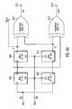
- FIG. 8is a circuit diagram of an Alexander (or bang-bang) phase detector as may be used in FIG. 7A, 7 B or 7 C.
- the phase detectoris one type of phase detector that may be used in the modified Hogge phase detector circuits of 7 A, 7 B and 7 C.
- the Alexander (or bang-bang) phase detectoris a type of phase detector which does not indicate actual phase, but indicates if one signal is leading, lagging, or in phase with a clocking signal.
- the Alexander phase detectoris named for its inventor, J. D. H. Alexander.
- the Alexander phase detectoris described in Electronic Letters by J. D. H. Alexander in an article entitled, Clock Recovery From Random Binary Signals, Volume 11, page 541-542, October 1975, and is incorporated herein by reference.
- the I-diagramis an oscilloscope response to the digital data when the horizontal sweep rate of the oscilloscope is equals the baud rate, byte rate or clock rate.
- the data waveformis sampled at 3 points: A, B and C.
- the sampling at A, B and Ccorresponds to transition times of the clock.
- FIG. 9is a graphical illustration of the curve of a bang-bang phase detector.
- a bang-bang phase detector's two outputsi.e., 817 and 819 ) are commonly translated into three ⁇ output states as seen in FIG. 9 .
- the outputis positive 901 when the signal coupled to the clock input is late with respect to the signal coupled into the data input.
- the bang-bang outputis negative 905 when the clock's signal is early when compared with the data signal input, and the bang-bang output is zero 903 when no decision can be made as to whether the clock and the data are late or early with respect to each other.
- Other variationsare possible, including detectors which merely detect if the last comparison indicated a lagging or leading phase relationship, and the indication does not change when the last indication when the phases are equal.
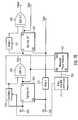
- FIG. 10Ais a combination circuit and block diagram of a modified Hogge phase detector into which an Alexander type phase detector has been integrated.
- the second Flip-Flop 307 of the modified Hogge phase detector circuitis shared with an Alexander type phase detector. This circuit arrangement is convenient because the second Flip-Flop 307 of the modified Hogge phase detector is the same as the first Flip-Flop of the integrated Alexander phase detector.
- the second Flip-Flop 307 of the modified Hogge phase detectoris the circuit which controls the zero crossing point of the Hogge phase detector.
- the first Flip-Flop of the Alexander phase detectoris the Flip-Flop used to control the zero point of the Alexander phase detector. Therefore, the same Flip-Flop controls the zero phase point of both phase detectors.
- FIG. 10Bis a combination circuit and block diagram of a modified Hogge phase detector into which a Alexander phase detector has been integrated.
- FIG. 10Bis similar to FIG. 10 except that in FIG. 10 delay 3 is a single delay while in FIG. 10B delay 3 has been split into complementary delays 313 A and 313 B.
- Delay 313 Aworks in a complementary fashion to delay 3 , that is, as the common control signal (to delays 3 A and 3 B) tends to increase the delay 3 B; it tends to retard delay 3 A.
- FIG. 11is a block diagram of circuitry, which uses a bang-bang phase detector to control local clock delay and thereby synchronize clock signals with data signals.
- Circuitrysuch as illustrated in FIG. 11 can be used with a variety of phase detectors to match clock and data in a variety of points within phase detector circuitry, and is not limited to the illustrative examples which follow.
- a clock signal 1101is coupled into a delay cell 1113 .
- the present exemplary implementationprovides a delay cell, such as 1113 , in line with the clock signal delays can alternately be inserted into a data line and complimentary delays can be inserted into both data and clock lines.
- Complimentary delays and data and clock linescan produce an increasing delay in one line and a decreasing delay in the second line in order to match the phase of the clock and data signals.
- the delayed clock signalemerges from the delay cell 113 and then is coupled into a bang-bang phase detector 1105 .
- the bang-bang phase detector 1105compares the delayed clock with data input 1103 and produces output pulses.
- the bang-bang phase detectorproduces up pulses if the clock leads the data and produces down pulses if the clock lags the data.
- Bang-bang phase detectorsi.e., Alexander type phase detectors, generally can tell if the clock leads the data, follows the data and some can determine if the clock phase is equal to the phase of the data.
- a bang-bang phase detectorno information on how much a clock signal leads or lags a data signal is developed by a bang-bang phase detector.
- the up signal 1119 and the down signal 1121 from the bang-bang phase detectoris coupled into a filter 1107 .
- the filteris further illustrated in FIG. 12 .
- FIG. 12is a graphical illustration of a filter as may be used to integrate the output of a bang-bang phase detector.
- the exemplary filter in FIG. 12comprises a capacitor 1205 .
- the positive side of capacitor 1205accepts up pulses on line 1119 from the bang-bang phase detector.
- the capacitor 1205also accepts down pulses from output 1121 , the down output of the bang-bang phase detector 1105 .
- the up pulses, represented by 1201 and the down pulses represented by 1203are coupled across the capacitor 1205 to form a differential voltage (Vdif) 1207 measured across outputs 1123 and 1125 of the filter 1107 .
- Graph 1301is an illustration of Vdif 1207 as it switches between-positive and negative values.
- the outputs 1123 and 1125 from the filter 1107are coupled into a comparator 1107 .
- the output of the comparator 1109is a 1 if the Vdif voltage is positive and is zero if the Vdif voltage is negative.
- the relationship between Vdif voltage and the output of comparator 1109are illustrated in FIG. 13 .
- FIG. 13is a graphical comparison of Vdif voltage into comparator 1109 as compared with the output 1110 of comparator 1109 .
- Vdifis a positive value
- the output 1110 of comparator 1109is has a value of “1” as shown in trace 1303 .
- Vdifis less than zero
- the output of 1110 of comparator 1109is a “0” value, also as shown in trace 1303 .
- the Vdif signalis sampled by the comparator 1109 at times dictated by a clock signal, which is the result of dividing the delayed clock signal by divider 1127 .
- the divided clock output from divider 1127is also coupled into a further divider 1129 and used to clock an up/down counter 1111 .
- the up/down counter 1111receives the output from the comparator 1109 . If the output of the comparator 1109 is a “1”, then the up/down counter 1111 will count down. If the output of comparator 1109 is a “0”, then the up/down counter 1111 will count up.
- the up/down counteralso may be preloaded with an initial starting value using preload input 1114 .
- the output of the up/down counteris then further coupled into a divide by M circuit 1115 , which decimates (reduces by a factor) the input count.
- the divide by M circuitmay sample the most significant byte of up/down counter 1111 ; it may also sample all of the K-bytes of up/down counter 1111 or any range in between.
- the output of up/down counter 1111is then further decimated in a divide circuit 1115 , where the output of the up/down counter 1111 is divided by M.
- the output of divider 1115is then further coupled into a digital-to-analog converter 1117 which is then further coupled into delay cell 1113 in order to troll the amount of delay caused by delay cell 1113 .
- Delay cell 1113may also be controlled directly from the digital. output of the divide by M circuit 1115 . If the delay cell 1113 is directly controlled by the digital output of the divide by M circuit, then the digital-to-analog converter 1117 may be eliminated.
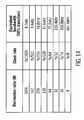
- FIG. 14is an example of how controlling the decimation ratio of divide by circuit 1115 and of controlling the divide circuit 1129 can control the frequency response of the delay cell control loop.
- the decimation ratiois 1024 , meaning that divide by counter 1115 divides its input by 1024 , and if the up/down counter is clocked at a clock rate which is equal to the sample rate FS, 1129, divided by 1024, then the equivalent bandwidth of the delay cell control loop is 4.7 KHz.
- the equivalent bandwidthbecomes 601.6 KHz as shown in FIG. 14 .
- the decimation ratiois increased from 1024, (i.e. 1K) to 8182, (i.e. 8K) while holding the clock rate to fs/1024.
- An equivalent bandwidth of approximately 500 Hzresults. Because the change in circuit delays primarily results from slow changing factors, such as circuit temperature, a 500 Hz delay cell control loop bandwidth can be more than adequate to sufficiently control the offsets that delay cell 1113 will need to compensate.
- a configuration such as that illustrated in FIG. 11can provide a range of benefits to electronic systems.
- the filter 1107provides a first benefit. By coupling the up pulses of a bang-bang phase detector into one-side of a capacitor (e.g. 1205 ) and coupling the down pulses of a bang-bang phase detector into the other side of a capacitor a differential integrator results. Because the filter 1107 is a differential integrator, it will exhibit a voltage that is related to the differential in the number of pulses produced by the up 1119 and the down 1121 outputs of the bang-bang phase detector 1105 . The output of the filter 1107 is then a signal which represents an average indicating whether the clock is leading the data or vice versa.
- the up/down counter 1111provides a second advantage.
- the up/down counter 1111can provide a convenient way to increase and decrease the bandwidth of the delay control loop.
- the bandwidth of the delay control loopcan be increased by increasing the clock frequency of the up/down counter 1111 and be decreased by decreasing the clock frequency of the up/down counter 1111 .
- the clock of the up/down counter 1111can be increased or decreased easily by changing a divide by ratio 1129 in line with the up/down counter clock, the bandwidth of the system can be controlled dynamically. For example, when the loop is initially started, the response of the loop can be increased in order to facilitate signal acquisition and lock. Conversely, the loop can be desensitized by decreasing the frequency of the up/down counter clock, thereby lowering the bandwidth of the loop.
- a further advantage of the circuitry as depicted in FIG. 11is that the up/down counter 1111 can be preloaded with a value. This value can represent the steady state value that the loop settled into the last time it was active thereby reducing the time necessary for the delay cell control loop of FIG. 11 to settle to the correct delay value.
- the up/down countercan also be preloaded with a number representing the offset as the pattern of the data received changes. For example, with respect to FIG. 5C, if curve 509 represents header data and curve 511 represents normal data, then during the period where the header is being received, the offset will be as shown in FIG. 5C at 515 . Once the end of the header is detected, the offset will be 515 as represented by curve 511 . When the end of the header data is detected, the counter can be preloaded with a number representing the offset 513 thereby facilitating settling of the loop to the correct offset.
Landscapes
- Engineering & Computer Science (AREA)
- Computer Networks & Wireless Communication (AREA)
- Signal Processing (AREA)
- Stabilization Of Oscillater, Synchronisation, Frequency Synthesizers (AREA)
Abstract
Description
Claims (2)
Priority Applications (1)
| Application Number | Priority Date | Filing Date | Title |
|---|---|---|---|
| US09/615,627US6526109B1 (en) | 1999-07-16 | 2000-12-05 | Method and apparatus for hybrid smart center loop for clock data recovery |
Applications Claiming Priority (2)
| Application Number | Priority Date | Filing Date | Title |
|---|---|---|---|
| US14443299P | 1999-07-16 | 1999-07-16 | |
| US09/615,627US6526109B1 (en) | 1999-07-16 | 2000-12-05 | Method and apparatus for hybrid smart center loop for clock data recovery |
Publications (1)
| Publication Number | Publication Date |
|---|---|
| US6526109B1true US6526109B1 (en) | 2003-02-25 |
Family
ID=22508578
Family Applications (2)
| Application Number | Title | Priority Date | Filing Date |
|---|---|---|---|
| US09/615,631Expired - LifetimeUS6316966B1 (en) | 1999-07-16 | 2000-07-13 | Apparatus and method for servo-controlled self-centering phase detector |
| US09/615,627Expired - LifetimeUS6526109B1 (en) | 1999-07-16 | 2000-12-05 | Method and apparatus for hybrid smart center loop for clock data recovery |
Family Applications Before (1)
| Application Number | Title | Priority Date | Filing Date |
|---|---|---|---|
| US09/615,631Expired - LifetimeUS6316966B1 (en) | 1999-07-16 | 2000-07-13 | Apparatus and method for servo-controlled self-centering phase detector |
Country Status (2)
| Country | Link |
|---|---|
| US (2) | US6316966B1 (en) |
| WO (1) | WO2001006696A1 (en) |
Cited By (34)
| Publication number | Priority date | Publication date | Assignee | Title |
|---|---|---|---|---|
| US20020070752A1 (en)* | 2000-08-30 | 2002-06-13 | Harrison Ronnie M. | Method and system for controlling the duty cycle of a clock signal |
| US20030091139A1 (en)* | 2001-09-18 | 2003-05-15 | Jun Cao | System and method for adjusting phase offsets |
| US20030221143A1 (en)* | 2002-05-23 | 2003-11-27 | Kurd Nasser A. | Circuit to manage and lower clock inaccuracies of integrated circuits |
| US20040061539A1 (en)* | 2002-09-27 | 2004-04-01 | Geertjan Joordens | Linear half-rate phase detector for clock recovery and method therefor |
| US20040091064A1 (en)* | 2002-11-12 | 2004-05-13 | Broadcom Corporation | Phase detector with delay elements for improved data regeneration |
| US20040247066A1 (en)* | 2001-10-19 | 2004-12-09 | Masakatsu Suda | Phase-locked loop circuit, delay locked loop circuit, timing generator, semiconductor test instrument, and semiconductor integrated circuit |
| US6836167B2 (en)* | 2002-07-17 | 2004-12-28 | Intel Corporation | Techniques to control signal phase |
| US20050031065A1 (en)* | 2003-08-06 | 2005-02-10 | Gupta Atul K. | System and method for automatically correcting duty cycle distortion |
| US20050134338A1 (en)* | 2003-12-19 | 2005-06-23 | Afshin Momtaz | High frequency binary phase detector |
| US20050238092A1 (en)* | 2004-04-22 | 2005-10-27 | Ng Devin K | Method and system for error estimation for adaptive equalization in communication systems |
| EP1623794A1 (en) | 2004-08-05 | 2006-02-08 | MTU Aero Engines GmbH | Device for peening workpiece surfaces |
| US7050463B1 (en)* | 2000-10-31 | 2006-05-23 | Texas Instruments Incorporated | Automatic bit-rate detection scheme for use on SONET transceiver |
| EP1701444A1 (en)* | 2005-03-08 | 2006-09-13 | Synthesys Research, Inc. | Method and apparatus for detecting linear phase error |
| US20060227914A1 (en)* | 2005-03-30 | 2006-10-12 | Hamid Partovi | Clock data recovery circuit with circuit loop disablement |
| US20070064848A1 (en)* | 2005-09-21 | 2007-03-22 | Jayen Desai | Clock recovery |
| US20070208819A1 (en)* | 2006-03-06 | 2007-09-06 | Advanced Micro Devices, Inc. | Asymmetric control of high-speed bidirectional signaling |
| US20070268962A1 (en)* | 2006-05-16 | 2007-11-22 | Mobin Mohammad S | Methods and apparatus for evaluating the eye margin of a communications device using a data eye monitor |
| US7386084B2 (en)* | 2002-11-06 | 2008-06-10 | Broadcom Corporation | Method and system for pattern-independent phase adjustment in a clock and data recovery (CDR) circuit |
| US20090041173A1 (en)* | 2005-11-14 | 2009-02-12 | Lin Wen T | Data clock recovery system using digital arrival-time detector |
| US7505332B1 (en) | 2006-03-06 | 2009-03-17 | Advanced Micro Devices, Inc. | Input offset correction for asymmetric control of high-speed bidirectional signaling |
| US7506222B1 (en)* | 2006-03-06 | 2009-03-17 | Advanced Micro Devices, Inc. | System for phase tracking and equalization across a byte group for asymmetric control of high-speed bidirectional signaling |
| US20090110136A1 (en)* | 2007-10-31 | 2009-04-30 | Riccardo Badalone | Bang-bang phase detector with sub-rate clock |
| US20090251225A1 (en)* | 2008-04-02 | 2009-10-08 | Shuo-Wei Chen | Fractional And Integer PLL Architectures |
| US20090278576A1 (en)* | 2008-05-07 | 2009-11-12 | Lsi Corporation | Critical path monitor for an integrated circuit and method of operation thereof |
| US20100098150A1 (en)* | 2008-10-16 | 2010-04-22 | Soni Samir J | Techniques for Asynchronous Data Recovery |
| US20100148832A1 (en)* | 2008-12-16 | 2010-06-17 | Nec Electronics Corporation | Clock data recovery circuit |
| US20100166129A1 (en)* | 2008-12-30 | 2010-07-01 | Kyoo-Joon Lee | Data transmitting device and data receiving device |
| US20100246735A1 (en)* | 2009-03-27 | 2010-09-30 | Freescale Semiconductor, Inc. | Asynchronous data recovery methods and apparatus |
| US7929654B2 (en) | 2007-08-30 | 2011-04-19 | Zenko Technologies, Inc. | Data sampling circuit and method for clock and data recovery |
| US20130077724A1 (en)* | 2011-09-23 | 2013-03-28 | International Business Machines Corporation | Digital phase detector with zero phase offset |
| US20150333902A1 (en)* | 2012-01-31 | 2015-11-19 | Texas Instruments Incorporated | Data transfer clock recovery for legacy systems |
| TWI648954B (en)* | 2017-10-31 | 2019-01-21 | 北京集創北方科技股份有限公司 | Clock data recovery circuit with adaptive loop bandwidth adjustment mechanism and communication device using same |
| TWI734655B (en)* | 2020-12-07 | 2021-07-21 | 瑞鼎科技股份有限公司 | A method for improving the tracking performance of clock data recovery circuitand a system using the same |
| US11979163B2 (en)* | 2022-10-03 | 2024-05-07 | Western Digital Technologies, Inc. | Oversampled phase lock loop in a read channel |
Families Citing this family (24)
| Publication number | Priority date | Publication date | Assignee | Title |
|---|---|---|---|---|
| US6847789B2 (en) | 2000-02-17 | 2005-01-25 | Broadcom Corporation | Linear half-rate phase detector and clock and data recovery circuit |
| US6909852B2 (en) | 2000-02-17 | 2005-06-21 | Broadcom Corporation | Linear full-rate phase detector and clock and data recovery circuit |
| WO2001067612A1 (en)* | 2000-03-07 | 2001-09-13 | Koninklijke Philips Electronics N.V. | Data clocked recovery circuit |
| US6807225B1 (en)* | 2000-05-31 | 2004-10-19 | Conexant Systems, Inc. | Circuit and method for self trimming frequency acquisition |
| US20020093986A1 (en)* | 2000-12-30 | 2002-07-18 | Norm Hendrickson | Forward data de-skew method and system |
| US20020093994A1 (en)* | 2000-12-30 | 2002-07-18 | Norm Hendrickson | Reverse data de-skew method and system |
| US20020090045A1 (en)* | 2001-01-10 | 2002-07-11 | Norm Hendrickson | Digital clock recovery system |
| US7123678B2 (en) | 2001-02-01 | 2006-10-17 | Vitesse Semiconductor Corporation | RZ recovery |
| US7116744B2 (en) | 2001-03-29 | 2006-10-03 | Fujitsu Limited | Clock recovery circuit and receiver circuit for improving the error rate of signal reproduction |
| GB0111300D0 (en)* | 2001-05-09 | 2001-06-27 | Mitel Knowledge Corp | Method and apparatus for synchronizing slave network node to master network node |
| US6988227B1 (en) | 2001-06-25 | 2006-01-17 | Silicon Laboratories Inc. | Method and apparatus for bit error rate detection |
| US6856206B1 (en)* | 2001-06-25 | 2005-02-15 | Silicon Laboratories, Inc. | Method and apparatus for acquiring a frequency without a reference clock |
| US7068726B1 (en)* | 2001-08-30 | 2006-06-27 | 3Com Corporation | Near end cross-talk and echo avoider for bi-directional digital communications |
| US20030190001A1 (en)* | 2002-04-08 | 2003-10-09 | Exar Corporation | Clock and data recovery circuit for return-to-zero data |
| US7028205B2 (en)* | 2002-07-25 | 2006-04-11 | Intel Corporation | Techniques to monitor transition density of an input signal |
| US20040153681A1 (en)* | 2002-11-12 | 2004-08-05 | Broadcom Corporation | Phase detector for extended linear response and high-speed data regeneration |
| US7119727B2 (en)* | 2004-10-25 | 2006-10-10 | Atmel Corporation | Analog-to-digital converter |
| JP4437541B2 (en)* | 2004-11-17 | 2010-03-24 | 富士通マイクロエレクトロニクス株式会社 | Reset control circuit and reset control method |
| EP1894296B1 (en)* | 2005-05-24 | 2011-04-13 | Finisar Corporation | Pattern-dependent phase detector for clock recovery |
| JP4679273B2 (en)* | 2005-07-05 | 2011-04-27 | ルネサスエレクトロニクス株式会社 | Clock data recovery circuit |
| TW200727590A (en)* | 2006-01-04 | 2007-07-16 | Via Tech Inc | Test apparatus of clock signal |
| US7375591B2 (en)* | 2006-08-04 | 2008-05-20 | Silicon Laboratories Inc. | Robust false locking prevention in referenceless frequency acquisition |
| US8958513B1 (en)* | 2013-03-15 | 2015-02-17 | Xilinx, Inc. | Clock and data recovery with infinite pull-in range |
| JP6475202B2 (en)* | 2016-07-21 | 2019-02-27 | Necプラットフォームズ株式会社 | Phase comparison circuit and control method thereof |
Citations (12)
| Publication number | Priority date | Publication date | Assignee | Title |
|---|---|---|---|---|
| US4218771A (en) | 1978-12-04 | 1980-08-19 | Rockwell International Corporation | Automatic clock positioning circuit for a digital data transmission system |
| US4422176A (en) | 1980-12-12 | 1983-12-20 | U.S. Philips Corporation | Phase sensitive detector |
| US4724401A (en) | 1987-04-23 | 1988-02-09 | Rockwell International Corporation | Adaptive oscillator apparatus for use in a phase-lock loop |
| US4881243A (en) | 1984-06-07 | 1989-11-14 | British Telecommunications Public Limited Company | Signal timing circuits |
| US5687202A (en)* | 1995-04-24 | 1997-11-11 | Cyrix Corporation | Programmable phase shift clock generator |
| US5799048A (en) | 1996-04-17 | 1998-08-25 | Sun Microsystems, Inc. | Phase detector for clock synchronization and recovery |
| US5877641A (en)* | 1993-12-10 | 1999-03-02 | Texas Instruments Incorporated | Clock generator and phase comparator for use in such a clock generator |
| GB2331416A (en) | 1997-08-27 | 1999-05-19 | Lsi Logic Corp | Continuously adjustable delay circuit |
| US5945862A (en)* | 1997-07-31 | 1999-08-31 | Rambus Incorporated | Circuitry for the delay adjustment of a clock signal |
| US5973524A (en)* | 1998-03-25 | 1999-10-26 | Silsym, Inc. | Obtaining accurate on-chip time-constants and conductances |
| WO2000031914A2 (en) | 1998-11-24 | 2000-06-02 | Giga A/S | A method and a circuit for recovering a digital data signal and a clock from a received data signal |
| US6356122B2 (en)* | 1998-08-05 | 2002-03-12 | Cypress Semiconductor Corp. | Clock synthesizer with programmable input-output phase relationship |
Family Cites Families (4)
| Publication number | Priority date | Publication date | Assignee | Title |
|---|---|---|---|---|
| IT1231650B (en)* | 1989-07-21 | 1991-12-18 | Selenia Ind Elettroniche | CIRCUIT FOR THE RECONSTRUCTION OF THE CLOCK FROM A MESSAGE TO BE USED IN DATA TRANSMISSION SYSTEMS |
| JP2837982B2 (en)* | 1991-12-27 | 1998-12-16 | 三菱電機株式会社 | Delay detection demodulator |
| US5455540A (en)* | 1994-10-26 | 1995-10-03 | Cypress Semiconductor Corp. | Modified bang-bang phase detector with ternary output |
| US6151356A (en)* | 1997-04-28 | 2000-11-21 | Nortel Networks Limited | Method and apparatus for phase detection in digital signals |
- 2000
- 2000-07-13USUS09/615,631patent/US6316966B1/ennot_activeExpired - Lifetime
- 2000-07-13WOPCT/US2000/018993patent/WO2001006696A1/enactiveSearch and Examination
- 2000-12-05USUS09/615,627patent/US6526109B1/ennot_activeExpired - Lifetime
Patent Citations (12)
| Publication number | Priority date | Publication date | Assignee | Title |
|---|---|---|---|---|
| US4218771A (en) | 1978-12-04 | 1980-08-19 | Rockwell International Corporation | Automatic clock positioning circuit for a digital data transmission system |
| US4422176A (en) | 1980-12-12 | 1983-12-20 | U.S. Philips Corporation | Phase sensitive detector |
| US4881243A (en) | 1984-06-07 | 1989-11-14 | British Telecommunications Public Limited Company | Signal timing circuits |
| US4724401A (en) | 1987-04-23 | 1988-02-09 | Rockwell International Corporation | Adaptive oscillator apparatus for use in a phase-lock loop |
| US5877641A (en)* | 1993-12-10 | 1999-03-02 | Texas Instruments Incorporated | Clock generator and phase comparator for use in such a clock generator |
| US5687202A (en)* | 1995-04-24 | 1997-11-11 | Cyrix Corporation | Programmable phase shift clock generator |
| US5799048A (en) | 1996-04-17 | 1998-08-25 | Sun Microsystems, Inc. | Phase detector for clock synchronization and recovery |
| US5945862A (en)* | 1997-07-31 | 1999-08-31 | Rambus Incorporated | Circuitry for the delay adjustment of a clock signal |
| GB2331416A (en) | 1997-08-27 | 1999-05-19 | Lsi Logic Corp | Continuously adjustable delay circuit |
| US5973524A (en)* | 1998-03-25 | 1999-10-26 | Silsym, Inc. | Obtaining accurate on-chip time-constants and conductances |
| US6356122B2 (en)* | 1998-08-05 | 2002-03-12 | Cypress Semiconductor Corp. | Clock synthesizer with programmable input-output phase relationship |
| WO2000031914A2 (en) | 1998-11-24 | 2000-06-02 | Giga A/S | A method and a circuit for recovering a digital data signal and a clock from a received data signal |
Non-Patent Citations (5)
| Title |
|---|
| B. Razavi and J. Sung, "A 6 GHz 60 mW BiCMOS Phase-Locked Loop", pp. 320-325, reprinted from IEEE J. Solid-State Circ., vol. SC-29, pp. 1560-1565, Dec. 1994. |
| B. Razavi, "Monolithic Phase-Locked Loops and Clock Recovery Circuits". Piscataway, NJ: IEEE Press, 1996. |
| J.D.H. Alexander, "Clock Recovery From Random Binary Signals", pp. 242-243, reprinted form Electronics Letters, vol. 11, pp. 541-542, Oct. 1975. |
| PCT International Search Report in PCT/US00/18993 dated Oct. 17, 2000. |
| T. Lee and J. Bulzacchelli, "A 155-MHz Clock Recovery Delay and Phase-Locked Loop", pp. 421-430, reprinted from IEEE J. Solid-State Circuits, vol. 27, pp. 1736-1746, Dec. 1992. |
Cited By (60)
| Publication number | Priority date | Publication date | Assignee | Title |
|---|---|---|---|---|
| US20020070752A1 (en)* | 2000-08-30 | 2002-06-13 | Harrison Ronnie M. | Method and system for controlling the duty cycle of a clock signal |
| US6744281B2 (en) | 2000-08-30 | 2004-06-01 | Micron Technology, Inc. | Method and system for controlling the duty cycle of a clock signal |
| US6781419B2 (en) | 2000-08-30 | 2004-08-24 | Micron Technology, Inc. | Method and system for controlling the duty cycle of a clock signal |
| US7050463B1 (en)* | 2000-10-31 | 2006-05-23 | Texas Instruments Incorporated | Automatic bit-rate detection scheme for use on SONET transceiver |
| US20030091139A1 (en)* | 2001-09-18 | 2003-05-15 | Jun Cao | System and method for adjusting phase offsets |
| US7535273B2 (en)* | 2001-10-19 | 2009-05-19 | Advantest Corp. | Phase-locked loop circuit, delay locked loop circuit, timing generator, semiconductor test instrument, and semiconductor integrated circuit |
| US20080143399A1 (en)* | 2001-10-19 | 2008-06-19 | Advantest Corporation | Phase-locked loop circuit, delay locked loop circuit, timing generator, semiconductor test instrument, and semiconductor integrated circuit |
| US7492198B2 (en)* | 2001-10-19 | 2009-02-17 | Advantest Corp. | Phase-locked loop circuit, delay locked loop circuit, timing generator, semiconductor test instrument, and semiconductor integrated circuit |
| US20040247066A1 (en)* | 2001-10-19 | 2004-12-09 | Masakatsu Suda | Phase-locked loop circuit, delay locked loop circuit, timing generator, semiconductor test instrument, and semiconductor integrated circuit |
| US7102402B2 (en)* | 2002-05-23 | 2006-09-05 | Intel Corporation | Circuit to manage and lower clock inaccuracies of integrated circuits |
| US20030221143A1 (en)* | 2002-05-23 | 2003-11-27 | Kurd Nasser A. | Circuit to manage and lower clock inaccuracies of integrated circuits |
| US6836167B2 (en)* | 2002-07-17 | 2004-12-28 | Intel Corporation | Techniques to control signal phase |
| US20040061539A1 (en)* | 2002-09-27 | 2004-04-01 | Geertjan Joordens | Linear half-rate phase detector for clock recovery and method therefor |
| US7236551B2 (en)* | 2002-09-27 | 2007-06-26 | Nxp B.V. | Linear half-rate phase detector for clock recovery and method therefor |
| US7386084B2 (en)* | 2002-11-06 | 2008-06-10 | Broadcom Corporation | Method and system for pattern-independent phase adjustment in a clock and data recovery (CDR) circuit |
| US20040091064A1 (en)* | 2002-11-12 | 2004-05-13 | Broadcom Corporation | Phase detector with delay elements for improved data regeneration |
| US20050031065A1 (en)* | 2003-08-06 | 2005-02-10 | Gupta Atul K. | System and method for automatically correcting duty cycle distortion |
| US7292670B2 (en) | 2003-08-06 | 2007-11-06 | Gennum Corporation | System and method for automatically correcting duty cycle distortion |
| US20050134338A1 (en)* | 2003-12-19 | 2005-06-23 | Afshin Momtaz | High frequency binary phase detector |
| US7202707B2 (en)* | 2003-12-19 | 2007-04-10 | Broadcom Corporation | High frequency binary phase detector |
| US20050238092A1 (en)* | 2004-04-22 | 2005-10-27 | Ng Devin K | Method and system for error estimation for adaptive equalization in communication systems |
| US20060174483A1 (en)* | 2004-08-05 | 2006-08-10 | Erwin Bayer | Device for surface blasting component |
| EP1623794A1 (en) | 2004-08-05 | 2006-02-08 | MTU Aero Engines GmbH | Device for peening workpiece surfaces |
| EP1701444A1 (en)* | 2005-03-08 | 2006-09-13 | Synthesys Research, Inc. | Method and apparatus for detecting linear phase error |
| US7681063B2 (en) | 2005-03-30 | 2010-03-16 | Infineon Technologies Ag | Clock data recovery circuit with circuit loop disablement |
| US20060227914A1 (en)* | 2005-03-30 | 2006-10-12 | Hamid Partovi | Clock data recovery circuit with circuit loop disablement |
| US7873132B2 (en) | 2005-09-21 | 2011-01-18 | Hewlett-Packard Development Company, L.P. | Clock recovery |
| US20070064848A1 (en)* | 2005-09-21 | 2007-03-22 | Jayen Desai | Clock recovery |
| US20090041173A1 (en)* | 2005-11-14 | 2009-02-12 | Lin Wen T | Data clock recovery system using digital arrival-time detector |
| US7506222B1 (en)* | 2006-03-06 | 2009-03-17 | Advanced Micro Devices, Inc. | System for phase tracking and equalization across a byte group for asymmetric control of high-speed bidirectional signaling |
| US7729465B2 (en) | 2006-03-06 | 2010-06-01 | Globalfoundries Inc. | Asymmetric control of high-speed bidirectional signaling |
| US7505332B1 (en) | 2006-03-06 | 2009-03-17 | Advanced Micro Devices, Inc. | Input offset correction for asymmetric control of high-speed bidirectional signaling |
| US20070208819A1 (en)* | 2006-03-06 | 2007-09-06 | Advanced Micro Devices, Inc. | Asymmetric control of high-speed bidirectional signaling |
| US8126039B2 (en)* | 2006-05-16 | 2012-02-28 | Agere Systems Inc. | Methods and apparatus for evaluating the eye margin of a communications device using a data eye monitor |
| US20070268962A1 (en)* | 2006-05-16 | 2007-11-22 | Mobin Mohammad S | Methods and apparatus for evaluating the eye margin of a communications device using a data eye monitor |
| US7929654B2 (en) | 2007-08-30 | 2011-04-19 | Zenko Technologies, Inc. | Data sampling circuit and method for clock and data recovery |
| US8315349B2 (en) | 2007-10-31 | 2012-11-20 | Diablo Technologies Inc. | Bang-bang phase detector with sub-rate clock |
| US20090110136A1 (en)* | 2007-10-31 | 2009-04-30 | Riccardo Badalone | Bang-bang phase detector with sub-rate clock |
| US8890624B2 (en) | 2008-04-02 | 2014-11-18 | Qualcomm Incorporated | Fractional and integer PLL architectures |
| WO2009124145A3 (en)* | 2008-04-02 | 2010-01-07 | Atheros Communications, Inc. | Fractional and integer pll architectures |
| US20090251225A1 (en)* | 2008-04-02 | 2009-10-08 | Shuo-Wei Chen | Fractional And Integer PLL Architectures |
| US8289086B2 (en) | 2008-04-02 | 2012-10-16 | Qualcomm Atheros, Inc. | Fractional and integer PLL architectures |
| US20090278576A1 (en)* | 2008-05-07 | 2009-11-12 | Lsi Corporation | Critical path monitor for an integrated circuit and method of operation thereof |
| US8499230B2 (en)* | 2008-05-07 | 2013-07-30 | Lsi Corporation | Critical path monitor for an integrated circuit and method of operation thereof |
| US8265216B2 (en) | 2008-10-16 | 2012-09-11 | Freescale Semiconductor, Inc. | Techniques for asynchronous data recovery |
| US20100098150A1 (en)* | 2008-10-16 | 2010-04-22 | Soni Samir J | Techniques for Asynchronous Data Recovery |
| US20100148832A1 (en)* | 2008-12-16 | 2010-06-17 | Nec Electronics Corporation | Clock data recovery circuit |
| US8170168B2 (en)* | 2008-12-16 | 2012-05-01 | Renesas Electronics Corporation | Clock data recovery circuit |
| US7876130B2 (en)* | 2008-12-30 | 2011-01-25 | Dongbu Hitek Co., Ltd. | Data transmitting device and data receiving device |
| US20100166129A1 (en)* | 2008-12-30 | 2010-07-01 | Kyoo-Joon Lee | Data transmitting device and data receiving device |
| US20100246735A1 (en)* | 2009-03-27 | 2010-09-30 | Freescale Semiconductor, Inc. | Asynchronous data recovery methods and apparatus |
| US8630382B2 (en) | 2009-03-27 | 2014-01-14 | Freescale Semiconductor, Inc. | Asynchronous data recovery methods and apparatus |
| US8718216B2 (en)* | 2011-09-23 | 2014-05-06 | International Business Machines Corporation | Digital phase detector with zero phase offset |
| US8824573B2 (en) | 2011-09-23 | 2014-09-02 | International Business Machines Corporation | Digital phase detector with zero phase offset |
| US20130077724A1 (en)* | 2011-09-23 | 2013-03-28 | International Business Machines Corporation | Digital phase detector with zero phase offset |
| US20150333902A1 (en)* | 2012-01-31 | 2015-11-19 | Texas Instruments Incorporated | Data transfer clock recovery for legacy systems |
| US9419788B2 (en)* | 2012-01-31 | 2016-08-16 | Texas Instruments Incorporated | Data transfer clock recovery for legacy systems |
| TWI648954B (en)* | 2017-10-31 | 2019-01-21 | 北京集創北方科技股份有限公司 | Clock data recovery circuit with adaptive loop bandwidth adjustment mechanism and communication device using same |
| TWI734655B (en)* | 2020-12-07 | 2021-07-21 | 瑞鼎科技股份有限公司 | A method for improving the tracking performance of clock data recovery circuitand a system using the same |
| US11979163B2 (en)* | 2022-10-03 | 2024-05-07 | Western Digital Technologies, Inc. | Oversampled phase lock loop in a read channel |
Also Published As
| Publication number | Publication date |
|---|---|
| WO2001006696A1 (en) | 2001-01-25 |
| US6316966B1 (en) | 2001-11-13 |
Similar Documents
| Publication | Publication Date | Title |
|---|---|---|
| US6526109B1 (en) | Method and apparatus for hybrid smart center loop for clock data recovery | |
| AU2001286987B2 (en) | Digital-data receiver synchronization method and apparatus | |
| US5987085A (en) | Clock recovery circuit | |
| US5012494A (en) | Method and apparatus for clock recovery and data retiming for random NRZ data | |
| KR970003097B1 (en) | Pll | |
| KR100234551B1 (en) | Phase Detectors for Microwave Clock and Data Recovery Circuits | |
| US5592125A (en) | Modified bang-bang phase detector with ternary output | |
| AU2001286987A1 (en) | Digital-data receiver synchronization method and apparatus | |
| US5276712A (en) | Method and apparatus for clock recovery in digital communication systems | |
| US7324620B2 (en) | Techniques to reduce transmitted jitter | |
| EP0168943B1 (en) | Signal timing circuits | |
| EP1183781A1 (en) | Data clock recovery circuit | |
| JP3351407B2 (en) | CDR circuit for optical receiver | |
| US6389090B2 (en) | Digital clock/data signal recovery method and apparatus | |
| EP1006660B1 (en) | Clock reproduction and identification apparatus | |
| US20050163272A1 (en) | High speed early/late discrimination systems and methods for clock and data recovery receivers | |
| US6549598B1 (en) | Clock signal extraction circuit | |
| CN100555931C (en) | The device of conditioning signal sampled point, system and method | |
| US5612938A (en) | Correcting recorded marks and land lengths taken from an optical disk | |
| KR100261287B1 (en) | Phase Comparison Detector and Detection Method by Signal Transition Method | |
| JPS64859B2 (en) | ||
| JPS60198945A (en) | code identifier |
Legal Events
| Date | Code | Title | Description |
|---|---|---|---|
| AS | Assignment | Owner name:CONEXANT SYSTEMS, INC., CALIFORNIA Free format text:ASSIGNMENT OF ASSIGNORS INTEREST;ASSIGNORS:CHANG, CHARLES;ZHANG, BO;LAO, ZHIHAO;REEL/FRAME:011365/0891;SIGNING DATES FROM 20001024 TO 20001211 | |
| STCF | Information on status: patent grant | Free format text:PATENTED CASE | |
| FPAY | Fee payment | Year of fee payment:4 | |
| AS | Assignment | Owner name:BANK OF NEW YORK TRUST COMPANY, N.A.,ILLINOIS Free format text:SECURITY AGREEMENT;ASSIGNOR:CONEXANT SYSTEMS, INC.;REEL/FRAME:018711/0818 Effective date:20061113 Owner name:BANK OF NEW YORK TRUST COMPANY, N.A., ILLINOIS Free format text:SECURITY AGREEMENT;ASSIGNOR:CONEXANT SYSTEMS, INC.;REEL/FRAME:018711/0818 Effective date:20061113 | |
| AS | Assignment | Owner name:CONEXANT SYSTEMS, INC.,CALIFORNIA Free format text:RELEASE BY SECURED PARTY;ASSIGNOR:THE BANK OF NEW YORK MELLON TRUST COMPANY, N.A. (FORMERLY, THE BANK OF NEW YORK TRUST COMPANY, N.A.);REEL/FRAME:023998/0838 Effective date:20100128 Owner name:CONEXANT SYSTEMS, INC., CALIFORNIA Free format text:RELEASE BY SECURED PARTY;ASSIGNOR:THE BANK OF NEW YORK MELLON TRUST COMPANY, N.A. (FORMERLY, THE BANK OF NEW YORK TRUST COMPANY, N.A.);REEL/FRAME:023998/0838 Effective date:20100128 | |
| AS | Assignment | Owner name:THE BANK OF NEW YORK, MELLON TRUST COMPANY, N.A.,I Free format text:SECURITY AGREEMENT;ASSIGNORS:CONEXANT SYSTEMS, INC.;CONEXANT SYSTEMS WORLDWIDE, INC.;CONEXANT, INC.;AND OTHERS;REEL/FRAME:024066/0075 Effective date:20100310 Owner name:THE BANK OF NEW YORK, MELLON TRUST COMPANY, N.A., Free format text:SECURITY AGREEMENT;ASSIGNORS:CONEXANT SYSTEMS, INC.;CONEXANT SYSTEMS WORLDWIDE, INC.;CONEXANT, INC.;AND OTHERS;REEL/FRAME:024066/0075 Effective date:20100310 | |
| FPAY | Fee payment | Year of fee payment:8 | |
| REMI | Maintenance fee reminder mailed | ||
| FPAY | Fee payment | Year of fee payment:12 | |
| SULP | Surcharge for late payment | Year of fee payment:11 | |
| AS | Assignment | Owner name:BROOKTREE BROADBAND HOLDING, INC., CALIFORNIA Free format text:RELEASE BY SECURED PARTY;ASSIGNOR:THE BANK OF NEW YORK MELLON TRUST COMPANY, N.A.;REEL/FRAME:038631/0452 Effective date:20140310 Owner name:CONEXANT, INC., CALIFORNIA Free format text:RELEASE BY SECURED PARTY;ASSIGNOR:THE BANK OF NEW YORK MELLON TRUST COMPANY, N.A.;REEL/FRAME:038631/0452 Effective date:20140310 Owner name:CONEXANT SYSTEMS, INC., CALIFORNIA Free format text:RELEASE BY SECURED PARTY;ASSIGNOR:THE BANK OF NEW YORK MELLON TRUST COMPANY, N.A.;REEL/FRAME:038631/0452 Effective date:20140310 Owner name:CONEXANT SYSTEMS WORLDWIDE, INC., CALIFORNIA Free format text:RELEASE BY SECURED PARTY;ASSIGNOR:THE BANK OF NEW YORK MELLON TRUST COMPANY, N.A.;REEL/FRAME:038631/0452 Effective date:20140310 | |
| AS | Assignment | Owner name:LAKESTAR SEMI INC., NEW YORK Free format text:CHANGE OF NAME;ASSIGNOR:CONEXANT SYSTEMS, INC.;REEL/FRAME:038777/0885 Effective date:20130712 | |
| AS | Assignment | Owner name:CONEXANT SYSTEMS, INC., CALIFORNIA Free format text:ASSIGNMENT OF ASSIGNORS INTEREST;ASSIGNOR:LAKESTAR SEMI INC.;REEL/FRAME:038803/0693 Effective date:20130712 | |
| AS | Assignment | Owner name:CONEXANT SYSTEMS, LLC, CALIFORNIA Free format text:CHANGE OF NAME;ASSIGNOR:CONEXANT SYSTEMS, INC.;REEL/FRAME:042986/0613 Effective date:20170320 | |
| AS | Assignment | Owner name:SYNAPTICS INCORPORATED, CALIFORNIA Free format text:ASSIGNMENT OF ASSIGNORS INTEREST;ASSIGNOR:CONEXANT SYSTEMS, LLC;REEL/FRAME:043786/0267 Effective date:20170901 | |
| AS | Assignment | Owner name:WELLS FARGO BANK, NATIONAL ASSOCIATION, NORTH CAROLINA Free format text:SECURITY INTEREST;ASSIGNOR:SYNAPTICS INCORPORATED;REEL/FRAME:044037/0896 Effective date:20170927 Owner name:WELLS FARGO BANK, NATIONAL ASSOCIATION, NORTH CARO Free format text:SECURITY INTEREST;ASSIGNOR:SYNAPTICS INCORPORATED;REEL/FRAME:044037/0896 Effective date:20170927 |