US6525969B1 - Decoder apparatus and methods for pre-charging bit lines - Google Patents
Decoder apparatus and methods for pre-charging bit linesDownload PDFInfo
- Publication number
- US6525969B1 US6525969B1US09/928,059US92805901AUS6525969B1US 6525969 B1US6525969 B1US 6525969B1US 92805901 AUS92805901 AUS 92805901AUS 6525969 B1US6525969 B1US 6525969B1
- Authority
- US
- United States
- Prior art keywords
- cell
- bitline
- switch
- drain
- voltage
- Prior art date
- Legal status (The legal status is an assumption and is not a legal conclusion. Google has not performed a legal analysis and makes no representation as to the accuracy of the status listed.)
- Expired - Lifetime, expires
Links
Images


Classifications
- G—PHYSICS
- G11—INFORMATION STORAGE
- G11C—STATIC STORES
- G11C16/00—Erasable programmable read-only memories
- G11C16/02—Erasable programmable read-only memories electrically programmable
- G11C16/06—Auxiliary circuits, e.g. for writing into memory
- G11C16/26—Sensing or reading circuits; Data output circuits
- G11C16/28—Sensing or reading circuits; Data output circuits using differential sensing or reference cells, e.g. dummy cells
- G—PHYSICS
- G11—INFORMATION STORAGE
- G11C—STATIC STORES
- G11C16/00—Erasable programmable read-only memories
- G11C16/02—Erasable programmable read-only memories electrically programmable
- G11C16/04—Erasable programmable read-only memories electrically programmable using variable threshold transistors, e.g. FAMOS
- G11C16/0491—Virtual ground arrays
- G—PHYSICS
- G11—INFORMATION STORAGE
- G11C—STATIC STORES
- G11C16/00—Erasable programmable read-only memories
- G11C16/02—Erasable programmable read-only memories electrically programmable
- G11C16/06—Auxiliary circuits, e.g. for writing into memory
- G11C16/24—Bit-line control circuits
- G—PHYSICS
- G11—INFORMATION STORAGE
- G11C—STATIC STORES
- G11C7/00—Arrangements for writing information into, or reading information out from, a digital store
- G11C7/12—Bit line control circuits, e.g. drivers, boosters, pull-up circuits, pull-down circuits, precharging circuits, equalising circuits, for bit lines
- G—PHYSICS
- G11—INFORMATION STORAGE
- G11C—STATIC STORES
- G11C2207/00—Indexing scheme relating to arrangements for writing information into, or reading information out from, a digital store
- G11C2207/06—Sense amplifier related aspects
- G11C2207/063—Current sense amplifiers
Definitions
- the present inventionrelates generally to memory systems and more particularly to decoder apparatus and methodologies for reading data from memory core cells during a memory read operation.
- Flash and other types of electronic memory devicesare constructed of thousands or millions of memory cells, adapted to individually store and provide access to data.
- a typical memory cellstores a single binary piece of information referred to as a bit, which has one of two possible states.
- the cellsare commonly organized into multiple cell units such as bytes which comprise eight cells, and words which may include sixteen or more such cells, usually configured in multiples of eight.
- Storage of data in such memory device architecturesis performed by writing to a particular set of memory cells, sometimes referred to as programming the cells. Retrieval of data from the cells is accomplished in a read operation.
- groups of cells in a memory devicemay be erased, wherein each cell in the group is programmed to a known state.
- the individual cellsare organized into individually addressable units or groups such as bytes or words, which are accessed for read, program, or erase operations through address decoding circuitry, whereby such operations may be performed on the cells within a specific byte or word.
- the individual memory cellsare typically comprised of a semiconductor structure adapted for storing a bit of data.
- many conventional memory cellsinclude a metal oxide semiconductor (MOS) device, such as a transistor in which a binary piece of information may be retained.
- MOSmetal oxide semiconductor
- the memory deviceincludes appropriate decoding and group selection circuitry to address such bytes or words, as well as circuitry to provide voltages to the cells being operated on in order to achieve the desired operation.
- the erase, program, and read operationsare commonly performed by application of appropriate voltages to certain terminals of the cell MOS device.
- an erase or program operationthe voltages are applied so as to cause a charge to be stored in the memory cell.
- a read operationappropriate voltages are applied so as to cause a current to flow in the cell, wherein the amount of such current is indicative of the value of the data stored in the cell.
- the memory deviceincludes appropriate circuitry to sense the resulting cell current in order to determine the data stored therein, which is then provided to data bus terminals of the device for access to other devices in a system in which the memory device is employed.
- a typical single bit type memory cellmay be programmed by applying a relatively high voltage to the control gate and a moderately high voltage to the drain, in order to produce “hot” (high energy) electrons in the channel near the drain.
- the hot electronsaccelerate across the tunnel oxide and into the floating gate, which become trapped in the floating gate because the floating gate is surrounded by insulators.
- a threshold voltage of the memory cellincreases. This change in the threshold voltage (and thereby the channel conductance) of the memory cell created by the trapped electrons is what causes the memory cell to be programmed.
- a predetermined gate voltage greater than the threshold voltage of an unprogrammed memory cell, but less than the threshold voltage of a programmed memory cellis applied to the gate. If the memory cell conducts (e.g., a sensed current in the cell exceeds a minimum value), then the memory cell has not been programmed (the memory cell is therefore at a first logic state, e.g., a one “1”). If, however, the memory cell does not conduct (e.g., the current through the cell does not exceed a threshold value), then the memory cell has been programmed (the memory cell is therefore at a second logic state, e.g., a zero “0”). Thus, each memory cell may be read in order to determine whether it has been programmed (and therefore identify the logic state of the data in the memory cell).
- Flash memoryis a type of electronic memory media which can be rewritten and hold its content without power. Flash memory devices generally have life spans from 100 K to 10 MEG write cycles. Unlike dynamic random access memory (DRAM) and static random access memory (SRAM) memory chips, in which a single byte can be erased, flash memory is typically erased and written in fixed multi-bit blocks or sectors. Conventional flash memories are constructed in a cell structure wherein a single bit of information is stored in each flash memory cell.
- DRAMdynamic random access memory
- SRAMstatic random access memory
- each celltypically includes a MOS transistor structure having a source, a drain, and a channel in a substrate or P-well, as well as a stacked gate structure overlying the channel.
- the stacked gatemay further include a thin gate dielectric layer (sometimes referred to as a tunnel oxide) formed on the surface of the P-well.
- the stacked gatealso includes a polysilicon floating gate overlying the tunnel oxide and an interpoly dielectric layer overlying the floating gate.
- the interpoly dielectric layeris often a multilayer insulator such as an oxide-nitride-oxide (ONO) layer having two oxide layers sandwiching a nitride layer.
- a polysilicon control gateoverlies the interpoly dielectric layer.
- Dual bit memory cellsare generally symmetrical, wherein the drain and source terminals are interchangeable. When appropriate voltages are applied to the gate, drain, and source terminals, one of the two bits may be accessed (e.g., for read, program, erase, verify, or other operations). When another set of terminal voltages are applied to the dual bit cell, the other of the two bits may be accessed.
- Core cells in flash memory devicesmay be interconnected in a variety of different configurations.
- cellsmay be configured in a NOR configuration, with the control gates of the cells in a row individually connected to a word line.
- the drains of the cells in a particular roware connected together by a conductive bit line.
- each drain within a single columnis connected to the same bit line.
- each flash cell associated with a given bit linehas its gate coupled to a different word line, while all the flash cells in the array have their source terminals coupled to a common source terminal, such as Vss or ground.
- individual flash cells in such a NOR configurationare addressed via the respective bit line and word line using peripheral decoder and control circuitry for programming (writing), reading, erasing, or other functions.
- a typical virtual ground architecturecomprises rows of flash memory core cell pairs with a drain of one cell transistor coupled to an associated bit line and the source of the adjacent core cell transistor.
- An individual flash cellis selected via the word line and a pair of bit lines bounding the associated cell. For instance, such a cell may be read by applying voltages to the gate (e.g., via the common wordline) and to a bit line coupled to the drain, while the source is coupled to ground (Vss) via another bit line.
- Vssground
- the above connectionscan be used to read a first bit of the cell, whereas the other bit may be similarly read by grounding the bitline connected to the drain, and applying a voltage to the source terminal via the other bitline.
- the followingpresents a simplified summary of the invention in order to provide a basic understanding of some aspects of the invention.
- This summaryis not an extensive overview of the invention. It is intended neither to identify key or critical elements of the invention nor to delineate the scope of the invention. Rather, the primary purpose of this summary is to present some concepts of the invention in a simplified form as a prelude to the more detailed description that is presented later.
- the inventionprovides methods and apparatus by which the above shortcomings associated with reading virtual ground memory cells can be mitigated or overcome.
- the inventioninvolves precharging one or more cells adjacent to a target cell of interest read, by which leakage current from such an adjacent cell can be reduced or mitigated during a read operation in a virtual ground memory device.
- Decoder circuitry and methodologiesare provided for advantageous connection of the target cell and an adjacent cell to appropriate voltages or ground in order to facilitate the reading and precharging thereof, respectively.
- the inventionthus provides for decoding of address lines associated with a virtual ground type memory device to provide appropriate connection to the core cells of interest through one or more switches in the decoder circuitry.
- a memory corecomprises a plurality of core memory cells organized in a virtual ground configuration.
- adjacent memory cellse.g., single or dual bit
- the nodes connecting source and drain terminalsare used as local bitlines to select the desired memory cell for read operations.
- a memory devicehas a plurality of memory cells including a first cell with a drain connected to a first bitline, as well as a source connected to a second bitline.
- a second cellhas a drain connected to the second bitline and a source connected to a third bitline.
- a third cell in the devicehas a drain connected to the third bitline and a source connected to a fourth bitline.
- the devicefurther comprises a decoder which operates to precharge one of the first and third cells during a read operation associated with the second cell.
- the decoderfor example, may connect a read voltage to the drain of the second cell, and a precharge voltage to one of the adjacent cells while grounding the second cell source terminal. A current associated with the second cell can then be measured without adverse leakage current from the adjacent cells.
- the inventionthus provides for improved cell reading in virtual ground type cell configurations, which can be used in association with single bit or dual bit type cell architectures.
- the decodercomprises various switching devices, such as MOS type transistors, which are selectively activated according to the address lines of the memory device in order to read appropriate memory cells.
- the decodercan include a plurality of global bitlines, a plurality of intermediate bitlines, and a plurality of local bitlines individually connected to a source of one cell and a drain of an adjacent cell.
- Various switchesare positioned between the global, intermediate, and local bitlines, which are used to connect various voltages or ground to the terminals of the target memory cell and an adjacent cell.
- Byte select switchesare employed to connect drain read voltages, ground, and precharge voltages to individual global bitlines, which are selectively connected to intermediate and local bitlines using column select switches and sector select switches, respectively, according to decoder switching signals.
- methodologiesare provided for reading a memory cell of a virtual ground memory core in a memory device.
- the methodscan include selecting a first memory cell in the memory core to be read, precharging one of second and third memory cells adjacent to the first memory cell, and sensing a current associated with a terminal of the first cell to ascertain data associated with the cell.
- the first memory cellcan be selected by connecting one of the drain and source terminals to a read voltage and connecting the other to ground. For instance, a first global bitline is connected to the read voltage, which is then connected to the drain, and a second global bitline is connected to ground, which is then connected to the source.
- Precharging the adjacent cellcan be accomplished by connecting a third global bitline to a precharge voltage and connecting the third global bitline to a local bitline associated with the appropriate adjacent cell.
- FIG. 1is a side elevation view illustrating a dual bit memory cell
- FIG. 2is a schematic diagram illustrating a virtual ground flash EPROM memory array
- FIG. 3is a schematic diagram illustrating a virtual ground array of memory cells together with word line and bit line decode circuitry
- FIG. 4is a schematic diagram illustrating a configuration of a number of memory sectors into a larger memory array
- FIG. 5is a schematic diagram illustrating a conventional scheme for indicating the state of a memory cell within a virtual ground array
- FIG. 6is a schematic diagram illustrating four exemplary steps of a memory cell read operation in a virtual ground array
- FIG. 7is a schematic diagram illustrating an exemplary system for a drain-side sensing scheme with adjacent bit charge, in which various aspects of the invention may be carried out;
- FIG. 8 ais a schematic diagram illustrating an exemplary virtual ground array segment with a target dual bit cell and an adjacent cell, and decoder circuitry for reading a first data bit of the target cell using drain-side sensing in accordance with the present invention
- FIG. 8 bis a schematic diagram illustrating the virtual ground array segment of FIG. 8 a with decoder circuitry for reading the first data bit of the target cell using source-side sensing in accordance with the present invention
- FIG. 8 cis a schematic diagram illustrating the virtual ground array segment of FIGS. 8 a - 8 b with decoder circuitry for reading a second data bit of the target cell using drain-side sensing in accordance with the present invention
- FIG. 8 dis a schematic diagram illustrating the virtual ground array segment of FIGS. 8 a - 8 c with decoder circuitry for reading the second data bit of the target cell using source-side sensing in accordance with the present invention
- FIG. 9 ais a schematic diagram illustrating a portion of an exemplary virtual ground memory core having dual bit memory cells and decoder circuitry in accordance with various aspects of the present invention.
- FIG. 9 bis a schematic diagram illustrating the memory core of FIG. 9 a , wherein a first bit of a target dual bit cell of interest is being read in accordance with the present invention
- FIG. 9 cis a schematic diagram illustrating the memory core of FIGS. 9 a and 9 b , wherein a second bit of the target dual bit cell is being read in accordance with the present invention
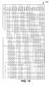
- FIG. 10is a truth table illustrating exemplary decoder logic for generating byte select drain and byte select ground switching signals in accordance with the invention.
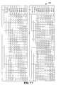
- FIG. 11is a truth table illustrating exemplary decoder logic for generating byte select precharge switching signals in accordance with the invention
- FIG. 12is a truth table illustrating exemplary decoder logic for generating column select switching signals in accordance with the invention.
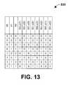
- FIG. 13is a truth table illustrating exemplary decoder logic for generating sector select switching signals in accordance with the invention.
- FIG. 14is a flow diagram illustrating an exemplary method of reading a memory cell in accordance with another aspect of the invention.
- the present inventionrelates to methods and apparatus for reading memory cells in a virtual ground architecture memory device, wherein adjacent cell leakage currents and the adverse effects associated therewith are mitigated or avoided by precharging such adjacent cells during a memory read operation.
- the inventionprovides decoder circuitry and methodologies by which appropriate connection of a target cell to a read voltage and ground, as well as of an adjacent cell to a precharge voltage are facilitated.
- the invention as illustrated and described hereinafterfinds particular utility in association with virtual ground memory devices employing dual bit type memory cells. However, it will be understood that the various aspects of the invention are also applicable to other devices, such as those having single bit cells.
- the inventionmay be employed for memory cell read operations using drain-side sensing as well as those employing source-side sensing.
- FIG. 1illustrates an exemplary dual bit memory cell 2 in association with which one or more of the various aspects of the invention may be carried out.
- the memory cell 2comprises, for example, a silicon nitride layer 3 with buried polysilicon islands (not numerically designated) therein.
- a P-type substrate 4has buried N+ source 5 and N+ drain 6 regions.
- the silicon nitride 3is sandwiched between two layers of silicon dioxide 7 and 8 .
- the layer 3may comprise any other form of charge trapping layer.
- Overlying the oxide layer 7is a polysilicon gate 9 . This gate 9 is doped with an N-type impurity (e.g., phosphorus).
- the memory cell 2is capable of storing two data bits, a left bit represented by the dashed circle A and a right bit represented by the dashed circle B.
- the dual bit memory cell 2is generally symmetrical, thus the drain 6 and the source 5 are interchangeable.
- the left junction 5may serve as the source terminal and the right junction 6 as the drain terminal with respect to the right bit B.
- the right junction 6may serve as the source terminal and the left junction 5 as the drain terminal for the left bit A.
- the memory read features and other aspects of the present inventionmay be implemented in association with various types of dual bit memory cell architectures, including the cell architecture of FIG. 1 as well as others not illustrated.
- the inventionis applicable to such dual bit memory devices wherein both bits (e.g., bits A and B of cell 2 ) are used for data or information storage, as well as those in which only one bit (e.g., bit A of cell 2 ) of the dual bit cell is so used.
- the inventionis applicable in association with single bit memory cells (not shown) organized in virtual ground type configurations in a memory device.
- a “virtual ground” architecture 100comprising rows 140 of flash cells 110 with stacked gate terminals 115 coupled to an associated word line (e.g., WL 0 thru WL n ) 140 , and columns (e.g., 160 , 170 , 180 , 190 ) of flash cell pairs (e.g., 110 & 130 ) with a drain 135 of one transistor 130 coupled to an associated bit line (e.g., BL 0 thru BL m ) and the source 120 of the adjacent transistor 110 as well.
- word linee.g., WL 0 thru WL n
- columnse.g., 160 , 170 , 180 , 190
- flash cell pairse.g., 110 & 130
- bit linee.g., BL 0 thru BL m
- each single row of flash cells(e.g., 110 & 130 ) associated with a word line 140 is connected in series, with the source 120 of one cell 110 coupled to the drain 135 of an adjacent cell 130 , wherein each drain terminal of the transistors within a single column is connected to the same bit line.
- Individual flash cellsmay be selected via the word line and a pair of bit lines bounding the associated cell.
- a positive voltageis applied to the bit line (BL 0 ) 160 coupled to the drain 125 of the flash cell 110
- a conductive pathis established between the drain 125 and the source 120 thereof, which is coupled to the bit line (BL 1 ) 170 and to ground (V SS ).
- V SSground
- a virtual groundis formed by selectively connecting a ground to the bit line associated with the source terminal of only those selected flash cells which are to be programmed or read.
- FIG. 3illustrates a single sector or IO 200 of virtual ground configuration flash memory cells 210 , wherein the IO 200 comprises both row decode logic circuits 220 for selecting one or more word lines 225 , and column decode logic circuits 230 for selecting two or more bit lines 235 .
- the array IO 200comprises, for example, 512 rows and 64 columns of memory cells 210 , which are associated with 512 word lines 225 and 64 bit lines 235 , respectively.
- a full memory array 250may comprise 16 such IOs 260 and 270 (e.g., similar to IO 200 of FIG. 3) with associated word line and bit line decode logic (not shown).
- a typical exemplary flash memory circuit 300is shown in FIG.
- the flash array 340comprises one or more sectors (e.g., 512 rows and 64 olumns) of memory cells, which are associated with an equivalent number of word lines and bit lines.
- the circuitry to read the flash cells in the virtual ground circuit 300includes a conventional global precharge circuit 360 to precharge all the bit lines of one or more sectors of the array with the same positive voltage V D (e.g., about 1.2 volts) 345 , which is used to sense the flash cell current of a specified cell via a cascode current-to-voltage preamplifier circuit 370 .
- the circuit 370supplies the positive voltage V D generated from the V CC 315 to a bit line on the drain side of the selected flash cell within the array 340 , while the source side of the selected cell is coupled thru another bit line to the ground 380 via the virtual ground switch circuitry 390 to generate a core cell sense current I CORE 375 .
- the cascode preamplifier circuit 370converts the core cell sense current I CORE 375 to a core cell sense voltage V CORE 377 for use in a sense amplifier 376 .
- the cascode preamplifier 370also generates a reference current I REF and converts this to a reference voltage V REF 378 , which is compared to V CORE 377 in the sense amplifier 376 .
- the sense voltage V CORE 377 associated with the flash cell sense current I CORE 375is compared to the reference voltage V REF 377 in the sense amplifier 376 to produce a core cell verification signal 379 indicative of the logical state (e.g., “1” or “0”) stored at the desired location.
- FIG. 6shows a conventional method 400 and four basic steps ( 410 , 420 , 430 , 440 ) for reading a selected flash cell in the virtual ground circuit of FIG. 5 .
- all bit lines(BL 0 thru BL M ) are first precharged to the same positive voltage V D (e.g., about 1.2 volts) as is used to sense the flash cell current.
- V Dpositive voltage
- the bit linesare assumed to be precharged to a positive voltage V D .
- the global precharge circuit voltage V Dis then disconnected from all the bit lines at time t 1 420 , and the bit lines are allowed to float without an applied voltage.
- a core cell 435is selected with a bit line BL X 436 at the drain side of the cell, an adjacent bit line BL X+1 445 at the source side of the cell, and a word line WL X coupled to the gate of the cell 435 to be sensed, while all other bit lines continue to float.
- the bit line BL X+1 445is selectively coupled as a virtual ground to ground 447 .
- the flash cell 435 sensing operation 448begins with the application of a word line voltage at WL X , a bit line voltage V D (e.g., drain read voltage) at 436 to the drain, and a ground 447 to the source 445 of the selected flash cell 435 .
- V Dbit line voltage
- Individual flash cellmay thus be selected via a word line and a pair of bit lines bounding the associated cell.
- a conduction pathis established when a positive voltage V D is applied to one of the bit lines (e.g., BL X ) 436 coupled to the drain of a flash cell, the source of the flash cell is coupled to an adjacent bit line (e.g., BL X+1 ) 445 , which is selectively coupled to ground (V SS ) 447 , and an appropriate word line (e.g., WL X ) voltage is applied to the gate of the selected cell.
- the core cell sense current 448is converted to a cell sense voltage V CORE within the cascode current-to-voltage preamplifier circuit along with a reference cell voltage V REF which is passed to a sense amplifier (e.g., amplifier 376 of FIG. 5) to produce a core cell verification signal (e.g., signal 379 of FIG. 5 ), which is indicative of the data stored in the flash core cell.
- a sense amplifiere.g., amplifier 376 of FIG. 5
- a core cell verification signale.g., signal 379 of FIG. 5
- the techniques illustrated in FIGS. 5 and 6suffer from leakage currents associated with cells neighboring the cell being read.
- the current I CORE which is sensed by the cascode preamplifier circuit 370 of FIG. 5includes the current flowing through the target cell being read, as well as leakage current flowing into the adjacent cell (e.g., the cell connected to the same bitline as the drain of the target cell).
- the circuit and method of FIGS. 5 and 6are prone to erroneous indications of the actual data stored in the target cell due to the leakage current effect. For instance, where the actual current flowing through the target cell is insufficient to generate a voltage V CORE greater than the reference voltage V REF , the addition of such leakage current to the sensed current I CORE may result in a V CORE reading above V REF .
- the circuitry of FIG. 5employs drain-side current sensing, wherein the cascode preamplifier circuit 350 senses the cell current between the drain of the target cell in the array 340 and the read voltage.
- Source-side sensing(not shown) can also be employed, wherein the target cell current is sensed between the target cell source and ground (e.g., between the column decode bitlines 350 and virtual ground 390 in FIG. 5 ).
- adjacent or neighboring cell leakage currentscan adversely affect the read operation in source-side sensing architectures.
- current from the target cell source in a source-side sensing configurationwill flow through the current sensor to the virtual ground, but may also flow into the drain of the adjacent cell (e.g., into the drain of the adjacent cell connected to the source of the target cell).
- the measured currentmay be less than the actual target cell current, causing the potential for a false data read operation.
- the present inventionaddresses the above and other problems in virtual ground type memory structures, facilitating stable, low power means of eliminating the effects of charge sharing leakage currents to adjacent and/or neighboring cells and loss in transient sense current during memory cell current read operations, resulting in substantially improved signal margins in a virtual ground flash memory array system.
- the inventionprovides decoder circuitry and techniques by which adjacent cells are precharged to avoid or mitigate leakage currents associated therewith during a read operation.
- the adjacent cell prechargingmay be performed prior to or simultaneously with the provision of a read voltage and virtual ground to the target cell, and the read operation may include multiple phases.
- the inventionprovides for precharging of the appropriate adjacent core memory cell to mitigate leakage current effects in drain-side sensing configurations, as well as for source-side sensing.
- the inventionis applicable in memory devices employing single bit cells and/or devices having multiple-bit (e.g., dual bit) memory cells.
- the inventionrelates to virtual ground flash memory decoder circuitry and methodologies for reading a flash memory cell in a virtual ground flash memory read operation.
- the systemcomprises a charge and hold circuit which is operable to apply a precharge voltage (e.g., about 1.2 volts) to a bit line of the cell of the flash array adjacent to the target cell, wherein the precharge voltage is substantially the same as the drain read voltage (e.g., about 1.2 volts) applied to the bit line of the sensed cell.
- a precharge voltagee.g., about 1.2 volts
- the systemalso provides decoding apparatus to select the bit lines of a target memory cell to be read and the bit line of an adjacent cell during memory read operations, wherein applying substantially the same voltage to the bit line of the cell adjacent to the cell being sensed, reduces or mitigates the adverse effects of adjacent cell leakage current.
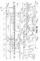
- the circuit 500comprises decoder circuitry 510 having row decode logic 520 for selecting one or more word lines 535 , and decoder circuitry 550 for selecting one or more bit lines 545 which are coupled to memory cell drain and source terminals within a virtual ground flash memory array 540 .
- the decoder circuitry 510decodes address lines 515 to generate the appropriate wordlines 535 via circuit 520 , and bitlines 547 via circuit 550 , whereby the appropriate cells in the memory array 540 can be accessed, such as in a read operation.
- rows of memory cellshave their gate terminals connected to a common wordline 535 , and the individual cells within such rows are selected by bitlines connected to the drain and source terminals thereof.
- the cells within a roware interconnected, wherein the source of one cell is connected to the drain of the adjacent cell, as well as to a bitline 547 .
- Individual bitlines 547are thus used to provide appropriate voltages to the drain and source of a target cell, while the wordlines 535 are used to provide appropriate gate voltages, in order to perform various operations (e.g., read, program, erase, verify, etc.) with respect to the array 540 .
- the array 540also comprises one or more sectors (e.g., 512 rows and 64 columns) of memory cells, which are associated with an equivalent number of word lines and bit lines.
- the decoder 510selectively connects the precharge voltage from the circuit 560 to a cell adjacent to the cell of interest during a read operation.
- the decoder 510also connects the drain and source of the target cell to a read voltage from circuit 570 and ground 580 , respectively, in order to generate and sense the cell current 575 associated therewith. In this manner, the data bit or bits in a cell can be read.
- the decoder circuitry of the inventioncan be employed in association with source-side sensing schemes as well.
- the circuit 500further includes a charge and hold circuit 560 providing a precharge voltage (e.g., a positive voltage V D 545 of about 1.2 volts) to the decoder 550 for selective application to a cell adjacent to the target cell in one or more sectors of the array 540 during a read operation, wherein the precharge voltage 545 is generated from V CC 515 .
- a precharge voltagee.g., a positive voltage V D 545 of about 1.2 volts
- a cascode current-to-voltage preamplifier circuit 570senses the target cell current by supplying virtually the same positive voltage V D (e.g., about 1.2 volts) 545 generated from the V CC 515 , via the decoder circuit 550 to a bit line on the drain side of the selected flash cell within the array 540 .
- the source side of the selected cellis coupled thru another bit line via the decoder 550 to the ground 580 to generate a core cell sense current I CORE 575 .
- the circuit 570converts the current I CORE 575 to a core cell sense voltage V CORE 577 for use in a sense amplifier 576 .
- the preamplifier 570also generates a reference current I REF (not shown) and converts this to a reference voltage V REF 578 , which is compared to V CORE 577 by the amplifier 576 .
- the sense voltage V CORE 577is compared to the reference voltage V REF 577 in the sense amplifier 576 to produce a core cell signal 579 indicative of the data in the target cell being read.
- drain-side sensingis employed in association with dual bit memory cells in a flash memory device 600 .
- the device 600comprises first, second, third, and fourth MOS type dual bit cells 601 , 602 , 603 , and 604 , respectively, having gate, drain, and source terminals.
- the gate terminals of the cells 601 , 602 , 603 , and 604are tied to a common wordline 605 , and the device 600 further comprises first, second, third, and fourth bitlines 611 , 612 , 613 , and 614 , respectively, wherein the drain terminal 620 of cell 601 is connected to bitline 611 .
- the source terminal 621 of cell 601 and the drain 622 of cell 602are connected to the second bitline 612 .
- the third bitline 613is connected to the source 623 of cell 602 and the drain 624 of the third cell 603 .
- the device 600comprises other cells (not shown) in the row having gates connected to the wordline 605 and associated bitlines therebetween connected to the drain of one cell and the source of an adjacent cell in a virtual ground configuration.
- a decoder circuit 630comprises first, second, and third switches 640 , 650 , and 660 , respectively, each comprising a byte select switch 670 , a column select switch 671 , and a sector select switch 672 , arranged in series.
- the three switches 670 , 671 , and 672 of the first switch 640conduct in order to connect the first bitline 611 with a precharge voltage 674 .
- the three switches 670 , 671 , and 672 of the second switch 650are turned on so as to connect the second bitline 612 to a read voltage 675 through a current sensor 676 , and the three switches 670 , 671 , and 672 of the third switch 660 conduct in order to connect the third bitline 613 to ground.
- the decoder 630thus operates to precharge the first cell 601 during a read operation associated with the second cell 602 , wherein current I CORE through the target cell 602 flows from the read voltage 675 through the current sensor 676 and the cell 602 to ground by virtue of the second and third switches 650 and 660 , respectively.
- the decoder 630can comprise arrays or groups of multiple such byte select, column select, and sector select switches 670 , 671 , and 672 , which are selectively activated by decoder signals (not shown) to form the first, second, and third switches 640 , 650 , and 660 .
- leakage currentcould flow from the read voltage 675 and into the cell 601 , resulting in the possibility of an erroneous sensing by the current sensor 676 , since such leakage current and the cell current I CORE are additive in the illustrated drain-side sensing configuration.
- the additive relationship between the desired cell current from cell 602 and the leakage current associated with adjacent cell 601results from the employment of drain-side sensing in the device 600 , where the current sensor 676 is connected between the bitline 612 and the read voltage 675 via the second switch 640 .
- the inventionmitigates or overcomes this shortcoming by providing the precharge voltage to the adjacent cell 601 via the decoder 630 so as to reduce or eliminate such leakage current during the read operation.
- the inventioncan be employed to mitigate adjacent cell leakage current effects where source-side current sensing is used.
- the current sensor 767is connected between the third bitline 613 and ground via the third switch 660 to sense the current I CORE through the second cell 602 during a read operation associated with the bit 5 of the cell 602 .
- the second switch 650is employed to connect the second bitline 612 to the read voltage 675 .
- leakage current from the first cell 601will not affect the current I CORE since the current associated with the cell 602 is being sensed on the source side. Rather, any leakage current from the other adjacent cell 603 can affect the reading of cell 602 .
- the inventionto provides for connecting the precharge voltage 674 to the fourth bitline 614 via a fourth decoder switch 680 comprising a byte select switch 670 , a column select switch 671 , and a sector select switch 672 .
- the precharge voltage 674is advantageously ground, so as to effectively short the adjacent cell 603 , thus preventing current from the target cell 602 from conducting through the adjacent cell 603 , as well as preventing current from the adjacent cell 603 from flowing through the third switch 660 and into the current sensor 676 .
- Precharging the adjacent cell 603thus reduces or mitigates the leakage current from the third cell 603 so as to provide improved read operation in the device 600 with respect to bit 5 of the target cell 602 .
- FIG. 8 cAnother variant is illustrated in FIG. 8 c , wherein a read operation is performed to ascertain the data in another bit (e.g., bit 4 ) of the second cell 602 using drain-side sensing.
- the second switch 650 of the decoder circuit 630connects the second bitline 612 (e.g., and hence the drain terminal 622 of the second cell 602 ) to ground, and the third switch 660 connects the third bitline 613 (e.g., and hence the source terminal 623 of the cell 602 ) to the read voltage 675 through the current sensor 676 .
- the other bite.g., bit 4
- the drain terminal 622is grounded while the source terminal 623 is brought to the read voltage through the current sensor 676 .
- drain-side sensingis used herein to refer to sensing current on the read voltage side of the cell
- source-side sensingrefers to sensing cell current on the ground side of the cell, although the drain and source terminals may be alternatively used depending upon which bit of a dual bit cell is being accessed. It will be noted that unlike the situation in FIG. 8 a , leakage current associated with cell 601 in FIG. 8 c does not affect the current I CORE . Rather, leakage current into the drain terminal 624 of the adjacent cell 603 could result in erroneous reading of the data in bit 4 of the target cell 602 .
- the inventionprovides for connection of the precharge voltage 674 to the fourth bitline 614 using the fourth switch 680 , thereby effectively shorting the adjacent cell 603 . This reduces or mitigates the leakage current associated with the cell 603 , whereby improved read operation can be achieved.
- FIG. 8 dYet another variation is illustrated in FIG. 8 d , wherein source-side sensing is used to read the second bit (e.g., bit 4 ) of the dual bit second memory cell 602 .
- the first switch 640 of the decoder 630connects the first bitline 611 to the precharge voltage 674 (e.g., ground, to short the adjacent cell 601 ) in order to mitigate leakage current associated with the first cell 601 .
- the second switch 650connects the second bitline 612 to ground through the current sensor 676
- the third switch 660connects the third bitline 613 to the read voltage 675 . Comparing FIGS.
- the decoder 630can be used to mitigate or overcome problems associated with adjacent cell leakage current in any situation involving single bit or multiple-bit cells using source or drain-side sensing in a virtual ground memory structure.
- FIG. 9 aanother exemplary implementation of the present invention further illustrates various features of the invention.
- a portion of a memory device 700is illustrated comprising a row of memory cells 702 , wherein the device 700 comprises many such rows and only a single row is illustrated for the sake of clarity.
- the individual memory cells 702are a dual bit type, wherein each such cell can store two data bits of information. For purposes of illustration, bit numbers for several such data bits are located near some of the illustrated cells 702 for reference in the following description.
- one such cell 703is able to store bits 4 and 5 , with a drain terminal connected to a local bitline 704 and a source terminal connected to another local bitline 705 .
- the gates of all the cells 703 in the roware connected to a common wordline 706 .
- decoder circuitry in the device 700comprises a byte select switch array 710 having four byte select switch groups 711 a - 711 d individually associated with corresponding global bitlines 712 a - 712 d .
- the byte select switch groups 711 a - 711 dindividually comprise a byte select drain switch transistor switched according to a byte select drain signal BSDv(x), which is connected between a drain read voltage terminal DATAB( 0 ) and an associated global bitline, a byte select ground switch transistor controlled by a byte select ground signal BSG(x), connected between ground and the associated global bitline, and a byte select precharge switch connected between a precharge voltage terminal DATAB 13 PRE and the associated global bitline, which is actuated by a byte select precharge signal BSPv(x).
- drain-side sensingis employed, wherein a current sensor (not shown) is situated between the read voltage terminal DATAB( 0 ) and a read voltage source (not shown).
- One byte select switch group 711 bcomprises a first transistor 711 b 1 connected between DATAB( 0 ) and the global bitline 712 b and controlled by a signal BSDv( 1 ), a second transistor 711 b 2 connected between the global bitline 712 b and ground and controlled by a signal BSG( 1 ), and a third transistor 711 b 3 connected between the global bitline 712 b and DATAB_PRE.
- the exemplary decoder of device 700activates one of the three transistors 711 b 1 , 711 b 2 , and 711 b 3 during a read operation in order to selectively connect the global bitline 712 b to one of ground, a precharge voltage (e.g., terminal DATAB_PRE), and a read voltage (e.g., DATAB( 0 )).
- a precharge voltagee.g., terminal DATAB_PRE
- a read voltagee.g., DATAB( 0 )
- the device 700further comprises intermediate bitlines MBLv(y), and the decoder circuitry provides a column select switch array 714 comprising a plurality of column select switch transistors 715 a - 715 h switching according to signals CS( 0 )-CS( 7 ), respectively.
- the column select transistor switches 715are located between an associated global bitline and an intermediate bitline so as to selectively provide connection therebetween according to the column select decoder signals CS.
- column select switch transistor 715 bis connected between global bitline 712 b and intermediate bitline MBLv( 1 ) to selectively connect the bitlines 712 b and MBLv( 1 ) according to the decoder signal CS( 1 ).
- column select transistor 715 fselectively connects the global bitline 712 b with intermediate bitline MBLv( 5 ) according to signal CS( 5 ).
- the memory device 700comprises a sector select switch array 720 comprising sector select switches or transistors 721 a - 721 p individually connected between an associated intermediate bitline MBLv(y) and an associated local bitline.
- the sector select transistor 721 cconnects the intermediate bitline MBLv( 1 ) with the local bitline 704 at the drain terminal of the memory cell 703 according to a sector select decoder signal SELn( 2 ).
- the decoderprovides the signals (e.g., BSDv(x), BSG(x), and BSPv(x)) to the byte select switches 711 , signals CS to the column select switches 715 , and signals SELn(i) to the sector select switches 721 , according to address lines (not shown) in a read operation.
- the decoder signalsthus provide appropriate interconnections via the switches 711 , 715 , and 721 in order to read a first memory cell (e.g., cell 703 ) and to precharge a second (e.g., adjacent) memory cell in the memory core during a read operation.
- the decoder of the memory device 700comprises the above switching devices and logic circuitry providing the switching signals for operation of the appropriate switches 711 , 715 , and 721 to read a cell and precharge an adjacent cell.
- a truth table 800illustrates the decoding of address lines A 0 -A 6 to provide the byte select drain signals BSDv(x) and the byte select ground signals BSG(x) for the switches 711 of the device 700 .
- a truth table 810illustrates the logical decoding of the address lines A 0 -A 6 to generate the byte select precharge decoder signals BSPv(x) for the switches 711 .
- FIG. 12illustrates the decoding of address lines A 0 -A 5 to provide the column select decoder signals CS for the switches 715
- FIG. 13illustrates a table 830 for decoding address lines A 0 -A 2 to generate the sector select control signals SELn(i) for the switches 721 .
- FIG. 9 billustrates a read operation in the memory device 700 , wherein a first data bit (e.g., bit 5 ) of cell 703 is read.
- the decoder signalsare applied to the appropriate byte select, column select, and sector select transistor switches 711 , 715 , and 721 , respectively, in order to connect local bitline 704 (e.g., and hence the drain of the target cell 703 ) to the read voltage through terminal DATAB( 0 ).
- the decoderconnects the source terminal (e.g., local bitline 705 ) to ground, and connects a local bitline 707 associated with a drain terminal of an adjacent cell 708 to a precharge voltage via the DATAB_PRE terminal, as indicated by the non-directional dashed lines in FIG. 9 b .
- Drain-side sensingis employed to sense the resulting cell current through the target cell 703 along the conduction path indicated by the bold dashed directional lines in FIG. 9 b . In this fashion, a determination is made as to the data stored in bit 5 of the cell 703 while reducing or mitigating leakage current effects associated with the adjacent memory cell 708 .
- the decoderprovides a byte select switching control signal BSDv( 1 ) to a byte select transistor 711 b 1 to connect the global bitline 712 b to the read voltage via terminal DATAB( 0 ), a signal BSG( 2 ) to a byte select transistor 711 c 1 to connect global bitline 712 c to ground, and a signal BSPv( 0 ) to transistor 711 a 1 to connect the global bitline 712 a to the precharge voltage (e.g., DATAB_PRE).
- BSDv( 1 )to a byte select transistor 711 b 1 to connect the global bitline 712 b to the read voltage via terminal DATAB( 0 )
- BSG( 2 )to a byte select transistor 711 c 1 to connect global bitline 712 c to ground
- a signal BSPv( 0 ) to transistor 711 a 1to connect the global bitline 712 a to the precharge voltage (e.g.,
- the decoderfurther provides column select control signals CS( 0 )-CS( 2 ) to activate column select transistor switches 715 a - 715 c , respectively.
- the exemplary decoderfurther actuates column select transistor 715 d via signal CS( 3 ) in order to simplify the decoding, but that this transistor 715 d need not be activated to perform the desired read of bit 5 of cell 703 .
- the decoder fuirtherprovides for adjacent cell precharging where the other bit (e.g., bit 4 ) of the dual bit target cell 703 is read.
- the decoder signalsare applied to the appropriate byte select, column select, and sector select transistor switches 711 , 715 , and 721 , respectively, in order to connect local bitline 705 (e.g., and hence the source of the target cell 703 ) to the read voltage through terminal DATAB( 0 ).
- the decoderconnects the target cell drain terminal (e.g., local bitline 704 ) to ground, and connects a local bitline 717 associated with the drain terminal of an adjacent cell 718 to the precharge voltage, as indicated by the non-directional dashed lines in FIG. 9 c .
- Drain-side sensingis employed to sense the resulting target cell current along the conduction path indicated by the bold dashed directional lines in FIG. 9 c . In this fashion, a determination is made as to the data stored in bit 4 of the target memory cell 703 while reducing or mitigating leakage current effects associated with the adjacent cell 718 .
- the decoderprovides a byte select switching control signal BSDv( 2 ) to a byte select transistor 711 c 2 to connect the global bitline 712 c to the read voltage, a signal BSG( 1 ) to the byte select transistor 711 b 2 to connect global bitline 712 b to ground, and a signal BSPv( 3 ) to transistor 711 d 1 to connect the global bitline 712 d to the precharge voltage.
- the decoderfurther provides column select control signals CS( 1 )-CS( 3 ) to activate column select transistor switches 715 b - 715 d , respectively.
- the decoderfurther activates sector select transistors 712 a , 712 c , and 712 g via sector select decoder control signals SELn( 0 ), SELn( 2 ), and SELn( 6 ) in order to connect the intermediate bitlines MBLv( 3 ), MBLv( 1 ), and MBLv( 2 ) to local bitlines 717 , 704 , and 705 , respectively.
- the inventionprovides decoding for source-side sensing configurations as well as those employing drain-side sensing.
- the inventioncan be applied to multiple bit virtual ground architectures (e.g., employing the dual bit cells 702 of FIGS. 9 a - 9 c ), as well as to single bit cells in a virtual ground configuration.
- the inventioncan be employed in association with reading any type of virtual ground memory organization, in order to mitigate or avoid the adverse effect of adjacent or neighboring cell leakage current during memory read operations.
- FIG. 14another aspect of the invention involves methods for reading memory cells in a virtual ground memory device.
- One such method 900is illustrated in FIG. 14 in accordance with the invention. While the exemplary method 900 is illustrated and described herein as a series of acts or events, it will be appreciated that the present invention is not limited by the illustrated ordering of such acts or events, as some acts may occur in different orders and/or concurrently with other acts or events apart from those illustrated and/or described herein, in accordance with the invention. In addition, not all illustrated steps may be required to implement a methodology in accordance with the present invention. Moreover, it will be appreciated that the method 900 may be implemented in association with the apparatus and systems illustrated and described herein as well as in association with other systems not illustrated.
- the drain of the target cellis connected to a read voltage at 908 and the source terminal is connected to ground at 910 in order to cause a cell current to flow in the target cell.
- the cell currentis sensed and the target cell is determined at 914 according to the sensed cell current, whereafter the method 900 ends at 916 .
- the read voltagecan alternatively be connected to the target cell source at 908 and the drain can alternatively be grounded at 914 , depending on which bit is to be read.
- the precharging of an adjacent memory cellcan be performed prior to or simultaneously with the connection of the target cell terminals with the read voltage and ground in accordance with the present invention.
- the exemplary method 900 and other methods according to the inventionthus provide for precharging an adjacent cell in order to facilitate error-free reading of a target cell in a virtual ground memory array by mitigate the leakage current associated with such an adjacent cell.
Landscapes
- Engineering & Computer Science (AREA)
- Microelectronics & Electronic Packaging (AREA)
- Read Only Memory (AREA)
Abstract
Description
Claims (20)
Priority Applications (1)
| Application Number | Priority Date | Filing Date | Title |
|---|---|---|---|
| US09/928,059US6525969B1 (en) | 2001-08-10 | 2001-08-10 | Decoder apparatus and methods for pre-charging bit lines |
Applications Claiming Priority (1)
| Application Number | Priority Date | Filing Date | Title |
|---|---|---|---|
| US09/928,059US6525969B1 (en) | 2001-08-10 | 2001-08-10 | Decoder apparatus and methods for pre-charging bit lines |
Publications (1)
| Publication Number | Publication Date |
|---|---|
| US6525969B1true US6525969B1 (en) | 2003-02-25 |
Family
ID=25455655
Family Applications (1)
| Application Number | Title | Priority Date | Filing Date |
|---|---|---|---|
| US09/928,059Expired - LifetimeUS6525969B1 (en) | 2001-08-10 | 2001-08-10 | Decoder apparatus and methods for pre-charging bit lines |
Country Status (1)
| Country | Link |
|---|---|
| US (1) | US6525969B1 (en) |
Cited By (85)
| Publication number | Priority date | Publication date | Assignee | Title |
|---|---|---|---|---|
| US20040004247A1 (en)* | 2002-07-08 | 2004-01-08 | Micron Technology, Inc. | Memory utilizing oxide-nitride nanolaminates |
| US6700815B2 (en)* | 2002-04-08 | 2004-03-02 | Advanced Micro Devices, Inc. | Refresh scheme for dynamic page programming |
| US6738301B2 (en) | 2002-08-29 | 2004-05-18 | Micron Technology, Inc. | Method and system for accelerating coupling of digital signals |
| US20040105312A1 (en)* | 2002-12-02 | 2004-06-03 | Yi He | Pre-charge method for reading a non-volatile memory cell |
| US6768679B1 (en)* | 2003-02-10 | 2004-07-27 | Advanced Micro Devices, Inc. | Selection circuit for accurate memory read operations |
| US6771539B2 (en)* | 2001-05-09 | 2004-08-03 | Macronix International Co., Ltd. | Method for operating non-volatile memory with symmetrical dual-channels |
| US20040153620A1 (en)* | 2003-01-30 | 2004-08-05 | Shai Eisen | Address scramble |
| US6795342B1 (en)* | 2002-12-02 | 2004-09-21 | Advanced Micro Devices, Inc. | System for programming a non-volatile memory cell |
| US20040218426A1 (en)* | 2003-04-29 | 2004-11-04 | Oleg Dadashev | Apparatus and methods for multi-level sensing in a memory array |
| US6859392B2 (en) | 2002-08-26 | 2005-02-22 | Micron Technology, Inc. | Preconditioning global bitlines |
| EP1513160A1 (en)* | 2003-09-04 | 2005-03-09 | Macronix International Co., Ltd. | A non-volatile flash memory |
| US20050057953A1 (en)* | 2003-09-16 | 2005-03-17 | Eli Lusky | Reading array cell with matched reference cell |
| US6903970B2 (en)* | 2002-08-22 | 2005-06-07 | Micron Technology, Inc. | Flash memory device with distributed coupling between array ground and substrate |
| US6950344B1 (en)* | 2003-11-24 | 2005-09-27 | Advanced Micro Devices, Inc. | Reading flash memory |
| US20050232024A1 (en)* | 2004-04-19 | 2005-10-20 | Shahar Atir | Method for reading a memory array with neighbor effect cancellation |
| US6963505B2 (en) | 2002-10-29 | 2005-11-08 | Aifun Semiconductors Ltd. | Method circuit and system for determining a reference voltage |
| US20060008966A1 (en)* | 2002-07-08 | 2006-01-12 | Micron Technology, Inc. | Memory utilizing oxide-conductor nanolaminates |
| US6992932B2 (en) | 2002-10-29 | 2006-01-31 | Saifun Semiconductors Ltd | Method circuit and system for read error detection in a non-volatile memory array |
| US20060034122A1 (en)* | 2004-08-12 | 2006-02-16 | Yoram Betser | Dynamic matching of signal path and reference path for sensing |
| US20060056240A1 (en)* | 2004-04-01 | 2006-03-16 | Saifun Semiconductors, Ltd. | Method, circuit and system for erasing one or more non-volatile memory cells |
| US20060068551A1 (en)* | 2004-09-27 | 2006-03-30 | Saifun Semiconductors, Ltd. | Method for embedding NROM |
| US20060126382A1 (en)* | 2004-12-09 | 2006-06-15 | Eduardo Maayan | Method for reading non-volatile memory cells |
| US20060126396A1 (en)* | 2002-01-31 | 2006-06-15 | Saifun Semiconductors, Ltd. | Method, system, and circuit for operating a non-volatile memory array |
| US7064983B2 (en) | 2001-04-05 | 2006-06-20 | Saifum Semiconductors Ltd. | Method for programming a reference cell |
| US20060141642A1 (en)* | 2004-12-28 | 2006-06-29 | Dongbuanam Semiconductor Inc. | Method for making mask in process of fabricating semiconductor device |
| US20060146624A1 (en)* | 2004-12-02 | 2006-07-06 | Saifun Semiconductors, Ltd. | Current folding sense amplifier |
| US20060152975A1 (en)* | 2002-07-10 | 2006-07-13 | Eduardo Maayan | Multiple use memory chip |
| US20060158940A1 (en)* | 2005-01-19 | 2006-07-20 | Saifun Semiconductors, Ltd. | Partial erase verify |
| US20060211188A1 (en)* | 2004-10-14 | 2006-09-21 | Saifun Semiconductors Ltd. | Non-volatile memory structure and method of fabrication |
| JP2006310868A (en)* | 2005-04-29 | 2006-11-09 | Infineon Technologies Ag | Multi-bit virtual ground NAND memory device, memory device |
| US20060262598A1 (en)* | 1997-08-01 | 2006-11-23 | Saifun Semiconductors Ltd. | Two bit non-volatile electrically erasable and programmable semiconductor memory cell utilizing asymmetrical charge trapping |
| US20060285408A1 (en)* | 2005-06-17 | 2006-12-21 | Saifun Semiconductors, Ltd. | Method circuit and system for compensating for temperature induced margin loss in non-volatile memory cells |
| US20060285386A1 (en)* | 2005-06-15 | 2006-12-21 | Saifun Semiconductors, Ltd. | Accessing an NROM array |
| US20070002645A1 (en)* | 2005-06-30 | 2007-01-04 | Thomas Roehr | Method for programming multi-bit charge-trapping memory cell arrays |
| US20070002632A1 (en)* | 2005-06-30 | 2007-01-04 | Renesas Technology Corp. | Semiconductor storage device having memory cell for storing data by using difference in threshold voltage |
| US20070015331A1 (en)* | 2002-06-21 | 2007-01-18 | Micron Technology, Inc. | Nor flash memory cell with high storage density |
| US20070032016A1 (en)* | 2001-11-19 | 2007-02-08 | Saifun Semiconductors Ltd. | Protective layer in memory device and method therefor |
| US20070036007A1 (en)* | 2005-08-09 | 2007-02-15 | Saifun Semiconductors, Ltd. | Sticky bit buffer |
| US20070051982A1 (en)* | 2005-07-18 | 2007-03-08 | Saifun Semiconductors Ltd. | Dense non-volatile memory array and method of fabrication |
| US20070096199A1 (en)* | 2005-09-08 | 2007-05-03 | Eli Lusky | Method of manufacturing symmetric arrays |
| US7218563B1 (en)* | 2005-11-18 | 2007-05-15 | Macronix International Co., Ltd. | Method and apparatus for reading data from nonvolatile memory |
| US7221138B2 (en) | 2005-09-27 | 2007-05-22 | Saifun Semiconductors Ltd | Method and apparatus for measuring charge pump output current |
| US20070120180A1 (en)* | 2005-11-25 | 2007-05-31 | Boaz Eitan | Transition areas for dense memory arrays |
| US20070133276A1 (en)* | 2003-09-16 | 2007-06-14 | Eli Lusky | Operating array cells with matched reference cells |
| US20070141788A1 (en)* | 2005-05-25 | 2007-06-21 | Ilan Bloom | Method for embedding non-volatile memory with logic circuitry |
| US20070153575A1 (en)* | 2006-01-03 | 2007-07-05 | Saifun Semiconductors, Ltd. | Method, system, and circuit for operating a non-volatile memory array |
| US20070159880A1 (en)* | 2006-01-12 | 2007-07-12 | Boaz Eitan | Secondary injection for NROM |
| US20070168637A1 (en)* | 2003-01-31 | 2007-07-19 | Yan Polansky | Memory array programming circuit and a method for using the circuit |
| US20070173017A1 (en)* | 2006-01-20 | 2007-07-26 | Saifun Semiconductors, Ltd. | Advanced non-volatile memory array and method of fabrication thereof |
| US20070194835A1 (en)* | 2006-02-21 | 2007-08-23 | Alexander Kushnarenko | Circuit and method for powering up an integrated circuit and an integrated circuit utilizing same |
| US20070196982A1 (en)* | 2006-02-21 | 2007-08-23 | Saifun Semiconductors Ltd. | Nrom non-volatile mode of operation |
| US20070195607A1 (en)* | 2006-02-21 | 2007-08-23 | Saifun Semiconductors Ltd. | Nrom non-volatile memory and mode of operation |
| US7272060B1 (en)* | 2004-12-01 | 2007-09-18 | Spansion Llc | Method, system, and circuit for performing a memory related operation |
| US20070237003A1 (en)* | 2006-04-05 | 2007-10-11 | Ashot Melik-Martirosian | Flash memory programming and verification with reduced leakage current |
| US20070253255A1 (en)* | 2006-04-28 | 2007-11-01 | Girolamo Gallo | Memory device, method for sensing a current output from a selected memory cell and sensing circuit |
| US20070253248A1 (en)* | 2006-04-27 | 2007-11-01 | Eduardo Maayan | Method for programming a reference cell |
| US20070255889A1 (en)* | 2006-03-22 | 2007-11-01 | Yoav Yogev | Non-volatile memory device and method of operating the device |
| US20070285990A1 (en)* | 2006-06-10 | 2007-12-13 | Samsung Electronics Co., Ltd. | Semiconductor device and method for compensating voltage drop of a bit line |
| US7317633B2 (en) | 2004-07-06 | 2008-01-08 | Saifun Semiconductors Ltd | Protection of NROM devices from charge damage |
| US20080037336A1 (en)* | 2006-08-11 | 2008-02-14 | Kazuyuki Kouno | Semiconductor memory device |
| US20080062757A1 (en)* | 2002-06-21 | 2008-03-13 | Micron Technology, Inc. | Nanocrystal write once read only memory for archival storage |
| US20080080251A1 (en)* | 2006-09-29 | 2008-04-03 | Macronix International Co., Ltd. | Method of reading dual-bit memory cell |
| US20080084753A1 (en)* | 2006-09-25 | 2008-04-10 | Macronix International Co., Ltd. | Decoding method in an NROM flash memory array |
| US20080094127A1 (en)* | 2006-09-18 | 2008-04-24 | Yoram Betser | Measuring and controlling current consumption and output current of charge pumps |
| US20080170441A1 (en)* | 2007-01-12 | 2008-07-17 | Gabriele Pelli | Sense architecture |
| US20080186769A1 (en)* | 2007-02-07 | 2008-08-07 | Macronix International Co., Ltd. | Method for metal bit line arrangement |
| US20080239599A1 (en)* | 2007-04-01 | 2008-10-02 | Yehuda Yizraeli | Clamping Voltage Events Such As ESD |
| US20080247239A1 (en)* | 2007-04-05 | 2008-10-09 | Hao Thai Nguyen | Method for current sensing with biasing of source and p-well in non-volatile storage |
| US20080247241A1 (en)* | 2007-04-05 | 2008-10-09 | Hao Thai Nguyen | Sensing in non-volatile storage using pulldown to regulated source voltage to remove system noise |
| US7535765B2 (en) | 2004-12-09 | 2009-05-19 | Saifun Semiconductors Ltd. | Non-volatile memory device and method for reading cells |
| US20090129160A1 (en)* | 2006-03-03 | 2009-05-21 | Nima Mokhlesi | Read operation for non-volatile storage with compensation for coupling |
| WO2009075832A1 (en)* | 2007-12-11 | 2009-06-18 | Spansion Llc | Nonvolatile storage device and control method thereof |
| US7590001B2 (en) | 2007-12-18 | 2009-09-15 | Saifun Semiconductors Ltd. | Flash memory with optimized write sector spares |
| US7638835B2 (en) | 2006-02-28 | 2009-12-29 | Saifun Semiconductors Ltd. | Double density NROM with nitride strips (DDNS) |
| US7668017B2 (en) | 2005-08-17 | 2010-02-23 | Saifun Semiconductors Ltd. | Method of erasing non-volatile memory cells |
| US7675782B2 (en) | 2002-10-29 | 2010-03-09 | Saifun Semiconductors Ltd. | Method, system and circuit for programming a non-volatile memory array |
| US7728626B2 (en) | 2002-07-08 | 2010-06-01 | Micron Technology, Inc. | Memory utilizing oxide nanolaminates |
| US20110122721A1 (en)* | 2008-09-05 | 2011-05-26 | Macronix International Co., Ltd. | Y-Decoder and Decoding Method Thereof |
| US20110235412A1 (en)* | 2007-12-21 | 2011-09-29 | Spansion Llc | Controlling ac disturbance while programming |
| US8053812B2 (en) | 2005-03-17 | 2011-11-08 | Spansion Israel Ltd | Contact in planar NROM technology |
| US20120327717A1 (en)* | 2010-06-28 | 2012-12-27 | Spansion Llc | High read speed memory with gate isolation |
| TWI424443B (en)* | 2009-05-08 | 2014-01-21 | Macronix Int Co Ltd | Memory array and method of operating a memory |
| US20160293615A1 (en)* | 2015-04-06 | 2016-10-06 | SK Hynix Inc. | Nonvolatile memory cells, nonvolatile memory cell arrays including the same, and methods of fabricating the same |
| US20210375370A1 (en)* | 2020-05-28 | 2021-12-02 | Taiwan Semiconductor Manufacturing Company, Ltd. | System and method for reliable sensing of memory cells |
| US20230377661A1 (en)* | 2020-05-28 | 2023-11-23 | Taiwan Semiconductor Manufacturing Company, Ltd. | System and method for reliable sensing of memory cells |
Citations (3)
| Publication number | Priority date | Publication date | Assignee | Title |
|---|---|---|---|---|
| US6134156A (en)* | 1999-02-04 | 2000-10-17 | Saifun Semiconductors Ltd. | Method for initiating a retrieval procedure in virtual ground arrays |
| US6201737B1 (en) | 2000-01-28 | 2001-03-13 | Advanced Micro Devices, Inc. | Apparatus and method to characterize the threshold distribution in an NROM virtual ground array |
| US20020005547A1 (en)* | 2000-04-10 | 2002-01-17 | Kenji Hibino | Semiconductor memory apparatus and method for outputting data |
- 2001
- 2001-08-10USUS09/928,059patent/US6525969B1/ennot_activeExpired - Lifetime
Patent Citations (3)
| Publication number | Priority date | Publication date | Assignee | Title |
|---|---|---|---|---|
| US6134156A (en)* | 1999-02-04 | 2000-10-17 | Saifun Semiconductors Ltd. | Method for initiating a retrieval procedure in virtual ground arrays |
| US6201737B1 (en) | 2000-01-28 | 2001-03-13 | Advanced Micro Devices, Inc. | Apparatus and method to characterize the threshold distribution in an NROM virtual ground array |
| US20020005547A1 (en)* | 2000-04-10 | 2002-01-17 | Kenji Hibino | Semiconductor memory apparatus and method for outputting data |
Cited By (176)
| Publication number | Priority date | Publication date | Assignee | Title |
|---|---|---|---|---|
| US7405969B2 (en) | 1997-08-01 | 2008-07-29 | Saifun Semiconductors Ltd. | Non-volatile memory cell and non-volatile memory devices |
| US20090032862A1 (en)* | 1997-08-01 | 2009-02-05 | Eduardo Maayan | Non-volatile memory cell and non-volatile memory device using said cell |
| US20060262598A1 (en)* | 1997-08-01 | 2006-11-23 | Saifun Semiconductors Ltd. | Two bit non-volatile electrically erasable and programmable semiconductor memory cell utilizing asymmetrical charge trapping |
| US20080111177A1 (en)* | 1997-08-01 | 2008-05-15 | Eduardo Maayan | Non-volatile memory cell and non-volatile memory device using said cell |
| US7064983B2 (en) | 2001-04-05 | 2006-06-20 | Saifum Semiconductors Ltd. | Method for programming a reference cell |
| US6771539B2 (en)* | 2001-05-09 | 2004-08-03 | Macronix International Co., Ltd. | Method for operating non-volatile memory with symmetrical dual-channels |
| US20070032016A1 (en)* | 2001-11-19 | 2007-02-08 | Saifun Semiconductors Ltd. | Protective layer in memory device and method therefor |
| US20060126396A1 (en)* | 2002-01-31 | 2006-06-15 | Saifun Semiconductors, Ltd. | Method, system, and circuit for operating a non-volatile memory array |
| US7420848B2 (en) | 2002-01-31 | 2008-09-02 | Saifun Semiconductors Ltd. | Method, system, and circuit for operating a non-volatile memory array |
| US6700815B2 (en)* | 2002-04-08 | 2004-03-02 | Advanced Micro Devices, Inc. | Refresh scheme for dynamic page programming |
| US7476586B2 (en)* | 2002-06-21 | 2009-01-13 | Micron Technology, Inc. | NOR flash memory cell with high storage density |
| US20070015331A1 (en)* | 2002-06-21 | 2007-01-18 | Micron Technology, Inc. | Nor flash memory cell with high storage density |
| US7639528B2 (en) | 2002-06-21 | 2009-12-29 | Micron Technology, Inc. | Nanocrystal write once read only memory for archival storage |
| US20080062757A1 (en)* | 2002-06-21 | 2008-03-13 | Micron Technology, Inc. | Nanocrystal write once read only memory for archival storage |
| US7494873B2 (en) | 2002-07-08 | 2009-02-24 | Micron Technology, Inc. | Memory utilizing oxide-nitride nanolaminates |
| US20060008966A1 (en)* | 2002-07-08 | 2006-01-12 | Micron Technology, Inc. | Memory utilizing oxide-conductor nanolaminates |
| US7728626B2 (en) | 2002-07-08 | 2010-06-01 | Micron Technology, Inc. | Memory utilizing oxide nanolaminates |
| US7847344B2 (en) | 2002-07-08 | 2010-12-07 | Micron Technology, Inc. | Memory utilizing oxide-nitride nanolaminates |
| US8228725B2 (en) | 2002-07-08 | 2012-07-24 | Micron Technology, Inc. | Memory utilizing oxide nanolaminates |
| US7489545B2 (en) | 2002-07-08 | 2009-02-10 | Micron Technology, Inc. | Memory utilizing oxide-nitride nanolaminates |
| US20040004247A1 (en)* | 2002-07-08 | 2004-01-08 | Micron Technology, Inc. | Memory utilizing oxide-nitride nanolaminates |
| US20060258097A1 (en)* | 2002-07-08 | 2006-11-16 | Micron Technology, Inc. | Memory utilizing oxide-nitride nanolaminates |
| US7583534B2 (en) | 2002-07-08 | 2009-09-01 | Micron Technolgy, Inc. | Memory utilizing oxide-conductor nanolaminates |
| US20060261376A1 (en)* | 2002-07-08 | 2006-11-23 | Micron Technology, Inc. | Memory utilizing oxide-nitride nanolaminates |
| US20060152975A1 (en)* | 2002-07-10 | 2006-07-13 | Eduardo Maayan | Multiple use memory chip |
| US7738304B2 (en) | 2002-07-10 | 2010-06-15 | Saifun Semiconductors Ltd. | Multiple use memory chip |
| US6903970B2 (en)* | 2002-08-22 | 2005-06-07 | Micron Technology, Inc. | Flash memory device with distributed coupling between array ground and substrate |
| US6859392B2 (en) | 2002-08-26 | 2005-02-22 | Micron Technology, Inc. | Preconditioning global bitlines |
| US7120054B2 (en) | 2002-08-26 | 2006-10-10 | Micron Technology, Inc. | Preconditioning global bitlines |
| US20050141282A1 (en)* | 2002-08-26 | 2005-06-30 | Micron Technology, Inc. | Preconditioning global bitlines |
| US6738301B2 (en) | 2002-08-29 | 2004-05-18 | Micron Technology, Inc. | Method and system for accelerating coupling of digital signals |
| US20040196729A1 (en)* | 2002-08-29 | 2004-10-07 | Kirsch Howard C | Method and system for accelerating coupling digital signals |
| US6925019B2 (en) | 2002-08-29 | 2005-08-02 | Micron Technology, Inc. | Method and system for accelerating coupling of digital signals |
| US6963505B2 (en) | 2002-10-29 | 2005-11-08 | Aifun Semiconductors Ltd. | Method circuit and system for determining a reference voltage |
| US7675782B2 (en) | 2002-10-29 | 2010-03-09 | Saifun Semiconductors Ltd. | Method, system and circuit for programming a non-volatile memory array |
| US6992932B2 (en) | 2002-10-29 | 2006-01-31 | Saifun Semiconductors Ltd | Method circuit and system for read error detection in a non-volatile memory array |
| WO2004051663A1 (en)* | 2002-12-02 | 2004-06-17 | Advanced Micro Devices, Inc. | Improved pre-charge method for reading a non-volatile memory cell |
| US20040105312A1 (en)* | 2002-12-02 | 2004-06-03 | Yi He | Pre-charge method for reading a non-volatile memory cell |
| US6788583B2 (en) | 2002-12-02 | 2004-09-07 | Advanced Micro Devices, Inc. | Pre-charge method for reading a non-volatile memory cell |
| US6795342B1 (en)* | 2002-12-02 | 2004-09-21 | Advanced Micro Devices, Inc. | System for programming a non-volatile memory cell |
| US20040153620A1 (en)* | 2003-01-30 | 2004-08-05 | Shai Eisen | Address scramble |
| US6967896B2 (en) | 2003-01-30 | 2005-11-22 | Saifun Semiconductors Ltd | Address scramble |
| US20070168637A1 (en)* | 2003-01-31 | 2007-07-19 | Yan Polansky | Memory array programming circuit and a method for using the circuit |
| US7743230B2 (en) | 2003-01-31 | 2010-06-22 | Saifun Semiconductors Ltd. | Memory array programming circuit and a method for using the circuit |
| US6768679B1 (en)* | 2003-02-10 | 2004-07-27 | Advanced Micro Devices, Inc. | Selection circuit for accurate memory read operations |
| US7142464B2 (en) | 2003-04-29 | 2006-11-28 | Saifun Semiconductors Ltd. | Apparatus and methods for multi-level sensing in a memory array |
| US20040218426A1 (en)* | 2003-04-29 | 2004-11-04 | Oleg Dadashev | Apparatus and methods for multi-level sensing in a memory array |
| EP1513160A1 (en)* | 2003-09-04 | 2005-03-09 | Macronix International Co., Ltd. | A non-volatile flash memory |
| US7457183B2 (en) | 2003-09-16 | 2008-11-25 | Saifun Semiconductors Ltd. | Operating array cells with matched reference cells |
| US20050057953A1 (en)* | 2003-09-16 | 2005-03-17 | Eli Lusky | Reading array cell with matched reference cell |
| US20070133276A1 (en)* | 2003-09-16 | 2007-06-14 | Eli Lusky | Operating array cells with matched reference cells |
| US6954393B2 (en)* | 2003-09-16 | 2005-10-11 | Saifun Semiconductors Ltd. | Reading array cell with matched reference cell |
| US7864612B2 (en) | 2003-09-16 | 2011-01-04 | Spansion Israel Ltd | Reading array cell with matched reference cell |
| US6950344B1 (en)* | 2003-11-24 | 2005-09-27 | Advanced Micro Devices, Inc. | Reading flash memory |
| US7532529B2 (en) | 2004-03-29 | 2009-05-12 | Saifun Semiconductors Ltd. | Apparatus and methods for multi-level sensing in a memory array |
| US20060056240A1 (en)* | 2004-04-01 | 2006-03-16 | Saifun Semiconductors, Ltd. | Method, circuit and system for erasing one or more non-volatile memory cells |
| US7652930B2 (en) | 2004-04-01 | 2010-01-26 | Saifun Semiconductors Ltd. | Method, circuit and system for erasing one or more non-volatile memory cells |
| US7755938B2 (en) | 2004-04-19 | 2010-07-13 | Saifun Semiconductors Ltd. | Method for reading a memory array with neighbor effect cancellation |
| US20050232024A1 (en)* | 2004-04-19 | 2005-10-20 | Shahar Atir | Method for reading a memory array with neighbor effect cancellation |
| US7317633B2 (en) | 2004-07-06 | 2008-01-08 | Saifun Semiconductors Ltd | Protection of NROM devices from charge damage |
| US7466594B2 (en) | 2004-08-12 | 2008-12-16 | Saifun Semiconductors Ltd. | Dynamic matching of signal path and reference path for sensing |
| US20070171717A1 (en)* | 2004-08-12 | 2007-07-26 | Saifun Semiconductors Ltd. | Dynamic matching of signal path and reference path for sensing |
| US7095655B2 (en) | 2004-08-12 | 2006-08-22 | Saifun Semiconductors Ltd. | Dynamic matching of signal path and reference path for sensing |
| US20060034122A1 (en)* | 2004-08-12 | 2006-02-16 | Yoram Betser | Dynamic matching of signal path and reference path for sensing |
| US20060068551A1 (en)* | 2004-09-27 | 2006-03-30 | Saifun Semiconductors, Ltd. | Method for embedding NROM |
| US7964459B2 (en) | 2004-10-14 | 2011-06-21 | Spansion Israel Ltd. | Non-volatile memory structure and method of fabrication |
| US20060211188A1 (en)* | 2004-10-14 | 2006-09-21 | Saifun Semiconductors Ltd. | Non-volatile memory structure and method of fabrication |
| US7638850B2 (en) | 2004-10-14 | 2009-12-29 | Saifun Semiconductors Ltd. | Non-volatile memory structure and method of fabrication |
| US7272060B1 (en)* | 2004-12-01 | 2007-09-18 | Spansion Llc | Method, system, and circuit for performing a memory related operation |
| US20060146624A1 (en)* | 2004-12-02 | 2006-07-06 | Saifun Semiconductors, Ltd. | Current folding sense amplifier |
| US20060126382A1 (en)* | 2004-12-09 | 2006-06-15 | Eduardo Maayan | Method for reading non-volatile memory cells |
| US7535765B2 (en) | 2004-12-09 | 2009-05-19 | Saifun Semiconductors Ltd. | Non-volatile memory device and method for reading cells |
| US7257025B2 (en) | 2004-12-09 | 2007-08-14 | Saifun Semiconductors Ltd | Method for reading non-volatile memory cells |
| US20060141642A1 (en)* | 2004-12-28 | 2006-06-29 | Dongbuanam Semiconductor Inc. | Method for making mask in process of fabricating semiconductor device |
| US7437702B2 (en)* | 2004-12-28 | 2008-10-14 | Dongbuanam Semiconductor, Inc. | Method for making mask in process of fabricating semiconductor device |
| US7468926B2 (en) | 2005-01-19 | 2008-12-23 | Saifun Semiconductors Ltd. | Partial erase verify |
| US20060158940A1 (en)* | 2005-01-19 | 2006-07-20 | Saifun Semiconductors, Ltd. | Partial erase verify |
| US7369440B2 (en) | 2005-01-19 | 2008-05-06 | Saifun Semiconductors Ltd. | Method, circuit and systems for erasing one or more non-volatile memory cells |
| US8053812B2 (en) | 2005-03-17 | 2011-11-08 | Spansion Israel Ltd | Contact in planar NROM technology |
| JP2006310868A (en)* | 2005-04-29 | 2006-11-09 | Infineon Technologies Ag | Multi-bit virtual ground NAND memory device, memory device |
| US20070141788A1 (en)* | 2005-05-25 | 2007-06-21 | Ilan Bloom | Method for embedding non-volatile memory with logic circuitry |
| US8400841B2 (en) | 2005-06-15 | 2013-03-19 | Spansion Israel Ltd. | Device to program adjacent storage cells of different NROM cells |
| US20060285386A1 (en)* | 2005-06-15 | 2006-12-21 | Saifun Semiconductors, Ltd. | Accessing an NROM array |
| US20060285408A1 (en)* | 2005-06-17 | 2006-12-21 | Saifun Semiconductors, Ltd. | Method circuit and system for compensating for temperature induced margin loss in non-volatile memory cells |
| US7184317B2 (en)* | 2005-06-30 | 2007-02-27 | Infineon Technologies Ag | Method for programming multi-bit charge-trapping memory cell arrays |
| US20070002645A1 (en)* | 2005-06-30 | 2007-01-04 | Thomas Roehr | Method for programming multi-bit charge-trapping memory cell arrays |
| US20070002632A1 (en)* | 2005-06-30 | 2007-01-04 | Renesas Technology Corp. | Semiconductor storage device having memory cell for storing data by using difference in threshold voltage |
| US7719900B2 (en)* | 2005-06-30 | 2010-05-18 | Renesas Technology Corp. | Semiconductor storage device having memory cell for storing data by using difference in threshold voltage |
| US7786512B2 (en) | 2005-07-18 | 2010-08-31 | Saifun Semiconductors Ltd. | Dense non-volatile memory array and method of fabrication |
| US20070051982A1 (en)* | 2005-07-18 | 2007-03-08 | Saifun Semiconductors Ltd. | Dense non-volatile memory array and method of fabrication |
| US20070036007A1 (en)* | 2005-08-09 | 2007-02-15 | Saifun Semiconductors, Ltd. | Sticky bit buffer |
| US7668017B2 (en) | 2005-08-17 | 2010-02-23 | Saifun Semiconductors Ltd. | Method of erasing non-volatile memory cells |
| US20070096199A1 (en)* | 2005-09-08 | 2007-05-03 | Eli Lusky | Method of manufacturing symmetric arrays |
| US7221138B2 (en) | 2005-09-27 | 2007-05-22 | Saifun Semiconductors Ltd | Method and apparatus for measuring charge pump output current |
| US20070115737A1 (en)* | 2005-11-18 | 2007-05-24 | Macronix International Co. Ltd. | Method and apparatus for reading data from nonvolatile memory |
| US7218563B1 (en)* | 2005-11-18 | 2007-05-15 | Macronix International Co., Ltd. | Method and apparatus for reading data from nonvolatile memory |
| US20070120180A1 (en)* | 2005-11-25 | 2007-05-31 | Boaz Eitan | Transition areas for dense memory arrays |
| US7352627B2 (en) | 2006-01-03 | 2008-04-01 | Saifon Semiconductors Ltd. | Method, system, and circuit for operating a non-volatile memory array |
| US20070153575A1 (en)* | 2006-01-03 | 2007-07-05 | Saifun Semiconductors, Ltd. | Method, system, and circuit for operating a non-volatile memory array |
| US7808818B2 (en) | 2006-01-12 | 2010-10-05 | Saifun Semiconductors Ltd. | Secondary injection for NROM |
| US20070159880A1 (en)* | 2006-01-12 | 2007-07-12 | Boaz Eitan | Secondary injection for NROM |
| US20070173017A1 (en)* | 2006-01-20 | 2007-07-26 | Saifun Semiconductors, Ltd. | Advanced non-volatile memory array and method of fabrication thereof |
| US8253452B2 (en) | 2006-02-21 | 2012-08-28 | Spansion Israel Ltd | Circuit and method for powering up an integrated circuit and an integrated circuit utilizing same |
| US20070194835A1 (en)* | 2006-02-21 | 2007-08-23 | Alexander Kushnarenko | Circuit and method for powering up an integrated circuit and an integrated circuit utilizing same |
| US7692961B2 (en) | 2006-02-21 | 2010-04-06 | Saifun Semiconductors Ltd. | Method, circuit and device for disturb-control of programming nonvolatile memory cells by hot-hole injection (HHI) and by channel hot-electron (CHE) injection |
| US7760554B2 (en) | 2006-02-21 | 2010-07-20 | Saifun Semiconductors Ltd. | NROM non-volatile memory and mode of operation |
| US20070196982A1 (en)* | 2006-02-21 | 2007-08-23 | Saifun Semiconductors Ltd. | Nrom non-volatile mode of operation |
| US20070195607A1 (en)* | 2006-02-21 | 2007-08-23 | Saifun Semiconductors Ltd. | Nrom non-volatile memory and mode of operation |
| US7638835B2 (en) | 2006-02-28 | 2009-12-29 | Saifun Semiconductors Ltd. | Double density NROM with nitride strips (DDNS) |
| US7778106B2 (en) | 2006-03-03 | 2010-08-17 | Sandisk Corporation | Read operation for non-volatile storage with compensation for coupling |
| US7911838B2 (en) | 2006-03-03 | 2011-03-22 | Sandisk Corporation | Read operation for non-volatile storage with compensation for coupling |
| US20110141810A1 (en)* | 2006-03-03 | 2011-06-16 | Nima Mokhlesi | Read operation for non-volatile storage with compensation for coupling |
| US20090129160A1 (en)* | 2006-03-03 | 2009-05-21 | Nima Mokhlesi | Read operation for non-volatile storage with compensation for coupling |
| USRE46279E1 (en) | 2006-03-03 | 2017-01-17 | Sandisk Technologies Llc | Read operation for non-volatile storage with compensation for coupling |
| US20110225473A1 (en)* | 2006-03-03 | 2011-09-15 | Nima Mokhlesi | Read operation for non-volatile storage with compensation for coupling |
| US8427873B2 (en) | 2006-03-03 | 2013-04-23 | Sandisk Technologies Inc. | Read operation for non-volatile storage with compensation for coupling |
| US20100074018A1 (en)* | 2006-03-03 | 2010-03-25 | Nima Mokhlesi | Read operation for non-volatile storage with compensation for coupling |
| US8199571B2 (en) | 2006-03-03 | 2012-06-12 | Sandisk Technologies Inc. | Read operation for non-volatile storage with compensation for coupling |
| US20070255889A1 (en)* | 2006-03-22 | 2007-11-01 | Yoav Yogev | Non-volatile memory device and method of operating the device |
| WO2007117617A1 (en)* | 2006-04-05 | 2007-10-18 | Spansion Llc | Flash memory programming and verification with reduced leakage current |
| KR101428765B1 (en) | 2006-04-05 | 2014-08-08 | 스펜션 엘엘씨 | Flash memory programming and verification with reduced leakage current |
| US7630253B2 (en) | 2006-04-05 | 2009-12-08 | Spansion Llc | Flash memory programming and verification with reduced leakage current |
| US20100027350A1 (en)* | 2006-04-05 | 2010-02-04 | Ashot Melik-Martirosian | Flash memory programming and verification with reduced leakage current |
| US8031528B2 (en) | 2006-04-05 | 2011-10-04 | Spansion Llc | Flash memory programming and verification with reduced leakage current |
| CN101438352B (en)* | 2006-04-05 | 2014-06-04 | 斯班逊有限公司 | Flash memory programming and verification with reduced leakage current |
| US20070237003A1 (en)* | 2006-04-05 | 2007-10-11 | Ashot Melik-Martirosian | Flash memory programming and verification with reduced leakage current |
| US7701779B2 (en) | 2006-04-27 | 2010-04-20 | Sajfun Semiconductors Ltd. | Method for programming a reference cell |
| US20070253248A1 (en)* | 2006-04-27 | 2007-11-01 | Eduardo Maayan | Method for programming a reference cell |
| US20070253255A1 (en)* | 2006-04-28 | 2007-11-01 | Girolamo Gallo | Memory device, method for sensing a current output from a selected memory cell and sensing circuit |
| US20070285990A1 (en)* | 2006-06-10 | 2007-12-13 | Samsung Electronics Co., Ltd. | Semiconductor device and method for compensating voltage drop of a bit line |
| US20080037336A1 (en)* | 2006-08-11 | 2008-02-14 | Kazuyuki Kouno | Semiconductor memory device |
| US7974138B2 (en) | 2006-08-11 | 2011-07-05 | Panasonic Corporation | Semiconductor memory device |
| US7564726B2 (en)* | 2006-08-11 | 2009-07-21 | Panasonic Corporation | Semiconductor memory device |
| US20080094127A1 (en)* | 2006-09-18 | 2008-04-24 | Yoram Betser | Measuring and controlling current consumption and output current of charge pumps |
| US7605579B2 (en) | 2006-09-18 | 2009-10-20 | Saifun Semiconductors Ltd. | Measuring and controlling current consumption and output current of charge pumps |
| US20080084753A1 (en)* | 2006-09-25 | 2008-04-10 | Macronix International Co., Ltd. | Decoding method in an NROM flash memory array |
| US7881121B2 (en)* | 2006-09-25 | 2011-02-01 | Macronix International Co., Ltd. | Decoding method in an NROM flash memory array |
| US7830707B2 (en)* | 2006-09-29 | 2010-11-09 | Macronix International Co., Ltd. | Method of reading dual-bit memory cell |
| US20080080251A1 (en)* | 2006-09-29 | 2008-04-03 | Macronix International Co., Ltd. | Method of reading dual-bit memory cell |
| US20110038208A1 (en)* | 2006-09-29 | 2011-02-17 | Macronix International Co., Ltd. | Method of reading dual-bit memory cell |
| US8259492B2 (en) | 2006-09-29 | 2012-09-04 | Macronix International Co., Ltd. | Method of reading dual-bit memory cell |
| US20080170441A1 (en)* | 2007-01-12 | 2008-07-17 | Gabriele Pelli | Sense architecture |
| CN101584002B (en)* | 2007-01-12 | 2013-07-31 | 爱特梅尔公司 | Memory system and computer memory system |
| US7561485B2 (en) | 2007-01-12 | 2009-07-14 | Atmel Corporation | Sense architecture |
| WO2008089160A3 (en)* | 2007-01-12 | 2008-09-25 | Atmel Corp | Sense architecture |
| US20080186769A1 (en)* | 2007-02-07 | 2008-08-07 | Macronix International Co., Ltd. | Method for metal bit line arrangement |
| US7965551B2 (en) | 2007-02-07 | 2011-06-21 | Macronix International Co., Ltd. | Method for metal bit line arrangement |
| US20080239599A1 (en)* | 2007-04-01 | 2008-10-02 | Yehuda Yizraeli | Clamping Voltage Events Such As ESD |
| US7532516B2 (en) | 2007-04-05 | 2009-05-12 | Sandisk Corporation | Non-volatile storage with current sensing of negative threshold voltages |
| US7489554B2 (en) | 2007-04-05 | 2009-02-10 | Sandisk Corporation | Method for current sensing with biasing of source and P-well in non-volatile storage |
| US20080247239A1 (en)* | 2007-04-05 | 2008-10-09 | Hao Thai Nguyen | Method for current sensing with biasing of source and p-well in non-volatile storage |
| US20080247241A1 (en)* | 2007-04-05 | 2008-10-09 | Hao Thai Nguyen | Sensing in non-volatile storage using pulldown to regulated source voltage to remove system noise |
| US7539060B2 (en) | 2007-04-05 | 2009-05-26 | Sandisk Corporation | Non-volatile storage using current sensing with biasing of source and P-Well |
| US20080247228A1 (en)* | 2007-04-05 | 2008-10-09 | Hao Thai Nguyen | Non-volatile storage with current sensing of negative threshold voltages |
| US20080247229A1 (en)* | 2007-04-05 | 2008-10-09 | Hao Thai Nguyen | NON-VOLATILE STORAGE USING CURRENT SENSING WITH BIASING OF SOURCE AND P-Well |
| US7447079B2 (en) | 2007-04-05 | 2008-11-04 | Sandisk Corporation | Method for sensing negative threshold voltages in non-volatile storage using current sensing |
| US20080247238A1 (en)* | 2007-04-05 | 2008-10-09 | Hao Thai Nguyen | Method for sensing negative threshold voltages in non-volatile storage using current sensing |
| US7606076B2 (en) | 2007-04-05 | 2009-10-20 | Sandisk Corporation | Sensing in non-volatile storage using pulldown to regulated source voltage to remove system noise |
| TWI508097B (en)* | 2007-12-11 | 2015-11-11 | Cypress Semiconductor Corp | Nonvolatile storage device and control method thereof |
| WO2009075832A1 (en)* | 2007-12-11 | 2009-06-18 | Spansion Llc | Nonvolatile storage device and control method thereof |
| US7590001B2 (en) | 2007-12-18 | 2009-09-15 | Saifun Semiconductors Ltd. | Flash memory with optimized write sector spares |
| US20110235412A1 (en)* | 2007-12-21 | 2011-09-29 | Spansion Llc | Controlling ac disturbance while programming |
| US8264898B2 (en)* | 2007-12-21 | 2012-09-11 | Spansion Llc | Controlling AC disturbance while programming |
| US8559255B2 (en) | 2007-12-21 | 2013-10-15 | Spansion Llc | Controlling AC disturbance while programming |
| US9036410B2 (en)* | 2008-09-05 | 2015-05-19 | Macronix International Co., Ltd. | Y-decoder and decoding method thereof |
| US20110122721A1 (en)* | 2008-09-05 | 2011-05-26 | Macronix International Co., Ltd. | Y-Decoder and Decoding Method Thereof |
| TWI424443B (en)* | 2009-05-08 | 2014-01-21 | Macronix Int Co Ltd | Memory array and method of operating a memory |
| US20120327717A1 (en)* | 2010-06-28 | 2012-12-27 | Spansion Llc | High read speed memory with gate isolation |
| US8520437B2 (en)* | 2010-06-28 | 2013-08-27 | Spansion Llc | High read speed memory with gate isolation |
| US20160293615A1 (en)* | 2015-04-06 | 2016-10-06 | SK Hynix Inc. | Nonvolatile memory cells, nonvolatile memory cell arrays including the same, and methods of fabricating the same |
| TWI728965B (en)* | 2015-04-06 | 2021-06-01 | 南韓商愛思開海力士有限公司 | Nonvolatile memory cells, nonvolatile memory cell arrays including the same, and methods of fabricating the same |
| US9741729B2 (en)* | 2015-04-06 | 2017-08-22 | SK Hynix Inc. | Nonvolatile memory cells, nonvolatile memory cell arrays including the same, and methods of fabricating the same |
| US20210375370A1 (en)* | 2020-05-28 | 2021-12-02 | Taiwan Semiconductor Manufacturing Company, Ltd. | System and method for reliable sensing of memory cells |
| US11763891B2 (en)* | 2020-05-28 | 2023-09-19 | Taiwan Semiconductor Manufacturing Company, Ltd. | System and method for reliable sensing of memory cells |
| US20230377661A1 (en)* | 2020-05-28 | 2023-11-23 | Taiwan Semiconductor Manufacturing Company, Ltd. | System and method for reliable sensing of memory cells |
| US12106809B2 (en)* | 2020-05-28 | 2024-10-01 | Taiwan Semiconductor Manufacturing Company, Ltd. | System and method for reliable sensing of memory cells |
Similar Documents
| Publication | Publication Date | Title |
|---|---|---|
| US6525969B1 (en) | Decoder apparatus and methods for pre-charging bit lines | |
| US6510082B1 (en) | Drain side sensing scheme for virtual ground flash EPROM array with adjacent bit charge and hold | |
| US6529412B1 (en) | Source side sensing scheme for virtual ground read of flash eprom array with adjacent bit precharge | |
| US5583808A (en) | EPROM array segmented for high performance and method for controlling same | |
| US5917753A (en) | Sensing circuitry for reading and verifying the contents of electrically programmable/erasable non-volatile memory cells | |
| US9171612B2 (en) | Resistive changing memory cell architecture having a select transistor coupled to a resistance changing memory element | |
| US20030185051A1 (en) | Apparatus and method for programming virtual ground nonvolatile memory cell array without disturbing adjacent cells | |
| US5790456A (en) | Multiple bits-per-cell flash EEPROM memory cells with wide program and erase Vt window | |
| US8400840B2 (en) | NAND memory device and programming methods | |
| US6160738A (en) | Nonvolatile semiconductor memory system | |
| US7623383B2 (en) | Three-level non-volatile semiconductor memory devices with lower and upper bit lines sharing a voltage control block | |
| US5067111A (en) | Semiconductor memory device having a majority logic for determining data to be read out | |
| US7755922B2 (en) | Non-volatile resistance changing for advanced memory applications | |
| US7436716B2 (en) | Nonvolatile memory | |
| KR100491912B1 (en) | Nonvolatile semiconductor memory | |
| US6363014B1 (en) | Low column leakage NOR flash array-single cell implementation | |
| KR0145164B1 (en) | Word line redundant nonvolatile semiconductor memory | |
| US7613042B2 (en) | Decoding system capable of reducing sector select area overhead for flash memory | |
| US6181607B1 (en) | Reversed split-gate cell array | |
| JP2007294109A (en) | Memory element and data read-out method | |
| EP1160795A1 (en) | Reference cells matrix structure for reading data in a nonvolatile memory device | |
| JPH03288399A (en) | Semiconductor storage device | |
| US20030095435A1 (en) | Non-volatile semiconductor memory device with a memory array preventing generation of a through current path | |
| US5875127A (en) | Non-volatile semiconductor memory device having a floating gate storage capacitor and method of operating thereof | |
| US7675788B2 (en) | Electronic non-volatile memory device having a cNAND structure and being monolithically integrated on semiconductor |
Legal Events
| Date | Code | Title | Description |
|---|---|---|---|
| AS | Assignment | Owner name:ADVANCED MICRO DEVICES, INC., CALIFORNIA Free format text:ASSIGNMENT OF ASSIGNORS INTEREST;ASSIGNORS:KURIHARA, KAZUHIRO;YACHARENI, SANTOSH K.;REEL/FRAME:012079/0921 Effective date:20010802 Owner name:FUJITSU LIMITED, JAPAN Free format text:ASSIGNMENT OF ASSIGNORS INTEREST;ASSIGNORS:KURIHARA, KAZUHIRO;YACHARENI, SANTOSH K.;REEL/FRAME:012079/0921 Effective date:20010802 | |
| STCF | Information on status: patent grant | Free format text:PATENTED CASE | |
| CC | Certificate of correction | ||
| AS | Assignment | Owner name:FASL, LLC, CALIFORNIA Free format text:ASSIGNMENT OF ASSIGNORS INTEREST;ASSIGNORS:AMD INVESTMENTS, INC.;FUJITSU LIMITED;REEL/FRAME:015487/0501;SIGNING DATES FROM 20040330 TO 20040514 | |
| AS | Assignment | Owner name:AMD (U.S.) HOLDINGS, INC., CALIFORNIA Free format text:ASSIGNMENT OF ASSIGNORS INTEREST;ASSIGNOR:ADVANCED MICRO DEVICES, INC.;REEL/FRAME:015487/0603 Effective date:20040330 Owner name:AMD INVESTMENTS, INC., CALIFORNIA Free format text:ASSIGNMENT OF ASSIGNORS INTEREST;ASSIGNOR:AMD (U.S.) HOLDINGS, INC.;REEL/FRAME:015487/0599 Effective date:20040330 | |
| FPAY | Fee payment | Year of fee payment:4 | |
| AS | Assignment | Owner name:SPANSION LLC,CALIFORNIA Free format text:CHANGE OF NAME;ASSIGNOR:FASL LLC;REEL/FRAME:024170/0300 Effective date:20100401 | |
| AS | Assignment | Owner name:BARCLAYS BANK PLC,NEW YORK Free format text:SECURITY AGREEMENT;ASSIGNORS:SPANSION LLC;SPANSION INC.;SPANSION TECHNOLOGY INC.;AND OTHERS;REEL/FRAME:024522/0338 Effective date:20100510 Owner name:BARCLAYS BANK PLC, NEW YORK Free format text:SECURITY AGREEMENT;ASSIGNORS:SPANSION LLC;SPANSION INC.;SPANSION TECHNOLOGY INC.;AND OTHERS;REEL/FRAME:024522/0338 Effective date:20100510 | |
| FPAY | Fee payment | Year of fee payment:8 | |
| FEPP | Fee payment procedure | Free format text:PAYER NUMBER DE-ASSIGNED (ORIGINAL EVENT CODE: RMPN); ENTITY STATUS OF PATENT OWNER: LARGE ENTITY Free format text:PAYOR NUMBER ASSIGNED (ORIGINAL EVENT CODE: ASPN); ENTITY STATUS OF PATENT OWNER: LARGE ENTITY | |
| FPAY | Fee payment | Year of fee payment:12 | |
| AS | Assignment | Owner name:SPANSION TECHNOLOGY LLC, CALIFORNIA Free format text:RELEASE BY SECURED PARTY;ASSIGNOR:BARCLAYS BANK PLC;REEL/FRAME:035201/0159 Effective date:20150312 Owner name:SPANSION LLC, CALIFORNIA Free format text:RELEASE BY SECURED PARTY;ASSIGNOR:BARCLAYS BANK PLC;REEL/FRAME:035201/0159 Effective date:20150312 Owner name:SPANSION INC., CALIFORNIA Free format text:RELEASE BY SECURED PARTY;ASSIGNOR:BARCLAYS BANK PLC;REEL/FRAME:035201/0159 Effective date:20150312 | |
| AS | Assignment | Owner name:MORGAN STANLEY SENIOR FUNDING, INC., NEW YORK Free format text:SECURITY INTEREST;ASSIGNORS:CYPRESS SEMICONDUCTOR CORPORATION;SPANSION LLC;REEL/FRAME:035240/0429 Effective date:20150312 | |
| AS | Assignment | Owner name:CYPRESS SEMICONDUCTOR CORPORATION, CALIFORNIA Free format text:ASSIGNMENT OF ASSIGNORS INTEREST;ASSIGNOR:SPANSION, LLC;REEL/FRAME:036025/0453 Effective date:20150601 | |
| AS | Assignment | Owner name:CYPRESS SEMICONDUCTOR CORPORATION, CALIFORNIA Free format text:PARTIAL RELEASE OF SECURITY INTEREST IN PATENTS;ASSIGNOR:MORGAN STANLEY SENIOR FUNDING, INC., AS COLLATERAL AGENT;REEL/FRAME:039708/0001 Effective date:20160811 Owner name:SPANSION LLC, CALIFORNIA Free format text:PARTIAL RELEASE OF SECURITY INTEREST IN PATENTS;ASSIGNOR:MORGAN STANLEY SENIOR FUNDING, INC., AS COLLATERAL AGENT;REEL/FRAME:039708/0001 Effective date:20160811 | |
| AS | Assignment | Owner name:MONTEREY RESEARCH, LLC, CALIFORNIA Free format text:ASSIGNMENT OF ASSIGNORS INTEREST;ASSIGNOR:CYPRESS SEMICONDUCTOR CORPORATION;REEL/FRAME:040911/0238 Effective date:20160811 | |
| AS | Assignment | Owner name:MORGAN STANLEY SENIOR FUNDING, INC., NEW YORK Free format text:CORRECTIVE ASSIGNMENT TO CORRECT THE 8647899 PREVIOUSLY RECORDED ON REEL 035240 FRAME 0429. ASSIGNOR(S) HEREBY CONFIRMS THE SECURITY INTERST;ASSIGNORS:CYPRESS SEMICONDUCTOR CORPORATION;SPANSION LLC;REEL/FRAME:058002/0470 Effective date:20150312 |