US6521514B1 - Pendeoepitaxial methods of fabricating gallium nitride semiconductor layers on sapphire substrates - Google Patents
Pendeoepitaxial methods of fabricating gallium nitride semiconductor layers on sapphire substratesDownload PDFInfo
- Publication number
- US6521514B1 US6521514B1US09/441,753US44175399AUS6521514B1US 6521514 B1US6521514 B1US 6521514B1US 44175399 AUS44175399 AUS 44175399AUS 6521514 B1US6521514 B1US 6521514B1
- Authority
- US
- United States
- Prior art keywords
- gallium nitride
- sapphire
- trench
- layer
- post
- Prior art date
- Legal status (The legal status is an assumption and is not a legal conclusion. Google has not performed a legal analysis and makes no representation as to the accuracy of the status listed.)
- Expired - Lifetime
Links
Images


Classifications
- H—ELECTRICITY
- H01—ELECTRIC ELEMENTS
- H01L—SEMICONDUCTOR DEVICES NOT COVERED BY CLASS H10
- H01L21/00—Processes or apparatus adapted for the manufacture or treatment of semiconductor or solid state devices or of parts thereof
- H01L21/02—Manufacture or treatment of semiconductor devices or of parts thereof
- H01L21/02104—Forming layers
- H01L21/02365—Forming inorganic semiconducting materials on a substrate
- H01L21/02367—Substrates
- H01L21/0237—Materials
- H01L21/0242—Crystalline insulating materials
- H—ELECTRICITY
- H01—ELECTRIC ELEMENTS
- H01L—SEMICONDUCTOR DEVICES NOT COVERED BY CLASS H10
- H01L21/00—Processes or apparatus adapted for the manufacture or treatment of semiconductor or solid state devices or of parts thereof
- H01L21/02—Manufacture or treatment of semiconductor devices or of parts thereof
- H01L21/02104—Forming layers
- H01L21/02365—Forming inorganic semiconducting materials on a substrate
- H01L21/02436—Intermediate layers between substrates and deposited layers
- H01L21/02439—Materials
- H01L21/02455—Group 13/15 materials
- H01L21/02458—Nitrides
- H—ELECTRICITY
- H01—ELECTRIC ELEMENTS
- H01L—SEMICONDUCTOR DEVICES NOT COVERED BY CLASS H10
- H01L21/00—Processes or apparatus adapted for the manufacture or treatment of semiconductor or solid state devices or of parts thereof
- H01L21/02—Manufacture or treatment of semiconductor devices or of parts thereof
- H01L21/02104—Forming layers
- H01L21/02365—Forming inorganic semiconducting materials on a substrate
- H01L21/02518—Deposited layers
- H01L21/02521—Materials
- H01L21/02538—Group 13/15 materials
- H01L21/0254—Nitrides
- H—ELECTRICITY
- H01—ELECTRIC ELEMENTS
- H01L—SEMICONDUCTOR DEVICES NOT COVERED BY CLASS H10
- H01L21/00—Processes or apparatus adapted for the manufacture or treatment of semiconductor or solid state devices or of parts thereof
- H01L21/02—Manufacture or treatment of semiconductor devices or of parts thereof
- H01L21/02104—Forming layers
- H01L21/02365—Forming inorganic semiconducting materials on a substrate
- H01L21/02612—Formation types
- H01L21/02617—Deposition types
- H01L21/0262—Reduction or decomposition of gaseous compounds, e.g. CVD
- H—ELECTRICITY
- H01—ELECTRIC ELEMENTS
- H01L—SEMICONDUCTOR DEVICES NOT COVERED BY CLASS H10
- H01L21/00—Processes or apparatus adapted for the manufacture or treatment of semiconductor or solid state devices or of parts thereof
- H01L21/02—Manufacture or treatment of semiconductor devices or of parts thereof
- H01L21/02104—Forming layers
- H01L21/02365—Forming inorganic semiconducting materials on a substrate
- H01L21/02612—Formation types
- H01L21/02617—Deposition types
- H01L21/02636—Selective deposition, e.g. simultaneous growth of mono- and non-monocrystalline semiconductor materials
- H01L21/02639—Preparation of substrate for selective deposition
- H01L21/02642—Mask materials other than SiO2 or SiN
- H—ELECTRICITY
- H01—ELECTRIC ELEMENTS
- H01L—SEMICONDUCTOR DEVICES NOT COVERED BY CLASS H10
- H01L21/00—Processes or apparatus adapted for the manufacture or treatment of semiconductor or solid state devices or of parts thereof
- H01L21/02—Manufacture or treatment of semiconductor devices or of parts thereof
- H01L21/02104—Forming layers
- H01L21/02365—Forming inorganic semiconducting materials on a substrate
- H01L21/02612—Formation types
- H01L21/02617—Deposition types
- H01L21/02636—Selective deposition, e.g. simultaneous growth of mono- and non-monocrystalline semiconductor materials
- H01L21/02647—Lateral overgrowth
- H01L21/0265—Pendeoepitaxy
- H—ELECTRICITY
- H01—ELECTRIC ELEMENTS
- H01S—DEVICES USING THE PROCESS OF LIGHT AMPLIFICATION BY STIMULATED EMISSION OF RADIATION [LASER] TO AMPLIFY OR GENERATE LIGHT; DEVICES USING STIMULATED EMISSION OF ELECTROMAGNETIC RADIATION IN WAVE RANGES OTHER THAN OPTICAL
- H01S2304/00—Special growth methods for semiconductor lasers
- H01S2304/12—Pendeo epitaxial lateral overgrowth [ELOG], e.g. for growing GaN based blue laser diodes
- H—ELECTRICITY
- H01—ELECTRIC ELEMENTS
- H01S—DEVICES USING THE PROCESS OF LIGHT AMPLIFICATION BY STIMULATED EMISSION OF RADIATION [LASER] TO AMPLIFY OR GENERATE LIGHT; DEVICES USING STIMULATED EMISSION OF ELECTROMAGNETIC RADIATION IN WAVE RANGES OTHER THAN OPTICAL
- H01S5/00—Semiconductor lasers
- H01S5/02—Structural details or components not essential to laser action
- H01S5/0206—Substrates, e.g. growth, shape, material, removal or bonding
- H01S5/0213—Sapphire, quartz or diamond based substrates
Definitions
- This inventionrelates to microelectronic devices and fabrication methods, and more particularly to gallium nitride semiconductor devices and fabrication methods therefor.
- gallium nitrideis being widely investigated for microelectronic devices including but not limited to transistors, field emitters and optoelectronic devices. It will be understood that, as used herein, gallium nitride also includes alloys of gallium nitride such as aluminum gallium nitride, indium gallium nitride and aluminum indium gallium nitride.
- a major problem in fabricating gallium nitride-based microelectronic devicesis the fabrication of gallium nitride semiconductor layers having low defect densities. It is known that one contributor to defect density is the substrate on which the gallium nitride layer is grown. Accordingly, although gallium nitride layers have been grown on sapphire substrates, it is known to reduce defect density by growing gallium nitride layers on aluminum nitride buffer layers which are themselves formed on silicon carbide substrates. Notwithstanding these advances, continued reduction in defect density is desirable.
- This techniqueoften is referred to as “Epitaxial Lateral Overgrowth” (ELO).
- ELOEpiaxial Lateral Overgrowth
- the layer of gallium nitridemay be laterally grown until the gallium nitride coalesces on the mask to form a single layer on the mask.
- a second maskmay be formed on the laterally overgrown gallium nitride layer, that includes at least one opening that is offset from the opening in the underlying mask. ELO then again is performed through the openings in the second mask to thereby overgrow a second low defect density continuous gallium nitride layer. Microelectronic devices then may be formed in this second overgrown layer.
- ELO of gallium nitrideis described, for example, in the publications entitled Lateral Epitaxy of Low Defect Density GaN Layers Via Organometallic Vapor Phase Epitaxy to Nam et al., Appl. Phys. Lett. Vol. 71, No. 18, Nov.
- ELO and pendeoepitaxycan provide relatively large, low defect gallium nitride layers for microelectronic applications.
- a major concern that may limit the mass production of gallium nitride devicesis the growth of the gallium nitride layers on a silicon carbide substrate. Notwithstanding silicon carbide's increasing commercial importance, silicon carbide substrates still may be relatively expensive. Moreover, it may be difficult to use silicon carbide substrates in optical devices, where back illumination may be desired, because silicon carbide is opaque Accordingly, the use of an underlying silicon carbide substrate for fabricating gallium nitride microelectronic structures may adversely impact the cost and/or applications of gallium nitride devices.
- the present inventionpendeoepitaxially grows sidewalls of posts in an underlying gallium nitride layer that itself is on a sapphire substrate, by treating the underlying gallium nitride layer and/or the sapphire substrate to prevent vertical growth of gallium nitride from the trench floor from interfering with the pendeoepitaxial growth of the gallium nitride sidewalls of the posts.
- sapphire substratesmay be used for pendeoepitaxial of gallium nitride, to thereby allow reduced cost and/or wider applications for gallium nitride devices.
- gallium nitride semiconductor layersmay be fabricated by etching an underlying gallium nitride layer on a sapphire substrate, to define at least one post in the underlying gallium nitride layer and at least one trench in the underlying gallium nitride layer.
- the at least one postincludes a gallium nitride top and a gallium nitride sidewall.
- the at least one trenchincludes a trench floor. The gallium nitride sidewalls are laterally grown into the at least one trench, to thereby form a gallium nitride semiconductor layer.
- the sapphire substrate and/or the underlying gallium nitride layeris treated to prevent growth of gallium nitride from the trench floor from interfering with the lateral growth of the gallium nitride sidewalls of the at least one post into the at least one trench.
- the sapphire substratemay be etched beneath the at least one trench sufficiently deep to create a sapphire floor and to prevent vertical growth of gallium nitride from the sapphire floor from interfering with the lateral growth of the gallium nitride sidewalls of the at least one post into the at least one trench.
- the trench floormay be masked with a mask.
- the underlying gallium nitride layeris selectively etched to expose the sapphire substrate and create a sapphire floor.
- the gallium nitride post topsalso may be masked to reduce nucleation of gallium nitride thereon, compared to on gallium nitride.
- at least one microelectronic devicemay be formed in the gallium nitride semiconductor layer.
- an underlying gallium nitride layer on a sapphire substrateis etched to selectively expose the sapphire substrate and define at least one post and at least one trench in the underlying gallium nitride layer.
- the at least one posteach includes a gallium nitride top and a gallium nitride sidewall.
- the at least one trenchincludes a sapphire floor.
- the gallium nitride sidewall of the at least one postis grown laterally into the at least one trench, to thereby form a gallium nitride semiconductor layer.
- the sapphire substrateis etched as well, to define at least one post in the underlying gallium nitride layer and in the sapphire substrate, and at least one trench in the underlying gallium nitride layer and in the sapphire substrate.
- the at least one posteach includes a gallium nitride top, a gallium nitride sidewall and a sapphire sidewall.
- the at least one trenchincludes a sapphire floor.
- the sapphire substrateis etched sufficiently deep to prevent vertical growth of gallium nitride from the sapphire floor from interfering with the step of laterally growing the gallium nitride sidewalls of the at least one post into the at least one trench.
- the sapphire sidewall height to sapphire floor width ratioexceeds about 1/4.
- the sapphire flooris masked with a mask that reduces nucleation of gallium nitride thereon compared to on sapphire.
- the sapphire substrateincludes an aluminum nitride buffer layer thereon. During the etching step, the gallium nitride layer and the aluminum nitride buffer layer both are etched to selectively expose the sapphire substrate. In other embodiments, the sapphire substrate also is selectively etched so that the trenches extend into the sapphire substrate.
- Lateral growthpreferably proceeds pendeoepitaxially by laterally overgrowing the gallium nitride sidewall onto the gallium nitride top, to thereby form a gallium nitride semiconductor layer.
- the gallium nitride topPrior to pendeoepitaxial growth, the gallium nitride top may be masked with a mask that reduces nucleation of gallium nitride thereon compared to on gallium nitride.
- the trench floormay be masked with a mask, thereby obviating the need to expose the sapphire substrate.
- an underlying gallium nitride layer on a sapphire substratemay be etched to define at least one post in the underlying gallium nitride and at least one trench in the underlying gallium nitride layer.
- the at least one postincludes a top and a sidewall and the at least one trench includes a trench floor.
- the at least one flooris masked with a mask, and the sidewall of the at least one post is laterally grown into the at least one trench, to thereby form a gallium nitride semiconductor layer.
- the post topsalso may be masked.
- the at least one floor and the at least one topare masked simultaneously, for example by performing a directional deposition that forms a mask on the lateral tops and floors, but not on the sidewalls.
- a directional depositionthat forms a mask on the lateral tops and floors, but not on the sidewalls.
- an aluminum nitride buffer layerit may be etched to define the posts and trenches, or the mask may be formed on the aluminum nitride buffer layer.
- the trench floormay be located in the gallium nitride layer itself, and the gallium nitride trench floor may be masked as was described above.
- Embodiments of gallium nitride semiconductor structures according to the present inventioncan include a sapphire substrate and an underlying gallium nitride layer on the sapphire substrate.
- the underlying gallium nitride layerincludes therein at least one post and at least one trench.
- the at least one posteach includes a gallium nitride top and a gallium nitride sidewall.
- the at least one trenchincludes a sapphire floor.
- a lateral gallium nitride layerextends laterally from the gallium nitride sidewall of the at least one post into the at least one trench.
- the at least one trenchextends into the sapphire substrate such that the at least one post each includes a gallium nitride top, a gallium nitride sidewall and a sapphire sidewall and the at least one trench includes a sapphire floor.
- the sapphire floorpreferably is free of a vertical gallium nitride layer thereon and the sapphire sidewall height to sapphire floor width ratio may exceed about 1/4.
- a maskmay be included on the sapphire floor and an aluminum nitride buffer layer also may be included between the sapphire substrate and the underlying gallium nitride layer.
- a maskalso may be included on the gallium nitride top.
- the mask on the floor and the mask on the toppreferably comprise same material.
- gallium nitride semiconductor structuresalso can include a sapphire substrate and an underlying gallium nitride layer on the sapphire substrate.
- the underlying gallium nitride layerincludes therein at least one post and at least one trench.
- the at least one postincludes a gallium nitride top and a gallium nitride sidewall, and the at least one trench includes a trench floor.
- a maskis included on the at least one trench floor, and the gallium nitride layer extends laterally from the gallium nitride sidewall of the at least one post into the at least one trench.
- the trench flooris a sapphire floor.
- a maskmay be provided on a gallium nitride top that preferably comprises the same material as the mask on the trench floor.
- An aluminum nitride buffer layeralso may be provided, as was described above.
- At least one microelectronic devicemay be formed in the gallium nitride semiconductor layer.
- sapphiremay be employed as a substrate for growing gallium nitride semiconductor layers that can have low defect densities. Low cost and/or high availability gallium nitride devices thereby may be provided.
- FIGS. 1-5are cross-sectional views of first gallium nitride microelectronic structures during intermediate fabrication steps, according to the present invention.
- FIGS. 6-10are cross-sectional views of other gallium nitride microelectronic structures during intermediate fabrication steps, according to the present invention.
- FIGS. 11-16are cross-sectional views of yet other gallium nitride microelectronic structures during intermediate fabrication steps, according to the present invention.
- FIGS. 17-22are cross-sectional views of still other gallium nitride microelectronic structures during intermediate fabrication steps, according to the present invention.
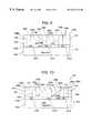
- an underlying gallium nitride layer 104is grown on a substrate 102 .
- the substrate 102includes a sapphire (Al 2 O 3 ) substrate 102 a , preferably with (0001) (c-plane) orientation, and also preferably includes an aluminum nitride and/or gallium nitride buffer layer 102 b .
- the crystallographic designation conventions used hereinare well known to those having skill in the art, and need not be described further.
- the gallium nitride layer 104may be between 0.5 and 2.0 ⁇ m thick, and may be grown at 1000° C. on a low temperature (600° C.) aluminum nitride buffer layer and/or a low temperature (500°) gallium nitride buffer layer 102 b that was deposited on the sapphire substrate 102 a in a cold wall vertical and inductively heated metalorganic vapor phase epitaxy system using triethylgallium at 26 ⁇ mol/min, ammonia at 1500 sccm and 3000 sccm hydrogen diluent.
- the underlying gallium nitride layer 104includes a plurality of sidewalls 105 therein.
- the sidewalls 105may be thought of as being defined by a plurality of spaced apart posts 106 , that also may be referred to as “mesas”, “pedestals” or “columns”.
- the sidewalls 105may also be thought of as being defined by a plurality of trenches 107 , also referred to as “wells” in the underlying gallium nitride layer 104 .
- the sidewalls 105may also be thought of as being defined by a series of alternating trenches 107 and posts 106 .
- a single post 106may be provided, that may be thought of as being defined by at least one trench 107 adjacent the single post.
- the posts 106 and the trenches 107 that define the sidewalls 105may be fabricated by selective etching and/or selective epitaxial growth and/or other conventional techniques.
- the sidewallsneed not be orthogonal to the substrate 102 , but rather may be oblique thereto.
- the posts 106 and trenches 107may define elongated regions that are straight, V-shaped or have other shapes.
- the trenches 107preferably extend into the buffer layer 102 b and into the substrate 102 a , so that subsequent gallium nitride growth occurs preferentially on the sidewalls 105 rather than on the trench floors.
- the sidewalls 105 of the underlying gallium nitride layer 104are laterally grown to form a lateral gallium nitride layer 108 a in the trenches 107 .
- Lateral growth of gallium nitridemay be obtained at 1000-1100° C. and 45 Torr.
- the precursors TEG at 13-39 ⁇ mol/min and NH 3 at 1500 sccmmay be used in combination with a 3000 sccm H 2 diluent. If gallium nitride alloys are formed, additional conventional precursors of aluminum or indium, for example, may also be used.
- the term “lateral”means a direction that is orthogonal to the sidewalls 105 . It will also be understood that some vertical growth on the posts 106 may also take place during the lateral growth from sidewalls 105 .
- the term “vertical”denotes a directional parallel to the sidewalls 105 .
- gallium nitridecan nucleate on the sapphire.
- vertical growth of gallium nitridemay take place from the sapphire trench floors, that can interfere with lateral growth of the gallium nitride sidewalls into the at least one trench.
- the exposed areas of the surface of the sapphiremay be converted to aluminum nitride.
- gallium nitridecan nucleate well on aluminum nitride, and thereby allow vertical growth of the gallium nitride from the trench floor, which can interfere with the lateral growth of the gallium nitride sidewalls.
- the conversion of the exposed areas of the surface of the sapphire to aluminum nitridemay be reduced and preferably eliminated by using a high growth temperature for growing the gallium nitride.
- a high growth temperature for growing the gallium nitrideFor example, a temperature of about 1100° C. may be used rather than a conventional temperature of about 1000° C. However, this still may not prevent the nucleation of gallium nitride on the floor of the sapphire substrate.
- the sapphire substrate 102 ais etched sufficiently deep to prevent vertical growth of gallium nitride from the sapphire trench floor 107 a from interfering with the step of laterally growing the gallium nitride sidewalls of the at least one post into the at least one trench.
- the ratio of the sapphire sidewall height y to the sapphire floor width xmay be at least 1/4. Other ratios may be used depending on the vertical to lateral growth rate ratio during gallium nitride growth. Under the conditions described below, the lateral growth rate of gallium nitride can be faster than the vertical growth rate.
- the sidewall growth from the postscan coalesce over the trenches before the vertical gallium nitride growth in the trenches that results from nucleation of gallium nitride on the sapphire substrate can interfere with the lateral growth.
- continued growth of the lateral gallium nitride layer 108 acauses vertical growth onto the underlying gallium nitride layer 104 , specifically onto the posts 106 , to form a vertical gallium nitride layer 108 b .
- Growth conditions for vertical growthmay be maintained as was described in connection with FIG. 2 .
- continued vertical growth into trenches 107may take place at the bottom of the trenches.
- a void 109preferably remains between the lateral gallium nitride layer 108 a and the trench floor 107 a.
- growthis allowed to continue until the lateral growth fronts coalesce in the trenches 107 at the interfaces 108 c , to form a continuous gallium nitride semiconductor layer in the trenches.
- the total growth timemay be approximately 60 minutes.
- microelectronic devices 110may then be formed in the lateral gallium nitride semiconductor layer 108 a .
- Devicesmay also be formed in vertical gallium nitride layer 108 b.
- gallium nitride semiconductor structures 100include the substrate 102 .
- the substrateincludes the sapphire substrate 102 a and the aluminum nitride buffer layer 102 b on the sapphire substrate 102 a .
- the aluminum nitride and/or gallium nitride buffer layer 102 bmay be about 200-300 ⁇ thick.
- the underlying gallium nitride layer 104is also included on the buffer layer 102 b opposite the substrate 102 a .
- the underlying gallium nitride layer 104may be between about 0.5 and 2.0 ⁇ m thick, and may be formed using metalorganic vapor phase epitaxy (MOVPE).
- MOVPEmetalorganic vapor phase epitaxy
- the underlying gallium nitride layergenerally has an undesired relatively high defect density. For example, dislocation densities of between about 10 8 and 10 10 cm ⁇ 2 may be present in the underlying gallium nitride layer. These high defect densities may result from mismatches in lattice parameters between the buffer layer 102 b and the underlying gallium nitride layer 104 , and/or other causes. These high defect densities may impact the performance of microelectronic devices formed in the underlying gallium nitride layer 104 .
- the underlying gallium nitride layer 104includes the plurality of sidewalls 105 that may be defined by the plurality of posts 106 and/or the plurality of trenches 107 .
- the sidewallsmay be oblique and of various elongated shapes.
- the posts 106include a gallium nitride top, a gallium nitride sidewall and a sapphire sidewall, and the at least one trench includes a sapphire floor 107 a .
- the sapphire floor 107 apreferably is free of a vertical gallium nitride layer thereon.
- the sapphire sidewall height to sapphire floor width ratiopreferably is at least 1/4.
- the lateral gallium nitride layer 108 aextends from the plurality of sidewalls 105 of the underlying gallium nitride layer 104 .
- the lateral gallium nitride layer 108 amay be formed using metalorganic vapor phase epitaxy at about 1000-1100° C. and 45 Torr. Precursors of triethygallium (TEG) at 13-39 ⁇ mol/min and ammonia (NH 3 ) at 1500 sccm may be used in combination with a 3000 sccm H 2 diluent, to form the lateral gallium nitride layer 108 a .
- the gallium nitride semiconductor structure 100also includes the vertical gallium nitride layer 108 b that extends vertically from the posts 106 .
- the lateral gallium nitride layer 108 acoalesces at the interfaces 108 c to form a continuous lateral gallium nitride semiconductor layer 108 a in the trenches. It has been found that the dislocation densities in the underlying gallium nitride layer 104 generally do not propagate laterally from the sidewalls 105 with the same density as vertically from the underlying gallium nitride layer 104 . Thus, the lateral gallium nitride layer 108 a can have a relatively low defect density, for example less that 10 4 cm ⁇ 2 . Accordingly, the lateral gallium nitride layer 108 b may form device quality gallium nitride semiconductor material.
- microelectronic devices 110may be formed in the lateral gallium nitride semiconductor layer 108 a . It will also be understood that a mask need not be used to fabricate the gallium nitride semiconductor structures 100 of FIG. 5, because lateral growth is directed from the sidewalls 105 .
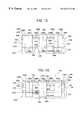
- FIGS. 6-10illustrate other embodiments according to the present invention.
- a mask 201is formed on the trench floors 107 a ′.
- the trenchneed not be etched into the sapphire substrate 102 a . Rather, as shown in FIG. 6, the trench may only be etched through the aluminum nitride buffer layer 102 b .
- the trenchalso may be etched into the sapphire substrate 102 a , as was illustrated in FIG. 1, and the trench floor 107 a in the sapphire substrate may be masked with a mask 201 .
- the trenchmay be etched only partially into the aluminum nitride buffer layer 102 b , rather than entirely through the aluminum nitride buffer layer 102 b as shown in FIG. 6 .
- the trenchneed not be etched into the aluminum nitride buffer layer 102 b at all, but rather the mask 201 may be formed on the exposed portion of the aluminum nitride buffer layer 102 b .
- the trenchesmay not extend into the aluminum nitride buffer layer, but rather may terminate within the gallium nitride layer 104 , and the mask 201 may be formed on the gallium nitride floor.
- the mask 201is shown to have the same thickness as the aluminum nitride buffer layer 102 b , it need not have the same thickness. Rather, it can be thinner or thicker.
- gallium nitridedoes not nucleate appreciably on certain amorphous and crystalline materials, such as silicon dioxide, silicon nitride and certain metals such as tungsten. Accordingly, a “line of sight” deposition technique, such as thermal evaporation or electron beam evaporation, may be used to deposit a masking material such as silicon dioxide, silicon nitride and/or tungsten on the trench floors. Since the gallium nitride does not nucleate specifically on the mask, it can be forced to grow off the sidewalls of the posts only. The remaining processing steps of FIGS. 6-10 correspond to those of FIGS. 1-5, and need not be described again herein.
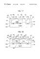
- FIGS. 11-16illustrate yet other embodiments according to the present invention.
- the sapphire substrate 102 ais etched sufficiently deep to prevent vertical growth of gallium nitride from the sapphire floor from interfering with the step of laterally growing the gallium nitride sidewalls of the at least one post into the at least one trench, as was described in connection with FIGS. 1-5, and need not be described herein again.
- a masksuch as a silicon dioxide, silicon nitride and/or tungsten mask 209 is included on the underlying gallium nitride layer 104 .
- the mask 209may have a thickness of about 1000 ⁇ or less and may be formed on the underlying gallium nitride layer 104 using low pressure Chemical Vapor Deposition (CVD) of silicon dioxide and/or silicon nitride. Alternatively, electron beam or thermal evaporation may be used to deposit tungsten.
- the mask 209is patterned to provide an array of openings therein, using conventional photolithography techniques.
- the underlying gallium nitride layeris etched through the array of openings to define the plurality of posts 106 in the underlying gallium nitride layer 104 and the plurality of trenches 107 therebetween.
- the postseach include the sidewall 105 and a top having the mask 209 thereon.
- the posts 106 and trenches 107are preferably formed by masking and etching as described above, the posts may also be formed by selectively growing the posts from an underlying gallium nitride layer and then forming a capping layer on the tops of the posts. Combinations of selective growth and selective etching also may be used.
- the sidewalls 105 of the underlying gallium nitride layer 104are laterally grown to form a lateral gallium nitride layer 108 a in the trenches 107 . Lateral growth may proceed as was described above. It will be understood that growth and/or nucleation on the top of the posts 106 is reduced and preferably eliminated by the mask 209 .
- lateral gallium nitride layer 108 acauses lateral overgrowth onto the mask 209 , to form an overgrown lateral gallium nitride layer 108 b .
- Growth conditions for overgrowthmay be maintained as was described in connection with FIG. 12 .
- growthis allowed to continue until the lateral growth fronts coalesce in the trenches 107 at the interfaces 108 c , to form a continuous lateral gallium nitride semiconductor layer 108 a in the trenches.
- growthis also allowed to continue until the lateral overgrowth fronts coalesce over the mask 209 at the interfaces 108 d , to form a continuous overgrown lateral gallium nitride semiconductor layer 108 b .
- the total growth timemay be approximately 60 minutes.
- a single continuous growth stepmay be used.
- microelectronic devices 110may then be formed in the lateral gallium nitride semiconductor layer 108 a .
- Microelectronic devicesalso may be formed in the overgrown lateral gallium nitride layer 108 b.
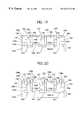
- FIGS. 17-22combine the mask 201 on the floor of the trenches 107 , as was illustrated in FIGS. 6-10, with the mask 209 on the top of the posts 106 , as was illustrated in FIG. 11 .
- the mask 201 at the bottom of the trenches, and the mask 209 on the top of the posts 106preferably are formed simultaneously and preferably comprise the same material. Accordingly, for example, line of sight of deposition techniques, such as thermal evaporation or electron beam evaporation of masking material such as silicon dioxide, silicon nitride and/or metal such as tungsten may be used.
- the mask materialis deposited after the etching step, it covers only the vertical surfaces, i.e. the top surfaces of the posts 106 and the bottom surfaces (floors) of the trenches 107 .
- the gallium nitridepreferably nucleates little, if at all, on the masks 201 and 209 , so that gallium nitride preferably only grows from the sidewalls 105 of the posts.
- the masks 201 and 209may comprise different materials and/or be of different thicknesses.
- the remaining steps of FIGS. 17-22are similar to FIGS. 11-16, and need not be described again in detail.
- the masks 201may be formed on an exposed sapphire floor of the substrate 102 a , on an exposed aluminum nitride floor of layer 102 b , or on an exposed gallium nitride floor in layer 104 .
- the trenchesmay be etched partly into gallium nitride layer 104 , fully through gallium nitride layer 104 , partly into aluminum nitride buffer layer 102 b , fully through aluminum nitride layer 102 b , and/or partly into sapphire substrate 102 a .
- the thickness of the mask 201may be thinner than or thicker than aluminum nitride layer 102 b . Accordingly, sapphire substrates may be used for growth of gallium nitride semiconductor layers, to thereby provide low cost and/or high availability.
Landscapes
- Engineering & Computer Science (AREA)
- Microelectronics & Electronic Packaging (AREA)
- Condensed Matter Physics & Semiconductors (AREA)
- General Physics & Mathematics (AREA)
- Manufacturing & Machinery (AREA)
- Computer Hardware Design (AREA)
- Physics & Mathematics (AREA)
- Power Engineering (AREA)
- Chemical & Material Sciences (AREA)
- Crystallography & Structural Chemistry (AREA)
- Materials Engineering (AREA)
- Led Devices (AREA)
- Recrystallisation Techniques (AREA)
- Crystals, And After-Treatments Of Crystals (AREA)
- Semiconductor Lasers (AREA)
Abstract
Description
Claims (35)
Priority Applications (16)
| Application Number | Priority Date | Filing Date | Title |
|---|---|---|---|
| US09/441,753US6521514B1 (en) | 1999-11-17 | 1999-11-17 | Pendeoepitaxial methods of fabricating gallium nitride semiconductor layers on sapphire substrates |
| CA002392041ACA2392041C (en) | 1999-11-17 | 2000-10-04 | Pendeoepitaxial growth of gallium nitride layers on sapphire substrates |
| KR1020027006379AKR100810192B1 (en) | 1999-11-17 | 2000-10-04 | Fender epitaxial growth of gallium nitride layer on sapphire substrate |
| EP00970569AEP1232520B1 (en) | 1999-11-17 | 2000-10-04 | Pendeoepitaxial growth of gallium nitride layers on sapphire substrates |
| AT00970569TATE537555T1 (en) | 1999-11-17 | 2000-10-04 | PENDEOEPITACTIC GROWTH OF GALLIUM NITRIDE LAYERS ON SAPPHIRE SUBSTRATES |
| EP10191674AEP2302665A1 (en) | 1999-11-17 | 2000-10-04 | Pendeoepitaxial growth of gallium nitride layers on sapphire substrates |
| AU79929/00AAU7992900A (en) | 1999-11-17 | 2000-10-04 | Pendeoepitaxial growth of gallium nitride layers on sapphire substrates |
| PCT/US2000/027354WO2001037327A1 (en) | 1999-11-17 | 2000-10-04 | Pendeoepitaxial growth of gallium nitride layers on sapphire substrates |
| JP2001537783AJP4017140B2 (en) | 1999-11-17 | 2000-10-04 | Method for manufacturing gallium nitride semiconductor layer |
| CNB008171823ACN100364051C (en) | 1999-11-17 | 2000-10-04 | Suspended Epitaxial Growth of Gallium Nitride Layers on Sapphire Substrates |
| US09/780,715US6489221B2 (en) | 1999-11-17 | 2001-02-09 | High temperature pendeoepitaxial methods of fabricating gallium nitride semiconductor layers on sapphire substrates |
| US09/899,586US6545300B2 (en) | 1999-11-17 | 2001-07-03 | Pendeoepitaxial methods of fabricating gallium nitride semiconductor layers on sapphire substrates, and gallium nitride semiconductor structures fabricated thereby |
| JP2002048444AJP4410972B2 (en) | 1999-11-17 | 2002-02-25 | Method for manufacturing gallium nitride semiconductor layer |
| JP2002048445AJP4223219B2 (en) | 1999-11-17 | 2002-02-25 | Method for manufacturing gallium nitride semiconductor layer |
| US10/404,616US6686261B2 (en) | 1999-11-17 | 2003-04-01 | Pendeoepitaxial methods of fabricating gallium nitride semiconductor layers on sapphire substrates, and gallium nitride semiconductor structures fabricated thereby |
| US10/763,588US7217641B2 (en) | 1999-11-17 | 2004-01-23 | Pendeoepitaxial methods of fabricating gallium nitride semiconductor layers on sapphire substrates, and gallium nitride semiconductor structures fabricated thereby |
Applications Claiming Priority (1)
| Application Number | Priority Date | Filing Date | Title |
|---|---|---|---|
| US09/441,753US6521514B1 (en) | 1999-11-17 | 1999-11-17 | Pendeoepitaxial methods of fabricating gallium nitride semiconductor layers on sapphire substrates |
Related Child Applications (2)
| Application Number | Title | Priority Date | Filing Date |
|---|---|---|---|
| US09/780,715ContinuationUS6489221B2 (en) | 1999-11-17 | 2001-02-09 | High temperature pendeoepitaxial methods of fabricating gallium nitride semiconductor layers on sapphire substrates |
| US09/899,586DivisionUS6545300B2 (en) | 1999-11-17 | 2001-07-03 | Pendeoepitaxial methods of fabricating gallium nitride semiconductor layers on sapphire substrates, and gallium nitride semiconductor structures fabricated thereby |
Publications (1)
| Publication Number | Publication Date |
|---|---|
| US6521514B1true US6521514B1 (en) | 2003-02-18 |
Family
ID=23754137
Family Applications (5)
| Application Number | Title | Priority Date | Filing Date |
|---|---|---|---|
| US09/441,753Expired - LifetimeUS6521514B1 (en) | 1999-11-17 | 1999-11-17 | Pendeoepitaxial methods of fabricating gallium nitride semiconductor layers on sapphire substrates |
| US09/780,715Expired - LifetimeUS6489221B2 (en) | 1999-11-17 | 2001-02-09 | High temperature pendeoepitaxial methods of fabricating gallium nitride semiconductor layers on sapphire substrates |
| US09/899,586Expired - LifetimeUS6545300B2 (en) | 1999-11-17 | 2001-07-03 | Pendeoepitaxial methods of fabricating gallium nitride semiconductor layers on sapphire substrates, and gallium nitride semiconductor structures fabricated thereby |
| US10/404,616Expired - LifetimeUS6686261B2 (en) | 1999-11-17 | 2003-04-01 | Pendeoepitaxial methods of fabricating gallium nitride semiconductor layers on sapphire substrates, and gallium nitride semiconductor structures fabricated thereby |
| US10/763,588Expired - LifetimeUS7217641B2 (en) | 1999-11-17 | 2004-01-23 | Pendeoepitaxial methods of fabricating gallium nitride semiconductor layers on sapphire substrates, and gallium nitride semiconductor structures fabricated thereby |
Family Applications After (4)
| Application Number | Title | Priority Date | Filing Date |
|---|---|---|---|
| US09/780,715Expired - LifetimeUS6489221B2 (en) | 1999-11-17 | 2001-02-09 | High temperature pendeoepitaxial methods of fabricating gallium nitride semiconductor layers on sapphire substrates |
| US09/899,586Expired - LifetimeUS6545300B2 (en) | 1999-11-17 | 2001-07-03 | Pendeoepitaxial methods of fabricating gallium nitride semiconductor layers on sapphire substrates, and gallium nitride semiconductor structures fabricated thereby |
| US10/404,616Expired - LifetimeUS6686261B2 (en) | 1999-11-17 | 2003-04-01 | Pendeoepitaxial methods of fabricating gallium nitride semiconductor layers on sapphire substrates, and gallium nitride semiconductor structures fabricated thereby |
| US10/763,588Expired - LifetimeUS7217641B2 (en) | 1999-11-17 | 2004-01-23 | Pendeoepitaxial methods of fabricating gallium nitride semiconductor layers on sapphire substrates, and gallium nitride semiconductor structures fabricated thereby |
Country Status (9)
| Country | Link |
|---|---|
| US (5) | US6521514B1 (en) |
| EP (2) | EP1232520B1 (en) |
| JP (3) | JP4017140B2 (en) |
| KR (1) | KR100810192B1 (en) |
| CN (1) | CN100364051C (en) |
| AT (1) | ATE537555T1 (en) |
| AU (1) | AU7992900A (en) |
| CA (1) | CA2392041C (en) |
| WO (1) | WO2001037327A1 (en) |
Cited By (93)
| Publication number | Priority date | Publication date | Assignee | Title |
|---|---|---|---|---|
| US20030162340A1 (en)* | 2000-03-14 | 2003-08-28 | Yuta Tezen | Group III nitride compound semiconductor and method for manufacturing the same |
| US20040119067A1 (en)* | 2000-12-14 | 2004-06-24 | Nitronex Corporation | Gallium nitride materials and methods |
| US6770914B2 (en)* | 2001-06-13 | 2004-08-03 | Ngk Insulators, Ltd. | III nitride semiconductor substrate for ELO |
| US20040152321A1 (en)* | 1999-11-17 | 2004-08-05 | Thomas Gehrke | Pendeoepitaxial methods of fabricating gallium nitride semiconductor layers on sapphire substrates, and gallium nitride semiconductor structures fabricated thereby |
| US20050009304A1 (en)* | 1998-06-10 | 2005-01-13 | Tsvetanka Zheleva | Methods of fabricating gallium nitride semiconductor layers by lateral growth into trenches |
| US20050093099A1 (en)* | 2000-03-31 | 2005-05-05 | Toyoda Gosei Co., Ltd. | Method for fabricating group III nitride compound semiconductors and group III nitride compound semiconductor devices |
| US20050127397A1 (en)* | 2001-02-23 | 2005-06-16 | Nitronex Corporation | Gallium nitride materials including thermally conductive regions |
| US20050133818A1 (en)* | 2003-12-17 | 2005-06-23 | Johnson Jerry W. | Gallium nitride material devices including an electrode-defining layer and methods of forming the same |
| US20050145851A1 (en)* | 2003-12-17 | 2005-07-07 | Nitronex Corporation | Gallium nitride material structures including isolation regions and methods |
| US20050167775A1 (en)* | 2003-08-05 | 2005-08-04 | Nitronex Corporation | Gallium nitride material transistors and methods associated with the same |
| US20050186764A1 (en)* | 2004-02-20 | 2005-08-25 | National Chiao Tung University | Method for lifting offGaN pseudomask epitaxy layerusing wafer bonding way |
| US20050258450A1 (en)* | 2004-05-20 | 2005-11-24 | Saxler Adam W | Semiconductor devices having a hybrid channel layer, current aperture transistors and methods of fabricating same |
| US20050285141A1 (en)* | 2004-06-28 | 2005-12-29 | Piner Edwin L | Gallium nitride materials and methods associated with the same |
| US20050285155A1 (en)* | 2004-06-28 | 2005-12-29 | Nitronex Corporation | Semiconductor device-based sensors and methods associated with the same |
| US20060006500A1 (en)* | 2004-07-07 | 2006-01-12 | Nitronex Corporation | III-nitride materials including low dislocation densities and methods associated with the same |
| US20060017064A1 (en)* | 2004-07-26 | 2006-01-26 | Saxler Adam W | Nitride-based transistors having laterally grown active region and methods of fabricating same |
| US20060108606A1 (en)* | 2004-11-23 | 2006-05-25 | Saxler Adam W | Cap layers and/or passivation layers for nitride-based transistors, transistor structures and methods of fabricating same |
| US20060118823A1 (en)* | 2004-12-06 | 2006-06-08 | Primit Parikh | Field effect transistors (FETs) having multi-watt output power at millimeter-wave frequencies |
| US20060118809A1 (en)* | 2004-12-06 | 2006-06-08 | Primit Parikh | High power density and/or linearity transistors |
| US20060131606A1 (en)* | 2004-12-18 | 2006-06-22 | Amberwave Systems Corporation | Lattice-mismatched semiconductor structures employing seed layers and related fabrication methods |
| US20060208280A1 (en)* | 2005-03-15 | 2006-09-21 | Smith Richard P | Group III nitride field effect transistors (FETS) capable of withstanding high temperature reverse bias test conditions |
| US20060214289A1 (en)* | 2004-10-28 | 2006-09-28 | Nitronex Corporation | Gallium nitride material-based monolithic microwave integrated circuits |
| US20060226413A1 (en)* | 2005-04-11 | 2006-10-12 | Saxler Adam W | Composite substrates of conductive and insulating or semi-insulating group III-nitrides for group III-nitride devices |
| US20060226412A1 (en)* | 2005-04-11 | 2006-10-12 | Saxler Adam W | Thick semi-insulating or insulating epitaxial gallium nitride layers and devices incorporating same |
| US20060244011A1 (en)* | 2005-04-29 | 2006-11-02 | Saxler Adam W | Binary group III-nitride based high electron mobility transistors and methods of fabricating same |
| US20060244010A1 (en)* | 2005-04-29 | 2006-11-02 | Saxler Adam W | Aluminum free group III-nitride based high electron mobility transistors and methods of fabricating same |
| US20060249748A1 (en)* | 2005-05-03 | 2006-11-09 | Nitronex Corporation | Gallium nitride material structures including substrates and methods associated with the same |
| US20060267043A1 (en)* | 2005-05-27 | 2006-11-30 | Emerson David T | Deep ultraviolet light emitting devices and methods of fabricating deep ultraviolet light emitting devices |
| US20060276043A1 (en)* | 2003-03-21 | 2006-12-07 | Johnson Mark A L | Method and systems for single- or multi-period edge definition lithography |
| US20060292719A1 (en)* | 2005-05-17 | 2006-12-28 | Amberwave Systems Corporation | Lattice-mismatched semiconductor structures with reduced dislocation defect densities and related methods for device fabrication |
| US20070004184A1 (en)* | 2005-06-29 | 2007-01-04 | Saxler Adam W | Low dislocation density group III nitride layers on silicon carbide substrates and methods of making the same |
| US20070018198A1 (en)* | 2005-07-20 | 2007-01-25 | Brandes George R | High electron mobility electronic device structures comprising native substrates and methods for making the same |
| US20070054465A1 (en)* | 2005-09-07 | 2007-03-08 | Amberwave Systems Corporation | Lattice-mismatched semiconductor structures on insulators |
| US20070054467A1 (en)* | 2005-09-07 | 2007-03-08 | Amberwave Systems Corporation | Methods for integrating lattice-mismatched semiconductor structure on insulators |
| US20070141823A1 (en)* | 2005-12-12 | 2007-06-21 | Kyma Technologies, Inc. | Inclusion-free uniform semi-insulating group III nitride substrates and methods for making same |
| US20070164315A1 (en)* | 2004-11-23 | 2007-07-19 | Cree, Inc. | Cap Layers Including Aluminum Nitride for Nitride-Based Transistors and Methods of Fabricating Same |
| US20070164322A1 (en)* | 2006-01-17 | 2007-07-19 | Cree, Inc. | Methods of fabricating transistors including dielectrically-supported gate electrodes and related devices |
| US7247889B2 (en) | 2004-12-03 | 2007-07-24 | Nitronex Corporation | III-nitride material structures including silicon substrates |
| US20070181977A1 (en)* | 2005-07-26 | 2007-08-09 | Amberwave Systems Corporation | Solutions for integrated circuit integration of alternative active area materials |
| US20070190755A1 (en)* | 2006-02-16 | 2007-08-16 | Samsung Electronics Co., Ltd. | Substrate for growing Pendeo epitaxy and method of forming the same |
| US20070202360A1 (en)* | 2005-10-04 | 2007-08-30 | Nitronex Corporation | Gallium nitride material transistors and methods for wideband applications |
| US20070267722A1 (en)* | 2006-05-17 | 2007-11-22 | Amberwave Systems Corporation | Lattice-mismatched semiconductor structures with reduced dislocation defect densities and related methods for device fabrication |
| US20070272957A1 (en)* | 2005-12-02 | 2007-11-29 | Nitronex Corporation | Gallium nitride material devices and associated methods |
| US20080001169A1 (en)* | 2006-03-24 | 2008-01-03 | Amberwave Systems Corporation | Lattice-mismatched semiconductor structures and related methods for device fabrication |
| US20080035143A1 (en)* | 2006-08-14 | 2008-02-14 | Sievers Robert E | Human-powered dry powder inhaler and dry powder inhaler compositions |
| US20080070355A1 (en)* | 2006-09-18 | 2008-03-20 | Amberwave Systems Corporation | Aspect ratio trapping for mixed signal applications |
| US20080073667A1 (en)* | 2006-09-27 | 2008-03-27 | Amberwave Systems Corporation | Tri-gate field-effect transistors formed by aspect ratio trapping |
| US20080073641A1 (en)* | 2006-09-27 | 2008-03-27 | Amberwave Systems Corporation | Quantum tunneling devices and circuits with lattice-mismatched semiconductor structures |
| US20080093622A1 (en)* | 2006-10-19 | 2008-04-24 | Amberwave Systems Corporation | Light-Emitter-Based Devices with Lattice-Mismatched Semiconductor Structures |
| US20080099785A1 (en)* | 2006-09-07 | 2008-05-01 | Amberwave Systems Coporation | Defect Reduction Using Aspect Ratio Trapping |
| US7378684B2 (en) | 1998-11-24 | 2008-05-27 | North Carolina State University | Pendeoepitaxial gallium nitride semiconductor layers on silicon carbide substrates |
| US20090042344A1 (en)* | 2007-06-15 | 2009-02-12 | Amberwave Systems Corporation | InP-Based Transistor Fabrication |
| US20090039361A1 (en)* | 2005-05-17 | 2009-02-12 | Amberwave Systems Corporation | Lattice-mismatched semiconductor structures with reduced dislocation defect densities and related methods for device fabrication |
| US20090065047A1 (en)* | 2007-09-07 | 2009-03-12 | Amberwave Systems Corporation | Multi-Junction Solar Cells |
| US20090079034A1 (en)* | 2007-09-26 | 2009-03-26 | Wang Nang Wang | Non-polar iii-v nitride semiconductor and growth method |
| US20090174038A1 (en)* | 2007-01-19 | 2009-07-09 | Wang Nang Wang | Production of single-crystal semiconductor material using a nanostructure template |
| US7566913B2 (en) | 2005-12-02 | 2009-07-28 | Nitronex Corporation | Gallium nitride material devices including conductive regions and methods associated with the same |
| US20090194773A1 (en)* | 2008-02-05 | 2009-08-06 | Nitronex Corporation | Gallium nitride material devices including diamond regions and methods associated with the same |
| US20090224289A1 (en)* | 2006-01-17 | 2009-09-10 | Cree, Inc. | Transistors including supported gate electrodes |
| US20090243043A1 (en)* | 2006-03-23 | 2009-10-01 | Wang Nang Wang | Growth method using nanostructure compliant layers and hvpe for producing high quality compound semiconductor materials |
| US20090267188A1 (en)* | 2008-04-29 | 2009-10-29 | Nitronex Corporation | Gallium nitride material processing and related device structures |
| US20100072515A1 (en)* | 2008-09-19 | 2010-03-25 | Amberwave Systems Corporation | Fabrication and structures of crystalline material |
| US20100078680A1 (en)* | 2008-09-24 | 2010-04-01 | Amberwave Systems Corporation | Semiconductor sensor structures with reduced dislocation defect densities and related methods for the same |
| US7745848B1 (en) | 2007-08-15 | 2010-06-29 | Nitronex Corporation | Gallium nitride material devices and thermal designs thereof |
| US20100176371A1 (en)* | 2009-01-09 | 2010-07-15 | Taiwan Semiconductor Manufacturing Company, Ltd. | Semiconductor Diodes Fabricated by Aspect Ratio Trapping with Coalesced Films |
| US20100176375A1 (en)* | 2009-01-09 | 2010-07-15 | Taiwan Semiconductor Manufacturing Company, Ltd. | Diode-Based Devices and Methods for Making the Same |
| US20100252861A1 (en)* | 2009-04-02 | 2010-10-07 | Taiwan Semiconductor Manufacturing Company, Ltd. | Devices Formed from a Non-Polar Plane of a Crystalline Material and Method of Making the Same |
| US20110011438A1 (en)* | 2007-04-09 | 2011-01-20 | Taiwan Semiconductor Manufacturing Company, Ltd. | Nitride-Based Multi-Junction Solar Cell Modules and Methods for Making the Same |
| US20110049568A1 (en)* | 2005-05-17 | 2011-03-03 | Taiwan Semiconductor Manufacturing Company, Ltd. | Lattice-Mismatched Semiconductor Structures with Reduced Dislocation Defect Densities and Related Methods for Device Fabrication |
| US8183627B2 (en) | 2004-12-01 | 2012-05-22 | Taiwan Semiconductor Manufacturing Company, Ltd. | Hybrid fin field-effect transistor structures and related methods |
| US8274097B2 (en) | 2008-07-01 | 2012-09-25 | Taiwan Semiconductor Manufacturing Company, Ltd. | Reduction of edge effects from aspect ratio trapping |
| US8384196B2 (en) | 2008-09-19 | 2013-02-26 | Taiwan Semiconductor Manufacturing Company, Ltd. | Formation of devices by epitaxial layer overgrowth |
| US8822248B2 (en) | 2008-06-03 | 2014-09-02 | Taiwan Semiconductor Manufacturing Company, Ltd. | Epitaxial growth of crystalline material |
| US20150053916A1 (en)* | 2013-08-22 | 2015-02-26 | Nanoco Technologies Ltd. | Gas Phase Enhancement of Emission Color Quality in Solid State LEDs |
| US8981427B2 (en) | 2008-07-15 | 2015-03-17 | Taiwan Semiconductor Manufacturing Company, Ltd. | Polishing of small composite semiconductor materials |
| US20150194442A1 (en)* | 2012-10-12 | 2015-07-09 | Sumitomo Electric Industries, Ltd | Group iii nitride composite substrate and method for manufacturing the same, and method for manufacturing group iii nitride semiconductor device |
| US9508890B2 (en) | 2007-04-09 | 2016-11-29 | Taiwan Semiconductor Manufacturing Company, Ltd. | Photovoltaics on silicon |
| US9627473B2 (en) | 2015-09-08 | 2017-04-18 | Macom Technology Solutions Holdings, Inc. | Parasitic channel mitigation in III-nitride material semiconductor structures |
| US9673281B2 (en) | 2015-09-08 | 2017-06-06 | Macom Technology Solutions Holdings, Inc. | Parasitic channel mitigation using rare-earth oxide and/or rare-earth nitride diffusion barrier regions |
| US9704705B2 (en) | 2015-09-08 | 2017-07-11 | Macom Technology Solutions Holdings, Inc. | Parasitic channel mitigation via reaction with active species |
| US9773898B2 (en) | 2015-09-08 | 2017-09-26 | Macom Technology Solutions Holdings, Inc. | III-nitride semiconductor structures comprising spatially patterned implanted species |
| US9799520B2 (en) | 2015-09-08 | 2017-10-24 | Macom Technology Solutions Holdings, Inc. | Parasitic channel mitigation via back side implantation |
| US9806182B2 (en) | 2015-09-08 | 2017-10-31 | Macom Technology Solutions Holdings, Inc. | Parasitic channel mitigation using elemental diboride diffusion barrier regions |
| US9923063B2 (en) | 2013-02-18 | 2018-03-20 | Sumitomo Electric Industries, Ltd. | Group III nitride composite substrate and method for manufacturing the same, laminated group III nitride composite substrate, and group III nitride semiconductor device and method for manufacturing the same |
| US10186451B2 (en) | 2013-02-08 | 2019-01-22 | Sumitomo Electric Industries, Ltd. | Group III nitride composite substrate and method for manufacturing the same, and method for manufacturing group III nitride semiconductor device |
| US10211294B2 (en) | 2015-09-08 | 2019-02-19 | Macom Technology Solutions Holdings, Inc. | III-nitride semiconductor structures comprising low atomic mass species |
| US10756183B2 (en) | 2014-12-18 | 2020-08-25 | Intel Corporation | N-channel gallium nitride transistors |
| US10930500B2 (en) | 2014-09-18 | 2021-02-23 | Intel Corporation | Wurtzite heteroepitaxial structures with inclined sidewall facets for defect propagation control in silicon CMOS-compatible semiconductor devices |
| US11038023B2 (en) | 2018-07-19 | 2021-06-15 | Macom Technology Solutions Holdings, Inc. | III-nitride material semiconductor structures on conductive silicon substrates |
| US11177376B2 (en) | 2014-09-25 | 2021-11-16 | Intel Corporation | III-N epitaxial device structures on free standing silicon mesas |
| US11233053B2 (en) | 2017-09-29 | 2022-01-25 | Intel Corporation | Group III-nitride (III-N) devices with reduced contact resistance and their methods of fabrication |
| US11264465B2 (en) | 2015-09-08 | 2022-03-01 | Macom Technology Solutions Holdings, Inc. | Parasitic channel mitigation using silicon carbide diffusion barrier regions |
| US12125888B2 (en) | 2017-09-29 | 2024-10-22 | Intel Corporation | Group III-nitride (III-N) devices with reduced contact resistance and their methods of fabrication |
Families Citing this family (66)
| Publication number | Priority date | Publication date | Assignee | Title |
|---|---|---|---|---|
| EP2234142A1 (en)* | 1997-04-11 | 2010-09-29 | Nichia Corporation | Nitride semiconductor substrate |
| US6403451B1 (en)* | 2000-02-09 | 2002-06-11 | Noerh Carolina State University | Methods of fabricating gallium nitride semiconductor layers on substrates including non-gallium nitride posts |
| JP5095064B2 (en) | 2000-08-04 | 2012-12-12 | ザ リージェンツ オブ ザ ユニバーシティ オブ カリフォルニア | Semiconductor film having nitride layer deposited on silicon substrate and method for manufacturing the same |
| US7619261B2 (en)* | 2000-08-07 | 2009-11-17 | Toyoda Gosei Co., Ltd. | Method for manufacturing gallium nitride compound semiconductor |
| US7233028B2 (en) | 2001-02-23 | 2007-06-19 | Nitronex Corporation | Gallium nitride material devices and methods of forming the same |
| US6611002B2 (en) | 2001-02-23 | 2003-08-26 | Nitronex Corporation | Gallium nitride material devices and methods including backside vias |
| JP3679720B2 (en)* | 2001-02-27 | 2005-08-03 | 三洋電機株式会社 | Nitride semiconductor device and method for forming nitride semiconductor |
| US20030132433A1 (en)* | 2002-01-15 | 2003-07-17 | Piner Edwin L. | Semiconductor structures including a gallium nitride material component and a silicon germanium component |
| JP3912117B2 (en)* | 2002-01-17 | 2007-05-09 | ソニー株式会社 | Crystal growth method, semiconductor light emitting device and method for manufacturing the same |
| JP4092927B2 (en)* | 2002-02-28 | 2008-05-28 | 豊田合成株式会社 | Group III nitride compound semiconductor, group III nitride compound semiconductor element, and method for manufacturing group III nitride compound semiconductor substrate |
| US7101433B2 (en)* | 2002-12-18 | 2006-09-05 | General Electric Company | High pressure/high temperature apparatus with improved temperature control for crystal growth |
| TWI255052B (en)* | 2003-02-14 | 2006-05-11 | Osram Opto Semiconductors Gmbh | Method to produce a number of semiconductor-bodies and electronic semiconductor-bodies |
| US7122827B2 (en) | 2003-10-15 | 2006-10-17 | General Electric Company | Monolithic light emitting devices based on wide bandgap semiconductor nanostructures and methods for making same |
| KR100512580B1 (en)* | 2003-12-31 | 2005-09-06 | 엘지전자 주식회사 | Method of growing nitride semiconductor thin film having small defects |
| KR20050077902A (en)* | 2004-01-29 | 2005-08-04 | 엘지전자 주식회사 | Method of growing nitride semiconductor thin film |
| KR101094403B1 (en)* | 2004-01-29 | 2011-12-15 | 삼성코닝정밀소재 주식회사 | Reduced warpage of sapphire / gallium nitride laminates |
| KR20070009370A (en) | 2004-05-06 | 2007-01-18 | 아사히 가라스 가부시키가이샤 | Laminated Dielectric Manufacturing Method |
| KR100674829B1 (en)* | 2004-10-29 | 2007-01-25 | 삼성전기주식회사 | Nitride-based semiconductor device and its manufacturing method |
| CN1300387C (en)* | 2004-11-12 | 2007-02-14 | 南京大学 | Process for non-mask transverse epitaxial growth of high quality gallium nitride |
| JP4604241B2 (en)* | 2004-11-18 | 2011-01-05 | 独立行政法人産業技術総合研究所 | Silicon carbide MOS field effect transistor and manufacturing method thereof |
| KR100682881B1 (en)* | 2005-01-19 | 2007-02-15 | 삼성코닝 주식회사 | Crystal growth method |
| JP4818732B2 (en)* | 2005-03-18 | 2011-11-16 | シャープ株式会社 | Method of manufacturing nitride semiconductor device |
| TW200703463A (en) | 2005-05-31 | 2007-01-16 | Univ California | Defect reduction of non-polar and semi-polar III-nitrides with sidewall lateral epitaxial overgrowth (SLEO) |
| US8168000B2 (en)* | 2005-06-15 | 2012-05-01 | International Rectifier Corporation | III-nitride semiconductor device fabrication |
| TWI304278B (en)* | 2006-06-16 | 2008-12-11 | Ind Tech Res Inst | Semiconductor emitting device substrate and method of fabricating the same |
| TW200805452A (en)* | 2006-07-06 | 2008-01-16 | Nat Univ Chung Hsing | Method of making a low-defect-density epitaxial substrate and the product made therefrom |
| JP5155536B2 (en)* | 2006-07-28 | 2013-03-06 | 一般財団法人電力中央研究所 | Method for improving the quality of SiC crystal and method for manufacturing SiC semiconductor device |
| WO2008115473A2 (en)* | 2007-03-15 | 2008-09-25 | The University Of Akron | Self-acting self-circulating fluid system without external pressure source and use in bearing system |
| KR20100020936A (en)* | 2007-07-12 | 2010-02-23 | 라티스 파워(지앙시) 코포레이션 | Method for obtaining high-quality boundary for semiconductor devices fabricated on a partitioned substrate |
| KR101226077B1 (en)* | 2007-11-27 | 2013-01-24 | 삼성전자주식회사 | Method of forming a sidewall spacer and method of manufacturing a semiconductor device using the same |
| JP5353113B2 (en)* | 2008-01-29 | 2013-11-27 | 豊田合成株式会社 | Method for producing group III nitride compound semiconductor |
| JP4247413B1 (en)* | 2008-03-19 | 2009-04-02 | 株式会社 東北テクノアーチ | Device manufacturing method |
| US9250249B2 (en) | 2008-09-08 | 2016-02-02 | Enzo Biochem, Inc. | Autophagy and phospholipidosis pathway assays |
| FR2936904B1 (en)* | 2008-10-03 | 2011-01-14 | Soitec Silicon On Insulator | METHODS AND STRUCTURES FOR ALTERING STRESS IN NITRIDE III MATERIALS. |
| US8367520B2 (en)* | 2008-09-22 | 2013-02-05 | Soitec | Methods and structures for altering strain in III-nitride materials |
| US8680581B2 (en)* | 2008-12-26 | 2014-03-25 | Toyoda Gosei Co., Ltd. | Method for producing group III nitride semiconductor and template substrate |
| US8313967B1 (en)* | 2009-01-21 | 2012-11-20 | Stc.Unm | Cubic phase, nitrogen-based compound semiconductor films epitaxially grown on a grooved Si <001> substrate |
| KR101640830B1 (en)* | 2009-08-17 | 2016-07-22 | 삼성전자주식회사 | Substrate structure and manufacturing method of the same |
| JP5685379B2 (en)* | 2010-01-28 | 2015-03-18 | 株式会社豊田中央研究所 | Manufacturing method of nitride semiconductor device |
| CN101820041A (en)* | 2010-04-01 | 2010-09-01 | 晶能光电(江西)有限公司 | Method and structure for reducing epitaxial stress of silicon substrate LED |
| TWI562195B (en)* | 2010-04-27 | 2016-12-11 | Pilegrowth Tech S R L | Dislocation and stress management by mask-less processes using substrate patterning and methods for device fabrication |
| SG185547A1 (en) | 2010-05-18 | 2012-12-28 | Agency Science Tech & Res | Method of forming a light emitting diode structure and a light emitting diode structure |
| EP2416350A1 (en)* | 2010-08-06 | 2012-02-08 | Imec | A method for selective deposition of a semiconductor material |
| US8592292B2 (en)* | 2010-09-02 | 2013-11-26 | National Semiconductor Corporation | Growth of multi-layer group III-nitride buffers on large-area silicon substrates and other substrates |
| KR20120082715A (en)* | 2011-01-14 | 2012-07-24 | 삼성엘이디 주식회사 | Semiconductor light emitting device and manufacturing method thereof |
| US10052848B2 (en) | 2012-03-06 | 2018-08-21 | Apple Inc. | Sapphire laminates |
| US9221289B2 (en) | 2012-07-27 | 2015-12-29 | Apple Inc. | Sapphire window |
| JP5731455B2 (en)* | 2012-09-07 | 2015-06-10 | 日本電信電話株式会社 | Optical modulator and manufacturing method thereof |
| US9232672B2 (en) | 2013-01-10 | 2016-01-05 | Apple Inc. | Ceramic insert control mechanism |
| JP5928366B2 (en)* | 2013-02-13 | 2016-06-01 | 豊田合成株式会社 | Method for producing group III nitride semiconductor |
| US9768271B2 (en)* | 2013-02-22 | 2017-09-19 | Micron Technology, Inc. | Methods, devices, and systems related to forming semiconductor power devices with a handle substrate |
| US9678540B2 (en) | 2013-09-23 | 2017-06-13 | Apple Inc. | Electronic component embedded in ceramic material |
| US9632537B2 (en) | 2013-09-23 | 2017-04-25 | Apple Inc. | Electronic component embedded in ceramic material |
| US9154678B2 (en) | 2013-12-11 | 2015-10-06 | Apple Inc. | Cover glass arrangement for an electronic device |
| US9225056B2 (en) | 2014-02-12 | 2015-12-29 | Apple Inc. | Antenna on sapphire structure |
| JP2015065465A (en)* | 2014-12-04 | 2015-04-09 | ▲さん▼圓光電股▲ふん▼有限公司 | Method of manufacturing light-emitting diode device |
| JP2016174054A (en)* | 2015-03-16 | 2016-09-29 | 株式会社東芝 | Semiconductor device and manufacturing method thereof |
| US9337022B1 (en)* | 2015-06-17 | 2016-05-10 | Globalfoundries Inc. | Virtual relaxed substrate on edge-relaxed composite semiconductor pillars |
| US10406634B2 (en) | 2015-07-01 | 2019-09-10 | Apple Inc. | Enhancing strength in laser cutting of ceramic components |
| US10087547B2 (en)* | 2015-12-21 | 2018-10-02 | The Regents Of The University Of California | Growth of single crystal III-V semiconductors on amorphous substrates |
| US9960127B2 (en) | 2016-05-18 | 2018-05-01 | Macom Technology Solutions Holdings, Inc. | High-power amplifier package |
| US10134658B2 (en) | 2016-08-10 | 2018-11-20 | Macom Technology Solutions Holdings, Inc. | High power transistors |
| CN110190163B (en)* | 2019-05-24 | 2020-04-28 | 康佳集团股份有限公司 | Patterned substrate, epitaxial wafer, manufacturing method, storage medium and LED chip |
| US10847625B1 (en)* | 2019-11-19 | 2020-11-24 | Opnovix Corp. | Indium-gallium-nitride structures and devices |
| US20240194822A1 (en)* | 2021-07-13 | 2024-06-13 | The Regents Of The University Of California | Fabrication method for small size light emiting diodes on high-quality epitaxial crystal layers |
| WO2024145658A1 (en) | 2022-12-30 | 2024-07-04 | Opnovix Corp. | Variable composition ternary compound semiconductor alloys, structures, and devices |
Citations (49)
| Publication number | Priority date | Publication date | Assignee | Title |
|---|---|---|---|---|
| US4127792A (en) | 1976-06-01 | 1978-11-28 | Mitsubishi Denki Kabushiki Kaisha | Luminescent semiconductor display device including gate control electrodes |
| US4522661A (en) | 1983-06-24 | 1985-06-11 | The United States Of America As Represented By The Administrator Of The National Aeronautics And Space Administration | Low defect, high purity crystalline layers grown by selective deposition |
| US4651407A (en) | 1985-05-08 | 1987-03-24 | Gte Laboratories Incorporated | Method of fabricating a junction field effect transistor utilizing epitaxial overgrowth and vertical junction formation |
| US4865685A (en) | 1987-11-03 | 1989-09-12 | North Carolina State University | Dry etching of silicon carbide |
| US4876210A (en) | 1987-04-30 | 1989-10-24 | The University Of Delaware | Solution growth of lattice mismatched and solubility mismatched heterostructures |
| US4912064A (en) | 1987-10-26 | 1990-03-27 | North Carolina State University | Homoepitaxial growth of alpha-SiC thin films and semiconductor devices fabricated thereon |
| US4946547A (en) | 1989-10-13 | 1990-08-07 | Cree Research, Inc. | Method of preparing silicon carbide surfaces for crystal growth |
| US4985742A (en)* | 1989-07-07 | 1991-01-15 | University Of Colorado Foundation, Inc. | High temperature semiconductor devices having at least one gallium nitride layer |
| JPH03132016A (en) | 1989-10-18 | 1991-06-05 | Canon Inc | Method of forming crystal |
| US5122845A (en) | 1989-03-01 | 1992-06-16 | Toyoda Gosei Co., Ltd. | Substrate for growing gallium nitride compound-semiconductor device and light emitting diode |
| JPH04188678A (en) | 1990-11-19 | 1992-07-07 | Matsushita Electric Ind Co Ltd | Semiconductor light-emitting element |
| US5156995A (en) | 1988-04-01 | 1992-10-20 | Cornell Research Foundation, Inc. | Method for reducing or eliminating interface defects in mismatched semiconductor epilayers |
| JPH057016A (en) | 1991-02-14 | 1993-01-14 | Toshiba Corp | Semiconductor light emitting device and manufacturing method thereof |
| JPH0541536A (en) | 1991-05-30 | 1993-02-19 | Kyocera Corp | Manufacture of semiconductor light emitting device |
| EP0551721A2 (en) | 1991-12-18 | 1993-07-21 | Amano, Hiroshi | Gallium nitride base semiconductor device and method of fabricating the same |
| USRE34861E (en) | 1987-10-26 | 1995-02-14 | North Carolina State University | Sublimation of silicon carbide to produce large, device quality single crystals of silicon carbide |
| US5397736A (en) | 1986-02-11 | 1995-03-14 | Max-Planck-Gesellschaft Zur Foerderung Der Wissenschaften | Liquid epitaxial process for producing three-dimensional semiconductor structures |
| JPH0818159A (en) | 1994-04-25 | 1996-01-19 | Hitachi Ltd | Semiconductor laser device and manufacturing method thereof |
| JPH0864791A (en) | 1994-08-23 | 1996-03-08 | Matsushita Electric Ind Co Ltd | Epitaxial growth method |
| JPH08116093A (en) | 1994-10-17 | 1996-05-07 | Fujitsu Ltd | Optical semiconductor device |
| JPH08125251A (en) | 1994-10-21 | 1996-05-17 | Matsushita Electric Ind Co Ltd | Hexagonal semiconductor ring resonator |
| JPH08153931A (en) | 1994-11-30 | 1996-06-11 | Nichia Chem Ind Ltd | Method for manufacturing gallium nitride-based compound semiconductor laser device |
| US5549747A (en) | 1980-04-10 | 1996-08-27 | Massachusetts Institute Of Technology | Method of producing sheets of crystalline material and devices made therefrom |
| WO1997011518A1 (en) | 1995-09-18 | 1997-03-27 | Hitachi, Ltd. | Semiconductor material, method of producing the semiconductor material, and semiconductor device |
| JPH0993315A (en) | 1995-09-20 | 1997-04-04 | Iwatsu Electric Co Ltd | Communication equipment structure |
| JPH09174494A (en) | 1995-12-21 | 1997-07-08 | Toyox Co Ltd | Square drilling machine for roof material |
| JPH09181071A (en) | 1995-12-16 | 1997-07-11 | Hyundai Electron Ind Co Ltd | Surface flattening method for bpsg films |
| JPH09201477A (en) | 1996-01-26 | 1997-08-05 | Kazuo Yui | Rocking mascot doll to be enclosed in transparent bottle and ornament using such doll |
| JPH09277448A (en) | 1996-04-15 | 1997-10-28 | Fujikura Ltd | How to connect plastic laminated paper |
| JPH09290098A (en) | 1996-04-26 | 1997-11-11 | Sanyo Electric Co Ltd | Clothes dryer |
| JPH09324997A (en) | 1996-06-05 | 1997-12-16 | Toshiba Corp | Heat exchanger and method for manufacturing heat exchanger |
| US5710057A (en) | 1996-07-12 | 1998-01-20 | Kenney; Donald M. | SOI fabrication method |
| US5760426A (en) | 1995-12-11 | 1998-06-02 | Mitsubishi Denki Kabushiki Kaisha | Heteroepitaxial semiconductor device including silicon substrate, GaAs layer and GaN layer #13 |
| US5786606A (en) | 1995-12-15 | 1998-07-28 | Kabushiki Kaisha Toshiba | Semiconductor light-emitting device |
| US5815520A (en) | 1995-07-27 | 1998-09-29 | Nec Corporation | light emitting semiconductor device and its manufacturing method |
| WO1998047170A1 (en) | 1997-04-11 | 1998-10-22 | Nichia Chemical Industries, Ltd. | Method of growing nitride semiconductors, nitride semiconductor substrate and nitride semiconductor device |
| US5877070A (en) | 1997-05-31 | 1999-03-02 | Max-Planck Society | Method for the transfer of thin layers of monocrystalline material to a desirable substrate |
| US5880485A (en) | 1997-03-24 | 1999-03-09 | Mitsubishi Denki Kabushiki Kaisha | Semiconductor device including Gallium nitride layer |
| JPH11145516A (en) | 1997-11-07 | 1999-05-28 | Toyoda Gosei Co Ltd | Manufacture of gallium nitride compound semiconductor |
| US5912477A (en) | 1994-10-07 | 1999-06-15 | Cree Research, Inc. | High efficiency light emitting diodes |
| US5915194A (en) | 1997-07-03 | 1999-06-22 | The United States Of America As Represented By The Administrator Of National Aeronautics And Space Administration | Method for growth of crystal surfaces and growth of heteroepitaxial single crystal films thereon |
| EP0951055A2 (en) | 1998-04-17 | 1999-10-20 | Hewlett-Packard Company | Epitaxial material grown laterally within a trench |
| US6051849A (en) | 1998-02-27 | 2000-04-18 | North Carolina State University | Gallium nitride semiconductor structures including a lateral gallium nitride layer that extends from an underlying gallium nitride layer |
| US6100111A (en) | 1998-03-23 | 2000-08-08 | Abb Research Ltd. | Method for fabricating a silicon carbide device |
| US6100104A (en) | 1997-09-19 | 2000-08-08 | Siemens Aktiengesellschaft | Method for fabricating a plurality of semiconductor bodies |
| US6156584A (en) | 1997-03-28 | 2000-12-05 | Rohm Co., Ltd. | Method of manufacturing a semiconductor light emitting device |
| US6177688B1 (en)* | 1998-11-24 | 2001-01-23 | North Carolina State University | Pendeoepitaxial gallium nitride semiconductor layers on silcon carbide substrates |
| JP3132016B2 (en) | 1991-01-11 | 2001-02-05 | 信越化学工業株式会社 | Method for producing high-purity chlorosilane |
| US6261929B1 (en)* | 2000-02-24 | 2001-07-17 | North Carolina State University | Methods of forming a plurality of semiconductor layers using spaced trench arrays |
Family Cites Families (6)
| Publication number | Priority date | Publication date | Assignee | Title |
|---|---|---|---|---|
| US5795798A (en)* | 1996-11-27 | 1998-08-18 | The Regents Of The University Of California | Method of making full color monolithic gan based leds |
| FR2769924B1 (en)* | 1997-10-20 | 2000-03-10 | Centre Nat Rech Scient | PROCESS FOR MAKING AN EPITAXIAL LAYER OF GALLIUM NITRIDE, EPITAXIAL LAYER OF GALLIUM NITRIDE AND OPTOELECTRONIC COMPONENT PROVIDED WITH SUCH A LAYER |
| US6064078A (en)* | 1998-05-22 | 2000-05-16 | Xerox Corporation | Formation of group III-V nitride films on sapphire substrates with reduced dislocation densities |
| US6265289B1 (en)* | 1998-06-10 | 2001-07-24 | North Carolina State University | Methods of fabricating gallium nitride semiconductor layers by lateral growth from sidewalls into trenches, and gallium nitride semiconductor structures fabricated thereby |
| US6335546B1 (en)* | 1998-07-31 | 2002-01-01 | Sharp Kabushiki Kaisha | Nitride semiconductor structure, method for producing a nitride semiconductor structure, and light emitting device |
| US6521514B1 (en)* | 1999-11-17 | 2003-02-18 | North Carolina State University | Pendeoepitaxial methods of fabricating gallium nitride semiconductor layers on sapphire substrates |
- 1999
- 1999-11-17USUS09/441,753patent/US6521514B1/ennot_activeExpired - Lifetime
- 2000
- 2000-10-04AUAU79929/00Apatent/AU7992900A/ennot_activeAbandoned
- 2000-10-04CACA002392041Apatent/CA2392041C/ennot_activeExpired - Fee Related
- 2000-10-04WOPCT/US2000/027354patent/WO2001037327A1/enactiveApplication Filing
- 2000-10-04EPEP00970569Apatent/EP1232520B1/ennot_activeExpired - Lifetime
- 2000-10-04JPJP2001537783Apatent/JP4017140B2/ennot_activeExpired - Lifetime
- 2000-10-04KRKR1020027006379Apatent/KR100810192B1/ennot_activeExpired - Fee Related
- 2000-10-04EPEP10191674Apatent/EP2302665A1/ennot_activeWithdrawn
- 2000-10-04CNCNB008171823Apatent/CN100364051C/ennot_activeExpired - Fee Related
- 2000-10-04ATAT00970569Tpatent/ATE537555T1/enactive
- 2001
- 2001-02-09USUS09/780,715patent/US6489221B2/ennot_activeExpired - Lifetime
- 2001-07-03USUS09/899,586patent/US6545300B2/ennot_activeExpired - Lifetime
- 2002
- 2002-02-25JPJP2002048444Apatent/JP4410972B2/ennot_activeExpired - Fee Related
- 2002-02-25JPJP2002048445Apatent/JP4223219B2/ennot_activeExpired - Fee Related
- 2003
- 2003-04-01USUS10/404,616patent/US6686261B2/ennot_activeExpired - Lifetime
- 2004
- 2004-01-23USUS10/763,588patent/US7217641B2/ennot_activeExpired - Lifetime
Patent Citations (55)
| Publication number | Priority date | Publication date | Assignee | Title |
|---|---|---|---|---|
| US4127792A (en) | 1976-06-01 | 1978-11-28 | Mitsubishi Denki Kabushiki Kaisha | Luminescent semiconductor display device including gate control electrodes |
| US5549747A (en) | 1980-04-10 | 1996-08-27 | Massachusetts Institute Of Technology | Method of producing sheets of crystalline material and devices made therefrom |
| US4522661A (en) | 1983-06-24 | 1985-06-11 | The United States Of America As Represented By The Administrator Of The National Aeronautics And Space Administration | Low defect, high purity crystalline layers grown by selective deposition |
| US4651407A (en) | 1985-05-08 | 1987-03-24 | Gte Laboratories Incorporated | Method of fabricating a junction field effect transistor utilizing epitaxial overgrowth and vertical junction formation |
| US5397736A (en) | 1986-02-11 | 1995-03-14 | Max-Planck-Gesellschaft Zur Foerderung Der Wissenschaften | Liquid epitaxial process for producing three-dimensional semiconductor structures |
| US4876210A (en) | 1987-04-30 | 1989-10-24 | The University Of Delaware | Solution growth of lattice mismatched and solubility mismatched heterostructures |
| US4912064A (en) | 1987-10-26 | 1990-03-27 | North Carolina State University | Homoepitaxial growth of alpha-SiC thin films and semiconductor devices fabricated thereon |
| USRE34861E (en) | 1987-10-26 | 1995-02-14 | North Carolina State University | Sublimation of silicon carbide to produce large, device quality single crystals of silicon carbide |
| US4865685A (en) | 1987-11-03 | 1989-09-12 | North Carolina State University | Dry etching of silicon carbide |
| US5156995A (en) | 1988-04-01 | 1992-10-20 | Cornell Research Foundation, Inc. | Method for reducing or eliminating interface defects in mismatched semiconductor epilayers |
| US5122845A (en) | 1989-03-01 | 1992-06-16 | Toyoda Gosei Co., Ltd. | Substrate for growing gallium nitride compound-semiconductor device and light emitting diode |
| US4985742A (en)* | 1989-07-07 | 1991-01-15 | University Of Colorado Foundation, Inc. | High temperature semiconductor devices having at least one gallium nitride layer |
| US4946547A (en) | 1989-10-13 | 1990-08-07 | Cree Research, Inc. | Method of preparing silicon carbide surfaces for crystal growth |
| JPH03132016A (en) | 1989-10-18 | 1991-06-05 | Canon Inc | Method of forming crystal |
| JPH04188678A (en) | 1990-11-19 | 1992-07-07 | Matsushita Electric Ind Co Ltd | Semiconductor light-emitting element |
| JP3132016B2 (en) | 1991-01-11 | 2001-02-05 | 信越化学工業株式会社 | Method for producing high-purity chlorosilane |
| JPH057016A (en) | 1991-02-14 | 1993-01-14 | Toshiba Corp | Semiconductor light emitting device and manufacturing method thereof |
| JPH0541536A (en) | 1991-05-30 | 1993-02-19 | Kyocera Corp | Manufacture of semiconductor light emitting device |
| US5389571A (en) | 1991-12-18 | 1995-02-14 | Hiroshi Amano | Method of fabricating a gallium nitride based semiconductor device with an aluminum and nitrogen containing intermediate layer |
| EP0551721A2 (en) | 1991-12-18 | 1993-07-21 | Amano, Hiroshi | Gallium nitride base semiconductor device and method of fabricating the same |
| JPH0818159A (en) | 1994-04-25 | 1996-01-19 | Hitachi Ltd | Semiconductor laser device and manufacturing method thereof |
| JPH0864791A (en) | 1994-08-23 | 1996-03-08 | Matsushita Electric Ind Co Ltd | Epitaxial growth method |
| US5912477A (en) | 1994-10-07 | 1999-06-15 | Cree Research, Inc. | High efficiency light emitting diodes |
| JPH08116093A (en) | 1994-10-17 | 1996-05-07 | Fujitsu Ltd | Optical semiconductor device |
| JPH08125251A (en) | 1994-10-21 | 1996-05-17 | Matsushita Electric Ind Co Ltd | Hexagonal semiconductor ring resonator |
| JPH08153931A (en) | 1994-11-30 | 1996-06-11 | Nichia Chem Ind Ltd | Method for manufacturing gallium nitride-based compound semiconductor laser device |
| US5815520A (en) | 1995-07-27 | 1998-09-29 | Nec Corporation | light emitting semiconductor device and its manufacturing method |
| WO1997011518A1 (en) | 1995-09-18 | 1997-03-27 | Hitachi, Ltd. | Semiconductor material, method of producing the semiconductor material, and semiconductor device |
| EP0852416A1 (en) | 1995-09-18 | 1998-07-08 | Hitachi, Ltd. | Semiconductor material, method of producing the semiconductor material, and semiconductor device |
| JPH0993315A (en) | 1995-09-20 | 1997-04-04 | Iwatsu Electric Co Ltd | Communication equipment structure |
| US5760426A (en) | 1995-12-11 | 1998-06-02 | Mitsubishi Denki Kabushiki Kaisha | Heteroepitaxial semiconductor device including silicon substrate, GaAs layer and GaN layer #13 |
| US5786606A (en) | 1995-12-15 | 1998-07-28 | Kabushiki Kaisha Toshiba | Semiconductor light-emitting device |
| JPH09181071A (en) | 1995-12-16 | 1997-07-11 | Hyundai Electron Ind Co Ltd | Surface flattening method for bpsg films |
| JPH09174494A (en) | 1995-12-21 | 1997-07-08 | Toyox Co Ltd | Square drilling machine for roof material |
| JPH09201477A (en) | 1996-01-26 | 1997-08-05 | Kazuo Yui | Rocking mascot doll to be enclosed in transparent bottle and ornament using such doll |
| JPH09277448A (en) | 1996-04-15 | 1997-10-28 | Fujikura Ltd | How to connect plastic laminated paper |
| JPH09290098A (en) | 1996-04-26 | 1997-11-11 | Sanyo Electric Co Ltd | Clothes dryer |
| JPH09324997A (en) | 1996-06-05 | 1997-12-16 | Toshiba Corp | Heat exchanger and method for manufacturing heat exchanger |
| US5710057A (en) | 1996-07-12 | 1998-01-20 | Kenney; Donald M. | SOI fabrication method |
| US5880485A (en) | 1997-03-24 | 1999-03-09 | Mitsubishi Denki Kabushiki Kaisha | Semiconductor device including Gallium nitride layer |
| US6156584A (en) | 1997-03-28 | 2000-12-05 | Rohm Co., Ltd. | Method of manufacturing a semiconductor light emitting device |
| US6153010A (en) | 1997-04-11 | 2000-11-28 | Nichia Chemical Industries Ltd. | Method of growing nitride semiconductors, nitride semiconductor substrate and nitride semiconductor device |
| WO1998047170A1 (en) | 1997-04-11 | 1998-10-22 | Nichia Chemical Industries, Ltd. | Method of growing nitride semiconductors, nitride semiconductor substrate and nitride semiconductor device |
| CA2258080A1 (en) | 1997-04-11 | 1998-10-22 | Nichia Chemical Industries, Ltd. | Nitride semiconductor growth method, nitride semiconductor substrate, and nitride semiconductor device |
| EP0942459A1 (en) | 1997-04-11 | 1999-09-15 | Nichia Chemical Industries, Ltd. | Method of growing nitride semiconductors, nitride semiconductor substrate and nitride semiconductor device |
| US5877070A (en) | 1997-05-31 | 1999-03-02 | Max-Planck Society | Method for the transfer of thin layers of monocrystalline material to a desirable substrate |
| US5915194A (en) | 1997-07-03 | 1999-06-22 | The United States Of America As Represented By The Administrator Of National Aeronautics And Space Administration | Method for growth of crystal surfaces and growth of heteroepitaxial single crystal films thereon |
| US6100104A (en) | 1997-09-19 | 2000-08-08 | Siemens Aktiengesellschaft | Method for fabricating a plurality of semiconductor bodies |
| US6121121A (en) | 1997-11-07 | 2000-09-19 | Toyoda Gosei Co., Ltd | Method for manufacturing gallium nitride compound semiconductor |
| JPH11145516A (en) | 1997-11-07 | 1999-05-28 | Toyoda Gosei Co Ltd | Manufacture of gallium nitride compound semiconductor |
| US6051849A (en) | 1998-02-27 | 2000-04-18 | North Carolina State University | Gallium nitride semiconductor structures including a lateral gallium nitride layer that extends from an underlying gallium nitride layer |
| US6100111A (en) | 1998-03-23 | 2000-08-08 | Abb Research Ltd. | Method for fabricating a silicon carbide device |
| EP0951055A2 (en) | 1998-04-17 | 1999-10-20 | Hewlett-Packard Company | Epitaxial material grown laterally within a trench |
| US6177688B1 (en)* | 1998-11-24 | 2001-01-23 | North Carolina State University | Pendeoepitaxial gallium nitride semiconductor layers on silcon carbide substrates |
| US6261929B1 (en)* | 2000-02-24 | 2001-07-17 | North Carolina State University | Methods of forming a plurality of semiconductor layers using spaced trench arrays |
Non-Patent Citations (57)
| Title |
|---|
| Akasaki et al., Effects of AlN Buffer Layer on Crystallographic Structure and on Electrical and Optical Properties of GaN and Gal-xAlxN (0<×≲0.4) Films Grown on Sapphire Substrate by MOVPE, Journal of Crystal Growth, vol. 98, 1989, pp. 209-219. |
| Akasaki et al., Effects of AlN Buffer Layer on Crystallographic Structure and on Electrical and Optical Properties of GaN and Gal-xAlxN (0<x≲0.4) Films Grown on Sapphire Substrate by MOVPE, Journal of Crystal Growth, vol. 98, 1989, pp. 209-219. |
| Amano et al., Metalorganic Vapor Phase Epitaxial Growth of a High Quality GaN Film Using an AlN Buffer Layer, Applied Physics Letters, vol. 48, No. 5, Feb. 3, 1986, pp. 353-355. |
| Boo et al., Growth of Hexagonal GaN Thin Films on Si(111) with Cubic SiC Buffer Layers, Journal of Crystal Growth 189-190, 1998, pp. 183-188. |
| Chen et al., Dislocation Reducing in GaN Thin Films Via Lateral Overgrowth From Trenches, Applied Physics Letters, vol. 75, No. 14, Oct. 4, 1999, pp. 2062-2063. |
| Chen et al., Silicon-on-Insulator: Why, How, and When, AIP Conference Proceedings, vol. 167, No. 1, Sep. 15, 1988, pp. 310-319. |
| Doverspike et al., The Effect of GaN and AlN Buffer Layers on GaN Film Properties Grown on Both C-Plane and A-Plane Sapphire, Journal of Electronic Materials, vol. 24, No. 4, 1995, pp. 269-273. |
| Gallium Nitride-2000-Technology, Status, Applications, and Market Forecasts, Strategies Unlimited, Report SC-23, May 2000. |
| Gehrke et al., Pendeo-Epitaxial Growth of Gallium Nitride on Silicon Substrates, Journal of Electronic Materials, vol. 29, No. 3, Mar. 2000, pp. 306-310. |
| Gehrke et al., Pendeo-Epitaxy of Gallium Nitride and Aluminum Nitride Films and Heterostructures on Silicon Carbide Substrate, MRS Internet J. Semicond. Res. 4S1, G3.2, 1999, 6 pp. |
| Givargizov, Other Approaches to Oriented Cyrstallization on Amorphous Substrates, Chapter 4, Oriented Crystallization on Amorphous Substrates, Plenum Press, 1991, pp. 221-264. |
| Gustafsson et al., Investigations of High Quality GexSil-x Grown by Heteroepitaxial Lateral Overgrowth Using Cathoduluminescence, Inst. Phys. Conf. Ser. No. 134: Section 11, Micros. Semicond. Mater. Conf., Oxford, Apr. 5-8, 1993, pp. 675-678. |
| Hiramatsu et al., Selective Area Growth and Epitaxial Lateral Overgrowth of GaN, Properties, Processing and Applications of Gallium Nitride and Related Semiconductors, EMIS Datareviews Series No. 23, 1998, pp. 440-446. |
| Honda et al., Selective Area Growth of GaN Microstructures on Patterned (111) and (001) Si Substrates, 4th European Workshop on GaN, Nottingham, UK, Jul. 2-5, 2000. |
| International Search Report, PCT/US99/04346, Jun. 9, 1999. |
| International Search Report, PCT/US99/12967, Oct. 18, 1999. |
| International Search Report, PCT/US99/27358, Apr. 28, 2000. |
| International Search Report, PCT/US99/28056, Apr. 26, 2000. |
| Ishiwara et al., Lateral Solid Phase Epitaxy of Amorphous Si Films on Si Substrates With SiO2 Patterns, Applied Physics Letters, vol. 43, No. 11, Dec. 1, 1983, pp. 1028-1030. |
| Jastrzebski, SOI by CVD: Epitaxial Laterial Overgrowth (ELO) Process-Review, Journal of Crystal Growth, vol. 63, 1983, pp. 493-526. |
| Joyce et al., Selective Epitaxial Deposition of Silicon, Nature, vol. 4840, Aug. 4, 1962, pp. 485-486. |
| Kapolnek et al., "Anisotropic Epitaxial Lateral Growth in GaN Selective Area Epitaxy", Appl. Phys. Lett. 71 (9), Sep. 1, 1997, pp. 1204-1206. |
| Kapolnek et al., "Selective Area Epitaxy of GaN for Electron Field Emission Devices", Journal of Crystal Growth, 5451, 1996, pp. 1-4. |
| Kato et al., "Selective Growth of Wurtzite GaN and AlxGal-xN on GaN/Sapphire Substrates by Metalorganic Vapor Phase Epitaxy", Journal of Crystal Growth, 144, 1994, pp. 133-140. |
| Kuznia et al., Influence of Buffer Layers on the Deposition of High Quality Single Crystal GaN Over Sapphire Substrates, J. Appl. Phys., vol. 73, No. 9, May 1, 1993, pp. 4700-4702. |
| Leo Unmasked by Pendeo-Epitaxy, Compound Semiconductor, Mar. 1999, p 16. |
| Linthicum et al., Pendeoepitaxy of Gallium Nitride Thin Films, Applied Physics Letters, vol. 75, No. 2, Jul. 12, 1999, pp. 196-198. |
| Linthicum et al., Process Routes for Low-Defect Density GaN on Various Subtrates Employing Pendeo-Epitaxial Growth Techniques, MRS Internet Journal of Nitride Semiconductor Research, Fall Meeting of the Materials Research Society, vol. 4S1, No. G4.9, Nov. 30, 1998-Dec. 4, 1998. |
| Marchand et al., Microstructure of GaN Laterally Overgrown by Metalorganic Chemical Vapor Deposition, Applied Physics Letters, vol. 73, No. 6, Aug. 10, 1998, pp. 747-749. |
| Nakamura et al. InGaN/GaN/AlGaN-Based Laser Diodes Grow on GaN Substrates With a Fundamental Transverse Mode, Jpn. J. Appl. Phys., vol. 37, Sep. 15, 1998, pp. L1020-L1022. |
| Nakamura et al., High-Power, Long-Lifetime InGaN/GaN/AlGaN-Based Laser Diodes Grown on Pure GaN Substrates, Jpn. J. Appl. Phys., vol. 37, Mar. 15, 1998, pp. L309-L312. |
| Nakamura et al., InGaN/GaN/AlGaN-Based Laser Diodes With Modulation-Doped Strained-Layer Superlattices, Jpn. J. Appl. Phys., vol. 36, Dec. 1, 1997, pp. L1568-L1571. |
| Nakamura et al., Violet InGaN/GaN/AlGaN-Based Laser Diodes Operable at 50° C With a Fundamental Transverse Mode, Jpn. J. Appl. Phys. vol. 38, Part 1, No. 3A, Mar. 1, 1999, pp. L226-L229. |
| Nakamura, GaN Growth Using GaN Buffer Layer, Japanese Journal of Applied Physics, vol. 30, No. 10A, Oct. 1991, pp. L1705-L1707. |
| Nakamura, InGaN/GaN/AlGaN-Based Laser Diodes, Properties, Processing and Applications of Gallium Nitride and Related Semiconductors, EMIS Datareviews Series No. 23, 1998, pp. 587-595. |
| Nakamura, InGaN-Based Violet Laser Diodes, Semicond. Sci. Technol., 14, 1999, pp. R27-R40. |
| Nam et al., "Selective Growth of GaN and Al0.2Ga0.8N on GaN/AlN/6H-SiC(0001) Multilayer Substrates Via Organometallic Vapor Phase Epitaxy," Proceedings MRS, Dec. 1996, 6 pp. |
| Nam et al., Lateral Epitaxial Overgrowth of GaN Films on SiO2 Areas Via Metalorganic Vapor Phase Epitaxy, Journal of Electronic Materials, vol. 27, No. 4, 1998, pp. 233-237. |
| Nam et al., Lateral Epitaxy of Low Defect Density GaN Layers Via Organometallic Vapor Phase Epitaxy, Appl. Phys. Lett., vol. 71, No. 18, Nov. 3, 1997, pp. 2638-2640. |
| Nam, et al., "Growth of GaN and Al0.2Ga0.8N on Patterned Substrates Via Organometallic Vapor Phase Epitaxy", Jpn. J. Appl. Phys., vol. 36, Part 2, No. 5A, May 1, 1997, pp. 532-535. |
| Rathman et al., Lateral Epitaxial Overgrowth of Silicon on SiO2, Journal of the Electrochemical Society, Oct. 1982, pp. 2303-2306. |
| Sakai et al., Transmission Electron Microscopy of Defects in GaN Films Formed by Epitaxial Lateral Overgrowth, vol. 73, No. 4, Jul. 27, 1998, pp. 481-483. |
| Sakai, Defect Structure in Selectively Grown GaN Films With Low Threading Dislocation Density, Appl. Phys. Lett., vol. 71, No. 16, Oct. 20, 1997, pp. 2259-2261. |
| Shaw, Selective Epitaxial Deposition of Gallium Arsenide in Holes, Journal of the Electrochemical Society, Sep. 1966, pp. 904-908. |
| Steckl et al., SiC Rapid Thermal Corbonization of the (111)Si Semiconductor-on-Insulator Structure and Subsequent Metalorganic Chemical Vapor Deposition, Appl. Phys. Let., 69 (15), Oct. 7, 1996, pp. 2264-2266. |
| Tausch, Jr. et al., A Novel Crystal Growth Phenomenon: Single Crystal GaAs Overgrowth Onto Silicon Dioxide, Journal of the Electrochemical Society, Jul. 1965, pp. 706-709. |
| Thompson et al., Ranges of Deposition Temperatures Applicable for Metalorganic Vapor Phase Epitaxy of GaN Films Via the Technique of Pendeo-Epitaxy, MRS Internet J. Semicond. Res. 4S1, G3.37, 1999, 6 pp. |
| Ujiie et al., Epitaxial Lateral Overgrowth of GaAs on a Si Substrate, Jpn. J. Appl. Phys., vol. 28, 1989, p. L337-L339. |
| Usui et al., "Thick GaN Epitaxial Growth With Low Dislocation Density by Hydride Vapor Phase Epitaxy", Jpn. J. Appl. Phys., vol. 36, Part 2, No. 7B, Jul. 15, 1997, pp. 899-902. |
| Watanabe et al., The Growth of Single Crystalline GaN on a Si Substrate Using AlN As An Intermediate Layer, Journal of Crystal Growth, vol. 128, 1993, pp. 391-396. |
| Weeks et al, "GaN Thin Films Deposited Via Organometallic Vapor Phase Epitaxy on alpha(6H)-SiC(0001) Using High-Temperature Monocrystalline AlN Buffer Layers", Appl. Phys. Lett. 67 (3), Jul. 17, 1995, pp. 401-403. |
| Weeks et al, "GaN Thin Films Deposited Via Organometallic Vapor Phase Epitaxy on α(6H)-SiC(0001) Using High-Temperature Monocrystalline AlN Buffer Layers", Appl. Phys. Lett. 67 (3), Jul. 17, 1995, pp. 401-403. |
| Wu et al., Growth and Characterization of SiC Films on Large-Area Si Wafers by APCVD-Temperature Dependence, Materials Science Forum, vols. 264-268, pp. 179-182. |
| Yamaguchi et al, "Lateral Supply Mechanisms of Selective Metalorganic Chemical Vapor Deposition", Jpn. Appl. Phys., vol. 32 (1993), pp. 1523-1527. |
| Yoshida et al., Improvements on the Electrical and Luminescent Properties of Reactive Molecular Beam Epitaxially Grown GaN Films by Using AlN-Coated Sapphire Substrates, Applied Physics Letters, vol. 42, No. 5, Mar. 1, 1983, pp. 427-429. |
| Zheleva et al., Dislocation Density Reduction Via Lateral Epitaxy in Selectively Grown GaN Structures, Appl. Phys. Lett., vol. 71, No. 17, Oct. 27, 1997, pp. 2472-2474. |
| Zheleva et al., Pendeo-Epitaxy: A New Approach for Lateral Growth of Gallium Nitride Films, Journal of Electronic Materials, vol. 28, No. 4, Feb. 1999, pp. L5-L8. |
Cited By (238)
| Publication number | Priority date | Publication date | Assignee | Title |
|---|---|---|---|---|
| US20050009304A1 (en)* | 1998-06-10 | 2005-01-13 | Tsvetanka Zheleva | Methods of fabricating gallium nitride semiconductor layers by lateral growth into trenches |
| US7195993B2 (en)* | 1998-06-10 | 2007-03-27 | North Carolina State University | Methods of fabricating gallium nitride semiconductor layers by lateral growth into trenches |
| US6897483B2 (en) | 1998-06-10 | 2005-05-24 | North Carolina State University | Second gallium nitride layers that extend into trenches in first gallium nitride layers |
| US7378684B2 (en) | 1998-11-24 | 2008-05-27 | North Carolina State University | Pendeoepitaxial gallium nitride semiconductor layers on silicon carbide substrates |
| US20040152321A1 (en)* | 1999-11-17 | 2004-08-05 | Thomas Gehrke | Pendeoepitaxial methods of fabricating gallium nitride semiconductor layers on sapphire substrates, and gallium nitride semiconductor structures fabricated thereby |
| US7217641B2 (en)* | 1999-11-17 | 2007-05-15 | North Carolina State University | Pendeoepitaxial methods of fabricating gallium nitride semiconductor layers on sapphire substrates, and gallium nitride semiconductor structures fabricated thereby |
| US20030162340A1 (en)* | 2000-03-14 | 2003-08-28 | Yuta Tezen | Group III nitride compound semiconductor and method for manufacturing the same |
| US7462867B2 (en)* | 2000-03-14 | 2008-12-09 | Toyoda Gosei Co., Ltd. | Group III nitride compound semiconductor devices and method for fabricating the same |
| US20060060866A1 (en)* | 2000-03-14 | 2006-03-23 | Toyoda Gosel Co., Ltd. | Group III nitride compound semiconductor devices and method for fabricating the same |
| US6967122B2 (en)* | 2000-03-14 | 2005-11-22 | Toyoda Gosei Co., Ltd. | Group III nitride compound semiconductor and method for manufacturing the same |
| US20050093099A1 (en)* | 2000-03-31 | 2005-05-05 | Toyoda Gosei Co., Ltd. | Method for fabricating group III nitride compound semiconductors and group III nitride compound semiconductor devices |
| US7491984B2 (en)* | 2000-03-31 | 2009-02-17 | Toyoda Gosei Co., Ltd. | Method for fabricating group III nitride compound semiconductors and group III nitride compound semiconductor devices |
| US8105921B2 (en) | 2000-12-14 | 2012-01-31 | International Rectifier Corporation | Gallium nitride materials and methods |
| US20090104758A1 (en)* | 2000-12-14 | 2009-04-23 | Nitronex Corporation | Gallium nitride materials and methods |
| US20040119067A1 (en)* | 2000-12-14 | 2004-06-24 | Nitronex Corporation | Gallium nitride materials and methods |
| US20050127397A1 (en)* | 2001-02-23 | 2005-06-16 | Nitronex Corporation | Gallium nitride materials including thermally conductive regions |
| US6770914B2 (en)* | 2001-06-13 | 2004-08-03 | Ngk Insulators, Ltd. | III nitride semiconductor substrate for ELO |
| US20060276043A1 (en)* | 2003-03-21 | 2006-12-07 | Johnson Mark A L | Method and systems for single- or multi-period edge definition lithography |
| US7135720B2 (en) | 2003-08-05 | 2006-11-14 | Nitronex Corporation | Gallium nitride material transistors and methods associated with the same |
| US7994540B2 (en) | 2003-08-05 | 2011-08-09 | International Rectifier Corporation | Gallium nitride material transistors and methods associated with the same |
| US20050167775A1 (en)* | 2003-08-05 | 2005-08-04 | Nitronex Corporation | Gallium nitride material transistors and methods associated with the same |
| US20080246058A1 (en)* | 2003-08-05 | 2008-10-09 | Nitronex Corporation | Gallium nitride material transistors and methods associated with the same |
| US7569871B2 (en) | 2003-08-05 | 2009-08-04 | Nitronex Corporation | Gallium nitride material transistors and methods associated with the same |
| US20060249750A1 (en)* | 2003-12-17 | 2006-11-09 | Nitronex Corporation | Gallium nitride material devices including an electrode-defining layer and methods of forming the same |
| US20050145851A1 (en)* | 2003-12-17 | 2005-07-07 | Nitronex Corporation | Gallium nitride material structures including isolation regions and methods |
| US7071498B2 (en) | 2003-12-17 | 2006-07-04 | Nitronex Corporation | Gallium nitride material devices including an electrode-defining layer and methods of forming the same |
| US20050133818A1 (en)* | 2003-12-17 | 2005-06-23 | Johnson Jerry W. | Gallium nitride material devices including an electrode-defining layer and methods of forming the same |
| US20050186764A1 (en)* | 2004-02-20 | 2005-08-25 | National Chiao Tung University | Method for lifting offGaN pseudomask epitaxy layerusing wafer bonding way |
| US7084441B2 (en) | 2004-05-20 | 2006-08-01 | Cree, Inc. | Semiconductor devices having a hybrid channel layer, current aperture transistors and methods of fabricating same |
| US7479669B2 (en) | 2004-05-20 | 2009-01-20 | Cree, Inc. | Current aperture transistors and methods of fabricating same |
| US20050258450A1 (en)* | 2004-05-20 | 2005-11-24 | Saxler Adam W | Semiconductor devices having a hybrid channel layer, current aperture transistors and methods of fabricating same |
| US20080200013A1 (en)* | 2004-06-28 | 2008-08-21 | Nitronex Corporation | Gallium nitride materials and methods associated with the same |
| US7352015B2 (en) | 2004-06-28 | 2008-04-01 | Nitronex Corporation | Gallium nitride materials and methods associated with the same |
| US7339205B2 (en) | 2004-06-28 | 2008-03-04 | Nitronex Corporation | Gallium nitride materials and methods associated with the same |
| US7361946B2 (en) | 2004-06-28 | 2008-04-22 | Nitronex Corporation | Semiconductor device-based sensors |
| US10096701B2 (en) | 2004-06-28 | 2018-10-09 | Infineon Technologies Americas Corp. | Gallium nitride materials and methods associated with the same |
| US8748298B2 (en) | 2004-06-28 | 2014-06-10 | International Rectifier Corporation | Gallium nitride materials and methods associated with the same |
| US20050285155A1 (en)* | 2004-06-28 | 2005-12-29 | Nitronex Corporation | Semiconductor device-based sensors and methods associated with the same |
| US20050285142A1 (en)* | 2004-06-28 | 2005-12-29 | Nitronex Corporation | Gallium nitride materials and methods associated with the same |
| US20050285141A1 (en)* | 2004-06-28 | 2005-12-29 | Piner Edwin L | Gallium nitride materials and methods associated with the same |
| US8368117B2 (en) | 2004-07-07 | 2013-02-05 | International Rectifier Corporation | III-nitride materials including low dislocation densities and methods associated with the same |
| US20060006500A1 (en)* | 2004-07-07 | 2006-01-12 | Nitronex Corporation | III-nitride materials including low dislocation densities and methods associated with the same |
| US7687827B2 (en) | 2004-07-07 | 2010-03-30 | Nitronex Corporation | III-nitride materials including low dislocation densities and methods associated with the same |
| US20100295056A1 (en)* | 2004-07-07 | 2010-11-25 | Nitronex Corporation | Iii-nitride materials including low dislocation densities and methods associated with the same |
| US20100012952A1 (en)* | 2004-07-26 | 2010-01-21 | Adam William Saxler | Nitride-Based Transistors Having Laterally Grown Active Region and Methods of Fabricating Same |
| US20060017064A1 (en)* | 2004-07-26 | 2006-01-26 | Saxler Adam W | Nitride-based transistors having laterally grown active region and methods of fabricating same |
| US8946777B2 (en) | 2004-07-26 | 2015-02-03 | Cree, Inc. | Nitride-based transistors having laterally grown active region and methods of fabricating same |
| US20060214289A1 (en)* | 2004-10-28 | 2006-09-28 | Nitronex Corporation | Gallium nitride material-based monolithic microwave integrated circuits |
| US20070164315A1 (en)* | 2004-11-23 | 2007-07-19 | Cree, Inc. | Cap Layers Including Aluminum Nitride for Nitride-Based Transistors and Methods of Fabricating Same |
| US7456443B2 (en) | 2004-11-23 | 2008-11-25 | Cree, Inc. | Transistors having buried n-type and p-type regions beneath the source region |
| US20090042345A1 (en)* | 2004-11-23 | 2009-02-12 | Cree, Inc. | Methods of Fabricating Transistors Having Buried N-Type and P-Type Regions Beneath the Source Region |
| US9166033B2 (en) | 2004-11-23 | 2015-10-20 | Cree, Inc. | Methods of passivating surfaces of wide bandgap semiconductor devices |
| US7709859B2 (en) | 2004-11-23 | 2010-05-04 | Cree, Inc. | Cap layers including aluminum nitride for nitride-based transistors |
| US20060108606A1 (en)* | 2004-11-23 | 2006-05-25 | Saxler Adam W | Cap layers and/or passivation layers for nitride-based transistors, transistor structures and methods of fabricating same |
| US8183627B2 (en) | 2004-12-01 | 2012-05-22 | Taiwan Semiconductor Manufacturing Company, Ltd. | Hybrid fin field-effect transistor structures and related methods |
| US7247889B2 (en) | 2004-12-03 | 2007-07-24 | Nitronex Corporation | III-nitride material structures including silicon substrates |
| US20060118823A1 (en)* | 2004-12-06 | 2006-06-08 | Primit Parikh | Field effect transistors (FETs) having multi-watt output power at millimeter-wave frequencies |
| US7161194B2 (en) | 2004-12-06 | 2007-01-09 | Cree, Inc. | High power density and/or linearity transistors |
| US20060118809A1 (en)* | 2004-12-06 | 2006-06-08 | Primit Parikh | High power density and/or linearity transistors |
| US7355215B2 (en) | 2004-12-06 | 2008-04-08 | Cree, Inc. | Field effect transistors (FETs) having multi-watt output power at millimeter-wave frequencies |
| US20060131606A1 (en)* | 2004-12-18 | 2006-06-22 | Amberwave Systems Corporation | Lattice-mismatched semiconductor structures employing seed layers and related fabrication methods |
| US7465967B2 (en) | 2005-03-15 | 2008-12-16 | Cree, Inc. | Group III nitride field effect transistors (FETS) capable of withstanding high temperature reverse bias test conditions |
| US8803198B2 (en) | 2005-03-15 | 2014-08-12 | Cree, Inc. | Group III nitride field effect transistors (FETS) capable of withstanding high temperature reverse bias test conditions |
| US8212289B2 (en) | 2005-03-15 | 2012-07-03 | Cree, Inc. | Group III nitride field effect transistors (FETS) capable of withstanding high temperature reverse bias test conditions |
| US20060208280A1 (en)* | 2005-03-15 | 2006-09-21 | Smith Richard P | Group III nitride field effect transistors (FETS) capable of withstanding high temperature reverse bias test conditions |
| US9224596B2 (en) | 2005-04-11 | 2015-12-29 | Cree, Inc. | Methods of fabricating thick semi-insulating or insulating epitaxial gallium nitride layers |
| US20060226413A1 (en)* | 2005-04-11 | 2006-10-12 | Saxler Adam W | Composite substrates of conductive and insulating or semi-insulating group III-nitrides for group III-nitride devices |
| US20060226412A1 (en)* | 2005-04-11 | 2006-10-12 | Saxler Adam W | Thick semi-insulating or insulating epitaxial gallium nitride layers and devices incorporating same |
| US7626217B2 (en) | 2005-04-11 | 2009-12-01 | Cree, Inc. | Composite substrates of conductive and insulating or semi-insulating group III-nitrides for group III-nitride devices |
| US8575651B2 (en) | 2005-04-11 | 2013-11-05 | Cree, Inc. | Devices having thick semi-insulating epitaxial gallium nitride layer |
| US7544963B2 (en) | 2005-04-29 | 2009-06-09 | Cree, Inc. | Binary group III-nitride based high electron mobility transistors |
| US20060244011A1 (en)* | 2005-04-29 | 2006-11-02 | Saxler Adam W | Binary group III-nitride based high electron mobility transistors and methods of fabricating same |
| US7615774B2 (en) | 2005-04-29 | 2009-11-10 | Cree.Inc. | Aluminum free group III-nitride based high electron mobility transistors |
| US20060244010A1 (en)* | 2005-04-29 | 2006-11-02 | Saxler Adam W | Aluminum free group III-nitride based high electron mobility transistors and methods of fabricating same |
| US7365374B2 (en) | 2005-05-03 | 2008-04-29 | Nitronex Corporation | Gallium nitride material structures including substrates and methods associated with the same |
| US20060249748A1 (en)* | 2005-05-03 | 2006-11-09 | Nitronex Corporation | Gallium nitride material structures including substrates and methods associated with the same |
| US7791106B2 (en) | 2005-05-03 | 2010-09-07 | Nitronex Corporation | Gallium nitride material structures including substrates and methods associated with the same |
| US20060292719A1 (en)* | 2005-05-17 | 2006-12-28 | Amberwave Systems Corporation | Lattice-mismatched semiconductor structures with reduced dislocation defect densities and related methods for device fabrication |
| US8324660B2 (en) | 2005-05-17 | 2012-12-04 | Taiwan Semiconductor Manufacturing Company, Ltd. | Lattice-mismatched semiconductor structures with reduced dislocation defect densities and related methods for device fabrication |
| US8519436B2 (en) | 2005-05-17 | 2013-08-27 | Taiwan Semiconductor Manufacturing Company, Ltd. | Lattice-mismatched semiconductor structures with reduced dislocation defect densities and related methods for device fabrication |
| US9219112B2 (en) | 2005-05-17 | 2015-12-22 | Taiwan Semiconductor Manufacturing Company, Ltd. | Lattice-mismatched semiconductor structures with reduced dislocation defect densities and related methods for device fabrication |
| US8796734B2 (en) | 2005-05-17 | 2014-08-05 | Taiwan Semiconductor Manufacturing Company, Ltd. | Lattice-mismatched semiconductor structures with reduced dislocation defect densities and related methods for device fabrication |
| US9153645B2 (en) | 2005-05-17 | 2015-10-06 | Taiwan Semiconductor Manufacturing Company, Ltd. | Lattice-mismatched semiconductor structures with reduced dislocation defect densities and related methods for device fabrication |
| US20090039361A1 (en)* | 2005-05-17 | 2009-02-12 | Amberwave Systems Corporation | Lattice-mismatched semiconductor structures with reduced dislocation defect densities and related methods for device fabrication |
| US8629477B2 (en) | 2005-05-17 | 2014-01-14 | Taiwan Semiconductor Manufacturing Company, Ltd. | Lattice-mismatched semiconductor structures with reduced dislocation defect densities and related methods for device fabrication |
| US11251272B2 (en) | 2005-05-17 | 2022-02-15 | Taiwan Semiconductor Manufacturing Company, Ltd. | Lattice-mismatched semiconductor structures with reduced dislocation defect densities and related methods for device fabrication |
| US10522629B2 (en) | 2005-05-17 | 2019-12-31 | Taiwan Semiconductor Manufacturing Company, Ltd. | Lattice-mismatched semiconductor structures with reduced dislocation defect densities and related methods for device fabrication |
| US9431243B2 (en) | 2005-05-17 | 2016-08-30 | Taiwan Semiconductor Manufacturing Company, Ltd. | Lattice-mismatched semiconductor structures with reduced dislocation defect densities and related methods for device fabrication |
| US20110049568A1 (en)* | 2005-05-17 | 2011-03-03 | Taiwan Semiconductor Manufacturing Company, Ltd. | Lattice-Mismatched Semiconductor Structures with Reduced Dislocation Defect Densities and Related Methods for Device Fabrication |
| US8987028B2 (en) | 2005-05-17 | 2015-03-24 | Taiwan Semiconductor Manufacturing Company, Ltd. | Lattice-mismatched semiconductor structures with reduced dislocation defect densities and related methods for device fabrication |
| US20080142783A1 (en)* | 2005-05-27 | 2008-06-19 | Cree, Inc. | Deep ultraviolet light emitting devices and methods of fabricating deep ultraviolet light emitting devices |
| US8772757B2 (en) | 2005-05-27 | 2014-07-08 | Cree, Inc. | Deep ultraviolet light emitting devices and methods of fabricating deep ultraviolet light emitting devices |
| US20060267043A1 (en)* | 2005-05-27 | 2006-11-30 | Emerson David T | Deep ultraviolet light emitting devices and methods of fabricating deep ultraviolet light emitting devices |
| US9331192B2 (en) | 2005-06-29 | 2016-05-03 | Cree, Inc. | Low dislocation density group III nitride layers on silicon carbide substrates and methods of making the same |
| US20070004184A1 (en)* | 2005-06-29 | 2007-01-04 | Saxler Adam W | Low dislocation density group III nitride layers on silicon carbide substrates and methods of making the same |
| US20070018198A1 (en)* | 2005-07-20 | 2007-01-25 | Brandes George R | High electron mobility electronic device structures comprising native substrates and methods for making the same |
| US20070181977A1 (en)* | 2005-07-26 | 2007-08-09 | Amberwave Systems Corporation | Solutions for integrated circuit integration of alternative active area materials |
| US7626246B2 (en) | 2005-07-26 | 2009-12-01 | Amberwave Systems Corporation | Solutions for integrated circuit integration of alternative active area materials |
| US7638842B2 (en) | 2005-09-07 | 2009-12-29 | Amberwave Systems Corporation | Lattice-mismatched semiconductor structures on insulators |
| US20070054465A1 (en)* | 2005-09-07 | 2007-03-08 | Amberwave Systems Corporation | Lattice-mismatched semiconductor structures on insulators |
| US20070054467A1 (en)* | 2005-09-07 | 2007-03-08 | Amberwave Systems Corporation | Methods for integrating lattice-mismatched semiconductor structure on insulators |
| US20070202360A1 (en)* | 2005-10-04 | 2007-08-30 | Nitronex Corporation | Gallium nitride material transistors and methods for wideband applications |
| US8067786B2 (en) | 2005-12-02 | 2011-11-29 | International Rectifier Corporation | Gallium nitride material devices including conductive regions |
| US9608102B2 (en) | 2005-12-02 | 2017-03-28 | Infineon Technologies Americas Corp. | Gallium nitride material devices and associated methods |
| US20070272957A1 (en)* | 2005-12-02 | 2007-11-29 | Nitronex Corporation | Gallium nitride material devices and associated methods |
| US7566913B2 (en) | 2005-12-02 | 2009-07-28 | Nitronex Corporation | Gallium nitride material devices including conductive regions and methods associated with the same |
| US9978858B2 (en) | 2005-12-02 | 2018-05-22 | Infineon Technologies Americas Corp. | Methods of manufacturing gallium nitride devices |
| US8435879B2 (en) | 2005-12-12 | 2013-05-07 | Kyma Technologies, Inc. | Method for making group III nitride articles |
| US7897490B2 (en) | 2005-12-12 | 2011-03-01 | Kyma Technologies, Inc. | Single crystal group III nitride articles and method of producing same by HVPE method incorporating a polycrystalline layer for yield enhancement |
| US20070141823A1 (en)* | 2005-12-12 | 2007-06-21 | Kyma Technologies, Inc. | Inclusion-free uniform semi-insulating group III nitride substrates and methods for making same |
| US9263266B2 (en) | 2005-12-12 | 2016-02-16 | Kyma Technologies, Inc. | Group III nitride articles and methods for making same |
| US20100044718A1 (en)* | 2005-12-12 | 2010-02-25 | Hanser Andrew D | Group III Nitride Articles and Methods for Making Same |
| US9082890B1 (en) | 2005-12-12 | 2015-07-14 | Kyma Technologies, Inc. | Group III nitride articles having nucleation layers, transitional layers, and bulk layers |
| US8637848B2 (en) | 2005-12-12 | 2014-01-28 | Kyma Technologies, Inc. | Single crystal group III nitride articles and method of producing same by HVPE method incorporating a polycrystalline layer for yield enhancement |
| US20100327291A1 (en)* | 2005-12-12 | 2010-12-30 | Kyma Technologies, Inc. | Single crystal group III nitride articles and method of producing same by HVPE method incorporating a polycrystalline layer for yield enhancement |
| US8349711B2 (en) | 2005-12-12 | 2013-01-08 | Kyma Technologies, Inc. | Single crystal group III nitride articles and method of producing same by HVPE method incorporating a polycrystalline layer for yield enhancement |
| US8871556B2 (en) | 2005-12-12 | 2014-10-28 | Kyma Technologies, Inc. | Single crystal group III nitride articles and method of producing same by HVPE method incorporating a polycrystalline layer for yield enhancement |
| US20110042682A1 (en)* | 2005-12-12 | 2011-02-24 | Kyma Technologies | Inclusion-free uniform semi-insulating group iii nitride substrates and methods for making same |
| US7777217B2 (en) | 2005-12-12 | 2010-08-17 | Kyma Technologies, Inc. | Inclusion-free uniform semi-insulating group III nitride substrate and methods for making same |
| US20110198590A1 (en)* | 2005-12-12 | 2011-08-18 | Preble Edward A | Single crystal group iii nitride articles and method of producing same by hvpe method incorporating a polycrystalline layer for yield enhancement |
| US8202793B2 (en) | 2005-12-12 | 2012-06-19 | Kyma Technologies, Inc. | Inclusion-free uniform semi-insulating group III nitride substrates and methods for making same |
| US20070138505A1 (en)* | 2005-12-12 | 2007-06-21 | Kyma Technologies, Inc. | Low defect group III nitride films useful for electronic and optoelectronic devices and methods for making the same |
| US7960756B2 (en) | 2006-01-17 | 2011-06-14 | Cree, Inc. | Transistors including supported gate electrodes |
| US20090224289A1 (en)* | 2006-01-17 | 2009-09-10 | Cree, Inc. | Transistors including supported gate electrodes |
| US20070164322A1 (en)* | 2006-01-17 | 2007-07-19 | Cree, Inc. | Methods of fabricating transistors including dielectrically-supported gate electrodes and related devices |
| US8049252B2 (en) | 2006-01-17 | 2011-11-01 | Cree, Inc. | Methods of fabricating transistors including dielectrically-supported gate electrodes and related devices |
| US7592211B2 (en) | 2006-01-17 | 2009-09-22 | Cree, Inc. | Methods of fabricating transistors including supported gate electrodes |
| US7709269B2 (en) | 2006-01-17 | 2010-05-04 | Cree, Inc. | Methods of fabricating transistors including dielectrically-supported gate electrodes |
| US7632742B2 (en) | 2006-02-16 | 2009-12-15 | Samsung Electronics Co., Ltd. | Substrate for growing Pendeo epitaxy and method of forming the same |
| US20070190755A1 (en)* | 2006-02-16 | 2007-08-16 | Samsung Electronics Co., Ltd. | Substrate for growing Pendeo epitaxy and method of forming the same |
| US20090243043A1 (en)* | 2006-03-23 | 2009-10-01 | Wang Nang Wang | Growth method using nanostructure compliant layers and hvpe for producing high quality compound semiconductor materials |
| US8878243B2 (en) | 2006-03-24 | 2014-11-04 | Taiwan Semiconductor Manufacturing Company, Ltd. | Lattice-mismatched semiconductor structures and related methods for device fabrication |
| US10074536B2 (en) | 2006-03-24 | 2018-09-11 | Taiwan Semiconductor Manufacturing Company, Ltd. | Lattice-mismatched semiconductor structures and related methods for device fabrication |
| US20100213511A1 (en)* | 2006-03-24 | 2010-08-26 | Taiwan Semiconductor Manufacturing Company, Ltd. | Lattice-Mismatched Semiconductor Structures and Related Methods for Device Fabrication |
| US7777250B2 (en) | 2006-03-24 | 2010-08-17 | Taiwan Semiconductor Manufacturing Company, Ltd. | Lattice-mismatched semiconductor structures and related methods for device fabrication |
| US20080001169A1 (en)* | 2006-03-24 | 2008-01-03 | Amberwave Systems Corporation | Lattice-mismatched semiconductor structures and related methods for device fabrication |
| US20070267722A1 (en)* | 2006-05-17 | 2007-11-22 | Amberwave Systems Corporation | Lattice-mismatched semiconductor structures with reduced dislocation defect densities and related methods for device fabrication |
| US20080035143A1 (en)* | 2006-08-14 | 2008-02-14 | Sievers Robert E | Human-powered dry powder inhaler and dry powder inhaler compositions |
| US8173551B2 (en) | 2006-09-07 | 2012-05-08 | Taiwan Semiconductor Manufacturing Co., Ltd. | Defect reduction using aspect ratio trapping |
| US9318325B2 (en) | 2006-09-07 | 2016-04-19 | Taiwan Semiconductor Manufacturing Company, Ltd. | Defect reduction using aspect ratio trapping |
| US20080099785A1 (en)* | 2006-09-07 | 2008-05-01 | Amberwave Systems Coporation | Defect Reduction Using Aspect Ratio Trapping |
| US9818819B2 (en) | 2006-09-07 | 2017-11-14 | Taiwan Semiconductor Manufacturing Company, Ltd. | Defect reduction using aspect ratio trapping |
| US8847279B2 (en) | 2006-09-07 | 2014-09-30 | Taiwan Semiconductor Manufacturing Company, Ltd. | Defect reduction using aspect ratio trapping |
| US20080070355A1 (en)* | 2006-09-18 | 2008-03-20 | Amberwave Systems Corporation | Aspect ratio trapping for mixed signal applications |
| US20080073667A1 (en)* | 2006-09-27 | 2008-03-27 | Amberwave Systems Corporation | Tri-gate field-effect transistors formed by aspect ratio trapping |
| US7799592B2 (en) | 2006-09-27 | 2010-09-21 | Taiwan Semiconductor Manufacturing Company, Ltd. | Tri-gate field-effect transistors formed by aspect ratio trapping |
| US20080073641A1 (en)* | 2006-09-27 | 2008-03-27 | Amberwave Systems Corporation | Quantum tunneling devices and circuits with lattice-mismatched semiconductor structures |
| US9559712B2 (en) | 2006-09-27 | 2017-01-31 | Taiwan Semiconductor Manufacturing Company, Ltd. | Quantum tunneling devices and circuits with lattice-mismatched semiconductor structures |
| US9105522B2 (en) | 2006-09-27 | 2015-08-11 | Taiwan Semiconductor Manufacturing Company, Ltd. | Quantum tunneling devices and circuits with lattice-mismatched semiconductor structures |
| US8629047B2 (en) | 2006-09-27 | 2014-01-14 | Taiwan Semiconductor Manufacturing Company, Ltd. | Quantum tunneling devices and circuits with lattice-mismatched semiconductor structures |
| US7875958B2 (en) | 2006-09-27 | 2011-01-25 | Taiwan Semiconductor Manufacturing Company, Ltd. | Quantum tunneling devices and circuits with lattice-mismatched semiconductor structures |
| US20110086498A1 (en)* | 2006-09-27 | 2011-04-14 | Taiwan Semiconductor Manufacturing Company, Ltd. | Quantum Tunneling Devices and Circuits with Lattice-Mismatched Semiconductor Structures |
| US8860160B2 (en) | 2006-09-27 | 2014-10-14 | Taiwan Semiconductor Manufacturing Company, Ltd. | Quantum tunneling devices and circuits with lattice-mismatched semiconductor structures |
| US8216951B2 (en) | 2006-09-27 | 2012-07-10 | Taiwan Semiconductor Manufacturing Company, Ltd. | Quantum tunneling devices and circuits with lattice-mismatched semiconductor structures |
| US10468551B2 (en) | 2006-10-19 | 2019-11-05 | Taiwan Semiconductor Manufacturing Company, Ltd. | Light-emitter-based devices with lattice-mismatched semiconductor structures |
| US8502263B2 (en) | 2006-10-19 | 2013-08-06 | Taiwan Semiconductor Manufacturing Company, Ltd. | Light-emitter-based devices with lattice-mismatched semiconductor structures |
| US20080093622A1 (en)* | 2006-10-19 | 2008-04-24 | Amberwave Systems Corporation | Light-Emitter-Based Devices with Lattice-Mismatched Semiconductor Structures |
| US20080187018A1 (en)* | 2006-10-19 | 2008-08-07 | Amberwave Systems Corporation | Distributed feedback lasers formed via aspect ratio trapping |
| US8828849B2 (en) | 2007-01-19 | 2014-09-09 | Nanogan Limited | Production of single-crystal semiconductor material using a nanostructure template |
| US20090174038A1 (en)* | 2007-01-19 | 2009-07-09 | Wang Nang Wang | Production of single-crystal semiconductor material using a nanostructure template |
| US9231073B2 (en) | 2007-04-09 | 2016-01-05 | Taiwan Semiconductor Manufacturing Company, Ltd. | Diode-based devices and methods for making the same |
| US9543472B2 (en) | 2007-04-09 | 2017-01-10 | Taiwan Semiconductor Manufacturing Company, Ltd. | Diode-based devices and methods for making the same |
| US9040331B2 (en) | 2007-04-09 | 2015-05-26 | Taiwan Semiconductor Manufacturing Company, Ltd. | Diode-based devices and methods for making the same |
| US9508890B2 (en) | 2007-04-09 | 2016-11-29 | Taiwan Semiconductor Manufacturing Company, Ltd. | Photovoltaics on silicon |
| US9449868B2 (en) | 2007-04-09 | 2016-09-20 | Taiwan Semiconductor Manufacutring Company, Ltd. | Methods of forming semiconductor diodes by aspect ratio trapping with coalesced films |
| US8624103B2 (en) | 2007-04-09 | 2014-01-07 | Taiwan Semiconductor Manufacturing Company, Ltd. | Nitride-based multi-junction solar cell modules and methods for making the same |
| US10680126B2 (en) | 2007-04-09 | 2020-06-09 | Taiwan Semiconductor Manufacturing Company, Ltd. | Photovoltaics on silicon |
| US20110011438A1 (en)* | 2007-04-09 | 2011-01-20 | Taiwan Semiconductor Manufacturing Company, Ltd. | Nitride-Based Multi-Junction Solar Cell Modules and Methods for Making the Same |
| US9853176B2 (en) | 2007-04-09 | 2017-12-26 | Taiwan Semiconductor Manufacturing Company, Ltd. | Nitride-based multi-junction solar cell modules and methods for making the same |
| US9853118B2 (en) | 2007-04-09 | 2017-12-26 | Taiwan Semiconductor Manufacturing Company, Ltd. | Diode-based devices and methods for making the same |
| US8329541B2 (en) | 2007-06-15 | 2012-12-11 | Taiwan Semiconductor Manufacturing Company, Ltd. | InP-based transistor fabrication |
| US20090042344A1 (en)* | 2007-06-15 | 2009-02-12 | Amberwave Systems Corporation | InP-Based Transistor Fabrication |
| US9780190B2 (en) | 2007-06-15 | 2017-10-03 | Taiwan Semiconductor Manufacturing Company, Ltd. | InP-based transistor fabrication |
| US7745848B1 (en) | 2007-08-15 | 2010-06-29 | Nitronex Corporation | Gallium nitride material devices and thermal designs thereof |
| US10002981B2 (en) | 2007-09-07 | 2018-06-19 | Taiwan Semiconductor Manufacturing Company, Ltd. | Multi-junction solar cells |
| US20090065047A1 (en)* | 2007-09-07 | 2009-03-12 | Amberwave Systems Corporation | Multi-Junction Solar Cells |
| US8344242B2 (en) | 2007-09-07 | 2013-01-01 | Taiwan Semiconductor Manufacturing Company, Ltd. | Multi-junction solar cells |
| US8652947B2 (en)* | 2007-09-26 | 2014-02-18 | Wang Nang Wang | Non-polar III-V nitride semiconductor and growth method |
| US20090079034A1 (en)* | 2007-09-26 | 2009-03-26 | Wang Nang Wang | Non-polar iii-v nitride semiconductor and growth method |
| US20090194773A1 (en)* | 2008-02-05 | 2009-08-06 | Nitronex Corporation | Gallium nitride material devices including diamond regions and methods associated with the same |
| US8026581B2 (en) | 2008-02-05 | 2011-09-27 | International Rectifier Corporation | Gallium nitride material devices including diamond regions and methods associated with the same |
| US8343824B2 (en) | 2008-04-29 | 2013-01-01 | International Rectifier Corporation | Gallium nitride material processing and related device structures |
| US20090267188A1 (en)* | 2008-04-29 | 2009-10-29 | Nitronex Corporation | Gallium nitride material processing and related device structures |
| US10961639B2 (en) | 2008-06-03 | 2021-03-30 | Taiwan Semiconductor Manufacturing Company, Ltd. | Epitaxial growth of crystalline material |
| US8822248B2 (en) | 2008-06-03 | 2014-09-02 | Taiwan Semiconductor Manufacturing Company, Ltd. | Epitaxial growth of crystalline material |
| US9365949B2 (en) | 2008-06-03 | 2016-06-14 | Taiwan Semiconductor Manufacturing Company, Ltd. | Epitaxial growth of crystalline material |
| US9640395B2 (en) | 2008-07-01 | 2017-05-02 | Taiwan Semiconductor Manufacturing Company, Ltd. | Reduction of edge effects from aspect ratio trapping |
| US8629045B2 (en) | 2008-07-01 | 2014-01-14 | Taiwan Semiconductor Manufacturing Company, Ltd. | Reduction of edge effects from aspect ratio trapping |
| US8274097B2 (en) | 2008-07-01 | 2012-09-25 | Taiwan Semiconductor Manufacturing Company, Ltd. | Reduction of edge effects from aspect ratio trapping |
| US9356103B2 (en) | 2008-07-01 | 2016-05-31 | Taiwan Semiconductor Manufacturing Company, Ltd. | Reduction of edge effects from aspect ratio trapping |
| US8994070B2 (en) | 2008-07-01 | 2015-03-31 | Taiwan Semiconductor Manufacturing Company, Ltd. | Reduction of edge effects from aspect ratio trapping |
| US8981427B2 (en) | 2008-07-15 | 2015-03-17 | Taiwan Semiconductor Manufacturing Company, Ltd. | Polishing of small composite semiconductor materials |
| US9607846B2 (en) | 2008-07-15 | 2017-03-28 | Taiwan Semiconductor Manufacturing Company, Ltd. | Polishing of small composite semiconductor materials |
| US9287128B2 (en) | 2008-07-15 | 2016-03-15 | Taiwan Semiconductor Manufacturing Company, Ltd. | Polishing of small composite semiconductor materials |
| US20100072515A1 (en)* | 2008-09-19 | 2010-03-25 | Amberwave Systems Corporation | Fabrication and structures of crystalline material |
| US9984872B2 (en) | 2008-09-19 | 2018-05-29 | Taiwan Semiconductor Manufacturing Company, Ltd. | Fabrication and structures of crystalline material |
| US9934967B2 (en) | 2008-09-19 | 2018-04-03 | Taiwan Semiconductor Manufacturing Co., Ltd. | Formation of devices by epitaxial layer overgrowth |
| US8384196B2 (en) | 2008-09-19 | 2013-02-26 | Taiwan Semiconductor Manufacturing Company, Ltd. | Formation of devices by epitaxial layer overgrowth |
| US20100078680A1 (en)* | 2008-09-24 | 2010-04-01 | Amberwave Systems Corporation | Semiconductor sensor structures with reduced dislocation defect densities and related methods for the same |
| US9455299B2 (en) | 2008-09-24 | 2016-09-27 | Taiwan Semiconductor Manufacturing Company, Ltd. | Methods for semiconductor sensor structures with reduced dislocation defect densities |
| US8253211B2 (en) | 2008-09-24 | 2012-08-28 | Taiwan Semiconductor Manufacturing Company, Ltd. | Semiconductor sensor structures with reduced dislocation defect densities |
| US8809106B2 (en) | 2008-09-24 | 2014-08-19 | Taiwan Semiconductor Manufacturing Company, Ltd. | Method for semiconductor sensor structures with reduced dislocation defect densities |
| US9105549B2 (en) | 2008-09-24 | 2015-08-11 | Taiwan Semiconductor Manufacturing Company, Ltd. | Semiconductor sensor structures with reduced dislocation defect densities |
| US20100176375A1 (en)* | 2009-01-09 | 2010-07-15 | Taiwan Semiconductor Manufacturing Company, Ltd. | Diode-Based Devices and Methods for Making the Same |
| US8304805B2 (en) | 2009-01-09 | 2012-11-06 | Taiwan Semiconductor Manufacturing Company, Ltd. | Semiconductor diodes fabricated by aspect ratio trapping with coalesced films |
| US8237151B2 (en) | 2009-01-09 | 2012-08-07 | Taiwan Semiconductor Manufacturing Company, Ltd. | Diode-based devices and methods for making the same |
| US8765510B2 (en) | 2009-01-09 | 2014-07-01 | Taiwan Semiconductor Manufacturing Company, Ltd. | Semiconductor diodes fabricated by aspect ratio trapping with coalesced films |
| US20100176371A1 (en)* | 2009-01-09 | 2010-07-15 | Taiwan Semiconductor Manufacturing Company, Ltd. | Semiconductor Diodes Fabricated by Aspect Ratio Trapping with Coalesced Films |
| US9029908B2 (en) | 2009-01-09 | 2015-05-12 | Taiwan Semiconductor Manufacturing Company, Ltd. | Semiconductor diodes fabricated by aspect ratio trapping with coalesced films |
| US9576951B2 (en) | 2009-04-02 | 2017-02-21 | Taiwan Semiconductor Manufacturing Company, Ltd. | Devices formed from a non-polar plane of a crystalline material and method of making the same |
| US20100252861A1 (en)* | 2009-04-02 | 2010-10-07 | Taiwan Semiconductor Manufacturing Company, Ltd. | Devices Formed from a Non-Polar Plane of a Crystalline Material and Method of Making the Same |
| US8629446B2 (en) | 2009-04-02 | 2014-01-14 | Taiwan Semiconductor Manufacturing Company, Ltd. | Devices formed from a non-polar plane of a crystalline material and method of making the same |
| US9299562B2 (en) | 2009-04-02 | 2016-03-29 | Taiwan Semiconductor Manufacturing Company, Ltd. | Devices formed from a non-polar plane of a crystalline material and method of making the same |
| US11094537B2 (en)* | 2012-10-12 | 2021-08-17 | Sumitomo Electric Industries, Ltd. | Group III nitride composite substrate and method for manufacturing the same, and method for manufacturing group III nitride semiconductor device |
| US9917004B2 (en)* | 2012-10-12 | 2018-03-13 | Sumitomo Electric Industries, Ltd. | Group III nitride composite substrate and method for manufacturing the same, and method for manufacturing group III nitride semiconductor device |
| US20150194442A1 (en)* | 2012-10-12 | 2015-07-09 | Sumitomo Electric Industries, Ltd | Group iii nitride composite substrate and method for manufacturing the same, and method for manufacturing group iii nitride semiconductor device |
| US10600676B2 (en)* | 2012-10-12 | 2020-03-24 | Sumitomo Electric Industries, Ltd. | Group III nitride composite substrate and method for manufacturing the same, and method for manufacturing group III nitride semiconductor device |
| US10186451B2 (en) | 2013-02-08 | 2019-01-22 | Sumitomo Electric Industries, Ltd. | Group III nitride composite substrate and method for manufacturing the same, and method for manufacturing group III nitride semiconductor device |
| US9923063B2 (en) | 2013-02-18 | 2018-03-20 | Sumitomo Electric Industries, Ltd. | Group III nitride composite substrate and method for manufacturing the same, laminated group III nitride composite substrate, and group III nitride semiconductor device and method for manufacturing the same |
| US20150053916A1 (en)* | 2013-08-22 | 2015-02-26 | Nanoco Technologies Ltd. | Gas Phase Enhancement of Emission Color Quality in Solid State LEDs |
| US9574135B2 (en)* | 2013-08-22 | 2017-02-21 | Nanoco Technologies Ltd. | Gas phase enhancement of emission color quality in solid state LEDs |
| US10930500B2 (en) | 2014-09-18 | 2021-02-23 | Intel Corporation | Wurtzite heteroepitaxial structures with inclined sidewall facets for defect propagation control in silicon CMOS-compatible semiconductor devices |
| US11177376B2 (en) | 2014-09-25 | 2021-11-16 | Intel Corporation | III-N epitaxial device structures on free standing silicon mesas |
| US10756183B2 (en) | 2014-12-18 | 2020-08-25 | Intel Corporation | N-channel gallium nitride transistors |
| US9673281B2 (en) | 2015-09-08 | 2017-06-06 | Macom Technology Solutions Holdings, Inc. | Parasitic channel mitigation using rare-earth oxide and/or rare-earth nitride diffusion barrier regions |
| US9799520B2 (en) | 2015-09-08 | 2017-10-24 | Macom Technology Solutions Holdings, Inc. | Parasitic channel mitigation via back side implantation |
| US9773898B2 (en) | 2015-09-08 | 2017-09-26 | Macom Technology Solutions Holdings, Inc. | III-nitride semiconductor structures comprising spatially patterned implanted species |
| US10211294B2 (en) | 2015-09-08 | 2019-02-19 | Macom Technology Solutions Holdings, Inc. | III-nitride semiconductor structures comprising low atomic mass species |
| US9704705B2 (en) | 2015-09-08 | 2017-07-11 | Macom Technology Solutions Holdings, Inc. | Parasitic channel mitigation via reaction with active species |
| US9627473B2 (en) | 2015-09-08 | 2017-04-18 | Macom Technology Solutions Holdings, Inc. | Parasitic channel mitigation in III-nitride material semiconductor structures |
| US9806182B2 (en) | 2015-09-08 | 2017-10-31 | Macom Technology Solutions Holdings, Inc. | Parasitic channel mitigation using elemental diboride diffusion barrier regions |
| US11264465B2 (en) | 2015-09-08 | 2022-03-01 | Macom Technology Solutions Holdings, Inc. | Parasitic channel mitigation using silicon carbide diffusion barrier regions |
| US11810955B2 (en) | 2015-09-08 | 2023-11-07 | Macom Technology Solutions Holdings, Inc. | Parasitic channel mitigation using silicon carbide diffusion barrier regions |
| US11233053B2 (en) | 2017-09-29 | 2022-01-25 | Intel Corporation | Group III-nitride (III-N) devices with reduced contact resistance and their methods of fabrication |
| US12125888B2 (en) | 2017-09-29 | 2024-10-22 | Intel Corporation | Group III-nitride (III-N) devices with reduced contact resistance and their methods of fabrication |
| US11728346B2 (en) | 2017-09-29 | 2023-08-15 | Intel Corporation | Group III-nitride (III-N) devices with reduced contact resistance and their methods of fabrication |
| US11038023B2 (en) | 2018-07-19 | 2021-06-15 | Macom Technology Solutions Holdings, Inc. | III-nitride material semiconductor structures on conductive silicon substrates |
| US11942518B2 (en) | 2018-07-19 | 2024-03-26 | Macom Technology Solutions Holdings, Inc. | Reduced interfacial area III-nitride material semiconductor structures |
Also Published As
| Publication number | Publication date |
|---|---|
| JP4017140B2 (en) | 2007-12-05 |
| AU7992900A (en) | 2001-05-30 |
| EP2302665A1 (en) | 2011-03-30 |
| CA2392041C (en) | 2007-05-29 |
| US20010041427A1 (en) | 2001-11-15 |
| US20030207551A1 (en) | 2003-11-06 |
| CN100364051C (en) | 2008-01-23 |
| EP1232520A1 (en) | 2002-08-21 |
| KR20020067520A (en) | 2002-08-22 |
| JP2002343729A (en) | 2002-11-29 |
| US6489221B2 (en) | 2002-12-03 |
| JP4223219B2 (en) | 2009-02-12 |
| CN1409868A (en) | 2003-04-09 |
| JP2003514392A (en) | 2003-04-15 |
| WO2001037327A1 (en) | 2001-05-25 |
| US20040152321A1 (en) | 2004-08-05 |
| ATE537555T1 (en) | 2011-12-15 |
| JP2002334845A (en) | 2002-11-22 |
| US6545300B2 (en) | 2003-04-08 |
| JP4410972B2 (en) | 2010-02-10 |
| EP1232520B1 (en) | 2011-12-14 |
| US6686261B2 (en) | 2004-02-03 |
| US20010008791A1 (en) | 2001-07-19 |
| KR100810192B1 (en) | 2008-03-06 |
| US7217641B2 (en) | 2007-05-15 |
| CA2392041A1 (en) | 2001-05-25 |
Similar Documents
| Publication | Publication Date | Title |
|---|---|---|
| US6521514B1 (en) | Pendeoepitaxial methods of fabricating gallium nitride semiconductor layers on sapphire substrates | |
| US7095062B2 (en) | Methods of fabricating gallium nitride semiconductor layers on substrates including non-gallium nitride posts, and gallium nitride semiconductor structures fabricated thereby | |
| JP4790909B2 (en) | Fabrication of gallium nitride layers by lateral growth. | |
| US6602764B2 (en) | Methods of fabricating gallium nitride microelectronic layers on silicon layers | |
| US6478871B1 (en) | Single step process for epitaxial lateral overgrowth of nitride based materials | |
| US20040029365A1 (en) | Methods of fabricating gallium nitride microelectronic layers on silicon layers and gallium nitride microelectronic structures formed thereby | |
| US20010009167A1 (en) | Methods of fabricating gallium nitride semiconductor layers by lateral overgrowth through offset masks | |
| WO2001059819A1 (en) | Methods of fabricating gallium nitride semiconductor layers on substrates including non-gallium nitride posts, and gallium nitride semiconductor structures fabricated thereby | |
| HK1036360B (en) | Fabrication of gallium nitride layers by lateral growth |
Legal Events
| Date | Code | Title | Description |
|---|---|---|---|
| AS | Assignment | Owner name:NORTH CAROLINA STATE UNIVERSITY, NORTH CAROLINA Free format text:ASSIGNMENT OF ASSIGNORS INTEREST;ASSIGNORS:GEHRKE, THOMAS;LINTHICUM, KEVIN J;DAVIS, ROBERT F.;REEL/FRAME:010411/0648;SIGNING DATES FROM 19991112 TO 19991117 | |
| STCF | Information on status: patent grant | Free format text:PATENTED CASE | |
| AS | Assignment | Owner name:NAVY, SECRETARY OF THE UNITED, STATES OF AMERICA O Free format text:CONFIRMATORY LICENSE;ASSIGNOR:NORTH CAROLINA STATE UNIVERSITY;REEL/FRAME:016470/0201 Effective date:20041008 | |
| FEPP | Fee payment procedure | Free format text:PAT HOLDER NO LONGER CLAIMS SMALL ENTITY STATUS, ENTITY STATUS SET TO UNDISCOUNTED (ORIGINAL EVENT CODE: STOL); ENTITY STATUS OF PATENT OWNER: LARGE ENTITY | |
| REFU | Refund | Free format text:REFUND - SURCHARGE, PETITION TO ACCEPT PYMT AFTER EXP, UNINTENTIONAL (ORIGINAL EVENT CODE: R2551); ENTITY STATUS OF PATENT OWNER: LARGE ENTITY | |
| FPAY | Fee payment | Year of fee payment:4 | |
| FEPP | Fee payment procedure | Free format text:PAYOR NUMBER ASSIGNED (ORIGINAL EVENT CODE: ASPN); ENTITY STATUS OF PATENT OWNER: LARGE ENTITY Free format text:PAYER NUMBER DE-ASSIGNED (ORIGINAL EVENT CODE: RMPN); ENTITY STATUS OF PATENT OWNER: LARGE ENTITY | |
| FPAY | Fee payment | Year of fee payment:8 | |
| FPAY | Fee payment | Year of fee payment:12 | |
| AS | Assignment | Owner name:THE GOVERNMENT OF THE UNITED STATES OF AMERICA AS REPRESENTED BY THE SECRETARY OF THE NAVY, VIRGINIA Free format text:GOVERNMENT INTEREST AGREEMENT;ASSIGNOR:NORTH CAROLINA STATE UNIVERSITY RALEIGH;REEL/FRAME:072209/0266 Effective date:20250723 |