US6519674B1 - Configuration bits layout - Google Patents
Configuration bits layoutDownload PDFInfo
- Publication number
- US6519674B1 US6519674B1US09/507,337US50733700AUS6519674B1US 6519674 B1US6519674 B1US 6519674B1US 50733700 AUS50733700 AUS 50733700AUS 6519674 B1US6519674 B1US 6519674B1
- Authority
- US
- United States
- Prior art keywords
- chip
- reconfigurable
- address
- configuration
- data
- Prior art date
- Legal status (The legal status is an assumption and is not a legal conclusion. Google has not performed a legal analysis and makes no representation as to the accuracy of the status listed.)
- Expired - Lifetime
Links
Images


Classifications
- G—PHYSICS
- G06—COMPUTING OR CALCULATING; COUNTING
- G06F—ELECTRIC DIGITAL DATA PROCESSING
- G06F15/00—Digital computers in general; Data processing equipment in general
- G06F15/76—Architectures of general purpose stored program computers
- G06F15/78—Architectures of general purpose stored program computers comprising a single central processing unit
- G06F15/7867—Architectures of general purpose stored program computers comprising a single central processing unit with reconfigurable architecture
Definitions
- the present inventionrelates to reconfigurable computing systems.
- FPGAsField Programmable Gate Arrays
- ASICsApplication Specific Integrated Circuits
- the present inventioncomprises placing address information along with configuration bits in blocks of data stored in an external memory.
- a reconfigurable chipuses the address data in the blocks to aide in the loading of the configuration bits in the correct locations of the reconfigurable logic.
- the blocks of configuration data stored in the external memoryneed not be stored in sequence.
- an entire configurationis typically loaded from the external memory in sequence, so that the correct loading of configuration data is maintained.
- the disadvantage of this prior art arrangementis that the entire sequence of configuration data stored in the external memory is relatively large, causing the loading time to be relatively large as well.
- the arrangement of the present inventionallows for less than all the configuration data to be stored in a downloaded group of the configuration blocks.
- Each block of datacan be independently loaded.
- the address in the block of datais decoded to provide the reconfigurable chip address for storing the configuration bits.
- the position of a configuration bit block in the external memoryis independent of the reconfigurable chip address stored in the block. This is an advantage in reconfigurable computing environments which use many partial loads of the reconfigurable chip with configuration data.
- the download timeis reduced because not all of the configuration data needs to be downloaded from the external memory at one time.
- each blockcomprises a line of data.
- the line of datais preferably sized to fit an internal bus of the reconfigurable chip.
- the configuration datacan be for both the data paths and control path of the reconfigurable logic.
- the loading of the configuration bitsis done using an address decoder to produce select lines.
- Each select lineloads a number of memory elements with one of the configuration bits.
- There is preferably a configuration bit lineis for each of the configuration bits in a block of configuration data.
- a decoder and configuration linescan be used for each of the slices used in the reconfigurable logic chip.
- the address in the block of configuration datacan be an offset address from a base address. If multiple slices are used, a configuration allocation system can allocate the configurations to the correct slice.
- FIG. 1is a diagram illustrating an overview of a reconfigurable chip including the system of the present invention.
- FIG. 2is a diagram illustrating an arrangement of one line of data.
- FIG. 3is a diagram illustrating an address decoder used with the present invention.
- FIG. 4is a diagram of a memory element that can be used with the present invention.
- FIG. 5is a detailed diagram of one embodiment of a memory element used with one embodiment of the present invention.
- FIGS. 6A-6Care diagrams of the configuration bit system of one embodiment of the present invention.
- FIG. 7is a diagram of one embodiment of the present invention using multiple address decoders in the embodiment in which the configuration can be allocated to different reconfigurable slices.
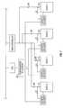
- FIG. 1is a diagram illustrating a reconfigurable chip 20 of the present invention.
- Reconfigurable chip 20is connected to an external memory 22 .
- Data from external memory 22is loaded into the reconfigurable chip 20 using the memory control 24 and Data Memory Access (DMA) controller 26 .
- the datais sent across an internal bus 28 .
- the external memorystores blocks 30 of data combined into a group 31 .
- Each block of dataincludes configuration bits 30 a and address bits 30 b .
- a group of blockscan store a downloadable configuration to implement a function for the reconfigurable computer.
- Configuration data blocksare sent to the memory controller across bus 28 to the data controller 26 .
- the blockis then sent to bus 32 .
- the bus 32splits into the address line 32 a and the configuration bit lines 32 b .
- the address lines 32 aare sent to address decoder 40 .
- the address decoderproduces select lines 42 which are sent to the reconfigurable logic along with the configuration bits along lines 32 b .
- the address decoder 40can also include a base offset address for the address decoder.
- the configuration bits on lines 32 bare loaded into a row of configuration memory associated with the active select line. Details of this arrangement are shown below in FIGS. 2-4.
- FIG. 2illustrates the data on the bus including twelve address bits and one hundred and sixteen configuration bits.
- FIG. 3shows the address decoder 50 receiving the address bits.
- the configuration bits and select lines produced by the address decoderare both supplied to a number of memory elements that are used to store the configuration data for the system. Depending upon which select line is active, a row of memory elements are loaded with the configuration bits on the configuration bit lines.
- FIG. 4illustrates a memory element 52 which can be located at the intersections of the select lines and configuration bits shown in FIG. 3 .
- the memory element 52produces a configuration bit output on line 54 .
- the memory elementalso receives a write select line from the address decoder and a configuration bit line. When the write select line goes high, data on the configuration bit line is stored in the memory element 52 .
- FIG. 5illustrates an embodiment of a one type of memory element that can be used with the present invention.
- the memory element 60includes a background plane latch and a foreground plane latch. Two different planes of configuration data are stored.
- the nodes 63 and 66store the foreground plane bit and the background plane bit respectively.
- the write select line to multiplexer 62goes high, data on the data input line 61 is written into the node 66 .
- the write select line to multiplexer 64goes high, the value at node 66 is loaded into node 63 . This causes the background plane to be loaded into the foreground plane.
- the reset line 70can be used to reset the node 66 and 63 to zero.
- FIG. 7illustrates an alternate embodiment of the present invention.
- multiple address decodersare used.
- a configuration allocation block 80is used to produce signals to the address decoders to cause the loading of the configurations.
- different functions configurationscan be dynamically loaded into different slices of the reconfigurable logic. An example of this type of system is described in the patent application, “Configuration Loading And Slice Allocation,” Ser. No. 09/507,344, which is incorporated herein by reference.
- FIGS. 6A-6Cillustrate an embodiment of the configuration data arrangement for one embodiment of the present invention. As described above not all of the lines of configuration data need to be stored in each downloaded group.
- the advantage of the present inventionis the address for part of the configuration data is stored along with the block including configuration bits.
- the full configurationneed always be downloaded. Some configuration bits in a slice or the entire reconfigurable logic may need only to be zeroed which can be done by a reset signal. Alternately, for reconfigurable computing, only parts of the reconfigurable logic may need be written over with the configuration data during the active processing. Thus, to implement certain functions, not all the configuration bits need to be loaded, and thus, not all the configuration bits need to be stored in the external memory.
Landscapes
- Engineering & Computer Science (AREA)
- Computer Hardware Design (AREA)
- Theoretical Computer Science (AREA)
- Physics & Mathematics (AREA)
- General Engineering & Computer Science (AREA)
- General Physics & Mathematics (AREA)
- Logic Circuits (AREA)
Abstract
Description
Claims (22)
Priority Applications (3)
| Application Number | Priority Date | Filing Date | Title |
|---|---|---|---|
| US09/507,337US6519674B1 (en) | 2000-02-18 | 2000-02-18 | Configuration bits layout |
| PCT/US2001/005283WO2001061497A1 (en) | 2000-02-18 | 2001-02-16 | Configuration bits layout |
| AU2001241567AAU2001241567A1 (en) | 2000-02-18 | 2001-02-16 | Configuration bits layout |
Applications Claiming Priority (1)
| Application Number | Priority Date | Filing Date | Title |
|---|---|---|---|
| US09/507,337US6519674B1 (en) | 2000-02-18 | 2000-02-18 | Configuration bits layout |
Publications (1)
| Publication Number | Publication Date |
|---|---|
| US6519674B1true US6519674B1 (en) | 2003-02-11 |
Family
ID=24018242
Family Applications (1)
| Application Number | Title | Priority Date | Filing Date |
|---|---|---|---|
| US09/507,337Expired - LifetimeUS6519674B1 (en) | 2000-02-18 | 2000-02-18 | Configuration bits layout |
Country Status (3)
| Country | Link |
|---|---|
| US (1) | US6519674B1 (en) |
| AU (1) | AU2001241567A1 (en) |
| WO (1) | WO2001061497A1 (en) |
Cited By (71)
| Publication number | Priority date | Publication date | Assignee | Title |
|---|---|---|---|---|
| US20030046607A1 (en)* | 2001-09-03 | 2003-03-06 | Frank May | Method for debugging reconfigurable architectures |
| US20030056202A1 (en)* | 2001-08-16 | 2003-03-20 | Frank May | Method for translating programs for reconfigurable architectures |
| US20030056085A1 (en)* | 1996-12-09 | 2003-03-20 | Entire Interest | Unit for processing numeric and logic operations for use in central processing units (CPUS), multiprocessor systems, data-flow processors (DSPS), systolic processors and field programmable gate arrays (FPGAS) |
| US20030093662A1 (en)* | 1996-12-27 | 2003-05-15 | Pact Gmbh | Process for automatic dynamic reloading of data flow processors (DFPS) and units with two- or three-dimensional programmable cell architectures (FPGAS, DPGAS, and the like) |
| US20030135686A1 (en)* | 1997-02-11 | 2003-07-17 | Martin Vorbach | Internal bus system for DFPs and units with two- or multi-dimensional programmable cell architectures, for managing large volumes of data with a high interconnection complexity |
| US20040015899A1 (en)* | 2000-10-06 | 2004-01-22 | Frank May | Method for processing data |
| US20040052130A1 (en)* | 1997-02-08 | 2004-03-18 | Martin Vorbach | Method of self-synchronization of configurable elements of a programmable unit |
| US20040083399A1 (en)* | 1997-02-08 | 2004-04-29 | Martin Vorbach | Method of self-synchronization of configurable elements of a programmable module |
| US6772230B2 (en)* | 2000-05-26 | 2004-08-03 | Lattice Semiconductor Corp. | Field programmable gate array (FPGA) bit stream format |
| US20040181726A1 (en)* | 1997-12-22 | 2004-09-16 | Martin Vorbach | Method and system for alternating between programs for execution by cells of an integrated circuit |
| US20040243984A1 (en)* | 2001-06-20 | 2004-12-02 | Martin Vorbach | Data processing method |
| US20040249880A1 (en)* | 2001-12-14 | 2004-12-09 | Martin Vorbach | Reconfigurable system |
| US20050053056A1 (en)* | 2001-09-03 | 2005-03-10 | Martin Vorbach | Router |
| US20050066213A1 (en)* | 2001-03-05 | 2005-03-24 | Martin Vorbach | Methods and devices for treating and processing data |
| US20050132344A1 (en)* | 2002-01-18 | 2005-06-16 | Martin Vorbach | Method of compilation |
| US20050144212A1 (en)* | 2003-12-29 | 2005-06-30 | Xilinx, Inc. | Programmable logic device with cascading DSP slices |
| US20050144211A1 (en)* | 2003-12-29 | 2005-06-30 | Xilinx, Inc. | Programmable logic device with pipelined DSP slices |
| US20050144215A1 (en)* | 2003-12-29 | 2005-06-30 | Xilinx, Inc. | Applications of cascading DSP slices |
| US20050144216A1 (en)* | 2003-12-29 | 2005-06-30 | Xilinx, Inc. | Arithmetic circuit with multiplexed addend inputs |
| US20050144210A1 (en)* | 2003-12-29 | 2005-06-30 | Xilinx, Inc. | Programmable logic device with dynamic DSP architecture |
| US20050223212A1 (en)* | 2000-06-13 | 2005-10-06 | Martin Vorbach | Pipeline configuration protocol and configuration unit communication |
| US6990555B2 (en) | 2001-01-09 | 2006-01-24 | Pact Xpp Technologies Ag | Method of hierarchical caching of configuration data having dataflow processors and modules having two- or multidimensional programmable cell structure (FPGAs, DPGAs, etc.) |
| US20060031595A1 (en)* | 1996-12-27 | 2006-02-09 | Martin Vorbach | Process for automatic dynamic reloading of data flow processors (DFPs) and units with two- or three-dimensional programmable cell architectures (FPGAs, DPGAs, and the like |
| US20060075211A1 (en)* | 2002-03-21 | 2006-04-06 | Martin Vorbach | Method and device for data processing |
| US20060090062A1 (en)* | 2002-01-19 | 2006-04-27 | Martin Vorbach | Reconfigurable processor |
| US20060190516A1 (en)* | 2003-12-29 | 2006-08-24 | Xilinx, Inc. | Digital signal processing element having an arithmetic logic unit |
| US20060192586A1 (en)* | 2002-09-06 | 2006-08-31 | Martin Vorbach | Reconfigurable sequencer structure |
| US20060195496A1 (en)* | 2003-12-29 | 2006-08-31 | Xilinx, Inc. | Digital signal processing circuit having a pattern detector circuit |
| US20060206557A1 (en)* | 2003-12-29 | 2006-09-14 | Xilinx, Inc. | Arithmetic logic unit circuit |
| US20060212499A1 (en)* | 2003-12-29 | 2006-09-21 | Xilinx, Inc. | Digital signal processing block having a wide multiplexer |
| US20060230096A1 (en)* | 2003-12-29 | 2006-10-12 | Xilinx, Inc. | Digital signal processing circuit having an adder circuit with carry-outs |
| US20060230095A1 (en)* | 2003-12-29 | 2006-10-12 | Xilinx, Inc. | Digital signal processing circuit having a pre-adder circuit |
| US20060230092A1 (en)* | 2003-12-29 | 2006-10-12 | Xilinx, Inc. | Architectural floorplan for a digital signal processing circuit |
| US20060248317A1 (en)* | 2002-08-07 | 2006-11-02 | Martin Vorbach | Method and device for processing data |
| US20060288070A1 (en)* | 2003-12-29 | 2006-12-21 | Xilinx, Inc. | Digital signal processing circuit having a pattern circuit for determining termination conditions |
| US20060288069A1 (en)* | 2003-12-29 | 2006-12-21 | Xilinx, Inc. | Digital signal processing circuit having a SIMD circuit |
| US20070011433A1 (en)* | 2003-04-04 | 2007-01-11 | Martin Vorbach | Method and device for data processing |
| US7174443B1 (en) | 1996-12-20 | 2007-02-06 | Pact Xpp Technologies Ag | Run-time reconfiguration method for programmable units |
| US20070050603A1 (en)* | 2002-08-07 | 2007-03-01 | Martin Vorbach | Data processing method and device |
| US20070113046A1 (en)* | 2001-03-05 | 2007-05-17 | Martin Vorbach | Data processing device and method |
| US20070123091A1 (en)* | 2005-11-18 | 2007-05-31 | Swedberg Benjamin D | Releasable Wire Connector |
| US20080222329A1 (en)* | 1996-12-20 | 2008-09-11 | Martin Vorbach | I/O and memory bus system for DFPs and units with two- or multi-dimensional programmable cell architectures |
| US20090031104A1 (en)* | 2005-02-07 | 2009-01-29 | Martin Vorbach | Low Latency Massive Parallel Data Processing Device |
| US20090146691A1 (en)* | 2000-10-06 | 2009-06-11 | Martin Vorbach | Logic cell array and bus system |
| US20090210653A1 (en)* | 2001-03-05 | 2009-08-20 | Pact Xpp Technologies Ag | Method and device for treating and processing data |
| US7581076B2 (en) | 2001-03-05 | 2009-08-25 | Pact Xpp Technologies Ag | Methods and devices for treating and/or processing data |
| US7595659B2 (en) | 2000-10-09 | 2009-09-29 | Pact Xpp Technologies Ag | Logic cell array and bus system |
| US20090300262A1 (en)* | 2001-03-05 | 2009-12-03 | Martin Vorbach | Methods and devices for treating and/or processing data |
| US20100153654A1 (en)* | 2002-08-07 | 2010-06-17 | Martin Vorbach | Data processing method and device |
| US20100192118A1 (en)* | 2009-01-27 | 2010-07-29 | Xilinx, Inc. | Method of and circuit for implementing a filter in an integrated circuit |
| US20100191786A1 (en)* | 2009-01-27 | 2010-07-29 | Xilinx, Inc. | Digital signal processing block with preadder stage |
| US20100228918A1 (en)* | 1999-06-10 | 2010-09-09 | Martin Vorbach | Configurable logic integrated circuit having a multidimensional structure of configurable elements |
| US20100241823A1 (en)* | 2003-08-28 | 2010-09-23 | Martin Vorbach | Data processing device and method |
| US7840627B2 (en) | 2003-12-29 | 2010-11-23 | Xilinx, Inc. | Digital signal processing circuit having input register blocks |
| US7853636B2 (en) | 2003-12-29 | 2010-12-14 | Xilinx, Inc. | Digital signal processing circuit having a pattern detector circuit for convergent rounding |
| US20110060942A1 (en)* | 2001-03-05 | 2011-03-10 | Martin Vorbach | Methods and devices for treating and/or processing data |
| US7996827B2 (en)* | 2001-08-16 | 2011-08-09 | Martin Vorbach | Method for the translation of programs for reconfigurable architectures |
| US20110238948A1 (en)* | 2002-08-07 | 2011-09-29 | Martin Vorbach | Method and device for coupling a data processing unit and a data processing array |
| US8127061B2 (en) | 2002-02-18 | 2012-02-28 | Martin Vorbach | Bus systems and reconfiguration methods |
| US8222923B1 (en)* | 2009-01-31 | 2012-07-17 | Xilinx, Inc. | Method and apparatus for memory control with a programmable device |
| US8250503B2 (en) | 2006-01-18 | 2012-08-21 | Martin Vorbach | Hardware definition method including determining whether to implement a function as hardware or software |
| US8686549B2 (en) | 2001-09-03 | 2014-04-01 | Martin Vorbach | Reconfigurable elements |
| US8686475B2 (en) | 2001-09-19 | 2014-04-01 | Pact Xpp Technologies Ag | Reconfigurable elements |
| US8922243B2 (en)* | 2012-12-23 | 2014-12-30 | Advanced Micro Devices, Inc. | Die-stacked memory device with reconfigurable logic |
| US9065722B2 (en) | 2012-12-23 | 2015-06-23 | Advanced Micro Devices, Inc. | Die-stacked device with partitioned multi-hop network |
| US9135185B2 (en) | 2012-12-23 | 2015-09-15 | Advanced Micro Devices, Inc. | Die-stacked memory device providing data translation |
| US9170948B2 (en) | 2012-12-23 | 2015-10-27 | Advanced Micro Devices, Inc. | Cache coherency using die-stacked memory device with logic die |
| US9201777B2 (en) | 2012-12-23 | 2015-12-01 | Advanced Micro Devices, Inc. | Quality of service support using stacked memory device with logic die |
| US9286948B2 (en) | 2013-07-15 | 2016-03-15 | Advanced Micro Devices, Inc. | Query operations for stacked-die memory device |
| US9697147B2 (en) | 2012-08-06 | 2017-07-04 | Advanced Micro Devices, Inc. | Stacked memory device with metadata management |
| CN109857701A (en)* | 2018-02-27 | 2019-06-07 | 上海安路信息科技有限公司 | The activation system and its method of FPGA configuration circuit |
Citations (15)
| Publication number | Priority date | Publication date | Assignee | Title |
|---|---|---|---|---|
| US5430687A (en) | 1994-04-01 | 1995-07-04 | Xilinx, Inc. | Programmable logic device including a parallel input device for loading memory cells |
| US5457408A (en)* | 1994-11-23 | 1995-10-10 | At&T Corp. | Method and apparatus for verifying whether a bitstream received by a field programmable gate array (FPGA) is intended for that FPGA |
| US5493239A (en) | 1995-01-31 | 1996-02-20 | Motorola, Inc. | Circuit and method of configuring a field programmable gate array |
| US5705938A (en)* | 1995-05-02 | 1998-01-06 | Xilinx, Inc. | Programmable switch for FPGA input/output signals |
| US5732246A (en) | 1995-06-07 | 1998-03-24 | International Business Machines Corporation | Programmable array interconnect latch |
| US5802003A (en) | 1995-12-20 | 1998-09-01 | International Business Machines Corporation | System for implementing write, initialization, and reset in a memory array using a single cell write port |
| US5821772A (en)* | 1996-08-07 | 1998-10-13 | Xilinx, Inc. | Programmable address decoder for programmable logic device |
| US5910732A (en)* | 1997-03-12 | 1999-06-08 | Xilinx, Inc. | Programmable gate array having shared signal lines for interconnect and configuration |
| US6020758A (en)* | 1996-03-11 | 2000-02-01 | Altera Corporation | Partially reconfigurable programmable logic device |
| US6172521B1 (en)* | 1997-04-11 | 2001-01-09 | Nec Corporation | Programmable logic IC having memories for previously storing a plurality of configuration data and a method of reconfigurating same |
| US6172520B1 (en)* | 1997-12-30 | 2001-01-09 | Xilinx, Inc. | FPGA system with user-programmable configuration ports and method for reconfiguring the FPGA |
| US6204687B1 (en)* | 1999-08-13 | 2001-03-20 | Xilinx, Inc. | Method and structure for configuring FPGAS |
| US6222757B1 (en)* | 1998-02-25 | 2001-04-24 | Xilinx, Inc. | Configuration memory architecture for FPGA |
| US6255848B1 (en)* | 1999-04-05 | 2001-07-03 | Xilinx, Inc. | Method and structure for reading, modifying and writing selected configuration memory cells of an FPGA |
| US6262596B1 (en)* | 1999-04-05 | 2001-07-17 | Xilinx, Inc. | Configuration bus interface circuit for FPGAS |
- 2000
- 2000-02-18USUS09/507,337patent/US6519674B1/ennot_activeExpired - Lifetime
- 2001
- 2001-02-16AUAU2001241567Apatent/AU2001241567A1/ennot_activeAbandoned
- 2001-02-16WOPCT/US2001/005283patent/WO2001061497A1/enactiveApplication Filing
Patent Citations (16)
| Publication number | Priority date | Publication date | Assignee | Title |
|---|---|---|---|---|
| US5430687A (en) | 1994-04-01 | 1995-07-04 | Xilinx, Inc. | Programmable logic device including a parallel input device for loading memory cells |
| US5457408A (en)* | 1994-11-23 | 1995-10-10 | At&T Corp. | Method and apparatus for verifying whether a bitstream received by a field programmable gate array (FPGA) is intended for that FPGA |
| US5493239A (en) | 1995-01-31 | 1996-02-20 | Motorola, Inc. | Circuit and method of configuring a field programmable gate array |
| US5705938A (en)* | 1995-05-02 | 1998-01-06 | Xilinx, Inc. | Programmable switch for FPGA input/output signals |
| US5732246A (en) | 1995-06-07 | 1998-03-24 | International Business Machines Corporation | Programmable array interconnect latch |
| US5802003A (en) | 1995-12-20 | 1998-09-01 | International Business Machines Corporation | System for implementing write, initialization, and reset in a memory array using a single cell write port |
| US6020758A (en)* | 1996-03-11 | 2000-02-01 | Altera Corporation | Partially reconfigurable programmable logic device |
| US5821772A (en)* | 1996-08-07 | 1998-10-13 | Xilinx, Inc. | Programmable address decoder for programmable logic device |
| US5910732A (en)* | 1997-03-12 | 1999-06-08 | Xilinx, Inc. | Programmable gate array having shared signal lines for interconnect and configuration |
| US6037800A (en)* | 1997-03-12 | 2000-03-14 | Xilinx, Inc. | Method for programming a programmable gate array having shared signal lines for interconnect and configuration |
| US6172521B1 (en)* | 1997-04-11 | 2001-01-09 | Nec Corporation | Programmable logic IC having memories for previously storing a plurality of configuration data and a method of reconfigurating same |
| US6172520B1 (en)* | 1997-12-30 | 2001-01-09 | Xilinx, Inc. | FPGA system with user-programmable configuration ports and method for reconfiguring the FPGA |
| US6222757B1 (en)* | 1998-02-25 | 2001-04-24 | Xilinx, Inc. | Configuration memory architecture for FPGA |
| US6255848B1 (en)* | 1999-04-05 | 2001-07-03 | Xilinx, Inc. | Method and structure for reading, modifying and writing selected configuration memory cells of an FPGA |
| US6262596B1 (en)* | 1999-04-05 | 2001-07-17 | Xilinx, Inc. | Configuration bus interface circuit for FPGAS |
| US6204687B1 (en)* | 1999-08-13 | 2001-03-20 | Xilinx, Inc. | Method and structure for configuring FPGAS |
Cited By (167)
| Publication number | Priority date | Publication date | Assignee | Title |
|---|---|---|---|---|
| US20040168099A1 (en)* | 1996-12-09 | 2004-08-26 | Martin Vorbach | Unit for processing numeric and logic operations for use in central processing units (CPUs), multiprocessor systems |
| US20110010523A1 (en)* | 1996-12-09 | 2011-01-13 | Martin Vorbach | Runtime configurable arithmetic and logic cell |
| US20030056085A1 (en)* | 1996-12-09 | 2003-03-20 | Entire Interest | Unit for processing numeric and logic operations for use in central processing units (CPUS), multiprocessor systems, data-flow processors (DSPS), systolic processors and field programmable gate arrays (FPGAS) |
| US7565525B2 (en) | 1996-12-09 | 2009-07-21 | Pact Xpp Technologies Ag | Runtime configurable arithmetic and logic cell |
| US20080010437A1 (en)* | 1996-12-09 | 2008-01-10 | Martin Vorbach | Unit for processing numeric and logic operations for use in central processing units (CPUS), multiprocessor systems, data-flow processors (DSPS), systolic processors and field programmable gate arrays (FPGAS) |
| US7237087B2 (en) | 1996-12-09 | 2007-06-26 | Pact Xpp Technologies Ag | Reconfigurable multidimensional array processor allowing runtime reconfiguration of selected individual array cells |
| US7822968B2 (en) | 1996-12-09 | 2010-10-26 | Martin Vorbach | Circuit having a multidimensional structure of configurable cells that include multi-bit-wide inputs and outputs |
| US20090146690A1 (en)* | 1996-12-09 | 2009-06-11 | Martin Vorbach | Runtime configurable arithmetic and logic cell |
| US8156312B2 (en) | 1996-12-09 | 2012-04-10 | Martin Vorbach | Processor chip for reconfigurable data processing, for processing numeric and logic operations and including function and interconnection control units |
| US20080222329A1 (en)* | 1996-12-20 | 2008-09-11 | Martin Vorbach | I/O and memory bus system for DFPs and units with two- or multi-dimensional programmable cell architectures |
| US8195856B2 (en) | 1996-12-20 | 2012-06-05 | Martin Vorbach | I/O and memory bus system for DFPS and units with two- or multi-dimensional programmable cell architectures |
| US20100287318A1 (en)* | 1996-12-20 | 2010-11-11 | Martin Vorbach | I/o and memory bus system for dfps and units with two- or multi-dimensional programmable cell architectures |
| US7174443B1 (en) | 1996-12-20 | 2007-02-06 | Pact Xpp Technologies Ag | Run-time reconfiguration method for programmable units |
| US7899962B2 (en) | 1996-12-20 | 2011-03-01 | Martin Vorbach | I/O and memory bus system for DFPs and units with two- or multi-dimensional programmable cell architectures |
| US20100082863A1 (en)* | 1996-12-20 | 2010-04-01 | Martin Vorbach | I/O AND MEMORY BUS SYSTEM FOR DFPs AND UNITS WITH TWO- OR MULTI-DIMENSIONAL PROGRAMMABLE CELL ARCHITECTURES |
| US7650448B2 (en) | 1996-12-20 | 2010-01-19 | Pact Xpp Technologies Ag | I/O and memory bus system for DFPS and units with two- or multi-dimensional programmable cell architectures |
| US7822881B2 (en) | 1996-12-27 | 2010-10-26 | Martin Vorbach | Process for automatic dynamic reloading of data flow processors (DFPs) and units with two- or three-dimensional programmable cell architectures (FPGAs, DPGAs, and the like) |
| US20090153188A1 (en)* | 1996-12-27 | 2009-06-18 | Martin Vorbach | PROCESS FOR AUTOMATIC DYNAMIC RELOADING OF DATA FLOW PROCESSORS (DFPs) AND UNITS WITH TWO- OR THREE-DIMENSIONAL PROGRAMMABLE CELL ARCHITECTURES (FPGAs, DPGAs AND THE LIKE) |
| US20030093662A1 (en)* | 1996-12-27 | 2003-05-15 | Pact Gmbh | Process for automatic dynamic reloading of data flow processors (DFPS) and units with two- or three-dimensional programmable cell architectures (FPGAS, DPGAS, and the like) |
| US7028107B2 (en) | 1996-12-27 | 2006-04-11 | Pact Xpp Technologies Ag | Process for automatic dynamic reloading of data flow processors (DFPS) and units with two- or three- dimensional programmable cell architectures (FPGAS, DPGAS, and the like) |
| US20060031595A1 (en)* | 1996-12-27 | 2006-02-09 | Martin Vorbach | Process for automatic dynamic reloading of data flow processors (DFPs) and units with two- or three-dimensional programmable cell architectures (FPGAs, DPGAs, and the like |
| US6968452B2 (en) | 1997-02-08 | 2005-11-22 | Pact Xpp Technologies Ag | Method of self-synchronization of configurable elements of a programmable unit |
| USRE44383E1 (en) | 1997-02-08 | 2013-07-16 | Martin Vorbach | Method of self-synchronization of configurable elements of a programmable module |
| USRE44365E1 (en) | 1997-02-08 | 2013-07-09 | Martin Vorbach | Method of self-synchronization of configurable elements of a programmable module |
| US20040083399A1 (en)* | 1997-02-08 | 2004-04-29 | Martin Vorbach | Method of self-synchronization of configurable elements of a programmable module |
| USRE45223E1 (en) | 1997-02-08 | 2014-10-28 | Pact Xpp Technologies Ag | Method of self-synchronization of configurable elements of a programmable module |
| US20040052130A1 (en)* | 1997-02-08 | 2004-03-18 | Martin Vorbach | Method of self-synchronization of configurable elements of a programmable unit |
| USRE45109E1 (en) | 1997-02-08 | 2014-09-02 | Pact Xpp Technologies Ag | Method of self-synchronization of configurable elements of a programmable module |
| US7036036B2 (en) | 1997-02-08 | 2006-04-25 | Pact Xpp Technologies Ag | Method of self-synchronization of configurable elements of a programmable module |
| US7010667B2 (en)* | 1997-02-11 | 2006-03-07 | Pact Xpp Technologies Ag | Internal bus system for DFPS and units with two- or multi-dimensional programmable cell architectures, for managing large volumes of data with a high interconnection complexity |
| US20030135686A1 (en)* | 1997-02-11 | 2003-07-17 | Martin Vorbach | Internal bus system for DFPs and units with two- or multi-dimensional programmable cell architectures, for managing large volumes of data with a high interconnection complexity |
| US20090300445A1 (en)* | 1997-12-22 | 2009-12-03 | Martin Vorbach | Method and system for alternating between programs for execution by cells of an integrated circuit |
| US8819505B2 (en) | 1997-12-22 | 2014-08-26 | Pact Xpp Technologies Ag | Data processor having disabled cores |
| US20040181726A1 (en)* | 1997-12-22 | 2004-09-16 | Martin Vorbach | Method and system for alternating between programs for execution by cells of an integrated circuit |
| US8468329B2 (en) | 1999-02-25 | 2013-06-18 | Martin Vorbach | Pipeline configuration protocol and configuration unit communication |
| US8312200B2 (en) | 1999-06-10 | 2012-11-13 | Martin Vorbach | Processor chip including a plurality of cache elements connected to a plurality of processor cores |
| US8726250B2 (en) | 1999-06-10 | 2014-05-13 | Pact Xpp Technologies Ag | Configurable logic integrated circuit having a multidimensional structure of configurable elements |
| US20100228918A1 (en)* | 1999-06-10 | 2010-09-09 | Martin Vorbach | Configurable logic integrated circuit having a multidimensional structure of configurable elements |
| US8230411B1 (en) | 1999-06-10 | 2012-07-24 | Martin Vorbach | Method for interleaving a program over a plurality of cells |
| US6772230B2 (en)* | 2000-05-26 | 2004-08-03 | Lattice Semiconductor Corp. | Field programmable gate array (FPGA) bit stream format |
| US7003660B2 (en) | 2000-06-13 | 2006-02-21 | Pact Xpp Technologies Ag | Pipeline configuration unit protocols and communication |
| US8301872B2 (en) | 2000-06-13 | 2012-10-30 | Martin Vorbach | Pipeline configuration protocol and configuration unit communication |
| US20050223212A1 (en)* | 2000-06-13 | 2005-10-06 | Martin Vorbach | Pipeline configuration protocol and configuration unit communication |
| US9047440B2 (en) | 2000-10-06 | 2015-06-02 | Pact Xpp Technologies Ag | Logical cell array and bus system |
| US8471593B2 (en) | 2000-10-06 | 2013-06-25 | Martin Vorbach | Logic cell array and bus system |
| US20090146691A1 (en)* | 2000-10-06 | 2009-06-11 | Martin Vorbach | Logic cell array and bus system |
| US8058899B2 (en) | 2000-10-06 | 2011-11-15 | Martin Vorbach | Logic cell array and bus system |
| US20040015899A1 (en)* | 2000-10-06 | 2004-01-22 | Frank May | Method for processing data |
| US7595659B2 (en) | 2000-10-09 | 2009-09-29 | Pact Xpp Technologies Ag | Logic cell array and bus system |
| US6990555B2 (en) | 2001-01-09 | 2006-01-24 | Pact Xpp Technologies Ag | Method of hierarchical caching of configuration data having dataflow processors and modules having two- or multidimensional programmable cell structure (FPGAs, DPGAs, etc.) |
| US8312301B2 (en) | 2001-03-05 | 2012-11-13 | Martin Vorbach | Methods and devices for treating and processing data |
| US9075605B2 (en) | 2001-03-05 | 2015-07-07 | Pact Xpp Technologies Ag | Methods and devices for treating and processing data |
| US7844796B2 (en) | 2001-03-05 | 2010-11-30 | Martin Vorbach | Data processing device and method |
| US20070113046A1 (en)* | 2001-03-05 | 2007-05-17 | Martin Vorbach | Data processing device and method |
| US20050066213A1 (en)* | 2001-03-05 | 2005-03-24 | Martin Vorbach | Methods and devices for treating and processing data |
| US20110060942A1 (en)* | 2001-03-05 | 2011-03-10 | Martin Vorbach | Methods and devices for treating and/or processing data |
| US20110173389A1 (en)* | 2001-03-05 | 2011-07-14 | Martin Vorbach | Methods and devices for treating and/or processing data |
| US7444531B2 (en) | 2001-03-05 | 2008-10-28 | Pact Xpp Technologies Ag | Methods and devices for treating and processing data |
| US8099618B2 (en) | 2001-03-05 | 2012-01-17 | Martin Vorbach | Methods and devices for treating and processing data |
| US20100023796A1 (en)* | 2001-03-05 | 2010-01-28 | Martin Vorbach | Methods and devices for treating and processing data |
| US9037807B2 (en) | 2001-03-05 | 2015-05-19 | Pact Xpp Technologies Ag | Processor arrangement on a chip including data processing, memory, and interface elements |
| US20090300262A1 (en)* | 2001-03-05 | 2009-12-03 | Martin Vorbach | Methods and devices for treating and/or processing data |
| US7581076B2 (en) | 2001-03-05 | 2009-08-25 | Pact Xpp Technologies Ag | Methods and devices for treating and/or processing data |
| US20090210653A1 (en)* | 2001-03-05 | 2009-08-20 | Pact Xpp Technologies Ag | Method and device for treating and processing data |
| US20090100286A1 (en)* | 2001-03-05 | 2009-04-16 | Martin Vorbach | Methods and devices for treating and processing data |
| US20090144522A1 (en)* | 2001-03-05 | 2009-06-04 | Martin Vorbach | Data Processing Device and Method |
| US8145881B2 (en) | 2001-03-05 | 2012-03-27 | Martin Vorbach | Data processing device and method |
| US20040243984A1 (en)* | 2001-06-20 | 2004-12-02 | Martin Vorbach | Data processing method |
| US20100095094A1 (en)* | 2001-06-20 | 2010-04-15 | Martin Vorbach | Method for processing data |
| US7657877B2 (en) | 2001-06-20 | 2010-02-02 | Pact Xpp Technologies Ag | Method for processing data |
| US8869121B2 (en) | 2001-08-16 | 2014-10-21 | Pact Xpp Technologies Ag | Method for the translation of programs for reconfigurable architectures |
| US20030056202A1 (en)* | 2001-08-16 | 2003-03-20 | Frank May | Method for translating programs for reconfigurable architectures |
| US7210129B2 (en) | 2001-08-16 | 2007-04-24 | Pact Xpp Technologies Ag | Method for translating programs for reconfigurable architectures |
| US7996827B2 (en)* | 2001-08-16 | 2011-08-09 | Martin Vorbach | Method for the translation of programs for reconfigurable architectures |
| US20030046607A1 (en)* | 2001-09-03 | 2003-03-06 | Frank May | Method for debugging reconfigurable architectures |
| US8407525B2 (en) | 2001-09-03 | 2013-03-26 | Pact Xpp Technologies Ag | Method for debugging reconfigurable architectures |
| US7840842B2 (en) | 2001-09-03 | 2010-11-23 | Martin Vorbach | Method for debugging reconfigurable architectures |
| US7480825B2 (en) | 2001-09-03 | 2009-01-20 | Pact Xpp Technologies Ag | Method for debugging reconfigurable architectures |
| US8686549B2 (en) | 2001-09-03 | 2014-04-01 | Martin Vorbach | Reconfigurable elements |
| US8429385B2 (en) | 2001-09-03 | 2013-04-23 | Martin Vorbach | Device including a field having function cells and information providing cells controlled by the function cells |
| US8209653B2 (en) | 2001-09-03 | 2012-06-26 | Martin Vorbach | Router |
| US20050053056A1 (en)* | 2001-09-03 | 2005-03-10 | Martin Vorbach | Router |
| US20090037865A1 (en)* | 2001-09-03 | 2009-02-05 | Martin Vorbach | Router |
| US8069373B2 (en) | 2001-09-03 | 2011-11-29 | Martin Vorbach | Method for debugging reconfigurable architectures |
| US7266725B2 (en) | 2001-09-03 | 2007-09-04 | Pact Xpp Technologies Ag | Method for debugging reconfigurable architectures |
| US20090150725A1 (en)* | 2001-09-03 | 2009-06-11 | Martin Vorbach | Method for debugging reconfigurable architectures |
| US7434191B2 (en) | 2001-09-03 | 2008-10-07 | Pact Xpp Technologies Ag | Router |
| US20050022062A1 (en)* | 2001-09-03 | 2005-01-27 | Martin Vorbach | Method for debugging reconfigurable architectures |
| US20060245225A1 (en)* | 2001-09-03 | 2006-11-02 | Martin Vorbach | Reconfigurable elements |
| US8686475B2 (en) | 2001-09-19 | 2014-04-01 | Pact Xpp Technologies Ag | Reconfigurable elements |
| US7577822B2 (en) | 2001-12-14 | 2009-08-18 | Pact Xpp Technologies Ag | Parallel task operation in processor and reconfigurable coprocessor configured based on information in link list including termination information for synchronization |
| US20040249880A1 (en)* | 2001-12-14 | 2004-12-09 | Martin Vorbach | Reconfigurable system |
| US20050132344A1 (en)* | 2002-01-18 | 2005-06-16 | Martin Vorbach | Method of compilation |
| US8281108B2 (en) | 2002-01-19 | 2012-10-02 | Martin Vorbach | Reconfigurable general purpose processor having time restricted configurations |
| US20060090062A1 (en)* | 2002-01-19 | 2006-04-27 | Martin Vorbach | Reconfigurable processor |
| US8127061B2 (en) | 2002-02-18 | 2012-02-28 | Martin Vorbach | Bus systems and reconfiguration methods |
| US20100174868A1 (en)* | 2002-03-21 | 2010-07-08 | Martin Vorbach | Processor device having a sequential data processing unit and an arrangement of data processing elements |
| US20060075211A1 (en)* | 2002-03-21 | 2006-04-06 | Martin Vorbach | Method and device for data processing |
| US20060248317A1 (en)* | 2002-08-07 | 2006-11-02 | Martin Vorbach | Method and device for processing data |
| US8281265B2 (en) | 2002-08-07 | 2012-10-02 | Martin Vorbach | Method and device for processing data |
| US8914590B2 (en) | 2002-08-07 | 2014-12-16 | Pact Xpp Technologies Ag | Data processing method and device |
| US20110238948A1 (en)* | 2002-08-07 | 2011-09-29 | Martin Vorbach | Method and device for coupling a data processing unit and a data processing array |
| US20100070671A1 (en)* | 2002-08-07 | 2010-03-18 | Martin Vorbach | Method and device for processing data |
| US7657861B2 (en) | 2002-08-07 | 2010-02-02 | Pact Xpp Technologies Ag | Method and device for processing data |
| US20100153654A1 (en)* | 2002-08-07 | 2010-06-17 | Martin Vorbach | Data processing method and device |
| US20070050603A1 (en)* | 2002-08-07 | 2007-03-01 | Martin Vorbach | Data processing method and device |
| US8156284B2 (en) | 2002-08-07 | 2012-04-10 | Martin Vorbach | Data processing method and device |
| US7602214B2 (en) | 2002-09-06 | 2009-10-13 | Pact Xpp Technologies Ag | Reconfigurable sequencer structure |
| US20110006805A1 (en)* | 2002-09-06 | 2011-01-13 | Martin Vorbach | Reconfigurable sequencer structure |
| US20080191737A1 (en)* | 2002-09-06 | 2008-08-14 | Martin Vorbach | Reconfigurable sequencer structure |
| US7394284B2 (en) | 2002-09-06 | 2008-07-01 | Pact Xpp Technologies Ag | Reconfigurable sequencer structure |
| US8310274B2 (en) | 2002-09-06 | 2012-11-13 | Martin Vorbach | Reconfigurable sequencer structure |
| US7782087B2 (en) | 2002-09-06 | 2010-08-24 | Martin Vorbach | Reconfigurable sequencer structure |
| US7928763B2 (en) | 2002-09-06 | 2011-04-19 | Martin Vorbach | Multi-core processing system |
| US20110148460A1 (en)* | 2002-09-06 | 2011-06-23 | Martin Vorbach | Reconfigurable sequencer structure |
| US8803552B2 (en) | 2002-09-06 | 2014-08-12 | Pact Xpp Technologies Ag | Reconfigurable sequencer structure |
| US20060192586A1 (en)* | 2002-09-06 | 2006-08-31 | Martin Vorbach | Reconfigurable sequencer structure |
| US20070011433A1 (en)* | 2003-04-04 | 2007-01-11 | Martin Vorbach | Method and device for data processing |
| US8812820B2 (en) | 2003-08-28 | 2014-08-19 | Pact Xpp Technologies Ag | Data processing device and method |
| US20100241823A1 (en)* | 2003-08-28 | 2010-09-23 | Martin Vorbach | Data processing device and method |
| US8495122B2 (en) | 2003-12-29 | 2013-07-23 | Xilinx, Inc. | Programmable device with dynamic DSP architecture |
| US7840627B2 (en) | 2003-12-29 | 2010-11-23 | Xilinx, Inc. | Digital signal processing circuit having input register blocks |
| US7567997B2 (en) | 2003-12-29 | 2009-07-28 | Xilinx, Inc. | Applications of cascading DSP slices |
| US7882165B2 (en) | 2003-12-29 | 2011-02-01 | Xilinx, Inc. | Digital signal processing element having an arithmetic logic unit |
| US20050144212A1 (en)* | 2003-12-29 | 2005-06-30 | Xilinx, Inc. | Programmable logic device with cascading DSP slices |
| US7480690B2 (en) | 2003-12-29 | 2009-01-20 | Xilinx, Inc. | Arithmetic circuit with multiplexed addend inputs |
| US7472155B2 (en) | 2003-12-29 | 2008-12-30 | Xilinx, Inc. | Programmable logic device with cascading DSP slices |
| US20050144211A1 (en)* | 2003-12-29 | 2005-06-30 | Xilinx, Inc. | Programmable logic device with pipelined DSP slices |
| US7467175B2 (en) | 2003-12-29 | 2008-12-16 | Xilinx, Inc. | Programmable logic device with pipelined DSP slices |
| US20050144215A1 (en)* | 2003-12-29 | 2005-06-30 | Xilinx, Inc. | Applications of cascading DSP slices |
| US7840630B2 (en) | 2003-12-29 | 2010-11-23 | Xilinx, Inc. | Arithmetic logic unit circuit |
| US7870182B2 (en) | 2003-12-29 | 2011-01-11 | Xilinx Inc. | Digital signal processing circuit having an adder circuit with carry-outs |
| US20060230096A1 (en)* | 2003-12-29 | 2006-10-12 | Xilinx, Inc. | Digital signal processing circuit having an adder circuit with carry-outs |
| US20050144216A1 (en)* | 2003-12-29 | 2005-06-30 | Xilinx, Inc. | Arithmetic circuit with multiplexed addend inputs |
| US7860915B2 (en) | 2003-12-29 | 2010-12-28 | Xilinx, Inc. | Digital signal processing circuit having a pattern circuit for determining termination conditions |
| US7853632B2 (en) | 2003-12-29 | 2010-12-14 | Xilinx, Inc. | Architectural floorplan for a digital signal processing circuit |
| US7853636B2 (en) | 2003-12-29 | 2010-12-14 | Xilinx, Inc. | Digital signal processing circuit having a pattern detector circuit for convergent rounding |
| US20060288069A1 (en)* | 2003-12-29 | 2006-12-21 | Xilinx, Inc. | Digital signal processing circuit having a SIMD circuit |
| US20060288070A1 (en)* | 2003-12-29 | 2006-12-21 | Xilinx, Inc. | Digital signal processing circuit having a pattern circuit for determining termination conditions |
| US20060230092A1 (en)* | 2003-12-29 | 2006-10-12 | Xilinx, Inc. | Architectural floorplan for a digital signal processing circuit |
| US20050144210A1 (en)* | 2003-12-29 | 2005-06-30 | Xilinx, Inc. | Programmable logic device with dynamic DSP architecture |
| US20060230095A1 (en)* | 2003-12-29 | 2006-10-12 | Xilinx, Inc. | Digital signal processing circuit having a pre-adder circuit |
| US7849119B2 (en) | 2003-12-29 | 2010-12-07 | Xilinx, Inc. | Digital signal processing circuit having a pattern detector circuit |
| US7865542B2 (en) | 2003-12-29 | 2011-01-04 | Xilinx, Inc. | Digital signal processing block having a wide multiplexer |
| US20060190516A1 (en)* | 2003-12-29 | 2006-08-24 | Xilinx, Inc. | Digital signal processing element having an arithmetic logic unit |
| US20060212499A1 (en)* | 2003-12-29 | 2006-09-21 | Xilinx, Inc. | Digital signal processing block having a wide multiplexer |
| US20060206557A1 (en)* | 2003-12-29 | 2006-09-14 | Xilinx, Inc. | Arithmetic logic unit circuit |
| US20060195496A1 (en)* | 2003-12-29 | 2006-08-31 | Xilinx, Inc. | Digital signal processing circuit having a pattern detector circuit |
| US7853634B2 (en) | 2003-12-29 | 2010-12-14 | Xilinx, Inc. | Digital signal processing circuit having a SIMD circuit |
| US7844653B2 (en) | 2003-12-29 | 2010-11-30 | Xilinx, Inc. | Digital signal processing circuit having a pre-adder circuit |
| US20090031104A1 (en)* | 2005-02-07 | 2009-01-29 | Martin Vorbach | Low Latency Massive Parallel Data Processing Device |
| US20070123091A1 (en)* | 2005-11-18 | 2007-05-31 | Swedberg Benjamin D | Releasable Wire Connector |
| US8250503B2 (en) | 2006-01-18 | 2012-08-21 | Martin Vorbach | Hardware definition method including determining whether to implement a function as hardware or software |
| US20100192118A1 (en)* | 2009-01-27 | 2010-07-29 | Xilinx, Inc. | Method of and circuit for implementing a filter in an integrated circuit |
| US8479133B2 (en) | 2009-01-27 | 2013-07-02 | Xilinx, Inc. | Method of and circuit for implementing a filter in an integrated circuit |
| US20100191786A1 (en)* | 2009-01-27 | 2010-07-29 | Xilinx, Inc. | Digital signal processing block with preadder stage |
| US8543635B2 (en) | 2009-01-27 | 2013-09-24 | Xilinx, Inc. | Digital signal processing block with preadder stage |
| US8222923B1 (en)* | 2009-01-31 | 2012-07-17 | Xilinx, Inc. | Method and apparatus for memory control with a programmable device |
| US9697147B2 (en) | 2012-08-06 | 2017-07-04 | Advanced Micro Devices, Inc. | Stacked memory device with metadata management |
| US9135185B2 (en) | 2012-12-23 | 2015-09-15 | Advanced Micro Devices, Inc. | Die-stacked memory device providing data translation |
| US9065722B2 (en) | 2012-12-23 | 2015-06-23 | Advanced Micro Devices, Inc. | Die-stacked device with partitioned multi-hop network |
| US9170948B2 (en) | 2012-12-23 | 2015-10-27 | Advanced Micro Devices, Inc. | Cache coherency using die-stacked memory device with logic die |
| US9201777B2 (en) | 2012-12-23 | 2015-12-01 | Advanced Micro Devices, Inc. | Quality of service support using stacked memory device with logic die |
| US8922243B2 (en)* | 2012-12-23 | 2014-12-30 | Advanced Micro Devices, Inc. | Die-stacked memory device with reconfigurable logic |
| US9286948B2 (en) | 2013-07-15 | 2016-03-15 | Advanced Micro Devices, Inc. | Query operations for stacked-die memory device |
| CN109857701A (en)* | 2018-02-27 | 2019-06-07 | 上海安路信息科技有限公司 | The activation system and its method of FPGA configuration circuit |
| CN109857701B (en)* | 2018-02-27 | 2023-06-27 | 上海安路信息科技股份有限公司 | Starting system and method for FPGA configuration circuit |
Also Published As
| Publication number | Publication date |
|---|---|
| AU2001241567A1 (en) | 2001-08-27 |
| WO2001061497A1 (en) | 2001-08-23 |
Similar Documents
| Publication | Publication Date | Title |
|---|---|---|
| US6519674B1 (en) | Configuration bits layout | |
| US4852048A (en) | Single instruction multiple data (SIMD) cellular array processing apparatus employing a common bus where a first number of bits manifest a first bus portion and a second number of bits manifest a second bus portion | |
| US5818350A (en) | High performance method of and system for selecting one of a plurality of IC chip while requiring minimal select lines | |
| US4835729A (en) | Single instruction multiple data (SIMD) cellular array processing apparatus with on-board RAM and address generator apparatus | |
| US4831519A (en) | Cellular array processor with variable nesting depth vector control by selective enabling of left and right neighboring processor cells | |
| US3772658A (en) | Electronic memory having a page swapping capability | |
| KR940000293B1 (en) | Simplified synchronous mesh processor | |
| US7617383B2 (en) | Circular register arrays of a computer | |
| US4916657A (en) | Single instruction multiple data (SIMD) cellular array processing apparatus employing multiple state logic for coupling to data buses | |
| US5802541A (en) | Method and apparatus in a data processing system for using chip selects to perform a memory management function | |
| CA2403675A1 (en) | Enhanced memory algorithmic processor architecture for multiprocessor computer systems | |
| US4783732A (en) | Two-wire/three-port RAM for cellular array processor | |
| US7679973B2 (en) | Register file | |
| US6460131B1 (en) | FPGA input output buffer with registered tristate enable | |
| US6212591B1 (en) | Configurable I/O circuitry defining virtual ports | |
| US6067267A (en) | Four-way interleaved FIFO architecture with look ahead conditional decoder for PCI applications | |
| US4761754A (en) | Vector processor wherein outputs of vector registers are fixedly coupled to inputs of vector calculators | |
| USRE37060E1 (en) | Apparatus for serial reading and writing of random access memory arrays | |
| US7386689B2 (en) | Method and apparatus for connecting a massively parallel processor array to a memory array in a bit serial manner | |
| EP0367995A2 (en) | Vector data transfer controller | |
| US5603046A (en) | Method for complex data movement in a multi-processor data processing system | |
| US4733393A (en) | Test method and apparatus for cellular array processor chip | |
| US6510483B1 (en) | Circuit, architecture and method for reading an address counter and/or matching a bus width through one or more synchronous ports | |
| JPS62156742A (en) | Data writing control system | |
| US6961280B1 (en) | Techniques for implementing address recycling in memory circuits |
Legal Events
| Date | Code | Title | Description |
|---|---|---|---|
| AS | Assignment | Owner name:CHAMELEON SYSTEMS, INC., CALIFORNIA Free format text:ASSIGNMENT OF ASSIGNORS INTEREST;ASSIGNORS:LAM, PETER SHING FAI;DAKHIL, DANI;SHYR, JIN-SHENG;REEL/FRAME:010845/0344;SIGNING DATES FROM 20000503 TO 20000519 | |
| STCF | Information on status: patent grant | Free format text:PATENTED CASE | |
| AS | Assignment | Owner name:INTEL CORPORATION, CALIFORNIA Free format text:ASSIGNMENT OF ASSIGNORS INTEREST;ASSIGNOR:CHAMELEON SYSTEMS, INC.;REEL/FRAME:013758/0096 Effective date:20030531 | |
| CC | Certificate of correction | ||
| FEPP | Fee payment procedure | Free format text:PAYOR NUMBER ASSIGNED (ORIGINAL EVENT CODE: ASPN); ENTITY STATUS OF PATENT OWNER: LARGE ENTITY | |
| FEPP | Fee payment procedure | Free format text:PAT HOLDER NO LONGER CLAIMS SMALL ENTITY STATUS, ENTITY STATUS SET TO UNDISCOUNTED (ORIGINAL EVENT CODE: STOL); ENTITY STATUS OF PATENT OWNER: LARGE ENTITY | |
| REFU | Refund | Free format text:REFUND - SURCHARGE, PETITION TO ACCEPT PYMT AFTER EXP, UNINTENTIONAL (ORIGINAL EVENT CODE: R2551); ENTITY STATUS OF PATENT OWNER: LARGE ENTITY | |
| FPAY | Fee payment | Year of fee payment:4 | |
| REMI | Maintenance fee reminder mailed | ||
| FPAY | Fee payment | Year of fee payment:8 | |
| SULP | Surcharge for late payment | Year of fee payment:7 | |
| FPAY | Fee payment | Year of fee payment:12 |