US6518634B1 - Strontium nitride or strontium oxynitride gate dielectric - Google Patents
Strontium nitride or strontium oxynitride gate dielectricDownload PDFInfo
- Publication number
- US6518634B1 US6518634B1US09/654,704US65470400AUS6518634B1US 6518634 B1US6518634 B1US 6518634B1US 65470400 AUS65470400 AUS 65470400AUS 6518634 B1US6518634 B1US 6518634B1
- Authority
- US
- United States
- Prior art keywords
- strontium
- dielectric layer
- layer
- gate electrode
- nitride
- Prior art date
- Legal status (The legal status is an assumption and is not a legal conclusion. Google has not performed a legal analysis and makes no representation as to the accuracy of the status listed.)
- Expired - Fee Related
Links
Images


Classifications
- H—ELECTRICITY
- H01—ELECTRIC ELEMENTS
- H01L—SEMICONDUCTOR DEVICES NOT COVERED BY CLASS H10
- H01L21/00—Processes or apparatus adapted for the manufacture or treatment of semiconductor or solid state devices or of parts thereof
- H01L21/02—Manufacture or treatment of semiconductor devices or of parts thereof
- H01L21/02104—Forming layers
- H01L21/02107—Forming insulating materials on a substrate
- H01L21/02109—Forming insulating materials on a substrate characterised by the type of layer, e.g. type of material, porous/non-porous, pre-cursors, mixtures or laminates
- H01L21/02112—Forming insulating materials on a substrate characterised by the type of layer, e.g. type of material, porous/non-porous, pre-cursors, mixtures or laminates characterised by the material of the layer
- H01L21/02172—Forming insulating materials on a substrate characterised by the type of layer, e.g. type of material, porous/non-porous, pre-cursors, mixtures or laminates characterised by the material of the layer the material containing at least one metal element, e.g. metal oxides, metal nitrides, metal oxynitrides or metal carbides
- H01L21/02175—Forming insulating materials on a substrate characterised by the type of layer, e.g. type of material, porous/non-porous, pre-cursors, mixtures or laminates characterised by the material of the layer the material containing at least one metal element, e.g. metal oxides, metal nitrides, metal oxynitrides or metal carbides characterised by the metal
- H01L21/02192—Forming insulating materials on a substrate characterised by the type of layer, e.g. type of material, porous/non-porous, pre-cursors, mixtures or laminates characterised by the material of the layer the material containing at least one metal element, e.g. metal oxides, metal nitrides, metal oxynitrides or metal carbides characterised by the metal the material containing at least one rare earth metal element, e.g. oxides of lanthanides, scandium or yttrium
- H—ELECTRICITY
- H01—ELECTRIC ELEMENTS
- H01L—SEMICONDUCTOR DEVICES NOT COVERED BY CLASS H10
- H01L21/00—Processes or apparatus adapted for the manufacture or treatment of semiconductor or solid state devices or of parts thereof
- H01L21/02—Manufacture or treatment of semiconductor devices or of parts thereof
- H01L21/02104—Forming layers
- H01L21/02107—Forming insulating materials on a substrate
- H01L21/02109—Forming insulating materials on a substrate characterised by the type of layer, e.g. type of material, porous/non-porous, pre-cursors, mixtures or laminates
- H01L21/02112—Forming insulating materials on a substrate characterised by the type of layer, e.g. type of material, porous/non-porous, pre-cursors, mixtures or laminates characterised by the material of the layer
- H01L21/02172—Forming insulating materials on a substrate characterised by the type of layer, e.g. type of material, porous/non-porous, pre-cursors, mixtures or laminates characterised by the material of the layer the material containing at least one metal element, e.g. metal oxides, metal nitrides, metal oxynitrides or metal carbides
- H01L21/02175—Forming insulating materials on a substrate characterised by the type of layer, e.g. type of material, porous/non-porous, pre-cursors, mixtures or laminates characterised by the material of the layer the material containing at least one metal element, e.g. metal oxides, metal nitrides, metal oxynitrides or metal carbides characterised by the metal
- H01L21/02186—Forming insulating materials on a substrate characterised by the type of layer, e.g. type of material, porous/non-porous, pre-cursors, mixtures or laminates characterised by the material of the layer the material containing at least one metal element, e.g. metal oxides, metal nitrides, metal oxynitrides or metal carbides characterised by the metal the material containing titanium, e.g. TiO2
- H—ELECTRICITY
- H01—ELECTRIC ELEMENTS
- H01L—SEMICONDUCTOR DEVICES NOT COVERED BY CLASS H10
- H01L21/00—Processes or apparatus adapted for the manufacture or treatment of semiconductor or solid state devices or of parts thereof
- H01L21/02—Manufacture or treatment of semiconductor devices or of parts thereof
- H01L21/04—Manufacture or treatment of semiconductor devices or of parts thereof the devices having potential barriers, e.g. a PN junction, depletion layer or carrier concentration layer
- H01L21/18—Manufacture or treatment of semiconductor devices or of parts thereof the devices having potential barriers, e.g. a PN junction, depletion layer or carrier concentration layer the devices having semiconductor bodies comprising elements of Group IV of the Periodic Table or AIIIBV compounds with or without impurities, e.g. doping materials
- H01L21/28—Manufacture of electrodes on semiconductor bodies using processes or apparatus not provided for in groups H01L21/20 - H01L21/268
- H01L21/28008—Making conductor-insulator-semiconductor electrodes
- H01L21/28017—Making conductor-insulator-semiconductor electrodes the insulator being formed after the semiconductor body, the semiconductor being silicon
- H01L21/28158—Making the insulator
- H01L21/28167—Making the insulator on single crystalline silicon, e.g. using a liquid, i.e. chemical oxidation
- H01L21/28202—Making the insulator on single crystalline silicon, e.g. using a liquid, i.e. chemical oxidation in a nitrogen-containing ambient, e.g. nitride deposition, growth, oxynitridation, NH3 nitridation, N2O oxidation, thermal nitridation, RTN, plasma nitridation, RPN
- H—ELECTRICITY
- H10—SEMICONDUCTOR DEVICES; ELECTRIC SOLID-STATE DEVICES NOT OTHERWISE PROVIDED FOR
- H10D—INORGANIC ELECTRIC SEMICONDUCTOR DEVICES
- H10D64/00—Electrodes of devices having potential barriers
- H10D64/60—Electrodes characterised by their materials
- H10D64/66—Electrodes having a conductor capacitively coupled to a semiconductor by an insulator, e.g. MIS electrodes
- H10D64/68—Electrodes having a conductor capacitively coupled to a semiconductor by an insulator, e.g. MIS electrodes characterised by the insulator, e.g. by the gate insulator
- H10D64/681—Electrodes having a conductor capacitively coupled to a semiconductor by an insulator, e.g. MIS electrodes characterised by the insulator, e.g. by the gate insulator having a compositional variation, e.g. multilayered
- H10D64/685—Electrodes having a conductor capacitively coupled to a semiconductor by an insulator, e.g. MIS electrodes characterised by the insulator, e.g. by the gate insulator having a compositional variation, e.g. multilayered being perpendicular to the channel plane
- H—ELECTRICITY
- H10—SEMICONDUCTOR DEVICES; ELECTRIC SOLID-STATE DEVICES NOT OTHERWISE PROVIDED FOR
- H10D—INORGANIC ELECTRIC SEMICONDUCTOR DEVICES
- H10D64/00—Electrodes of devices having potential barriers
- H10D64/60—Electrodes characterised by their materials
- H10D64/66—Electrodes having a conductor capacitively coupled to a semiconductor by an insulator, e.g. MIS electrodes
- H10D64/68—Electrodes having a conductor capacitively coupled to a semiconductor by an insulator, e.g. MIS electrodes characterised by the insulator, e.g. by the gate insulator
- H10D64/693—Electrodes having a conductor capacitively coupled to a semiconductor by an insulator, e.g. MIS electrodes characterised by the insulator, e.g. by the gate insulator the insulator comprising nitrogen, e.g. nitrides, oxynitrides or nitrogen-doped materials
- H—ELECTRICITY
- H01—ELECTRIC ELEMENTS
- H01L—SEMICONDUCTOR DEVICES NOT COVERED BY CLASS H10
- H01L21/00—Processes or apparatus adapted for the manufacture or treatment of semiconductor or solid state devices or of parts thereof
- H01L21/02—Manufacture or treatment of semiconductor devices or of parts thereof
- H01L21/02104—Forming layers
- H01L21/02107—Forming insulating materials on a substrate
- H01L21/02109—Forming insulating materials on a substrate characterised by the type of layer, e.g. type of material, porous/non-porous, pre-cursors, mixtures or laminates
- H01L21/02112—Forming insulating materials on a substrate characterised by the type of layer, e.g. type of material, porous/non-porous, pre-cursors, mixtures or laminates characterised by the material of the layer
- H01L21/02123—Forming insulating materials on a substrate characterised by the type of layer, e.g. type of material, porous/non-porous, pre-cursors, mixtures or laminates characterised by the material of the layer the material containing silicon
- H01L21/02164—Forming insulating materials on a substrate characterised by the type of layer, e.g. type of material, porous/non-porous, pre-cursors, mixtures or laminates characterised by the material of the layer the material containing silicon the material being a silicon oxide, e.g. SiO2
- H—ELECTRICITY
- H01—ELECTRIC ELEMENTS
- H01L—SEMICONDUCTOR DEVICES NOT COVERED BY CLASS H10
- H01L21/00—Processes or apparatus adapted for the manufacture or treatment of semiconductor or solid state devices or of parts thereof
- H01L21/02—Manufacture or treatment of semiconductor devices or of parts thereof
- H01L21/02104—Forming layers
- H01L21/02107—Forming insulating materials on a substrate
- H01L21/02109—Forming insulating materials on a substrate characterised by the type of layer, e.g. type of material, porous/non-porous, pre-cursors, mixtures or laminates
- H01L21/022—Forming insulating materials on a substrate characterised by the type of layer, e.g. type of material, porous/non-porous, pre-cursors, mixtures or laminates the layer being a laminate, i.e. composed of sublayers, e.g. stacks of alternating high-k metal oxides
- H—ELECTRICITY
- H01—ELECTRIC ELEMENTS
- H01L—SEMICONDUCTOR DEVICES NOT COVERED BY CLASS H10
- H01L21/00—Processes or apparatus adapted for the manufacture or treatment of semiconductor or solid state devices or of parts thereof
- H01L21/02—Manufacture or treatment of semiconductor devices or of parts thereof
- H01L21/02104—Forming layers
- H01L21/02107—Forming insulating materials on a substrate
- H01L21/02225—Forming insulating materials on a substrate characterised by the process for the formation of the insulating layer
- H01L21/0226—Forming insulating materials on a substrate characterised by the process for the formation of the insulating layer formation by a deposition process
- H01L21/02263—Forming insulating materials on a substrate characterised by the process for the formation of the insulating layer formation by a deposition process deposition from the gas or vapour phase
- H01L21/02266—Forming insulating materials on a substrate characterised by the process for the formation of the insulating layer formation by a deposition process deposition from the gas or vapour phase deposition by physical ablation of a target, e.g. sputtering, reactive sputtering, physical vapour deposition or pulsed laser deposition
- H—ELECTRICITY
- H01—ELECTRIC ELEMENTS
- H01L—SEMICONDUCTOR DEVICES NOT COVERED BY CLASS H10
- H01L21/00—Processes or apparatus adapted for the manufacture or treatment of semiconductor or solid state devices or of parts thereof
- H01L21/02—Manufacture or treatment of semiconductor devices or of parts thereof
- H01L21/02104—Forming layers
- H01L21/02107—Forming insulating materials on a substrate
- H01L21/02225—Forming insulating materials on a substrate characterised by the process for the formation of the insulating layer
- H01L21/0226—Forming insulating materials on a substrate characterised by the process for the formation of the insulating layer formation by a deposition process
- H01L21/02263—Forming insulating materials on a substrate characterised by the process for the formation of the insulating layer formation by a deposition process deposition from the gas or vapour phase
- H01L21/02271—Forming insulating materials on a substrate characterised by the process for the formation of the insulating layer formation by a deposition process deposition from the gas or vapour phase deposition by decomposition or reaction of gaseous or vapour phase compounds, i.e. chemical vapour deposition
- H01L21/0228—Forming insulating materials on a substrate characterised by the process for the formation of the insulating layer formation by a deposition process deposition from the gas or vapour phase deposition by decomposition or reaction of gaseous or vapour phase compounds, i.e. chemical vapour deposition deposition by cyclic CVD, e.g. ALD, ALE, pulsed CVD
- H—ELECTRICITY
- H01—ELECTRIC ELEMENTS
- H01L—SEMICONDUCTOR DEVICES NOT COVERED BY CLASS H10
- H01L21/00—Processes or apparatus adapted for the manufacture or treatment of semiconductor or solid state devices or of parts thereof
- H01L21/02—Manufacture or treatment of semiconductor devices or of parts thereof
- H01L21/04—Manufacture or treatment of semiconductor devices or of parts thereof the devices having potential barriers, e.g. a PN junction, depletion layer or carrier concentration layer
- H01L21/18—Manufacture or treatment of semiconductor devices or of parts thereof the devices having potential barriers, e.g. a PN junction, depletion layer or carrier concentration layer the devices having semiconductor bodies comprising elements of Group IV of the Periodic Table or AIIIBV compounds with or without impurities, e.g. doping materials
- H01L21/28—Manufacture of electrodes on semiconductor bodies using processes or apparatus not provided for in groups H01L21/20 - H01L21/268
- H01L21/28008—Making conductor-insulator-semiconductor electrodes
- H01L21/28017—Making conductor-insulator-semiconductor electrodes the insulator being formed after the semiconductor body, the semiconductor being silicon
- H01L21/28158—Making the insulator
- H01L21/28167—Making the insulator on single crystalline silicon, e.g. using a liquid, i.e. chemical oxidation
- H01L21/28194—Making the insulator on single crystalline silicon, e.g. using a liquid, i.e. chemical oxidation by deposition, e.g. evaporation, ALD, CVD, sputtering, laser deposition
- H—ELECTRICITY
- H10—SEMICONDUCTOR DEVICES; ELECTRIC SOLID-STATE DEVICES NOT OTHERWISE PROVIDED FOR
- H10D—INORGANIC ELECTRIC SEMICONDUCTOR DEVICES
- H10D64/00—Electrodes of devices having potential barriers
- H10D64/60—Electrodes characterised by their materials
- H10D64/66—Electrodes having a conductor capacitively coupled to a semiconductor by an insulator, e.g. MIS electrodes
- H10D64/68—Electrodes having a conductor capacitively coupled to a semiconductor by an insulator, e.g. MIS electrodes characterised by the insulator, e.g. by the gate insulator
- H10D64/691—Electrodes having a conductor capacitively coupled to a semiconductor by an insulator, e.g. MIS electrodes characterised by the insulator, e.g. by the gate insulator comprising metallic compounds, e.g. metal oxides or metal silicates
Definitions
- the present inventionis related to the field of semiconductor fabrication and more particularly to a semiconductor device with a strontium nitride or strontium oxynitride gate dielectric and an associated process for forming the device.
- High K materialsenable the use of thicker dielectric layers in MOS transistors while maintaining the required capacitance.
- a thicker dielectric layeris typically desirable to reduce gate leakage current thereby reducing the power consumption of the device.
- the power consumptionis a significant constraint on the ability to prolong the operation/standby time of a portable device.
- strontium titanatealso referred to as STO.
- STOstrontium titanate
- STOis formed with a molecular beam epitaxy process. Because of a mismatch between the STO lattice constant and the lattice constant of the underlying silicon substrate, it is typically necessary to include a buffer or template layer between the STO and the silicon.
- a conventional template layer for epitaxial STO processesis strontium oxide (SrO).
- an oxygen bearing template layerundesirably results in the formation of silicon dioxide at the upper surface of the silicon substrate.
- the lower dielectric constant of the silicon dioxideundesirably increases the effective oxide thickness (EOT) of the dielectric stack.
- epitaxial STO deposition ratesare typically less than one monolayer per minute.
- To form a sufficiently thick epitaxial STO layertypically requires in the range of approximately 30 minutes to 60 minutes per wafer. The throughput restraints imposed by such a process are prohibitive in most manufacturing environments. It would therefore be desirable to implement a gate dielectric process utilizing strontium that did not include an epitaxial process.
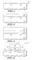
- FIG. 1is a partial cross-sectional view of a semiconductor substrate on which a buffer layer according to one embodiment of the invention has been formed;
- FIG. 2illustrates a processing step subsequent to FIG. 1 in which a gate dielectric layer has been formed
- FIG. 3illustrates a processing step subsequent to FIG. 2 in which a gate electrode layer has been formed over the gate dielectric layer;
- FIG. 4illustrates a processing step subsequent to FIG. 3 in which a transistor has been formed
- FIG. 5illustrates a partial cross-sectional view of a semiconductor substrate on which a gate dielectric according to one embodiment of the invention has been deposited
- FIG. 6illustrates a processing step subsequent to FIG. 5 in which a gate electrode material has been deposited over the gate dielectric layer
- FIG. 7illustrates a processing step subsequent to FIG. 6 in which a transistor has been formed in the semiconductor substrate.
- FIGS. 1 through 4illustrate a method of fabricating a semiconductor device with a dual layer, strontium bearing gate dielectric according to one embodiment of the invention.
- a buffer layer 104is deposited on a first surface 101 of a substrate 102 of a wafer 100 .
- an upper portion of substrate 102 including first surface 101comprises a semiconductor material.
- substrate 102comprises a 100 oriented, single crystal silicon lattice.
- Buffer layer 104may comprise strontium nitride (SrN) formed on upper surface 101 of substrate 102 .
- buffer layer 104may comprise an epitaxial SrN layer.
- the epitaxial SrN layermay be formed with an MBE process in which solid phase strontium is evaporated with a high energy beam to form a vapor phase strontium which is then flowed into a nitrogen bearing chamber in which wafer 100 is located.
- buffer layer 104may be formed by alternative deposition methods including sputtering, chemical vapor deposition (CVD), and atomic layer deposition (ALD).
- CVDchemical vapor deposition
- ALDatomic layer deposition
- a strontium targetis bombarded with high energy particles thereby releasing strontium into a nitrogen containing chamber in which wafer 100 is located.
- the sputtering processmay be a plasma assisted process.
- dielectric layer 106may be formed over buffer layer 104 .
- dielectric layer 106includes strontium, titanium, and oxygen.
- dielectric layer 106may comprise strontium titanate (SrTiO3).
- buffer layer 104comprises epitaxial strontium nitrate
- gate dielectric layer 106typically comprises epitaxial STO formed with a molecular beam epitaxial process.
- dielectric layer 106may be deposited with alternative deposition techniques including sputtering, CVD, and ALD.
- gate dielectric layer 106may include strontium oxynitride (SrON).
- buffer layer 104comprises a first dielectric layer that may include strontium, oxygen, and nitrogen such as strontium oxynitride (SrON) and gate dielectric layer 106 comprises a second dielectric layer that may include strontium nitride.
- the buffer layer 104may include a silicon oxide such as silicon dioxide (SiO2).
- a gate electrode layer 108is formed over dielectric layer 106 .
- the gate electrode layer 108is a conductive material such as a metal or heavily doped polysilicon typically formed with a CVD or sputtering process.
- a thickness of buffer layer 104is in the range of approximately 1 to 5 nanometers
- dielectric layer 106has a thickness in the range of approximately 1 to 10 nanometers
- gate electrode layer 108has a thickness in the range of approximately 100 to 200 nanometers.
- the effective oxide thickness (EOT) of the dielectric stack comprised of dielectric layer 106 and buffer layer 104is preferably less than 3.0 nanometers, where EOT is defined as the thickness of a film divided by its dielectric constant.
- the first plate of a capacitor 107comprises or is integrated with substrate 102 , which is typically made conductive by doping with an implant, diffusion, or other suitable process as is well known in the field of semiconductor fabrication.
- the gate electrode layer 108serves as the second conductive plate and the capacitor dielectric comprises buffer layer 104 and dielectric layer 106 .
- the capacitor 107integrates into a semiconductor fabrication process such that it is formed in conjunction with the formation of a transistor 110 (as depicted and described in greater detail below with respect to FIG. 3 ).
- the first plate of capacitor 107may comprise any conductive film formed above substrate 102 as part of the integrated circuit process.
- a gate electrode 112is formed by patterning and etching gate electrode layer 108 and gate dielectric layer 106 .
- spacer structures 120are formed on sidewalls of gate electrode 112 .
- Source/drain structures 116are formed in an upper portion of substrate 102 proximal to first surface 101 .
- the lateral positioning of gate structure 112 over substrate 102defines a channel region 114 of transistor 110 under gate electrode 212 and source/drain structures 116 are laterally displaced on either side of channel region 114 .
- source/drain regions 116are substantially laterally adjacent to gate electrode 112 .
- source/drain regions 116include an extension diffusion portion 121 formed by performing an extension implant prior to the formation of spacer formations 120 and a heavily doped diffusion portion 118 formed by performing a second source/drain implant after the formation of spacer structures 120 .
- transistor 110includes a substrate 102 , a portion of the substrate proximal to first surface 101 comprising a semiconductor material.
- the transistorincludes the buffer layer 104 and may include the dielectric layer 106 formed over first surface 101 wherein buffer layer 104 may comprise strontium nitride.
- Gate electrode 112is located over the buffer layer 104 and source/drain regions 116 are located in the upper portion of substrate 102 substantially lateral adjacent to gate electrode 112 over a channel 114 .
- a strontium bearing dielectric layer 204is formed over substrate 202 .
- strontium bearing dielectric layer 204is a strontium nitride layer formed with a sputtering, CVD, or ALD deposition process.
- strontium bearing dielectric layer 204includes strontium, oxygen, and nitrogen, such as strontium oxynitride.
- a gate electrode layer 208is deposited over strontium bearing dielectric layer 204 .
- the gate electrode layer 208comprises a conductive material such as a metal or heavily doped polysilicon formed with a CVD or other suitable deposition process.
- the combination of substrate 202 , strontium bearing dielectric layer 204 , and gate electrode layer 208form one embodiment of an integrated circuit capacitor 207 .
- substrate 202comprises a first plate of capacitor 207 and gate electrode layer 208 comprises a second electrode of the capacitor 207 .
- capacitor 207may be formed above substrate 202 by incorporating a strontium dielectric layer between a pair of conductive films.
- FIG. 7further processing of wafer 200 results in the formation of a transistor 210 including a gate electrode 212 formed by appropriate patterning and etching of gate electrode layer 208 and gate dielectric 204 .
- the lateral positioning of gate electrode 212defines a channel region 214 and substrate 202 .
- dielectric spacer structures 220are formed on sidewalls of gate electrode 212 .
- Source/drain structures 216are formed laterally displaced on either side of channel region 214 using an extension implant prior to formation of spacer structures 220 to form extension implant regions 221 and a second implant after the formation of spacer structures 220 to form heavily doped source/drain regions 218 .
Landscapes
- Engineering & Computer Science (AREA)
- Microelectronics & Electronic Packaging (AREA)
- Condensed Matter Physics & Semiconductors (AREA)
- General Physics & Mathematics (AREA)
- Manufacturing & Machinery (AREA)
- Computer Hardware Design (AREA)
- Physics & Mathematics (AREA)
- Power Engineering (AREA)
- Chemical & Material Sciences (AREA)
- Chemical Kinetics & Catalysis (AREA)
- Crystallography & Structural Chemistry (AREA)
- General Chemical & Material Sciences (AREA)
- Insulated Gate Type Field-Effect Transistor (AREA)
Abstract
Description
Claims (8)
Priority Applications (1)
| Application Number | Priority Date | Filing Date | Title |
|---|---|---|---|
| US09/654,704US6518634B1 (en) | 2000-09-01 | 2000-09-01 | Strontium nitride or strontium oxynitride gate dielectric |
Applications Claiming Priority (1)
| Application Number | Priority Date | Filing Date | Title |
|---|---|---|---|
| US09/654,704US6518634B1 (en) | 2000-09-01 | 2000-09-01 | Strontium nitride or strontium oxynitride gate dielectric |
Publications (1)
| Publication Number | Publication Date |
|---|---|
| US6518634B1true US6518634B1 (en) | 2003-02-11 |
Family
ID=24625921
Family Applications (1)
| Application Number | Title | Priority Date | Filing Date |
|---|---|---|---|
| US09/654,704Expired - Fee RelatedUS6518634B1 (en) | 2000-09-01 | 2000-09-01 | Strontium nitride or strontium oxynitride gate dielectric |
Country Status (1)
| Country | Link |
|---|---|
| US (1) | US6518634B1 (en) |
Cited By (32)
| Publication number | Priority date | Publication date | Assignee | Title |
|---|---|---|---|---|
| US20020187578A1 (en)* | 2001-06-12 | 2002-12-12 | Kwon Hong | Method for manufacturing memory device |
| US20030045078A1 (en)* | 2001-08-30 | 2003-03-06 | Micron Technology, Inc. | Highly reliable amorphous high-K gate oxide ZrO2 |
| US20030207032A1 (en)* | 2002-05-02 | 2003-11-06 | Micron Technology, Inc. | Methods, systems, and apparatus for atomic-layer deposition of aluminum oxides in integrated circuits |
| US20040014295A1 (en)* | 2002-07-19 | 2004-01-22 | Hynix Semiconductor Inc. | Atomic layer deposition of titanium nitride using batch type chamber and method for fabricating capacitor by using the same |
| US6696332B2 (en)* | 2001-12-26 | 2004-02-24 | Texas Instruments Incorporated | Bilayer deposition to avoid unwanted interfacial reactions during high K gate dielectric processing |
| US20040067660A1 (en)* | 2002-10-03 | 2004-04-08 | Agere Systems, Inc. | Process for semiconductor device fabrication in which a insulating layer is formed on a semiconductor substrate |
| US20040175882A1 (en)* | 2003-03-04 | 2004-09-09 | Micron Technology, Inc. | Atomic layer deposited dielectric layers |
| US20040183108A1 (en)* | 2001-12-20 | 2004-09-23 | Micron Technology, Inc. | Low-temperature grown high-quality ultra-thin praseodymium gate dielectrics |
| US20040203213A1 (en)* | 2003-03-25 | 2004-10-14 | Yi-Sun Chung | Method for manufacturing an MOS varactor |
| US20050023628A1 (en)* | 2001-01-26 | 2005-02-03 | Yoshihide Senzaki | Multilayer high k dielectric films and method of making the same |
| US20050023624A1 (en)* | 2002-06-05 | 2005-02-03 | Micron Technology, Inc. | Atomic layer-deposited HfAlO3 films for gate dielectrics |
| US20050032292A1 (en)* | 2001-08-30 | 2005-02-10 | Micron Technology, Inc. | Crystalline or amorphous medium-K gate oxides, Y2O3 and Gd2O3 |
| US20050034662A1 (en)* | 2001-03-01 | 2005-02-17 | Micro Technology, Inc. | Methods, systems, and apparatus for uniform chemical-vapor depositions |
| US20060060131A1 (en)* | 2003-12-29 | 2006-03-23 | Translucent, Inc. | Method of forming a rare-earth dielectric layer |
| US20060060826A1 (en)* | 2003-12-29 | 2006-03-23 | Translucent, Inc. | Composition comprising rare-earth dielectric |
| US20060081949A1 (en)* | 2000-12-11 | 2006-04-20 | Jiro Yugami | Semiconductor device and process for producing the same |
| US20060176645A1 (en)* | 2005-02-08 | 2006-08-10 | Micron Technology, Inc. | Atomic layer deposition of Dy doped HfO2 films as gate dielectrics |
| US20060189154A1 (en)* | 2005-02-23 | 2006-08-24 | Micron Technology, Inc. | Atomic layer deposition of Hf3N4/HfO2 films as gate dielectrics |
| US20060228868A1 (en)* | 2005-03-29 | 2006-10-12 | Micron Technology, Inc. | ALD of amorphous lanthanide doped TiOx films |
| US20060261397A1 (en)* | 2003-06-24 | 2006-11-23 | Micron Technology, Inc. | Lanthanide oxide/hafnium oxide dielectric layers |
| US20060289948A1 (en)* | 2005-06-22 | 2006-12-28 | International Business Machines Corporation | Method to control flatband/threshold voltage in high-k metal gated stacks and structures thereof |
| US20070099366A1 (en)* | 2004-08-31 | 2007-05-03 | Micron Technology, Inc. | Lanthanum aluminum oxide dielectric layer |
| US20080096363A1 (en)* | 2005-01-07 | 2008-04-24 | Shrinivas Govindarajan | High Dielectric Constant Materials |
| US20080111186A1 (en)* | 2006-11-14 | 2008-05-15 | Translucent Photonics, Inc. | Field-Effect Transistor Structure and Method Therefor |
| US20080111195A1 (en)* | 2006-11-14 | 2008-05-15 | Translucent Photonics, Inc. | Multi-gate Field Effect Transistor |
| US20080217695A1 (en)* | 2007-03-05 | 2008-09-11 | Translucent Photonics, Inc. | Heterogeneous Semiconductor Substrate |
| US7429515B2 (en) | 2001-12-20 | 2008-09-30 | Micron Technology, Inc. | Low-temperature grown high quality ultra-thin CoTiO3 gate dielectrics |
| US20090008725A1 (en)* | 2007-07-03 | 2009-01-08 | International Business Machines Corporation | Method for deposition of an ultra-thin electropositive metal-containing cap layer |
| US7560793B2 (en) | 2002-05-02 | 2009-07-14 | Micron Technology, Inc. | Atomic layer deposition and conversion |
| US7662729B2 (en) | 2005-04-28 | 2010-02-16 | Micron Technology, Inc. | Atomic layer deposition of a ruthenium layer to a lanthanide oxide dielectric layer |
| US7728626B2 (en) | 2002-07-08 | 2010-06-01 | Micron Technology, Inc. | Memory utilizing oxide nanolaminates |
| US8501563B2 (en) | 2005-07-20 | 2013-08-06 | Micron Technology, Inc. | Devices with nanocrystals and methods of formation |
Citations (1)
| Publication number | Priority date | Publication date | Assignee | Title |
|---|---|---|---|---|
| EP1011149A2 (en)* | 1998-12-16 | 2000-06-21 | Matsushita Electronics Corporation | Semiconductor memory device and method for producing the same |
- 2000
- 2000-09-01USUS09/654,704patent/US6518634B1/ennot_activeExpired - Fee Related
Patent Citations (1)
| Publication number | Priority date | Publication date | Assignee | Title |
|---|---|---|---|---|
| EP1011149A2 (en)* | 1998-12-16 | 2000-06-21 | Matsushita Electronics Corporation | Semiconductor memory device and method for producing the same |
Non-Patent Citations (1)
| Title |
|---|
| Jean Gaude et al.: ":Le systeme strontium-azote. II. Sur une nouvelle combinaison du strontium et de l'azote;" Revue de Chimie Mineral, t. 8, 1971, pp. 287-299; Manuscrit recu le 30 Nov. 1970. |
Cited By (78)
| Publication number | Priority date | Publication date | Assignee | Title |
|---|---|---|---|---|
| US7193281B2 (en)* | 2000-12-11 | 2007-03-20 | Renesas Technology Corp. | Semiconductor device and process for producing the same |
| US20060081949A1 (en)* | 2000-12-11 | 2006-04-20 | Jiro Yugami | Semiconductor device and process for producing the same |
| US20050023628A1 (en)* | 2001-01-26 | 2005-02-03 | Yoshihide Senzaki | Multilayer high k dielectric films and method of making the same |
| US20050087134A1 (en)* | 2001-03-01 | 2005-04-28 | Micron Technology, Inc. | Methods, systems, and apparatus for uniform chemical-vapor depositions |
| US7410668B2 (en) | 2001-03-01 | 2008-08-12 | Micron Technology, Inc. | Methods, systems, and apparatus for uniform chemical-vapor depositions |
| US20050034662A1 (en)* | 2001-03-01 | 2005-02-17 | Micro Technology, Inc. | Methods, systems, and apparatus for uniform chemical-vapor depositions |
| US20020187578A1 (en)* | 2001-06-12 | 2002-12-12 | Kwon Hong | Method for manufacturing memory device |
| US6825129B2 (en)* | 2001-06-12 | 2004-11-30 | Hynix Semiconductor Inc. | Method for manufacturing memory device |
| US8026161B2 (en) | 2001-08-30 | 2011-09-27 | Micron Technology, Inc. | Highly reliable amorphous high-K gate oxide ZrO2 |
| US8652957B2 (en) | 2001-08-30 | 2014-02-18 | Micron Technology, Inc. | High-K gate dielectric oxide |
| US20030045078A1 (en)* | 2001-08-30 | 2003-03-06 | Micron Technology, Inc. | Highly reliable amorphous high-K gate oxide ZrO2 |
| US7208804B2 (en) | 2001-08-30 | 2007-04-24 | Micron Technology, Inc. | Crystalline or amorphous medium-K gate oxides, Y203 and Gd203 |
| US20050032292A1 (en)* | 2001-08-30 | 2005-02-10 | Micron Technology, Inc. | Crystalline or amorphous medium-K gate oxides, Y2O3 and Gd2O3 |
| US20080283940A1 (en)* | 2001-12-20 | 2008-11-20 | Micron Technology, Inc. | LOW-TEMPERATURE GROWN HIGH QUALITY ULTRA-THIN CoTiO3 GATE DIELECTRICS |
| US20040185654A1 (en)* | 2001-12-20 | 2004-09-23 | Micron Technology, Inc. | Low-temperature growth high-quality ultra-thin praseodymium gate dielectrics |
| US7429515B2 (en) | 2001-12-20 | 2008-09-30 | Micron Technology, Inc. | Low-temperature grown high quality ultra-thin CoTiO3 gate dielectrics |
| US20110014767A1 (en)* | 2001-12-20 | 2011-01-20 | Ahn Kie Y | LOW-TEMPERATURE GROWN HIGH QUALITY ULTRA-THIN CoTiO3 GATE DIELECTRICS |
| US20040183108A1 (en)* | 2001-12-20 | 2004-09-23 | Micron Technology, Inc. | Low-temperature grown high-quality ultra-thin praseodymium gate dielectrics |
| US6979855B2 (en) | 2001-12-20 | 2005-12-27 | Micron Technology, Inc. | High-quality praseodymium gate dielectrics |
| US8178413B2 (en) | 2001-12-20 | 2012-05-15 | Micron Technology, Inc. | Low-temperature grown high quality ultra-thin CoTiO3 gate dielectrics |
| US7064058B2 (en) | 2001-12-20 | 2006-06-20 | Micron Technology, Inc. | Low-temperature growth high-quality ultra-thin praseodymium gate dieletrics |
| US7804144B2 (en) | 2001-12-20 | 2010-09-28 | Micron Technology, Inc. | Low-temperature grown high quality ultra-thin CoTiO3 gate dielectrics |
| US6696332B2 (en)* | 2001-12-26 | 2004-02-24 | Texas Instruments Incorporated | Bilayer deposition to avoid unwanted interfacial reactions during high K gate dielectric processing |
| US7160577B2 (en) | 2002-05-02 | 2007-01-09 | Micron Technology, Inc. | Methods for atomic-layer deposition of aluminum oxides in integrated circuits |
| US7670646B2 (en) | 2002-05-02 | 2010-03-02 | Micron Technology, Inc. | Methods for atomic-layer deposition |
| US20030207032A1 (en)* | 2002-05-02 | 2003-11-06 | Micron Technology, Inc. | Methods, systems, and apparatus for atomic-layer deposition of aluminum oxides in integrated circuits |
| US7560793B2 (en) | 2002-05-02 | 2009-07-14 | Micron Technology, Inc. | Atomic layer deposition and conversion |
| US20060000412A1 (en)* | 2002-05-02 | 2006-01-05 | Micron Technology, Inc. | Systems and apparatus for atomic-layer deposition |
| US7589029B2 (en) | 2002-05-02 | 2009-09-15 | Micron Technology, Inc. | Atomic layer deposition and conversion |
| US20050023624A1 (en)* | 2002-06-05 | 2005-02-03 | Micron Technology, Inc. | Atomic layer-deposited HfAlO3 films for gate dielectrics |
| US7554161B2 (en) | 2002-06-05 | 2009-06-30 | Micron Technology, Inc. | HfAlO3 films for gate dielectrics |
| US20100244122A1 (en)* | 2002-07-08 | 2010-09-30 | Leonard Forbes | Memory utilizing oxide nanolaminates |
| US7728626B2 (en) | 2002-07-08 | 2010-06-01 | Micron Technology, Inc. | Memory utilizing oxide nanolaminates |
| US8228725B2 (en) | 2002-07-08 | 2012-07-24 | Micron Technology, Inc. | Memory utilizing oxide nanolaminates |
| US20060040461A1 (en)* | 2002-07-19 | 2006-02-23 | Hynix Semiconductor Inc. | Method of forming a capacitor |
| US20040014295A1 (en)* | 2002-07-19 | 2004-01-22 | Hynix Semiconductor Inc. | Atomic layer deposition of titanium nitride using batch type chamber and method for fabricating capacitor by using the same |
| US7132346B2 (en) | 2002-07-19 | 2006-11-07 | Hynix Semiconductor Inc. | Atomic layer deposition of titanium using batch type chamber and method for fabricating capacitor by using the same |
| US20040067660A1 (en)* | 2002-10-03 | 2004-04-08 | Agere Systems, Inc. | Process for semiconductor device fabrication in which a insulating layer is formed on a semiconductor substrate |
| US20040241947A1 (en)* | 2002-10-03 | 2004-12-02 | Agere Systems, Inc. | Process for semiconductor device fabrication in which a insulating layer is formed on a semiconductor substrate |
| US6770536B2 (en)* | 2002-10-03 | 2004-08-03 | Agere Systems Inc. | Process for semiconductor device fabrication in which a insulating layer is formed on a semiconductor substrate |
| US20060001151A1 (en)* | 2003-03-04 | 2006-01-05 | Micron Technology, Inc. | Atomic layer deposited dielectric layers |
| WO2004079796A3 (en)* | 2003-03-04 | 2005-02-10 | Micron Technology Inc | Atomic layer deposited dielectric layers |
| US20040175882A1 (en)* | 2003-03-04 | 2004-09-09 | Micron Technology, Inc. | Atomic layer deposited dielectric layers |
| US7405454B2 (en) | 2003-03-04 | 2008-07-29 | Micron Technology, Inc. | Electronic apparatus with deposited dielectric layers |
| US7192892B2 (en) | 2003-03-04 | 2007-03-20 | Micron Technology, Inc. | Atomic layer deposited dielectric layers |
| US20040203213A1 (en)* | 2003-03-25 | 2004-10-14 | Yi-Sun Chung | Method for manufacturing an MOS varactor |
| US20060261397A1 (en)* | 2003-06-24 | 2006-11-23 | Micron Technology, Inc. | Lanthanide oxide/hafnium oxide dielectric layers |
| US7655327B2 (en) | 2003-12-29 | 2010-02-02 | Translucent, Inc. | Composition comprising rare-earth dielectric |
| US20060060826A1 (en)* | 2003-12-29 | 2006-03-23 | Translucent, Inc. | Composition comprising rare-earth dielectric |
| US7384481B2 (en) | 2003-12-29 | 2008-06-10 | Translucent Photonics, Inc. | Method of forming a rare-earth dielectric layer |
| US20060060131A1 (en)* | 2003-12-29 | 2006-03-23 | Translucent, Inc. | Method of forming a rare-earth dielectric layer |
| US8237216B2 (en) | 2004-08-31 | 2012-08-07 | Micron Technology, Inc. | Apparatus having a lanthanum-metal oxide semiconductor device |
| US20110037117A1 (en)* | 2004-08-31 | 2011-02-17 | Ahn Kie Y | Lanthanum-metal oxide dielectric apparatus, methods, and systems |
| US7867919B2 (en) | 2004-08-31 | 2011-01-11 | Micron Technology, Inc. | Method of fabricating an apparatus having a lanthanum-metal oxide dielectric layer |
| US20070099366A1 (en)* | 2004-08-31 | 2007-05-03 | Micron Technology, Inc. | Lanthanum aluminum oxide dielectric layer |
| US7863202B2 (en)* | 2005-01-07 | 2011-01-04 | Qimonda Ag | High dielectric constant materials |
| US20080096363A1 (en)* | 2005-01-07 | 2008-04-24 | Shrinivas Govindarajan | High Dielectric Constant Materials |
| US20060176645A1 (en)* | 2005-02-08 | 2006-08-10 | Micron Technology, Inc. | Atomic layer deposition of Dy doped HfO2 films as gate dielectrics |
| US8742515B2 (en) | 2005-02-08 | 2014-06-03 | Micron Technology, Inc. | Memory device having a dielectric containing dysprosium doped hafnium oxide |
| US20090155976A1 (en)* | 2005-02-08 | 2009-06-18 | Micron Technology, Inc. | Atomic layer deposition of dy-doped hfo2 films as gate dielectrics |
| US8481395B2 (en) | 2005-02-08 | 2013-07-09 | Micron Technology, Inc. | Methods of forming a dielectric containing dysprosium doped hafnium oxide |
| US7508648B2 (en) | 2005-02-08 | 2009-03-24 | Micron Technology, Inc. | Atomic layer deposition of Dy doped HfO2 films as gate dielectrics |
| US7989285B2 (en) | 2005-02-08 | 2011-08-02 | Micron Technology, Inc. | Method of forming a film containing dysprosium oxide and hafnium oxide using atomic layer deposition |
| US20060189154A1 (en)* | 2005-02-23 | 2006-08-24 | Micron Technology, Inc. | Atomic layer deposition of Hf3N4/HfO2 films as gate dielectrics |
| US7498247B2 (en) | 2005-02-23 | 2009-03-03 | Micron Technology, Inc. | Atomic layer deposition of Hf3N4/HfO2 films as gate dielectrics |
| US7960803B2 (en) | 2005-02-23 | 2011-06-14 | Micron Technology, Inc. | Electronic device having a hafnium nitride and hafnium oxide film |
| US7365027B2 (en) | 2005-03-29 | 2008-04-29 | Micron Technology, Inc. | ALD of amorphous lanthanide doped TiOx films |
| US20060228868A1 (en)* | 2005-03-29 | 2006-10-12 | Micron Technology, Inc. | ALD of amorphous lanthanide doped TiOx films |
| US7662729B2 (en) | 2005-04-28 | 2010-02-16 | Micron Technology, Inc. | Atomic layer deposition of a ruthenium layer to a lanthanide oxide dielectric layer |
| US20060289948A1 (en)* | 2005-06-22 | 2006-12-28 | International Business Machines Corporation | Method to control flatband/threshold voltage in high-k metal gated stacks and structures thereof |
| US8501563B2 (en) | 2005-07-20 | 2013-08-06 | Micron Technology, Inc. | Devices with nanocrystals and methods of formation |
| US8921914B2 (en) | 2005-07-20 | 2014-12-30 | Micron Technology, Inc. | Devices with nanocrystals and methods of formation |
| US7675117B2 (en) | 2006-11-14 | 2010-03-09 | Translucent, Inc. | Multi-gate field effect transistor |
| US20080111186A1 (en)* | 2006-11-14 | 2008-05-15 | Translucent Photonics, Inc. | Field-Effect Transistor Structure and Method Therefor |
| US20080111195A1 (en)* | 2006-11-14 | 2008-05-15 | Translucent Photonics, Inc. | Multi-gate Field Effect Transistor |
| US20080217695A1 (en)* | 2007-03-05 | 2008-09-11 | Translucent Photonics, Inc. | Heterogeneous Semiconductor Substrate |
| US20090008725A1 (en)* | 2007-07-03 | 2009-01-08 | International Business Machines Corporation | Method for deposition of an ultra-thin electropositive metal-containing cap layer |
| US20090294876A1 (en)* | 2007-07-03 | 2009-12-03 | International Business Machines Corporation | Method for deposition of an ultra-thin electropositive metal-containing cap layer |
Similar Documents
| Publication | Publication Date | Title |
|---|---|---|
| US6518634B1 (en) | Strontium nitride or strontium oxynitride gate dielectric | |
| US9590100B2 (en) | Semiconductor devices containing an epitaxial perovskite/doped strontium titanate structure | |
| US6825506B2 (en) | Field effect transistor and method of fabrication | |
| US7465982B2 (en) | Capacitor structures | |
| US6621114B1 (en) | MOS transistors with high-k dielectric gate insulator for reducing remote scattering | |
| US7714318B2 (en) | Electronic device including a transistor structure having an active region adjacent to a stressor layer | |
| US20050104142A1 (en) | CVD tantalum compounds for FET get electrodes | |
| US6287897B1 (en) | Gate dielectric with self forming diffusion barrier | |
| US8241981B1 (en) | Method of fabricating a deep trench (DT) metal-insulator-metal (MIM) capacitor | |
| US6566205B1 (en) | Method to neutralize fixed charges in high K dielectric | |
| US7504289B2 (en) | Process for forming an electronic device including transistor structures with sidewall spacers | |
| KR20040076798A (en) | Semiconductor device and manufacturing method thereof | |
| US20070001231A1 (en) | Material systems for dielectrics and metal electrodes | |
| US8928051B2 (en) | Metal oxide semiconductor (MOS) device with locally thickened gate oxide | |
| CN107546121B (en) | Semiconductor device and manufacturing method thereof | |
| US6420729B2 (en) | Process to produce ultrathin crystalline silicon nitride on Si (111) for advanced gate dielectrics | |
| JP2010535428A (en) | Method for processing high-k dielectrics for CET scaling | |
| JP3940552B2 (en) | Field effect transistor and manufacturing method thereof | |
| US8969928B2 (en) | Transistors having a control gate and one or more conductive structures | |
| JP2002246591A (en) | Semiconductor device and manufacturing method thereof | |
| JPH05235352A (en) | Semiconductor device and manufacture thereof | |
| KR950004456A (en) | Transistor manufacturing method using arc-shaped sidewall spacer | |
| JPH03280461A (en) | Manufacturing method of semiconductor device |
Legal Events
| Date | Code | Title | Description |
|---|---|---|---|
| AS | Assignment | Owner name:MOTOROLA, INC., ILLINOIS Free format text:ASSIGNMENT OF ASSIGNORS INTEREST;ASSIGNORS:KAUSHIK, VIDYA S.;NGUYEN, BICH-YEN;REEL/FRAME:011853/0905 Effective date:20000828 | |
| AS | Assignment | Owner name:FREESCALE SEMICONDUCTOR, INC., TEXAS Free format text:ASSIGNMENT OF ASSIGNORS INTEREST;ASSIGNOR:MOTOROLA, INC.;REEL/FRAME:015698/0657 Effective date:20040404 Owner name:FREESCALE SEMICONDUCTOR, INC.,TEXAS Free format text:ASSIGNMENT OF ASSIGNORS INTEREST;ASSIGNOR:MOTOROLA, INC.;REEL/FRAME:015698/0657 Effective date:20040404 | |
| FPAY | Fee payment | Year of fee payment:4 | |
| AS | Assignment | Owner name:CITIBANK, N.A. AS COLLATERAL AGENT, NEW YORK Free format text:SECURITY AGREEMENT;ASSIGNORS:FREESCALE SEMICONDUCTOR, INC.;FREESCALE ACQUISITION CORPORATION;FREESCALE ACQUISITION HOLDINGS CORP.;AND OTHERS;REEL/FRAME:018855/0129 Effective date:20061201 Owner name:CITIBANK, N.A. AS COLLATERAL AGENT,NEW YORK Free format text:SECURITY AGREEMENT;ASSIGNORS:FREESCALE SEMICONDUCTOR, INC.;FREESCALE ACQUISITION CORPORATION;FREESCALE ACQUISITION HOLDINGS CORP.;AND OTHERS;REEL/FRAME:018855/0129 Effective date:20061201 | |
| AS | Assignment | Owner name:CITIBANK, N.A., AS COLLATERAL AGENT,NEW YORK Free format text:SECURITY AGREEMENT;ASSIGNOR:FREESCALE SEMICONDUCTOR, INC.;REEL/FRAME:024397/0001 Effective date:20100413 Owner name:CITIBANK, N.A., AS COLLATERAL AGENT, NEW YORK Free format text:SECURITY AGREEMENT;ASSIGNOR:FREESCALE SEMICONDUCTOR, INC.;REEL/FRAME:024397/0001 Effective date:20100413 | |
| FPAY | Fee payment | Year of fee payment:8 | |
| AS | Assignment | Owner name:CITIBANK, N.A., AS NOTES COLLATERAL AGENT, NEW YORK Free format text:SECURITY AGREEMENT;ASSIGNOR:FREESCALE SEMICONDUCTOR, INC.;REEL/FRAME:030633/0424 Effective date:20130521 Owner name:CITIBANK, N.A., AS NOTES COLLATERAL AGENT, NEW YOR Free format text:SECURITY AGREEMENT;ASSIGNOR:FREESCALE SEMICONDUCTOR, INC.;REEL/FRAME:030633/0424 Effective date:20130521 | |
| AS | Assignment | Owner name:CITIBANK, N.A., AS NOTES COLLATERAL AGENT, NEW YORK Free format text:SECURITY AGREEMENT;ASSIGNOR:FREESCALE SEMICONDUCTOR, INC.;REEL/FRAME:031591/0266 Effective date:20131101 Owner name:CITIBANK, N.A., AS NOTES COLLATERAL AGENT, NEW YOR Free format text:SECURITY AGREEMENT;ASSIGNOR:FREESCALE SEMICONDUCTOR, INC.;REEL/FRAME:031591/0266 Effective date:20131101 | |
| REMI | Maintenance fee reminder mailed | ||
| LAPS | Lapse for failure to pay maintenance fees | ||
| STCH | Information on status: patent discontinuation | Free format text:PATENT EXPIRED DUE TO NONPAYMENT OF MAINTENANCE FEES UNDER 37 CFR 1.362 | |
| FP | Lapsed due to failure to pay maintenance fee | Effective date:20150211 | |
| AS | Assignment | Owner name:FREESCALE SEMICONDUCTOR, INC., TEXAS Free format text:PATENT RELEASE;ASSIGNOR:CITIBANK, N.A., AS COLLATERAL AGENT;REEL/FRAME:037356/0143 Effective date:20151207 Owner name:FREESCALE SEMICONDUCTOR, INC., TEXAS Free format text:PATENT RELEASE;ASSIGNOR:CITIBANK, N.A., AS COLLATERAL AGENT;REEL/FRAME:037354/0225 Effective date:20151207 Owner name:FREESCALE SEMICONDUCTOR, INC., TEXAS Free format text:PATENT RELEASE;ASSIGNOR:CITIBANK, N.A., AS COLLATERAL AGENT;REEL/FRAME:037356/0553 Effective date:20151207 | |
| AS | Assignment | Owner name:MORGAN STANLEY SENIOR FUNDING, INC., MARYLAND Free format text:ASSIGNMENT AND ASSUMPTION OF SECURITY INTEREST IN PATENTS;ASSIGNOR:CITIBANK, N.A.;REEL/FRAME:037486/0517 Effective date:20151207 | |
| AS | Assignment | Owner name:MORGAN STANLEY SENIOR FUNDING, INC., MARYLAND Free format text:ASSIGNMENT AND ASSUMPTION OF SECURITY INTEREST IN PATENTS;ASSIGNOR:CITIBANK, N.A.;REEL/FRAME:037518/0292 Effective date:20151207 | |
| AS | Assignment | Owner name:NXP, B.V., F/K/A FREESCALE SEMICONDUCTOR, INC., NETHERLANDS Free format text:RELEASE BY SECURED PARTY;ASSIGNOR:MORGAN STANLEY SENIOR FUNDING, INC.;REEL/FRAME:040925/0001 Effective date:20160912 Owner name:NXP, B.V., F/K/A FREESCALE SEMICONDUCTOR, INC., NE Free format text:RELEASE BY SECURED PARTY;ASSIGNOR:MORGAN STANLEY SENIOR FUNDING, INC.;REEL/FRAME:040925/0001 Effective date:20160912 | |
| AS | Assignment | Owner name:NXP B.V., NETHERLANDS Free format text:RELEASE BY SECURED PARTY;ASSIGNOR:MORGAN STANLEY SENIOR FUNDING, INC.;REEL/FRAME:040928/0001 Effective date:20160622 | |
| AS | Assignment | Owner name:MORGAN STANLEY SENIOR FUNDING, INC., MARYLAND Free format text:CORRECTIVE ASSIGNMENT TO CORRECT THE REMOVE PATENTS 8108266 AND 8062324 AND REPLACE THEM WITH 6108266 AND 8060324 PREVIOUSLY RECORDED ON REEL 037518 FRAME 0292. ASSIGNOR(S) HEREBY CONFIRMS THE ASSIGNMENT AND ASSUMPTION OF SECURITY INTEREST IN PATENTS;ASSIGNOR:CITIBANK, N.A.;REEL/FRAME:041703/0536 Effective date:20151207 | |
| AS | Assignment | Owner name:SHENZHEN XINGUODU TECHNOLOGY CO., LTD., CHINA Free format text:CORRECTIVE ASSIGNMENT TO CORRECT THE TO CORRECT THE APPLICATION NO. FROM 13,883,290 TO 13,833,290 PREVIOUSLY RECORDED ON REEL 041703 FRAME 0536. ASSIGNOR(S) HEREBY CONFIRMS THE THE ASSIGNMENT AND ASSUMPTION OF SECURITYINTEREST IN PATENTS.;ASSIGNOR:MORGAN STANLEY SENIOR FUNDING, INC.;REEL/FRAME:048734/0001 Effective date:20190217 | |
| AS | Assignment | Owner name:MORGAN STANLEY SENIOR FUNDING, INC., MARYLAND Free format text:CORRECTIVE ASSIGNMENT TO CORRECT THE REMOVE APPLICATION11759915 AND REPLACE IT WITH APPLICATION 11759935 PREVIOUSLY RECORDED ON REEL 037486 FRAME 0517. ASSIGNOR(S) HEREBY CONFIRMS THE ASSIGNMENT AND ASSUMPTION OF SECURITYINTEREST IN PATENTS;ASSIGNOR:CITIBANK, N.A.;REEL/FRAME:053547/0421 Effective date:20151207 | |
| AS | Assignment | Owner name:NXP B.V., NETHERLANDS Free format text:CORRECTIVE ASSIGNMENT TO CORRECT THE REMOVEAPPLICATION 11759915 AND REPLACE IT WITH APPLICATION11759935 PREVIOUSLY RECORDED ON REEL 040928 FRAME 0001. ASSIGNOR(S) HEREBY CONFIRMS THE RELEASE OF SECURITYINTEREST;ASSIGNOR:MORGAN STANLEY SENIOR FUNDING, INC.;REEL/FRAME:052915/0001 Effective date:20160622 | |
| AS | Assignment | Owner name:NXP, B.V. F/K/A FREESCALE SEMICONDUCTOR, INC., NETHERLANDS Free format text:CORRECTIVE ASSIGNMENT TO CORRECT THE REMOVEAPPLICATION 11759915 AND REPLACE IT WITH APPLICATION11759935 PREVIOUSLY RECORDED ON REEL 040925 FRAME 0001. ASSIGNOR(S) HEREBY CONFIRMS THE RELEASE OF SECURITYINTEREST;ASSIGNOR:MORGAN STANLEY SENIOR FUNDING, INC.;REEL/FRAME:052917/0001 Effective date:20160912 |