US6517995B1 - Fabrication of finely featured devices by liquid embossing - Google Patents
Fabrication of finely featured devices by liquid embossingDownload PDFInfo
- Publication number
- US6517995B1 US6517995B1US09/525,734US52573400AUS6517995B1US 6517995 B1US6517995 B1US 6517995B1US 52573400 AUS52573400 AUS 52573400AUS 6517995 B1US6517995 B1US 6517995B1
- Authority
- US
- United States
- Prior art keywords
- stamp
- liquid
- layer
- pattern
- substrate
- Prior art date
- Legal status (The legal status is an assumption and is not a legal conclusion. Google has not performed a legal analysis and makes no representation as to the accuracy of the status listed.)
- Expired - Lifetime
Links
Images


Classifications
- H—ELECTRICITY
- H01—ELECTRIC ELEMENTS
- H01L—SEMICONDUCTOR DEVICES NOT COVERED BY CLASS H10
- H01L21/00—Processes or apparatus adapted for the manufacture or treatment of semiconductor or solid state devices or of parts thereof
- H01L21/02—Manufacture or treatment of semiconductor devices or of parts thereof
- H01L21/04—Manufacture or treatment of semiconductor devices or of parts thereof the devices having potential barriers, e.g. a PN junction, depletion layer or carrier concentration layer
- H01L21/18—Manufacture or treatment of semiconductor devices or of parts thereof the devices having potential barriers, e.g. a PN junction, depletion layer or carrier concentration layer the devices having semiconductor bodies comprising elements of Group IV of the Periodic Table or AIIIBV compounds with or without impurities, e.g. doping materials
- H01L21/20—Deposition of semiconductor materials on a substrate, e.g. epitaxial growth solid phase epitaxy
- B—PERFORMING OPERATIONS; TRANSPORTING
- B01—PHYSICAL OR CHEMICAL PROCESSES OR APPARATUS IN GENERAL
- B01J—CHEMICAL OR PHYSICAL PROCESSES, e.g. CATALYSIS OR COLLOID CHEMISTRY; THEIR RELEVANT APPARATUS
- B01J19/00—Chemical, physical or physico-chemical processes in general; Their relevant apparatus
- B01J19/0046—Sequential or parallel reactions, e.g. for the synthesis of polypeptides or polynucleotides; Apparatus and devices for combinatorial chemistry or for making molecular arrays
- B—PERFORMING OPERATIONS; TRANSPORTING
- B82—NANOTECHNOLOGY
- B82Y—SPECIFIC USES OR APPLICATIONS OF NANOSTRUCTURES; MEASUREMENT OR ANALYSIS OF NANOSTRUCTURES; MANUFACTURE OR TREATMENT OF NANOSTRUCTURES
- B82Y10/00—Nanotechnology for information processing, storage or transmission, e.g. quantum computing or single electron logic
- B—PERFORMING OPERATIONS; TRANSPORTING
- B82—NANOTECHNOLOGY
- B82Y—SPECIFIC USES OR APPLICATIONS OF NANOSTRUCTURES; MEASUREMENT OR ANALYSIS OF NANOSTRUCTURES; MANUFACTURE OR TREATMENT OF NANOSTRUCTURES
- B82Y40/00—Manufacture or treatment of nanostructures
- G—PHYSICS
- G03—PHOTOGRAPHY; CINEMATOGRAPHY; ANALOGOUS TECHNIQUES USING WAVES OTHER THAN OPTICAL WAVES; ELECTROGRAPHY; HOLOGRAPHY
- G03F—PHOTOMECHANICAL PRODUCTION OF TEXTURED OR PATTERNED SURFACES, e.g. FOR PRINTING, FOR PROCESSING OF SEMICONDUCTOR DEVICES; MATERIALS THEREFOR; ORIGINALS THEREFOR; APPARATUS SPECIALLY ADAPTED THEREFOR
- G03F7/00—Photomechanical, e.g. photolithographic, production of textured or patterned surfaces, e.g. printing surfaces; Materials therefor, e.g. comprising photoresists; Apparatus specially adapted therefor
- G03F7/0002—Lithographic processes using patterning methods other than those involving the exposure to radiation, e.g. by stamping
- G—PHYSICS
- G03—PHOTOGRAPHY; CINEMATOGRAPHY; ANALOGOUS TECHNIQUES USING WAVES OTHER THAN OPTICAL WAVES; ELECTROGRAPHY; HOLOGRAPHY
- G03F—PHOTOMECHANICAL PRODUCTION OF TEXTURED OR PATTERNED SURFACES, e.g. FOR PRINTING, FOR PROCESSING OF SEMICONDUCTOR DEVICES; MATERIALS THEREFOR; ORIGINALS THEREFOR; APPARATUS SPECIALLY ADAPTED THEREFOR
- G03F7/00—Photomechanical, e.g. photolithographic, production of textured or patterned surfaces, e.g. printing surfaces; Materials therefor, e.g. comprising photoresists; Apparatus specially adapted therefor
- G03F7/0017—Photomechanical, e.g. photolithographic, production of textured or patterned surfaces, e.g. printing surfaces; Materials therefor, e.g. comprising photoresists; Apparatus specially adapted therefor for the production of embossing, cutting or similar devices; for the production of casting means
- H—ELECTRICITY
- H01—ELECTRIC ELEMENTS
- H01L—SEMICONDUCTOR DEVICES NOT COVERED BY CLASS H10
- H01L21/00—Processes or apparatus adapted for the manufacture or treatment of semiconductor or solid state devices or of parts thereof
- H01L21/02—Manufacture or treatment of semiconductor devices or of parts thereof
- H01L21/027—Making masks on semiconductor bodies for further photolithographic processing not provided for in group H01L21/18 or H01L21/34
- H01L21/0271—Making masks on semiconductor bodies for further photolithographic processing not provided for in group H01L21/18 or H01L21/34 comprising organic layers
- H—ELECTRICITY
- H01—ELECTRIC ELEMENTS
- H01L—SEMICONDUCTOR DEVICES NOT COVERED BY CLASS H10
- H01L21/00—Processes or apparatus adapted for the manufacture or treatment of semiconductor or solid state devices or of parts thereof
- H01L21/02—Manufacture or treatment of semiconductor devices or of parts thereof
- H01L21/04—Manufacture or treatment of semiconductor devices or of parts thereof the devices having potential barriers, e.g. a PN junction, depletion layer or carrier concentration layer
- H01L21/18—Manufacture or treatment of semiconductor devices or of parts thereof the devices having potential barriers, e.g. a PN junction, depletion layer or carrier concentration layer the devices having semiconductor bodies comprising elements of Group IV of the Periodic Table or AIIIBV compounds with or without impurities, e.g. doping materials
- H01L21/28—Manufacture of electrodes on semiconductor bodies using processes or apparatus not provided for in groups H01L21/20 - H01L21/268
- H01L21/283—Deposition of conductive or insulating materials for electrodes conducting electric current
- H01L21/288—Deposition of conductive or insulating materials for electrodes conducting electric current from a liquid, e.g. electrolytic deposition
- H—ELECTRICITY
- H01—ELECTRIC ELEMENTS
- H01L—SEMICONDUCTOR DEVICES NOT COVERED BY CLASS H10
- H01L21/00—Processes or apparatus adapted for the manufacture or treatment of semiconductor or solid state devices or of parts thereof
- H01L21/70—Manufacture or treatment of devices consisting of a plurality of solid state components formed in or on a common substrate or of parts thereof; Manufacture of integrated circuit devices or of parts thereof
- H01L21/71—Manufacture of specific parts of devices defined in group H01L21/70
- H01L21/768—Applying interconnections to be used for carrying current between separate components within a device comprising conductors and dielectrics
- H01L21/76801—Applying interconnections to be used for carrying current between separate components within a device comprising conductors and dielectrics characterised by the formation and the after-treatment of the dielectrics, e.g. smoothing
- H01L21/76802—Applying interconnections to be used for carrying current between separate components within a device comprising conductors and dielectrics characterised by the formation and the after-treatment of the dielectrics, e.g. smoothing by forming openings in dielectrics
- H01L21/76817—Applying interconnections to be used for carrying current between separate components within a device comprising conductors and dielectrics characterised by the formation and the after-treatment of the dielectrics, e.g. smoothing by forming openings in dielectrics using printing or stamping techniques
- H—ELECTRICITY
- H10—SEMICONDUCTOR DEVICES; ELECTRIC SOLID-STATE DEVICES NOT OTHERWISE PROVIDED FOR
- H10K—ORGANIC ELECTRIC SOLID-STATE DEVICES
- H10K19/00—Integrated devices, or assemblies of multiple devices, comprising at least one organic element specially adapted for rectifying, amplifying, oscillating or switching, covered by group H10K10/00
- H—ELECTRICITY
- H10—SEMICONDUCTOR DEVICES; ELECTRIC SOLID-STATE DEVICES NOT OTHERWISE PROVIDED FOR
- H10K—ORGANIC ELECTRIC SOLID-STATE DEVICES
- H10K71/00—Manufacture or treatment specially adapted for the organic devices covered by this subclass
- H10K71/10—Deposition of organic active material
- H10K71/12—Deposition of organic active material using liquid deposition, e.g. spin coating
- H10K71/13—Deposition of organic active material using liquid deposition, e.g. spin coating using printing techniques, e.g. ink-jet printing or screen printing
- H—ELECTRICITY
- H10—SEMICONDUCTOR DEVICES; ELECTRIC SOLID-STATE DEVICES NOT OTHERWISE PROVIDED FOR
- H10K—ORGANIC ELECTRIC SOLID-STATE DEVICES
- H10K71/00—Manufacture or treatment specially adapted for the organic devices covered by this subclass
- H10K71/20—Changing the shape of the active layer in the devices, e.g. patterning
- H10K71/231—Changing the shape of the active layer in the devices, e.g. patterning by etching of existing layers
- B—PERFORMING OPERATIONS; TRANSPORTING
- B01—PHYSICAL OR CHEMICAL PROCESSES OR APPARATUS IN GENERAL
- B01J—CHEMICAL OR PHYSICAL PROCESSES, e.g. CATALYSIS OR COLLOID CHEMISTRY; THEIR RELEVANT APPARATUS
- B01J2219/00—Chemical, physical or physico-chemical processes in general; Their relevant apparatus
- B01J2219/00274—Sequential or parallel reactions; Apparatus and devices for combinatorial chemistry or for making arrays; Chemical library technology
- B01J2219/00277—Apparatus
- B01J2219/00351—Means for dispensing and evacuation of reagents
- B01J2219/00382—Stamping
- B—PERFORMING OPERATIONS; TRANSPORTING
- B01—PHYSICAL OR CHEMICAL PROCESSES OR APPARATUS IN GENERAL
- B01J—CHEMICAL OR PHYSICAL PROCESSES, e.g. CATALYSIS OR COLLOID CHEMISTRY; THEIR RELEVANT APPARATUS
- B01J2219/00—Chemical, physical or physico-chemical processes in general; Their relevant apparatus
- B01J2219/00274—Sequential or parallel reactions; Apparatus and devices for combinatorial chemistry or for making arrays; Chemical library technology
- B01J2219/00583—Features relative to the processes being carried out
- B01J2219/00585—Parallel processes
- B—PERFORMING OPERATIONS; TRANSPORTING
- B01—PHYSICAL OR CHEMICAL PROCESSES OR APPARATUS IN GENERAL
- B01J—CHEMICAL OR PHYSICAL PROCESSES, e.g. CATALYSIS OR COLLOID CHEMISTRY; THEIR RELEVANT APPARATUS
- B01J2219/00—Chemical, physical or physico-chemical processes in general; Their relevant apparatus
- B01J2219/00274—Sequential or parallel reactions; Apparatus and devices for combinatorial chemistry or for making arrays; Chemical library technology
- B01J2219/00583—Features relative to the processes being carried out
- B01J2219/00596—Solid-phase processes
- B—PERFORMING OPERATIONS; TRANSPORTING
- B01—PHYSICAL OR CHEMICAL PROCESSES OR APPARATUS IN GENERAL
- B01J—CHEMICAL OR PHYSICAL PROCESSES, e.g. CATALYSIS OR COLLOID CHEMISTRY; THEIR RELEVANT APPARATUS
- B01J2219/00—Chemical, physical or physico-chemical processes in general; Their relevant apparatus
- B01J2219/00274—Sequential or parallel reactions; Apparatus and devices for combinatorial chemistry or for making arrays; Chemical library technology
- B01J2219/00583—Features relative to the processes being carried out
- B01J2219/00603—Making arrays on substantially continuous surfaces
- B01J2219/00605—Making arrays on substantially continuous surfaces the compounds being directly bound or immobilised to solid supports
- B01J2219/00608—DNA chips
- B—PERFORMING OPERATIONS; TRANSPORTING
- B01—PHYSICAL OR CHEMICAL PROCESSES OR APPARATUS IN GENERAL
- B01J—CHEMICAL OR PHYSICAL PROCESSES, e.g. CATALYSIS OR COLLOID CHEMISTRY; THEIR RELEVANT APPARATUS
- B01J2219/00—Chemical, physical or physico-chemical processes in general; Their relevant apparatus
- B01J2219/00274—Sequential or parallel reactions; Apparatus and devices for combinatorial chemistry or for making arrays; Chemical library technology
- B01J2219/00583—Features relative to the processes being carried out
- B01J2219/00603—Making arrays on substantially continuous surfaces
- B01J2219/00605—Making arrays on substantially continuous surfaces the compounds being directly bound or immobilised to solid supports
- B01J2219/0061—The surface being organic
- B—PERFORMING OPERATIONS; TRANSPORTING
- B01—PHYSICAL OR CHEMICAL PROCESSES OR APPARATUS IN GENERAL
- B01J—CHEMICAL OR PHYSICAL PROCESSES, e.g. CATALYSIS OR COLLOID CHEMISTRY; THEIR RELEVANT APPARATUS
- B01J2219/00—Chemical, physical or physico-chemical processes in general; Their relevant apparatus
- B01J2219/00274—Sequential or parallel reactions; Apparatus and devices for combinatorial chemistry or for making arrays; Chemical library technology
- B01J2219/00583—Features relative to the processes being carried out
- B01J2219/00603—Making arrays on substantially continuous surfaces
- B01J2219/00605—Making arrays on substantially continuous surfaces the compounds being directly bound or immobilised to solid supports
- B01J2219/00614—Delimitation of the attachment areas
- B01J2219/00621—Delimitation of the attachment areas by physical means, e.g. trenches, raised areas
- B—PERFORMING OPERATIONS; TRANSPORTING
- B01—PHYSICAL OR CHEMICAL PROCESSES OR APPARATUS IN GENERAL
- B01J—CHEMICAL OR PHYSICAL PROCESSES, e.g. CATALYSIS OR COLLOID CHEMISTRY; THEIR RELEVANT APPARATUS
- B01J2219/00—Chemical, physical or physico-chemical processes in general; Their relevant apparatus
- B01J2219/00274—Sequential or parallel reactions; Apparatus and devices for combinatorial chemistry or for making arrays; Chemical library technology
- B01J2219/00583—Features relative to the processes being carried out
- B01J2219/00603—Making arrays on substantially continuous surfaces
- B01J2219/00605—Making arrays on substantially continuous surfaces the compounds being directly bound or immobilised to solid supports
- B01J2219/00623—Immobilisation or binding
- B01J2219/0063—Other, e.g. van der Waals forces, hydrogen bonding
- B—PERFORMING OPERATIONS; TRANSPORTING
- B01—PHYSICAL OR CHEMICAL PROCESSES OR APPARATUS IN GENERAL
- B01J—CHEMICAL OR PHYSICAL PROCESSES, e.g. CATALYSIS OR COLLOID CHEMISTRY; THEIR RELEVANT APPARATUS
- B01J2219/00—Chemical, physical or physico-chemical processes in general; Their relevant apparatus
- B01J2219/00274—Sequential or parallel reactions; Apparatus and devices for combinatorial chemistry or for making arrays; Chemical library technology
- B01J2219/00583—Features relative to the processes being carried out
- B01J2219/00603—Making arrays on substantially continuous surfaces
- B01J2219/00605—Making arrays on substantially continuous surfaces the compounds being directly bound or immobilised to solid supports
- B01J2219/00632—Introduction of reactive groups to the surface
- B01J2219/00635—Introduction of reactive groups to the surface by reactive plasma treatment
- B—PERFORMING OPERATIONS; TRANSPORTING
- B01—PHYSICAL OR CHEMICAL PROCESSES OR APPARATUS IN GENERAL
- B01J—CHEMICAL OR PHYSICAL PROCESSES, e.g. CATALYSIS OR COLLOID CHEMISTRY; THEIR RELEVANT APPARATUS
- B01J2219/00—Chemical, physical or physico-chemical processes in general; Their relevant apparatus
- B01J2219/00274—Sequential or parallel reactions; Apparatus and devices for combinatorial chemistry or for making arrays; Chemical library technology
- B01J2219/00583—Features relative to the processes being carried out
- B01J2219/00603—Making arrays on substantially continuous surfaces
- B01J2219/00659—Two-dimensional arrays
- B—PERFORMING OPERATIONS; TRANSPORTING
- B01—PHYSICAL OR CHEMICAL PROCESSES OR APPARATUS IN GENERAL
- B01J—CHEMICAL OR PHYSICAL PROCESSES, e.g. CATALYSIS OR COLLOID CHEMISTRY; THEIR RELEVANT APPARATUS
- B01J2219/00—Chemical, physical or physico-chemical processes in general; Their relevant apparatus
- B01J2219/00274—Sequential or parallel reactions; Apparatus and devices for combinatorial chemistry or for making arrays; Chemical library technology
- B01J2219/00718—Type of compounds synthesised
- B01J2219/0072—Organic compounds
- B01J2219/00722—Nucleotides
- B—PERFORMING OPERATIONS; TRANSPORTING
- B01—PHYSICAL OR CHEMICAL PROCESSES OR APPARATUS IN GENERAL
- B01J—CHEMICAL OR PHYSICAL PROCESSES, e.g. CATALYSIS OR COLLOID CHEMISTRY; THEIR RELEVANT APPARATUS
- B01J2219/00—Chemical, physical or physico-chemical processes in general; Their relevant apparatus
- B01J2219/00274—Sequential or parallel reactions; Apparatus and devices for combinatorial chemistry or for making arrays; Chemical library technology
- B01J2219/00718—Type of compounds synthesised
- B01J2219/0072—Organic compounds
- B01J2219/00725—Peptides
- B—PERFORMING OPERATIONS; TRANSPORTING
- B01—PHYSICAL OR CHEMICAL PROCESSES OR APPARATUS IN GENERAL
- B01J—CHEMICAL OR PHYSICAL PROCESSES, e.g. CATALYSIS OR COLLOID CHEMISTRY; THEIR RELEVANT APPARATUS
- B01J2219/00—Chemical, physical or physico-chemical processes in general; Their relevant apparatus
- B01J2219/00274—Sequential or parallel reactions; Apparatus and devices for combinatorial chemistry or for making arrays; Chemical library technology
- B01J2219/00718—Type of compounds synthesised
- B01J2219/0072—Organic compounds
- B01J2219/00731—Saccharides
- C—CHEMISTRY; METALLURGY
- C40—COMBINATORIAL TECHNOLOGY
- C40B—COMBINATORIAL CHEMISTRY; LIBRARIES, e.g. CHEMICAL LIBRARIES
- C40B40/00—Libraries per se, e.g. arrays, mixtures
- C40B40/04—Libraries containing only organic compounds
- C40B40/06—Libraries containing nucleotides or polynucleotides, or derivatives thereof
- C—CHEMISTRY; METALLURGY
- C40—COMBINATORIAL TECHNOLOGY
- C40B—COMBINATORIAL CHEMISTRY; LIBRARIES, e.g. CHEMICAL LIBRARIES
- C40B40/00—Libraries per se, e.g. arrays, mixtures
- C40B40/04—Libraries containing only organic compounds
- C40B40/10—Libraries containing peptides or polypeptides, or derivatives thereof
- C—CHEMISTRY; METALLURGY
- C40—COMBINATORIAL TECHNOLOGY
- C40B—COMBINATORIAL CHEMISTRY; LIBRARIES, e.g. CHEMICAL LIBRARIES
- C40B40/00—Libraries per se, e.g. arrays, mixtures
- C40B40/04—Libraries containing only organic compounds
- C40B40/12—Libraries containing saccharides or polysaccharides, or derivatives thereof
- C—CHEMISTRY; METALLURGY
- C40—COMBINATORIAL TECHNOLOGY
- C40B—COMBINATORIAL CHEMISTRY; LIBRARIES, e.g. CHEMICAL LIBRARIES
- C40B60/00—Apparatus specially adapted for use in combinatorial chemistry or with libraries
- C40B60/14—Apparatus specially adapted for use in combinatorial chemistry or with libraries for creating libraries
- H—ELECTRICITY
- H10—SEMICONDUCTOR DEVICES; ELECTRIC SOLID-STATE DEVICES NOT OTHERWISE PROVIDED FOR
- H10K—ORGANIC ELECTRIC SOLID-STATE DEVICES
- H10K71/00—Manufacture or treatment specially adapted for the organic devices covered by this subclass
- H10K71/821—Patterning of a layer by embossing, e.g. stamping to form trenches in an insulating layer
Definitions
- the present inventionrelates to fabrication of finely featured electronic, chemical, and mechanical devices.
- Electronic and electromechanical componentsare presently fabricated in large, immobile manufacturing facilities that are tremendously expensive to build and operate.
- semiconductor device fabricationgenerally requires specialized microlithography and chemical etching equipment, as well as extensive measures to avoid process contamination.
- the total amount of time required for processing of a single chipmay be measured in days, and typically requires repeated transfer of the chip into and out of vacuum conditions.
- the fabrication processes ordinarily employed to create electronic and electromechanical componentsinvolve harsh conditions such as high temperatures and/or caustic chemicals, limiting the ability to integrate their manufacture with that of functionally related but environmentally sensitive elements.
- the high temperatures used in silicon processingmay prevent three-dimensional fabrication and large-area fabrication; these temperatures are also incompatible with heat-sensitive materials such as organic and biological molecules.
- High temperaturesalso preclude fabrication on substrates such as conventional flexible plastics, which offer widespread availability and low cost.
- U.S. Pat. No. 5,817,550describes a low-temperature roll-to-roll process for creating thin-film transistors on plastic substrates. This approach faces numerous technical hurdles, and does not substantially reduce the large cost and complexity associated with conventional photolithography and etching processes.
- U.S. Pat. No. 5,772,905describes a process called “nanoimprint lithography” that utilizes a silicon mold, which is pressed under high pressure and temperature into a thin film of material. Following cooling with the mold in place, the material accurately retains the features of the mold. The thin film may then be treated to remove the small amount of material remaining in the embossed areas. Thus patterned, the film may be used as a mask for selectively etching underlying layers of functional materials. This process is capable of producing patterns with very fine resolutions at costs significantly below those associated with conventional processes. But it is quite complicated, requiring numerous time-consuming steps to create a single layer of patterned functional material.
- the techniquerequires high application pressures and temperatures at very low ambient pressures, thereby imposing significant complexity with attendant restriction on the types of materials that can be patterned. Perhaps most importantly, this technique is limited to producing single-layer features, thereby significantly limiting its applicability to device fabrication.
- U.S. Pat. No. 5,900,160describes the use of an elastomeric stamp to mold functional materials.
- the stampis deformed so as to print a self-assembled molecular monolayer on a surface.
- MIMICMagnetic Micromolding Against Elastomeric Masters
- MIMICMagnetic Micromolding against Elastomeric Masters
- the techniqueis generally limited to low-resolution features (in excess of 10 ⁇ m), and more importantly, the types of geometries amenable to molding by this technique are limited.
- an object of the present inventionto provide an easily practiced, low-cost process for directly patterning functional materials without the need for multi-stage etching procedures.
- Another object of the inventionis to increase the speed with which layers of functional materials can be patterned.
- Still another object of the inventionis to provide a fabrication process that requires no unusual temperature, pressure, or ambient conditions, thereby increasing the range of materials amenable to patterning.
- a further object of the inventionis to facilitate convenient nanoscale patterning of multiple adjacent layers.
- Yet another object of the inventionis to planarize deposited materials as part of the application process, eliminating the need for additional planarizing processes (such as chemical mechanical polishing), thereby facilitating fabrication of complex three-dimensional devices employing many (e.g., in excess of 100) layers.
- the present inventionutilizes an elastomeric stamp to facilitate direct patterning of electrical, biological, chemical, and mechanical materials.
- a thin film of materialis deposited on a substrate.
- the deposited materialeither originally present as a liquid or subsequently liquefied, is patterned by embossing at low pressure using an elastomeric stamp having a raised pattern.
- the patterned liquidis then cured to form a functional layer.
- the deposition, embossing, and curing stepsmay be repeated numerous times with the same or different liquids, and in two or three dimensions.
- the various deposited layersmay, for example, have varying electrical characteristics, interacting so as to produce an integrated electronic component.
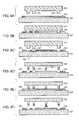
- FIGS. 1A-1Dare greatly enlarged sectional views illustrating fabrication of an elastomeric stamp in accordance with the present invention
- FIGS. 2A and 2Bare side elevations illustrating application of a thin, uniform film of liquid onto a substrate
- FIGS. 3A-3C and 3 D- 3 Fare sectional views illustrating, respectively, the embossing process of the present invention as applied to planar surfaces and non-planar surfaces;
- FIGS. 3G-3Iare sectional views illustrating planarization and the creation of vias using the present invention.
- FIGS. 4A-4Fare sectional views illustrating fabrication of an electronic inverter in accordance with the present invention.
- FIGS. 5A-5Fare plan views of the structures shown sectionally in FIGS. 4A-4F;
- FIGS. 6A-6Gare sectional views illustrating fabrication of a microelectromechanical device in accordance with the present invention.
- FIGS. 7A-7Gare plan views of the structures shown sectionally in FIGS. 6A-6G;
- FIGS. 8A-8Fare sectional views illustrating fabrication of a biochip in accordance with the present invention.
- FIGS. 9A-9Cschematically illustrate, respectively, a single SRAM circuit, a two-dimensional array of such circuits, and a three-dimensional array of such circuits;
- FIGS. 10A and 10Bare sectional views illustrating fabrication of a field-mission display device in accordance with the present invention.
- FIG. 11is a block diagram of a preferred nano-embossing system implementing the present invention.
- FIGS. 12A and 12Bschematically illustrate alternative configurations for synthesizing nanoparticles.
- FIGS. 1A-1Dillustrate an exemplary approach to fabricating an elastomeric stamp useful in the practice of the present invention.
- a substrate 100is patterned with a series of recessed features 105 and projecting features 110 . These features correspond in size and arrangement (but not in depth) to the pattern ultimately desired for a component layer. Accordingly, the features 105 , 110 may be inscribed using conventional techniques such as photolithography, e-beam, focused ion-beam, micromachining, or other lithographic approaches. Feature sizes as small as 150 nm have been accurately obtained and utilized, although even smaller features are of course possible.
- Substrate 100may, for example, be any surface sufficient smoothness that may be conveniently patterned, and which will not bond to the material from which the stamp is to be formed. Suitable materials include, for example, silicon, metal wafers, and exposed photoresist.
- a raised enclosure 115is applied to substrate 100 so as to surround the pattern of features 105 , 110 .
- Enclosure 115may be, for example, a metal or plastic wall, the outer contour of which is designed to fit within the device that will apply the stamp as hereinbelow described.
- An uncured elastomer 120 in liquid formis poured into the well 125 formed by enclosure 115 and features 105 , 110 .
- elastomer 120is a curable rubber or silicone material such as polydimethylsiloxane (PDMS), e.g., the SYLGARD-184 material supplied by Dow Corning Co.
- PDMSpolydimethylsiloxane
- enclosure 115is desirably held against the surface of substrate 100 with a modest pressure or set within a conforming groove in substrate 100 .
- a sufficient amount of elastomer 120is poured into well 125 to completely fill features 105 and to provide a stable body mass for stamping operations.
- the elastomer 120is then cured into a solid plug 130 .
- the PDMS material mentioned abovemay be cured by heating in an oven at 80° C. for 2 h.
- Other silicone elastomersmay be cured by exposure to moisture, e-beam or actinic (e.g., ultraviolet) radiation, or by addition of a cross-linking agent.
- the solid plug 130is separated, with or without enclosure 115 , from substrate 100 as shown in FIG. 1D to form a finished stamp 132 .
- the underside of plug 130has a series of projecting and recessed features 135 , 140 complementary to the features 105 , 110 of substrate 100 , which are left undamaged by the foregoing process steps; moreover, little if any elastomer is desirably left on the substrate 100 when plug 130 is removed.
- Enclosure 115may be removed along with plug 130 as shown in FIG. 1D, or it may instead be left in place on substrate 100 . If it is removed and its association with plug 130 retained, it may serve several purposes: facilitating mechanical attachment to the stamping device, assisting with alignment of the stamp (for example, enclosure 115 may have an alignment tab that mates with a complementary recess in the stamping device), and limiting lateral deformation of plug 130 . To further limit lateral deformation, plug 130 may be made relatively thin (by pouring the liquid elastomer 120 to a level not substantially above the surface of substrate 100 ) and capped by a solid support structure. A fenestrated film or other rigidity-conferring filler material may be added to liquid elastomer 120 prior to curing, thereby integrating within the resulting polymer matrix to further enhance the rigidity of plug 130 .
- a stampmay be patterned by selectively curing a thin film of the elastomer by exposure to actinic radiation through a mask followed by photochemical development (to remove the exposed or the unexposed areas), or by selective thermal curing with an atomic force microscope (AFM) thermal tip.
- the stamp 132may also be fabricated from non-elastomeric stiff materials for better control of deformation.
- the procedures described abovecan be carried out with a polyacrylate rather than an elastomer. Suitable polyacrylates include polyfunctional acrylates or mixtures of monofunctional and polyfunctional acrylate that may be cured by e-beam or ultraviolet (UV) radiation.
- the stamp 132may be cleaned by coating the patterned surface with a liquid polyimide such as Japanese Synthetic Rubber, curing the polyimide in place, and then peeling it off the stamp. This process will remove dust and debris without harming the patterned stamp surface.
- a liquid polyimidesuch as Japanese Synthetic Rubber
- the stampis applied to a liquid which, when cured, provides a desired electrical, chemical, biological, and/or mechanical functionality.
- the liquidmay be a colloidal dispersion of nanoparticles or carbon nanotubes; an uncured polyimide; a solution of biological material; or a solution of a suitable sacrificial or release layer which may later be dry- or wet-etched (e.g., PMMA).
- the liquidis present on a substrate (or on a previously deposited and cured layer) as a thin, uniform film.
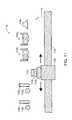
- a deposited liquidcan be drawn into such a film by various techniques, one of which is illustrated in FIGS. 2A and 2B.
- a substrate 200which may be a glass slide, a silicon wafer, a sheet of plastic, or other smooth material—receives a bead 210 of liquid.
- a smooth rod 220(which may be glass or a flexible material) is dragged across substrate 200 in the direction of the arrow, drawing the bead 210 into a uniform film 230 .
- the pressure between rod 220 and substrate 200can vary without affecting the resultant thickness of film 230 ; indeed, rod 220 can even be held slightly above substrate 200 (so that no contact is actually made).
- the speed with which rod 220 is drawn across substrate 200does affect the thickness of film 230 , however, with faster travel resulting in a thinner film. Accordingly, for a film of uniform thickness, rod 220 should be drawn at a constant speed, and should not be allowed to rotate as it is drawn.
- the film thicknessis also affected by the size (diameter) of rod 220 .
- the film 230will typically still be in a liquid state. Depending on the liquids substantial loss of volume may occur by evaporation; indeed, a loss of 90% of the initial height of the film is not unusual. Thus, a thin film of liquid initially 100 ⁇ 10 nm in height may dry down to a film 10 ⁇ 1 nm in height. We have routinely obtained dry films with heights less than 40 nm using this technique.
- a rod to produce a thin filmis not an option.
- the materialmay not wet to the surface of substrate 200 , or the solvent may evaporate almost instantly.
- An alternative application technique useful in such casesutilizes a stamp having a patterned surface as described above. A small line of the liquid material to be drawn into a film is deposited onto substrate 200 . One edge of the stamp is brought into contact with substrate 200 immediately next to the line of liquid. The stamp is then lowered into contact with the substrate, displacing the liquid in front of it and producing a thin, patterned layer of material under the stamp.
- Another alternativeinvolves application of the material to be patterned as a droplet, either to the surface of the receiver substrate or to the raised-pattern surface of the stamp.
- the stampis then brought into contact with the substrate surface, thereby molding the applied material in the pattern of the stamp.
- the materialmay be cured (e.g., thermally) with the stamp in contact with the substrate.
- this approachhas been applied to liquid-phase polyimide, vinyl, and nanoparticle metal inks, which are cured by activating a hotplate underlying the substrate following patterning. It is found, however, that this approach is most useful for insulators (such as polymers) because the resulting patterned film is contiguous.
- the processalso works best with viscous materials that exhibit limited outgassing during cure (although PDMS stamps are to some degree porous to may outgassing components).
- FIGS. 3A-3Cillustrate the embossing technique of the present invention as applied to a planar surface.
- a substrate 300is coated with a thin, uniform film 305 of liquid as described above.
- An elastomeric stamp 310 having a pattern of projecting and recessed features 315 , 320is lowered until the projecting features 315 make contact with substrate 300 , thereby displacing liquid 305 at the regions of contact.
- the height (or heights) of the recessed features 320exceeds that of the liquid that will be displaced therein.
- the area dimensions of projecting features 315are constrained by the need for these features to push aside the liquid 305 and either make contact with substrate 300 or at least displace enough liquid to facilitate its convenient subsequent removal.
- the maximum areas of features 315depend greatly on the viscosity of the liquid, the thickness of the film 305 , and the nature of the stamp elastomer.
- metallic nanoparticles in suspension15%) with a wet film thickness of 500 nm, it has been found that an elastomeric stamp formed from PDMS can completely transport the nanoparticle-containing liquid over a distance greater than 5 ⁇ m.
- thesemay have convex, rather than flat, surfaces; for example, the features may be domed, peaked, or otherwise shaped to make contact with substrate 300 at a small region, progressively moving more liquid as stamp 310 is pressed against substrate 300 and the features 315 flatten.
- Stamp 310is preferably lowered onto substrate 300 using a slight rocking motion. Since the stamp is elastomeric, it may be slightly flexed so that one edge first makes contact with the substrate before the rest of the stamp rolls into place. This approach prevents or reduces the formation of air bubbles. No unusual pressure, temperature, or ambient conditions are necessary for the embossing process. Very light or no pressure is applied to the stamp 310 so the projecting features 315 penetrate the liquid film 305 . Any attractive force between projecting features 315 and substrate 300 will assist with the transport of liquid into recesses 320 , and may also allow pressure to be removed—so that features 315 merely rest against substrate 300 —without sacrificing contact.
- stamp 310With the stamp 310 against substrate 300 as shown in FIG. 3B, the film 305 may be partially or completely cured.
- the curing modeis dictated by the nature of the liquid, and may include one or more process steps such as heating, evaporating a solvent (to which the elastomer of stamp 310 is permeable), UV exposure, laser annealing, etc.
- Stamp 310is removed from substrate 300 as shown in FIG. 3C, leaving a pattern of fully or partially cured film traces 325 that correspond to the pattern of recesses 320 .
- stamp 310is removed using a rocking motion. Smooth, uniform motion improves the quality of the pattern 325 and prevents damage thereto from minuscule bursts of air.
- stamp 310may be immediately reused without cleaning.
- the patterned liquid 325may at this point be cured into full solidity.
- the absence of the stamp 310facilitates such additional mechanisms as vacuum evaporation and chemical modification (e.g., by addition of a cross-linker).
- the film patterned by the stamp 310may begin as a solid rather than a liquid.
- the filmmay be heated to decrease viscosity before stamp 310 is brought into contact therewith.
- stamp 310may itself be heated to a temperature sufficient to melt the solid film upon contact.
- FIG. 3Dshows a substrate 300 having a previously patterned layer of a first material 330 .
- a thin film 335 of liquidis drawn over material 330 and, where exposed, substrate 300 ; the liquid 335 is generally conformal, resulting in an uneven liquid surface. Maintaining precise alignment among patterned layers is obviously vital to proper functioning of the finished device.
- stamp 340is well-suited to patterning such an uneven surface while maintaining precise rendition of the stamp pattern. As shown in FIG. 3E, stamp 340 is lowered as discussed previously. Because of its elastic character, stamp 340 deforms to allow different projecting features 345 to reach solid surfaces of different heights without substantial lateral deflection. As a result, the pattern 350 of material 335 that remains upon removal of stamp 340 is substantially complementary to the pattern of projecting features 345 , notwithstanding the different heights of the embossed regions. Naturally, the degree of fidelity to the stamp pattern depends on the degree of elasticity inherent in the stamp and the differences in height that must be accommodated.
- the embossed pattern of material 350is cured.
- the curing mode chosenmust not damage the previously cured layer 330 .
- a thin film of depositedmay be conformal, resulting in a surface of varying heights (rather than filling recesses to create a planar surface).
- the embossing technique of the present inventioncan be used not only to planarize such deposited layers, but also to create “vias” that interconnect layers not directly in contact with each other.
- a substrate 300is patterned with a previously deposited and embossed layer of a first material 360 .
- a thin film 365 of liquidis drawn over material 360 and, where exposed, substrate 300 ; once again the liquid 365 is generally conformal, resulting in an uneven liquid surface.
- it is desirable for the component layer formed from liquid 365to be planar rather than conformal.
- planarizationis essential for microelectromechanical (MEM) structures and many-layer three-dimensional circuits.
- the present inventioncan accomplish both planarization and the creation of vias among non-adjacent stratified layers.
- the projecting features of a stamp 370(representatively indicated at 375 ) have elevations chosen such that, with the surfaces 377 of the projections in contact with substrate 373 , the recessed portions of stamp 370 (representatively indicated at 380 ) make contact with the surface of liquid 365 .
- the resultis planarization of the liquid layer 365 where it is in contact with stamp surfaces 380 .
- stamp 370is removed (FIG. 31 )
- that layersubstantially planar with the exception of edge ridges shown at 385 .
- a via 390is established between the surface of substrate 300 and the top surface of layer 365 .
- a layer subsequently deposited on layer 365therefore, can make contact with substrate 300 , and this subsequently deposited layer can also be planarized in the manner just described.
- the via 390can be made to persist through multiple layers by embossing with a similar projecting feature as each such layer is applied. In this way, contact between distant layers may be effectuated.
- Liquid 365may or may not be cured (totally or partially) before stamp 370 is withdrawn in the manner hereinabove described. Following curing, the liquid 365 may decrease in height, jeopardizing planarity. This problem can be overcome by applying additional layers of the same material and embossing with the same pattern of features 377 , 380 . The ability to planarize and pattern in the same step represents a significant fabrication capability and improvement over the prior art.
- An alternative arrangementutilizes a device which, under computer control, is capable of changing its surface topology in accordance with a desired pattern and then acting as a stamp.
- a devicewhich, under computer control, is capable of changing its surface topology in accordance with a desired pattern and then acting as a stamp.
- Such a devicemay be built, for example, using an array of MEM elements that are actuated electrostatically, thermally, magnetically, piezoelectrically or by other computer-controllable means, actuation of an element causing it to alter the degree or manner in which it projects from the surface of the array.
- micro-mirror arrayin which an array of elements is caused to tilt either out of plane or lie flat depending on an electrical signal (see Kim et al., Society for Information Display 99 Digest , p. 982 (1999)).
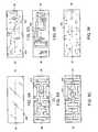
- FIGS. 4A-4F and 5 A- 5 Fillustrate fabrication of a two-transistor electronic inverter
- FIGS. 4A-4Fare a section taken from the corresponding one of FIGS. 5A-5F along the line labeled with the figure number.
- Functional layersare built up on a substrate 400 (FIGS. 4A, 5 A), which may be, for example, a glass slide, a plastic sheet, a silicon wafer, or any other material having a sufficiently smooth surface 400 s. Each added layer is patterned by a different stamp.
- a patterned conductive metal layer 410is established on surface 400 s of substrate 400 .
- a metal-containing liquidsuch as a suspension of gold or silver nanoparticles in a suitable carrier liquid
- the applied liquidis patterned with a stamp as described above so as to create a series of channels that reveal the surface 400 s of substrate 400 .
- the liquidis then cured (e.g., in the case of a metal nanoparticle suspension, the carrier is evaporated so that the metal particles coalesce into a substantially continuous, conductive patterned film).
- the pattern formedincludes a pair of transistor gaps 412 , a ground rail 414 , and a V cc rail 416 .
- a semiconductive layer 420is deposited onto the conductive layer 410 .
- Layer 420completely fills and is planarized over the channels 412 , so that in these locations, layer 420 is in contact with substrate 400 . Otherwise, the pattern of layer 420 substantially matches that of layer 410 so that the semiconductor 420 does not bridge between metal lines.
- layer 420is removed by the embossing process to reveal the underlying layer 410 , while in other areas 424 overlying channels previously defined through layer 410 , substrate 400 is revealed.
- Semiconductive layer 420may be applied as a liquid suspension of semiconductor (e.g., silicon, germanium, CdSe, etc.) nanoparticles as described, for example, in U.S. Pat. No. 5,534,056 (the entire disclosure of which is hereby incorporated by reference). Again, following patterning, the layer may be cured by evaporating the carrier so as to coalesce the particles into a continuous patterned film.
- An insulating layer 430is applied over semiconductive layer 420 as shown in FIGS. 4D, 5 D.
- Layer 430completely fills the vias 424 , and is planarized thereover.
- a via 432slightly smaller in diameter than the via 422 (see FIG. 4C) created earlier, is formed through that via 422 to reveal layer 410 .
- the insulating layermay be applied as an uncross-linked liquid polymer precursor, such as a radiation-cure coating (polyacrylates and polymethacrylates, for example, are suitable for this purpose). Following patterning and removal of the stamp, the polymer precursor may be cured (i.e., cross-linked) into solidity by exposure to UV or e-beam radiation.
- a second metal layer 435is applied to insulating layer 430 and patterned by stamping.
- a plug of the metal layer 435completely fills the via 432 created previously and connects to metal layer 410 ; because via 432 has a smaller diameter than via 424 , a layer of insulating material separates the plug of metal from semiconductor layer 420 within the via 432 .
- the second metal layer 430forms the gates 440 of the two transistors.
- An encapsulant 450such as a UV-cured polymer, epoxy or spin-on glass is applied as a coating over layer 435 to protect all underlying functional layers from contamination or physical damage.
- the encapsulantwhich is applied at a sufficient thickness to fill all exposed channels, also adds structural rigidity to the finished device.
- FIGS. 6A-6G and 7 A- 7 Gillustrate fabrication of a freely rotating MEM wheel.
- Each of FIGS. 6A-6Gis a section taken from the corresponding one of FIGS. 7A-7G along the line labeled with the figure number.
- the structureincludes a first sacrificial or release layer, a second sacrificial or release layer, a first metal layer, a third sacrificial or release layer, and a second metal layer. After all layers are applied, a final release step etches away the release layers to liberate a purely metallic structure. Each layer is patterned using an elastomeric stamp as described above.
- a substrate 600(FIGS. 6A, 7 A), which may be a glass slide, a plastic sheet, a silcion wafer, or any other appropriately smooth surface (for MEM applications a relatively stiff substrate may be desirable), receives a first release layer 610 as shown in FIGS. 6B, 6 C.
- Release layer 610may be, for example, a polymer (such as PMMA) soluble or wet-etchable in a solvent (such as acetone), or etchable by dry-etch techniques (such as plasma etching); or may be a spin-on glass etchable in hydrofluoric acid.
- Release layer 610completely covers substrate 600 with the exception of a hole 612 patterned in the release layer by means of the elastomeric stamp. This hole 612 will receive material for the axle of the wheel.
- the second release layer 620is patterned as shown in FIGS. 6C, 7 C.
- the patternincludes a series of depressions 622 . These will be filled with metal to create dimples on the rotating wheel.
- the hole 612is patterned in the center of layer 620 .
- the first metal layer 630fills the holes 612 , 622 (see FIG. 6C) patterned in the first two release layers 610 , 620 .
- Layer 630is planarized over these holes. Stamping eliminates metal from a pair of concentric circular regions 632 , 635 . Region 632 defines the edge of the wheel, and region 635 faciliatates separation of the wheel from the axle. The bottom of the wheel fills the depressions 622 (FIGS. 6C, 7 C), forming dimples that will reduce stiction between the wheel and substrate 600 . Not shown are small holes patterned in the wheel to allow etchant to reach the underlying release layers 610 , 620 .
- the third release layer 640is added and patterned as shown in FIGS. 6E, 7 E.
- This layeruses a stamp identical to that employed to pattern the first release layer 610 , forming a hole 645 in the center for the axle of the wheel.
- the second metal layer 650(FIGS. 6F, 7 F) is patterned to create a cap 652 on the axle of the wheel. This cap prevents the wheel from leaving the axle after all release layers are etched away.
- Metal layer 650is also crosshatched to create small islands 655 of metal. These islands represent excess material and will be removed when the release layers are etched away, but are included to facilitate separation of the release layers. During the release step it may be necessary to use a supercritical CO 2 release to avoid suckdown problems between the wheel and the substrate.
- the finished deviceis a wheel 660 with dimples 662 on its bottom surface, an axle 665 about which the wheel 660 is free to rotate, and a cap 650 that holds the wheel 660 in place on the axle 665 .
- MEM structures amenable to production using the present inventioninclude, for example, so-called heatuators, linear comb drives, and combustion engines.
- FIGS. 8A-8Fillustrate use of the present invention to create a so-called “biochip,” i.e., an electronically active or readable substrate having a dense array of different biological materials (e.g., DNA probes, protein probes, carbohydrates).
- a chipcan be used, for example, to identify samples of interest or to test for the presence of various molecular sequences. See, e.g., U.S. Pat. Nos. 5,605,662, 5,874,219, 5,744,305 and 5,837,832. If a sufficiently large array of different oligonucleotides can be deposited onto a surface, then one may in principle obtain full genome sequence information via the method of sequencing by hybridization (Skiena et al., Proc.
- an elastomeric stamp 810has a series of projecting features 815 .
- a substrate 820has deposited thereon a thin film of biological material 822 .
- Stamp 810is lowerd until projecting features 815 penetrate and displace the liquid film 812 to make contact with the underlying substrate 820 (FIG. 8 B). The stamp 810 is then removed from contact with the substrate 810 , leaving a pattern 825 of biological material and a complementary pattern of regions 827 from which biological material has been removed (FIG. 8 C).
- FIG. 8Dshows a second substrate 830 having an array of projecting features 832 each with a biological receptor 835 bonded thereto.
- This biological receptoruniquely bonds to constituents of the biological material 822 ; for example, biological material 822 may be a protein solution, and the receptor 835 an antibody specific for the protein.
- the second substrate 830is aligned above the original substrate 820 .
- the second substrate 830is brought into contact with substrate 820 (FIG. 8 E); some of the projecting features 832 overlie biological material 825 , while others overlie voids 827 .
- Biological materialbinds to receptors attached to projecting features that penetrate the liquid, while projecting features brought into contact with (or proximity to) void areas 827 remain unmodified.
- FIG. 8Fshows the second substrate 830 removed from contact with substrate 820 .
- Biological material on the original substratewas selectively transferred to certain projecting features 832 of the second substrate 830 and not to others; the second substrate 830 , thus selectively patterned (with features 832 on the order of 10 nm-100 82 m) and chemically reacted, may serve as a biochip.
- the liquid material remaining on the original substrate 820may be used to produce additional biochips.
- the biochipmay be brought into contact with a third substrate having a different biological material, and which has been patterned with the original stamp 810 or with a different stamp. In this way, a second layer of biological material can be selectively added to various of of the projecting features 832 .
- a biological resist layeris patterned by an elastomeric stamp in accordance with the invention, and is then brought into contact with a substrate having projecting features.
- the resist materialbinds selected projecting features based on the respective patterns of the features and the resist.
- the entire structureis then immersed in a functional biological material, which binds only to projecting features that have not received resist.
- the structureis immersed in an etch bath that removes the resist material (and any biological material that may have bound to it), but leaving undisturbed biological material bound to features that did not receive resist.
- biological materialmay be directly transferred from the projecting features of the elastomeric stamp onto selected sites (e.g., raised features) on the substrate. Areas of the stamp corresponding to recessed features do not transfer material. In this fashion the substrate may be patterned without the need for an intermediate transfer step. Spreading of the transferred material is avoided by maintaining only a very thin film of material in the plate from which the stamp is “inked.” It is important, of course, that the receiver surface exhibit a higher affinity for the biological material than the stamp. PDMS has a very low surface energy, making it ideal for transferring a wide range of materials.
- a metal nanoparticle dispersionmay be applied as a thin film to a flat surface such as glass or plastic.
- a patterned elastomeric stampis brought into contact with the film of material and withdrawn, and the material adhering to the stamp transferred to a second surface.
- conducting structureswith edge resolutions on the order of 300 nm.
- Each new nucleotide in the sequenceis first blocked by reaction with 4′,4′dimethoxytrityl (DMT) and then combined with a highly reactive methylated diisopropyl phosphoramidite group, which links the nucleotide with the one previously added.
- the blocking groupis removed by detritylation, which renders the newly linked nucleotide available for linkage to a further nucleotide.
- all methyl groupsare removed by exposure to alkaline pH.
- carbohydrate-assembly machinesby employing the standard chemistries used in protein-assembly machines (e.g., repeated sequences of chemically blocking an amino acid, activation, linkage to the most recently added amino acid, followed by unblocking), carbohydrate-assembly machines, protein or carbohydrate biochips may be fabricated.
- biochipsit may be desirable to have good separation between biological domains (such as between oligonucleotides of different sequence). This may be accomplished by stamping such sequences onto a non-planar or porous surface.
- the term “porous”refers to non-planar features that physically separate unique nucleotide sequences (or other chemically distinct biomolecules).
- each sequencemay be patterned on the top surface of a raised pillar, each of which is physically separated from its neighbors. This design allows for convenient removal unwanted chemistries, since these can be continuously withdrawn as they accumulate at the bases of the pillars.
- each nucleotide sequencemay be deposited into a separate recessed well.
- FIG. 9Aschematically illustrates a single SRAM 900 circuit with a power rail V cc 910 and a ground rail 915 .
- the SRAM 900is addressed using a horizontal control line 920 and a vertical control line 925 which, when both high, activate the split-gate transistor structure 930 and connect the read/write line 935 to the memory cell.
- the volatile memoryis stored in a pair of cross-coupled inverters 940 .
- This circuitcan be fabricated using the embossing technique with five different elastomeric stamps: two metal layers, a semiconducting layer, a thin insulating layer, and a planarizing layer with vias.
- FIG. 9Bshows the manner in which the basic circuit 900 can be utilized as a “tile” in a two-dimensional array of such circuits.
- the circuit 900is replicated 16 times in a contiguous, 4 ⁇ 4 two-dimensional array 950 .
- This memory array 950has power and ground rails, the horizontal control lines running along the left and right edges 955 , and the vertical control lines and read/write lines running along the top and bottom edges.
- the array 950is produced by applying, in the pattern of the array, the same five stamps over each applied layer. The stamped regions interact to form the continuous circuit 950 .
- the arraycan be extended into three dimensions by replicating the two-dimensional array 950 in a vertical stack 970 .
- a memory addressis divided so that the first bits of the address decode into a set of horizontal control lines that all lie in the same two-dimensional position but are stacked vertically, and the last bits of the address decode the vertical control lines in the same way.
- a word of memoryis stored in the same two-dimensional position of different arrays in the vertical stack (so that the number of bits in a word of data corresponds to the number of vertically stacked memory arrays).
- the decoding circuitry on the edges of the memorymay also be produced using the same five masks repeated for each layer with vias interconnecting the layers.
- cellular automataare interconnected processing cells that interact with neighbors to compute in parallel.
- Cellular automataare often used to simulate three-dimensional environments, but conventional approaches are inherently two-dimensional and therefore limited in processing capacity. By creating circuits in three dimensions with many layers, it is possible to overcome this scaling limitation.
- a cellularautomata devicewould include many two-dimensional arrays of cells stacked vertically to create an interconnected three-dimensional array.
- Three-dimensional devices amenable to fabrication in accordance with the present inventionis a neuronal structure consisting of many individual electronic “neurons” (each represented by a processor) arranged in three-dimensions with many “dendritic” interconnects between neighboring devices. Each neuron is affected by all of its surrounding neurons and in turns affects the neurons to which it is connected. Neural networks created in three-dimensions avoid many of the scaling problems that plague today's two-dimensional circuits.
- Another application of the stamping process of the present inventioninvolves creation of electron-emission structures for use in field-emission displays (FEDs).
- FEDsfield-emission displays
- Today, these devicesare typically fabricated in silicon and are quite expensive and complicated to produce; the most common structure used is a Spindt-tip.
- Recently, researchhas shown that by using materials with a lower work function (e.g., single-wall carbon nanotubes), much simpler structures can be fabricated with equal or better efficiency than typical silicon emitters (Choi et.al., Society for Information Display 99 Digest , p. 1134 (1999)).
- the growth temperatures for producing nanotubesare well above the melting point for glass or plastic substractes (exceeding 800° C.) and have thus not been integrated with processes employing such substrates.
- a slurry of metallic (preferably gold) nanoparticles and chopped up nanotubes (nanopipes)is dissolved in a solvent.
- this slurryis then patterned, by stamping, onto a substrate 1010 (e.g., a glass sheet) as sets 1020 , 1025 of interdigitated lines; some carbon nanotubes 1030 will protrude from the surfaces of the lines 1020 , 1025 .
- a substrate 1010e.g., a glass sheet
- sets 1020 , 1025 of interdigitated linessome carbon nanotubes 1030 will protrude from the surfaces of the lines 1020 , 1025 .
- these nanotubesmay be positioned to all point in the same directions. Lines 1020 , 1025 are then cured at temperatures below 300° C.
- another layer 1040 of the nanoparticle slurryis applied so as to completely cover one set of lines 1020 , thereby fully enclosing the carbon nanotubes.
- This set of lines 1020represents the gate of the FED
- the set of lines 1025represents the cathode.
- a phosphored anode 1050is disposed proximately and in opposition to lines 1020 , 1025 , and a high vacuum established between anode 1050 and substrate 1010 .
- Two parametersgovern the operation of the FED: the voltage between the anode 1050 and the cathode lines 1025 (V ac ), and the voltage between the gate lines 1020 and the cathode lines 1025 (V gc ).
- the FEDis either on or off.
- V acis set to about 20V and V gc is set to 0V; electrons will stream from the cathode lines 1025 to the anode 1050 due to the low work function of the carbon nanotubes, but electrons will not stream from the gate lines 1020 to the anode 1050 .
- V acremains at about 20V but V gc is set to 5V; the electrons from cathode lines 1025 will then stream to the gate lines 1020 and no electrons will stream to the anode 1050 .
- a visual displayis caused by selective, line-by-line activation of the cathode lines 1025 to cause electron streaming therefrom.
- the stamping process of the present inventionmay be combined with existing chip-fabrication processes.
- the current high-end microprocessor production processcan be divided into two major steps: the “front-end” processing, which consists of all steps necessary to produce a working transistor (e.g., silicon growth, gate oxide, doping, transistor fabrication); and the “back-end” processing of the wafer that creates the metal interconnects and vias which establish connections among the transistors.
- the front-end processingwhich consists of all steps necessary to produce a working transistor (e.g., silicon growth, gate oxide, doping, transistor fabrication); and the “back-end” processing of the wafer that creates the metal interconnects and vias which establish connections among the transistors.
- the complexity and cost of a chipis generally determined by the number of mask sets employed in its fabrication.
- stampingis used to produce the metal back end for an otherwise typically fabricated silicon-wafer front end.
- a waferis produced using standard silicon front-end processes up until the point when metal would first be deposited.
- layers of metallic nanoparticlesare patterned by nanoscale embossing to form the interconnect layers; in particular, a thin film of a metal nanoparticle solution is applied (e.g., by a spin-on technique) onto the wafer, and the film is patterned by embossing as described above to form metal interconnects and to fill the vias to underlying layers.
- the conducting traces thus formedare cured, and a layer of a dielectric nanoparticle material is deposited thereon. This layer is then embossed to pattern vias between metal layers, and then cured. The steps of depositing, patterning, and curing conductive and insulating layers are repeated until the desired number of layers is attained.
- each layer of dialectriccan be planarized through the stamping process, so that it is possible to create many more layers than can be obtained using current, conventional processes.
- the stamping processis conformal to underlying layers, the quality of the planarization is not critical (as is the case, for example, in pholithography, where each layer must be planar to within a few hunder nanometers).
- the stamping process of the present inventionis fabrication of organic light emitters, organic logic, and organic transistors.
- Organic light emitters and logic materialssuch as PPV (poly(p-phenylene vinylene) and thiophene are difficult to pattern using standard lithographic processes because the etch process can degrade the organic material.
- One alternative approachis to use ink jet (Shimoda et al., Society for Information Display 99 Digest , p. 376 (1999)), but the resolution of this process is limited to above 10 ⁇ m.
- the stamping process described hereinfacilitates patterning of significantly finer features.
- An optical waveguideis a structure in which a first region possesses a first index of refraction and a second region possesses a second index of refraction.
- a very simple optical waveguidemay be made by simply embossing a rectangular ridge in an optically transparent material (such as spin-on glass or UV optical polymer) surrounded by air. Light directed into one end of the ridge will emerge at the other end.
- printed optical waveguidesBy combining such printed optical waveguides with printed light emitters such as organic electroluminescent materials, inorganic electroluminescent materials or hybrid electroluminescent materials and with printed detectors (such as phototransistors or photodiodes) and switches (such as electro-optical switches), it is possible to construct an “all-printed” or partially printed switching fabric for control of incoming optical signals and transmission of output-optical signals for various optical-telecommunications applications.
- printed light emitterssuch as organic electroluminescent materials, inorganic electroluminescent materials or hybrid electroluminescent materials
- printed detectorssuch as phototransistors or photodiodes
- switchessuch as electro-optical switches
- FIG. 11shows a block diagram of a preferred nano-embossing system, indicated generally at 1100 .
- the systemoperates on a substrate 1110 , which is secured to a Z-translation stage 1115 .
- the Z-translation stageis secured to a 360° C. theta stage 1120 , which rotates in the XY plane.
- Theta stage 1120is itself secured to a carrier 1125 on a gantry system 1130 adapted for two-dimensional movement in the XY plane.
- These componentscan transport substrate 1110 to any spatial position within the limit of movement, and with arbitrary XY rotation.
- a series of functional modulesare suspended above substrate 1120 , each module performing a different step in the embossing process: depositing thin films of material on the substrate, patterning the thin film, and curing the film following embossing.
- thin films of liquidare produced on substrate 1110 by a metal rod 1135 1 and an ejection device 1140 1 (e.g., an ink jet head or pipet) that deposits a small amount of liquid as described above in connection with FIGS. 2A, 2 B.
- a metal rod 1135 1 and an ejection device 1140 1e.g., an ink jet head or pipet
- Additional sets of metal rods and ejection devices(representatively indicated at 1135 2 , 1140 2 ) are available for deposition of different liquids.
- the deposited liquid filmsare patterned by an elastomeric stamp, which may be selected from a plurality of available stamps representatively shown at 1150 1 , 1150 2 .
- the stampsare each retained within a suitable stamping press (not shown), the outer contours of the stamps fitting within complementary recess within the stamping equipment.
- the patterned filmsare cured by a device 1160 (e.g., a thermal lamp, a UV lamp, a laser, etc.) as appropriate to the film.
- a device 1160e.g., a thermal lamp, a UV lamp, a laser, etc.
- the substrate 1110travels back and forth between these different modules and an aribtrary number of layers may be patterned thereon. Alignment of these different modules with respect to substrate 1110 can be accomplished, for example, using optical fiduciary marks as commonly used for silicon mask alignment.
- fine-grained alignment of the stamps 1150may be performed using physical self-alignment of the stamp.
- each stamp 1150may contain deeply recessed triangular features that merge with raised alignment features on the substrate 1110 .
- the stamp itselfis preferably capable of translation and rotation during alignment.
- a nano-embossing system in accordance with the present inventionmay comprise a “roll-to-roll” process facilitating continuous production of functional devices.
- a roll-to-roll processresembles conventional letterpress printing processes, with the stamps of the present invention configured as elastomeric letterpress plates.
- a plateis rotated on a drum, making gentle contact with a moving substrate onto which the curable liquid has been deposited.
- Nanoparticles in solution for use with the present inventionmay be fabricated using a process similar to chemical vapor deposition (CVD), alternative configurations for which are illustrated in FIGS. 12A and 12B.
- CVDchemical vapor deposition
- FIGS. 12A and 12Bcontrolled flows of a CVD precursor gas and an inert carrier gas are introduced into a heated vacuum chamber 1200 through respective mass-flow controllers 1210 , 1215 .
- the chamber 1200is generally tubular in shape and is heated by a surrounding resistive coil.
- the wall of chamber 1200is substantially transparent to radiation from a pair of orthogonally oriented lasers 1225 1 , 1225 2 .
- the organic capping materialis introduced in vapor form into chamber 1200 , downstream of lasers 1225 1 , 1225 2 , by means of a flow controller 1230 .
- a collecting table 1232is disposed within chamber 1200 still further downstream, and is chilled by recirculation of a cooling fluid through a pair of valves 1235 1 , 1235 2 . Gaseous material is drawn through chamber 1200 in the direction of the arrow by a vacuum source (not shown).
- CVD precursorAs the CVD precursor travels through chamber 1200 , it is dissociated by a combination of the elevated temperature in the chamber and energy imparted by lasers 1225 1 , 1225 2 .
- concentrations of CVD precursor and inert carrierare chosen such that mean free path of the chemically pure, dissociated elements or molecules permits, on a probabilistic basis, only hundreds of collisions with other like species before the organic vapor introduced through flow controller 1230 is encountered. With each collision, more and more of the dissociated species come together, thereby forming larger particles. Capping this growing particle with an organic shell prevents it from further increasing in size.
- the inert gascarries the growing particles from the dissociation region to the capping region at a known rate, and once capped, the particles are collected on chilled collecting table 1232 .
- the carrier gas and unreacted precursorexit the chamber 1200 .
- the resulting nanoparticles 1240in the form of a paste on the plate 1232 , are then removed from the vacuum chamber and put into solution. The solution is subjected to gravity or centrifuging, and the nanoparticles of the smallest size are skimmed off the top.
- Suitable CVD precursorsinclude silane, TIBA (tri-isobutyl-Al), WF 6 , and Cu(hfac) 2 (i.e., copper hexafluoroacetylacetonate) with helium and argon as inert carrier gasses.
- Suitable organic capping groupsinclude straight-chain alkyl groups that chemically bond to the particle, or groups that interact with the particle surface through a heteroatom such as sulfur, oxygen, nitrogen, or silicon. Other suitable organics, as disclosed in U.S. Pat. No.
- 5,750,194include alphaterpineol, methyl oleate, butyl acetate, glyceride linoleate, glyceride linolenate, glyceride oleate, citronellol, geraniol, phenethyl alcohol, and nerol.
- the use of more reactive speciesjustifies a simpler configuration that may include a vacuum chamber 1250 , which is evacuated by a vacuum pump 1260 operating through a valve 1260 .
- a CVD precursor gas and an organic capping group in vapor formare introduced into vacuum chamber 1250 through respective mass-flow controllers 1260 , 1265 .
- the CVD precursorquickly agglomerates into particles, and is capped by the organic vapor.
- the particles 1270collect on a chilled table 1275 , and are collected as described above.
Landscapes
- Engineering & Computer Science (AREA)
- Manufacturing & Machinery (AREA)
- Physics & Mathematics (AREA)
- General Physics & Mathematics (AREA)
- Chemical & Material Sciences (AREA)
- Condensed Matter Physics & Semiconductors (AREA)
- Computer Hardware Design (AREA)
- Microelectronics & Electronic Packaging (AREA)
- Power Engineering (AREA)
- Nanotechnology (AREA)
- Crystallography & Structural Chemistry (AREA)
- Organic Chemistry (AREA)
- Chemical Kinetics & Catalysis (AREA)
- Theoretical Computer Science (AREA)
- Mathematical Physics (AREA)
- Micromachines (AREA)
Abstract
Description
PRIOR APPLICATION
This application stems from U.S. Provisional Application Serial Nos. 60/153,776, filed on Sep. 14, 1999, and No. 60/167,847, filed on Nov. 29, 1999.
The present invention relates to fabrication of finely featured electronic, chemical, and mechanical devices.
Electronic and electromechanical components are presently fabricated in large, immobile manufacturing facilities that are tremendously expensive to build and operate. For example, semiconductor device fabrication generally requires specialized microlithography and chemical etching equipment, as well as extensive measures to avoid process contamination. The total amount of time required for processing of a single chip may be measured in days, and typically requires repeated transfer of the chip into and out of vacuum conditions.
In addition to their expense, the fabrication processes ordinarily employed to create electronic and electromechanical components involve harsh conditions such as high temperatures and/or caustic chemicals, limiting the ability to integrate their manufacture with that of functionally related but environmentally sensitive elements. For example, the high temperatures used in silicon processing may prevent three-dimensional fabrication and large-area fabrication; these temperatures are also incompatible with heat-sensitive materials such as organic and biological molecules. High temperatures also preclude fabrication on substrates such as conventional flexible plastics, which offer widespread availability and low cost.
Despite intensive effort to develop alternatives to these processes, no truly feasible techniques have yet emerged. U.S. Pat. No. 5,817,550, for example, describes a low-temperature roll-to-roll process for creating thin-film transistors on plastic substrates. This approach faces numerous technical hurdles, and does not substantially reduce the large cost and complexity associated with conventional photolithography and etching processes.
U.S. Pat. No. 5,772,905 describes a process called “nanoimprint lithography” that utilizes a silicon mold, which is pressed under high pressure and temperature into a thin film of material. Following cooling with the mold in place, the material accurately retains the features of the mold. The thin film may then be treated to remove the small amount of material remaining in the embossed areas. Thus patterned, the film may be used as a mask for selectively etching underlying layers of functional materials. This process is capable of producing patterns with very fine resolutions at costs significantly below those associated with conventional processes. But it is quite complicated, requiring numerous time-consuming steps to create a single layer of patterned functional material. The technique requires high application pressures and temperatures at very low ambient pressures, thereby imposing significant complexity with attendant restriction on the types of materials that can be patterned. Perhaps most importantly, this technique is limited to producing single-layer features, thereby significantly limiting its applicability to device fabrication.
U.S. Pat. No. 5,900,160 describes the use of an elastomeric stamp to mold functional materials. In particular, the stamp is deformed so as to print a self-assembled molecular monolayer on a surface. This process, also called MIMIC (Micromolding Against Elastomeric Masters), is significantly simpler than nanoimprint lithography, and can be performed at ambient temperatures and pressures. But the technique is generally limited to low-resolution features (in excess of 10 μm), and more importantly, the types of geometries amenable to molding by this technique are limited.
It is, accordingly, an object of the present invention to provide an easily practiced, low-cost process for directly patterning functional materials without the need for multi-stage etching procedures.
Another object of the invention is to increase the speed with which layers of functional materials can be patterned.
Still another object of the invention is to provide a fabrication process that requires no unusual temperature, pressure, or ambient conditions, thereby increasing the range of materials amenable to patterning.
A further object of the invention is to facilitate convenient nanoscale patterning of multiple adjacent layers.
Yet another object of the invention is to planarize deposited materials as part of the application process, eliminating the need for additional planarizing processes (such as chemical mechanical polishing), thereby facilitating fabrication of complex three-dimensional devices employing many (e.g., in excess of 100) layers.
To achieve the foregoing and other objects, the present invention utilizes an elastomeric stamp to facilitate direct patterning of electrical, biological, chemical, and mechanical materials. In accordance with the invention, a thin film of material is deposited on a substrate. The deposited material, either originally present as a liquid or subsequently liquefied, is patterned by embossing at low pressure using an elastomeric stamp having a raised pattern. The patterned liquid is then cured to form a functional layer. The deposition, embossing, and curing steps may be repeated numerous times with the same or different liquids, and in two or three dimensions. The various deposited layers may, for example, have varying electrical characteristics, interacting so as to produce an integrated electronic component.
The foregoing discussion will be understood more readily from the following detailed description of the invention, when taken in conjunction with the accompanying drawings, in which:
FIGS. 1A-1D are greatly enlarged sectional views illustrating fabrication of an elastomeric stamp in accordance with the present invention;
FIGS. 2A and 2B are side elevations illustrating application of a thin, uniform film of liquid onto a substrate;
FIGS. 3A-3C and3D-3F are sectional views illustrating, respectively, the embossing process of the present invention as applied to planar surfaces and non-planar surfaces;
FIGS. 3G-3I are sectional views illustrating planarization and the creation of vias using the present invention;
FIGS. 4A-4F are sectional views illustrating fabrication of an electronic inverter in accordance with the present invention;
FIGS. 5A-5F are plan views of the structures shown sectionally in FIGS. 4A-4F;
FIGS. 6A-6G are sectional views illustrating fabrication of a microelectromechanical device in accordance with the present invention;
FIGS. 7A-7G are plan views of the structures shown sectionally in FIGS. 6A-6G;
FIGS. 8A-8F are sectional views illustrating fabrication of a biochip in accordance with the present invention;
FIGS. 9A-9C schematically illustrate, respectively, a single SRAM circuit, a two-dimensional array of such circuits, and a three-dimensional array of such circuits;
FIGS. 10A and 10B are sectional views illustrating fabrication of a field-mission display device in accordance with the present invention;
FIG. 11 is a block diagram of a preferred nano-embossing system implementing the present invention; and
FIGS. 12A and 12B schematically illustrate alternative configurations for synthesizing nanoparticles.
FIGS. 1A-1D illustrate an exemplary approach to fabricating an elastomeric stamp useful in the practice of the present invention. As shown in FIG. 1A, asubstrate 100 is patterned with a series of recessedfeatures 105 and projectingfeatures 110. These features correspond in size and arrangement (but not in depth) to the pattern ultimately desired for a component layer. Accordingly, thefeatures Substrate 100 may, for example, be any surface sufficient smoothness that may be conveniently patterned, and which will not bond to the material from which the stamp is to be formed. Suitable materials include, for example, silicon, metal wafers, and exposed photoresist.
As shown in FIG. 1B, a raisedenclosure 115 is applied tosubstrate 100 so as to surround the pattern offeatures Enclosure 115 may be, for example, a metal or plastic wall, the outer contour of which is designed to fit within the device that will apply the stamp as hereinbelow described. Anuncured elastomer 120 in liquid form is poured into the well125 formed byenclosure 115 and features105,110. Preferably,elastomer 120 is a curable rubber or silicone material such as polydimethylsiloxane (PDMS), e.g., the SYLGARD-184 material supplied by Dow Corning Co. To prevent seepage,enclosure 115 is desirably held against the surface ofsubstrate 100 with a modest pressure or set within a conforming groove insubstrate 100.
A sufficient amount ofelastomer 120 is poured into well125 to completely fillfeatures 105 and to provide a stable body mass for stamping operations. Theelastomer 120 is then cured into asolid plug 130. For example, the PDMS material mentioned above may be cured by heating in an oven at 80° C. for 2 h. Other silicone elastomers may be cured by exposure to moisture, e-beam or actinic (e.g., ultraviolet) radiation, or by addition of a cross-linking agent.
Thesolid plug 130 is separated, with or withoutenclosure 115, fromsubstrate 100 as shown in FIG. 1D to form afinished stamp 132. The underside ofplug 130 has a series of projecting and recessedfeatures features substrate 100, which are left undamaged by the foregoing process steps; moreover, little if any elastomer is desirably left on thesubstrate 100 whenplug 130 is removed.
Other techniques may also be used to fabricate thestamp 132. For example, a stamp may be patterned by selectively curing a thin film of the elastomer by exposure to actinic radiation through a mask followed by photochemical development (to remove the exposed or the unexposed areas), or by selective thermal curing with an atomic force microscope (AFM) thermal tip. Thestamp 132 may also be fabricated from non-elastomeric stiff materials for better control of deformation. For example, the procedures described above can be carried out with a polyacrylate rather than an elastomer. Suitable polyacrylates include polyfunctional acrylates or mixtures of monofunctional and polyfunctional acrylate that may be cured by e-beam or ultraviolet (UV) radiation.
If thestamp 132 becomes soiled, it may be cleaned by coating the patterned surface with a liquid polyimide such as Japanese Synthetic Rubber, curing the polyimide in place, and then peeling it off the stamp. This process will remove dust and debris without harming the patterned stamp surface.
The stamp is applied to a liquid which, when cured, provides a desired electrical, chemical, biological, and/or mechanical functionality. For example, the liquid may be a colloidal dispersion of nanoparticles or carbon nanotubes; an uncured polyimide; a solution of biological material; or a solution of a suitable sacrificial or release layer which may later be dry- or wet-etched (e.g., PMMA). In general, the liquid is present on a substrate (or on a previously deposited and cured layer) as a thin, uniform film. A deposited liquid can be drawn into such a film by various techniques, one of which is illustrated in FIGS. 2A and 2B. Asubstrate 200—which may be a glass slide, a silicon wafer, a sheet of plastic, or other smooth material—receives abead 210 of liquid. A smooth rod220 (which may be glass or a flexible material) is dragged acrosssubstrate 200 in the direction of the arrow, drawing thebead 210 into auniform film 230. In general, the pressure betweenrod 220 andsubstrate 200 can vary without affecting the resultant thickness offilm 230; indeed,rod 220 can even be held slightly above substrate200 (so that no contact is actually made). The speed with whichrod 220 is drawn acrosssubstrate 200 does affect the thickness offilm 230, however, with faster travel resulting in a thinner film. Accordingly, for a film of uniform thickness,rod 220 should be drawn at a constant speed, and should not be allowed to rotate as it is drawn. The film thickness is also affected by the size (diameter) ofrod 220.
Afterrod 220 has been fully drawn acrosssubstrate 200, thefilm 230 will typically still be in a liquid state. Depending on the liquids substantial loss of volume may occur by evaporation; indeed, a loss of 90% of the initial height of the film is not unusual. Thus, a thin film of liquid initially 100±10 nm in height may dry down to afilm 10±1 nm in height. We have routinely obtained dry films with heights less than 40 nm using this technique.
For some materials, the use of a rod to produce a thin film is not an option. For example, the material may not wet to the surface ofsubstrate 200, or the solvent may evaporate almost instantly. An alternative application technique useful in such cases utilizes a stamp having a patterned surface as described above. A small line of the liquid material to be drawn into a film is deposited ontosubstrate 200. One edge of the stamp is brought into contact withsubstrate 200 immediately next to the line of liquid. The stamp is then lowered into contact with the substrate, displacing the liquid in front of it and producing a thin, patterned layer of material under the stamp.
Another alternative involves application of the material to be patterned as a droplet, either to the surface of the receiver substrate or to the raised-pattern surface of the stamp. The stamp is then brought into contact with the substrate surface, thereby molding the applied material in the pattern of the stamp. The material may be cured (e.g., thermally) with the stamp in contact with the substrate. For example, this approach has been applied to liquid-phase polyimide, vinyl, and nanoparticle metal inks, which are cured by activating a hotplate underlying the substrate following patterning. It is found, however, that this approach is most useful for insulators (such as polymers) because the resulting patterned film is contiguous. The process also works best with viscous materials that exhibit limited outgassing during cure (although PDMS stamps are to some degree porous to may outgassing components).
FIGS. 3A-3C illustrate the embossing technique of the present invention as applied to a planar surface. Asubstrate 300 is coated with a thin,uniform film 305 of liquid as described above. Anelastomeric stamp 310 having a pattern of projecting and recessedfeatures features 315 make contact withsubstrate 300, thereby displacing liquid305 at the regions of contact. The height (or heights) of the recessed features320 exceeds that of the liquid that will be displaced therein. The area dimensions of projectingfeatures 315 are constrained by the need for these features to push aside the liquid305 and either make contact withsubstrate 300 or at least displace enough liquid to facilitate its convenient subsequent removal. The maximum areas offeatures 315 depend greatly on the viscosity of the liquid, the thickness of thefilm 305, and the nature of the stamp elastomer. For metallic nanoparticles in suspension (15%) with a wet film thickness of 500 nm, it has been found that an elastomeric stamp formed from PDMS can completely transport the nanoparticle-containing liquid over a distance greater than 5 μm. In order to enhance the transport capability offeatures 315, these may have convex, rather than flat, surfaces; for example, the features may be domed, peaked, or otherwise shaped to make contact withsubstrate 300 at a small region, progressively moving more liquid asstamp 310 is pressed againstsubstrate 300 and thefeatures 315 flatten.
With thestamp 310 againstsubstrate 300 as shown in FIG. 3B, thefilm 305 may be partially or completely cured. The curing mode is dictated by the nature of the liquid, and may include one or more process steps such as heating, evaporating a solvent (to which the elastomer ofstamp 310 is permeable), UV exposure, laser annealing, etc.Stamp 310 is removed fromsubstrate 300 as shown in FIG. 3C, leaving a pattern of fully or partially cured film traces325 that correspond to the pattern ofrecesses 320. Preferably,stamp 310 is removed using a rocking motion. Smooth, uniform motion improves the quality of thepattern 325 and prevents damage thereto from minuscule bursts of air.
It is found that even if the liquid305 is not cured whilestamp 310 is in contact withsubstrate 300, it will tend nonetheless to retain thepattern 325 whenstamp 310 is removed so long as the thickness of the liquid is sufficiently small. That is, there will be no detectable flow of liquid back into areas displaced by the projecting regions ofstamp 310, probably due both to the absolute height ofliquid 305 and the small contact angle between the liquid andsubstrate 300. Moreover, so long as the surface energies of thesubstrate 300 and thestamp 310 are sufficiently mismatched, there will be no withdrawal of substrate material bystamp 310. As a result,stamp 310 may be immediately reused without cleaning.
If uncured or partially cured, the patternedliquid 325 may at this point be cured into full solidity. In addition to the curing techniques discussed above, the absence of thestamp 310 facilitates such additional mechanisms as vacuum evaporation and chemical modification (e.g., by addition of a cross-linker). In this regard, it should be noted that the film patterned by thestamp 310 may begin as a solid rather than a liquid. For example, the film may be heated to decrease viscosity beforestamp 310 is brought into contact therewith. Alternatively,stamp 310 may itself be heated to a temperature sufficient to melt the solid film upon contact.
The film patterned bystamp 310 need not be planar; indeed, in constructions involving multiple deposited and patterned layers, coplanarity among layers may frequently be disrupted to achieve desired three-dimensional configurations. FIG. 3D shows asubstrate 300 having a previously patterned layer of afirst material 330. Athin film 335 of liquid is drawn overmaterial 330 and, where exposed,substrate 300; the liquid335 is generally conformal, resulting in an uneven liquid surface. Maintaining precise alignment among patterned layers is obviously vital to proper functioning of the finished device.
Anelastomeric stamp 340 is well-suited to patterning such an uneven surface while maintaining precise rendition of the stamp pattern. As shown in FIG. 3E,stamp 340 is lowered as discussed previously. Because of its elastic character,stamp 340 deforms to allow different projectingfeatures 345 to reach solid surfaces of different heights without substantial lateral deflection. As a result, thepattern 350 ofmaterial 335 that remains upon removal ofstamp 340 is substantially complementary to the pattern of projectingfeatures 345, notwithstanding the different heights of the embossed regions. Naturally, the degree of fidelity to the stamp pattern depends on the degree of elasticity inherent in the stamp and the differences in height that must be accommodated.
Following removal ofstamp 340, the embossed pattern ofmaterial 350 is cured. Of course, the curing mode chosen must not damage the previously curedlayer 330.
As explained above, a thin film of deposited may be conformal, resulting in a surface of varying heights (rather than filling recesses to create a planar surface). The embossing technique of the present invention can be used not only to planarize such deposited layers, but also to create “vias” that interconnect layers not directly in contact with each other. With reference to FIG. 3G, asubstrate 300 is patterned with a previously deposited and embossed layer of afirst material 360. Athin film 365 of liquid is drawn overmaterial 360 and, where exposed,substrate 300; once again the liquid365 is generally conformal, resulting in an uneven liquid surface. In many applications, it is desirable for the component layer formed fromliquid 365 to be planar rather than conformal. For example, planarization is essential for microelectromechanical (MEM) structures and many-layer three-dimensional circuits. The present invention can accomplish both planarization and the creation of vias among non-adjacent stratified layers.
As shown in FIG. 3G, the projecting features of a stamp370 (representatively indicated at375) have elevations chosen such that, with thesurfaces 377 of the projections in contact with substrate373, the recessed portions of stamp370 (representatively indicated at380) make contact with the surface ofliquid 365. As shown in FIG. 3H, the result is planarization of theliquid layer 365 where it is in contact with stamp surfaces380. Whenstamp 370 is removed (FIG.31), that layer substantially planar with the exception of edge ridges shown at385. Moreover, a via390 is established between the surface ofsubstrate 300 and the top surface oflayer 365. A layer subsequently deposited onlayer 365, therefore, can make contact withsubstrate 300, and this subsequently deposited layer can also be planarized in the manner just described. Alternatively, the via390 can be made to persist through multiple layers by embossing with a similar projecting feature as each such layer is applied. In this way, contact between distant layers may be effectuated.
If the elevation of projectingfeatures 377 is insufficient, there will be no contact withsubstrate 300 and via390 will not form. If the elevation of projectingfeatures 377 is excessive, then liquid365 will not fully planarize; via390 will effectively be stepped, with an intervening ridge or shoulder. Nonetheless, the latter sizing error is preferable, since the via390 will be functional and, moreover, the configuration shown in FIG. 31 can still be achieved by compression of features375 (ifsubstrate 300 can tolerate some applied pressure).
The foregoing approach, in which a stamp is made a from master and then used repeatedly, may not be suitable for all applications. An alternative arrangement utilizes a device which, under computer control, is capable of changing its surface topology in accordance with a desired pattern and then acting as a stamp. Such a device may be built, for example, using an array of MEM elements that are actuated electrostatically, thermally, magnetically, piezoelectrically or by other computer-controllable means, actuation of an element causing it to alter the degree or manner in which it projects from the surface of the array. One such device useful in the present application is a micro-mirror array in which an array of elements is caused to tilt either out of plane or lie flat depending on an electrical signal (see Kim et al.,Society for Information Display99Digest, p. 982 (1999)).
The approach of the present invention can be used to create arbitrary functional devices. The technique is negative-working, in the sense that the pattern of projecting features corresponds to the material that will be removed rather than deposited. This design methodology is apparent from FIGS. 4A-4F and5A-5F, which illustrate fabrication of a two-transistor electronic inverter Each of FIGS. 4A-4F is a section taken from the corresponding one of FIGS. 5A-5F along the line labeled with the figure number. Functional layers are built up on a substrate400 (FIGS. 4A,5A), which may be, for example, a glass slide, a plastic sheet, a silicon wafer, or any other material having a sufficientlysmooth surface 400s. Each added layer is patterned by a different stamp.
As shown in FIGS. 4B,5B, a patternedconductive metal layer 410 is established onsurface 400s ofsubstrate 400. This is accomplished by first applying a thin film of a metal-containing liquid, such as a suspension of gold or silver nanoparticles in a suitable carrier liquid (see, e.g., U.S. Pat. No. 5,756,197, the entire disclosure of which is hereby incorporated by reference). The applied liquid is patterned with a stamp as described above so as to create a series of channels that reveal thesurface 400s ofsubstrate 400. The liquid is then cured (e.g., in the case of a metal nanoparticle suspension, the carrier is evaporated so that the metal particles coalesce into a substantially continuous, conductive patterned film). The pattern formed includes a pair oftransistor gaps 412, aground rail 414, and a Vccrail416.
Asemiconductive layer 420 is deposited onto theconductive layer 410.Layer 420 completely fills and is planarized over thechannels 412, so that in these locations,layer 420 is in contact withsubstrate 400. Otherwise, the pattern oflayer 420 substantially matches that oflayer 410 so that thesemiconductor 420 does not bridge between metal lines. In someareas 422,layer 420 is removed by the embossing process to reveal theunderlying layer 410, while inother areas 424 overlying channels previously defined throughlayer 410,substrate 400 is revealed.Semiconductive layer 420 may be applied as a liquid suspension of semiconductor (e.g., silicon, germanium, CdSe, etc.) nanoparticles as described, for example, in U.S. Pat. No. 5,534,056 (the entire disclosure of which is hereby incorporated by reference). Again, following patterning, the layer may be cured by evaporating the carrier so as to coalesce the particles into a continuous patterned film.
An insulatinglayer 430 is applied oversemiconductive layer 420 as shown in FIGS. 4D,5D.Layer 430 completely fills thevias 424, and is planarized thereover. A via432, slightly smaller in diameter than the via422 (see FIG. 4C) created earlier, is formed through that via422 to reveallayer 410. The insulating layer may be applied as an uncross-linked liquid polymer precursor, such as a radiation-cure coating (polyacrylates and polymethacrylates, for example, are suitable for this purpose). Following patterning and removal of the stamp, the polymer precursor may be cured (i.e., cross-linked) into solidity by exposure to UV or e-beam radiation.
With reference to FIGS. 4E,5E, asecond metal layer 435 is applied to insulatinglayer 430 and patterned by stamping. A plug of themetal layer 435 completely fills the via432 created previously and connects tometal layer 410; because via432 has a smaller diameter than via424, a layer of insulating material separates the plug of metal fromsemiconductor layer 420 within thevia 432. Thesecond metal layer 430 forms thegates 440 of the two transistors.
Anencapsulant 450, such as a UV-cured polymer, epoxy or spin-on glass is applied as a coating overlayer 435 to protect all underlying functional layers from contamination or physical damage. The encapsulant, which is applied at a sufficient thickness to fill all exposed channels, also adds structural rigidity to the finished device.
FIGS. 6A-6G and7A-7G illustrate fabrication of a freely rotating MEM wheel. Each of FIGS. 6A-6G is a section taken from the corresponding one of FIGS. 7A-7G along the line labeled with the figure number. The structure includes a first sacrificial or release layer, a second sacrificial or release layer, a first metal layer, a third sacrificial or release layer, and a second metal layer. After all layers are applied, a final release step etches away the release layers to liberate a purely metallic structure. Each layer is patterned using an elastomeric stamp as described above.
A substrate600 (FIGS. 6A,7A), which may be a glass slide, a plastic sheet, a silcion wafer, or any other appropriately smooth surface (for MEM applications a relatively stiff substrate may be desirable), receives afirst release layer 610 as shown in FIGS. 6B,6C.Release layer 610 may be, for example, a polymer (such as PMMA) soluble or wet-etchable in a solvent (such as acetone), or etchable by dry-etch techniques (such as plasma etching); or may be a spin-on glass etchable in hydrofluoric acid.Release layer 610 completely coverssubstrate 600 with the exception of ahole 612 patterned in the release layer by means of the elastomeric stamp. Thishole 612 will receive material for the axle of the wheel.
Thesecond release layer 620 is patterned as shown in FIGS. 6C,7C. The pattern includes a series ofdepressions 622. These will be filled with metal to create dimples on the rotating wheel. Thehole 612 is patterned in the center oflayer 620.
With reference to FIGS. 6D,7D, thefirst metal layer 630 fills theholes 612,622 (see FIG. 6C) patterned in the first tworelease layers Layer 630 is planarized over these holes. Stamping eliminates metal from a pair of concentriccircular regions Region 632 defines the edge of the wheel, andregion 635 faciliatates separation of the wheel from the axle. The bottom of the wheel fills the depressions622 (FIGS. 6C,7C), forming dimples that will reduce stiction between the wheel andsubstrate 600. Not shown are small holes patterned in the wheel to allow etchant to reach the underlying release layers610,620.
Thethird release layer 640 is added and patterned as shown in FIGS. 6E,7E. This layer uses a stamp identical to that employed to pattern thefirst release layer 610, forming ahole 645 in the center for the axle of the wheel.
The second metal layer650 (FIGS. 6F,7F) is patterned to create a cap652 on the axle of the wheel. This cap prevents the wheel from leaving the axle after all release layers are etched away.Metal layer 650 is also crosshatched to createsmall islands 655 of metal. These islands represent excess material and will be removed when the release layers are etched away, but are included to facilitate separation of the release layers. During the release step it may be necessary to use a supercritical CO2release to avoid suckdown problems between the wheel and the substrate.
After the release layers610,620,640 are etched away by exposure to a suitable solvent, the device assumes the configuration shown in FIGS. 6G,7G. The finished device is awheel 660 withdimples 662 on its bottom surface, anaxle 665 about which thewheel 660 is free to rotate, and acap 650 that holds thewheel 660 in place on theaxle 665.
Other MEM structures amenable to production using the present invention include, for example, so-called heatuators, linear comb drives, and combustion engines.
FIGS. 8A-8F illustrate use of the present invention to create a so-called “biochip,” i.e., an electronically active or readable substrate having a dense array of different biological materials (e.g., DNA probes, protein probes, carbohydrates). Such a chip can be used, for example, to identify samples of interest or to test for the presence of various molecular sequences. See, e.g., U.S. Pat. Nos. 5,605,662, 5,874,219, 5,744,305 and 5,837,832. If a sufficiently large array of different oligonucleotides can be deposited onto a surface, then one may in principle obtain full genome sequence information via the method of sequencing by hybridization (Skiena et al.,Proc.36th Ann. Symp. on Foundations of Comp. Sci.,pp.613-20 (1995)). As shown in FIG. 8A, anelastomeric stamp 810 has a series of projecting features815. Asubstrate 820 has deposited thereon a thin film ofbiological material 822.
FIG. 8D shows asecond substrate 830 having an array of projectingfeatures 832 each with abiological receptor 835 bonded thereto. This biological receptor uniquely bonds to constituents of thebiological material 822; for example,biological material 822 may be a protein solution, and thereceptor 835 an antibody specific for the protein. Thesecond substrate 830 is aligned above theoriginal substrate 820.
Thesecond substrate 830 is brought into contact with substrate820 (FIG.8E); some of the projectingfeatures 832 overliebiological material 825, while others overlievoids 827. Biological material binds to receptors attached to projecting features that penetrate the liquid, while projecting features brought into contact with (or proximity to) voidareas 827 remain unmodified. FIG. 8F shows thesecond substrate 830 removed from contact withsubstrate 820. Biological material on the original substrate was selectively transferred to certain projectingfeatures 832 of thesecond substrate 830 and not to others; thesecond substrate 830, thus selectively patterned (withfeatures 832 on the order of 10 nm-10082 m) and chemically reacted, may serve as a biochip. The liquid material remaining on theoriginal substrate 820 may be used to produce additional biochips.
If desired, the biochip may be brought into contact with a third substrate having a different biological material, and which has been patterned with theoriginal stamp 810 or with a different stamp. In this way, a second layer of biological material can be selectively added to various of of the projecting features832.
In an alternative approach, a biological resist layer is patterned by an elastomeric stamp in accordance with the invention, and is then brought into contact with a substrate having projecting features. The resist material binds selected projecting features based on the respective patterns of the features and the resist. The entire structure is then immersed in a functional biological material, which binds only to projecting features that have not received resist. Finally, the structure is immersed in an etch bath that removes the resist material (and any biological material that may have bound to it), but leaving undisturbed biological material bound to features that did not receive resist.
In a second alternative, biological material may be directly transferred from the projecting features of the elastomeric stamp onto selected sites (e.g., raised features) on the substrate. Areas of the stamp corresponding to recessed features do not transfer material. In this fashion the substrate may be patterned without the need for an intermediate transfer step. Spreading of the transferred material is avoided by maintaining only a very thin film of material in the plate from which the stamp is “inked.” It is important, of course, that the receiver surface exhibit a higher affinity for the biological material than the stamp. PDMS has a very low surface energy, making it ideal for transferring a wide range of materials.
It should be stressed that this “direct pattern transfer” approach to patterning can be employed in connection with materials other than biological liquids. For example, a metal nanoparticle dispersion may be applied as a thin film to a flat surface such as glass or plastic. A patterned elastomeric stamp is brought into contact with the film of material and withdrawn, and the material adhering to the stamp transferred to a second surface. Using this technique, we have obtained conducting structures with edge resolutions on the order of 300 nm.
Existing methods for making DNA chips, such as described in U.S. Pat. No. 5,744,305, are limited in resolution and in requiring DNA arrays to be constrained to planar and non-porous surfaces. Using the stamping methods of the present invention and standard nucleotide chemistry (such as that used in gene-assembly machines), a DNA biochip may be fabricated in which nucleotides are added one base unit at a time to build up an array of spatially separated oligonucleotides that differ in their sequences as a function of location. For example, chemical synthesis of DNA can be accomplished by sequential addition of reactive nucleotide derivatives. Each new nucleotide in the sequence is first blocked by reaction with 4′,4′dimethoxytrityl (DMT) and then combined with a highly reactive methylated diisopropyl phosphoramidite group, which links the nucleotide with the one previously added. The blocking group is removed by detritylation, which renders the newly linked nucleotide available for linkage to a further nucleotide. When synthesis is complete, all methyl groups are removed by exposure to alkaline pH.
Similarly, by employing the standard chemistries used in protein-assembly machines (e.g., repeated sequences of chemically blocking an amino acid, activation, linkage to the most recently added amino acid, followed by unblocking), carbohydrate-assembly machines, protein or carbohydrate biochips may be fabricated. In such biochips it may be desirable to have good separation between biological domains (such as between oligonucleotides of different sequence). This may be accomplished by stamping such sequences onto a non-planar or porous surface. In this context, the term “porous” refers to non-planar features that physically separate unique nucleotide sequences (or other chemically distinct biomolecules). For example, each sequence may be patterned on the top surface of a raised pillar, each of which is physically separated from its neighbors. This design allows for convenient removal unwanted chemistries, since these can be continuously withdrawn as they accumulate at the bases of the pillars. Alternatively, each nucleotide sequence may be deposited into a separate recessed well.
The stamping process of the present invention can be efficiently deployed to produce repetitive circuit patterns in two or three dimensions using a single set of stamps. FIG. 9A schematically illustrates asingle SRAM 900 circuit with apower rail V cc910 and aground rail 915. TheSRAM 900 is addressed using ahorizontal control line 920 and avertical control line 925 which, when both high, activate thesplit-gate transistor structure 930 and connect the read/write line 935 to the memory cell. The volatile memory is stored in a pair ofcross-coupled inverters 940. This circuit can be fabricated using the embossing technique with five different elastomeric stamps: two metal layers, a semiconducting layer, a thin insulating layer, and a planarizing layer with vias.
FIG. 9B shows the manner in which thebasic circuit 900 can be utilized as a “tile” in a two-dimensional array of such circuits. In the figure, thecircuit 900 is replicated 16 times in a contiguous, 4×4 two-dimensional array 950. Thismemory array 950 has power and ground rails, the horizontal control lines running along the left and right edges955, and the vertical control lines and read/write lines running along the top and bottom edges. Thearray 950 is produced by applying, in the pattern of the array, the same five stamps over each applied layer. The stamped regions interact to form thecontinuous circuit 950.
As shown in FIG. 9C, the array can be extended into three dimensions by replicating the two-dimensional array 950 in avertical stack 970. A memory address is divided so that the first bits of the address decode into a set of horizontal control lines that all lie in the same two-dimensional position but are stacked vertically, and the last bits of the address decode the vertical control lines in the same way. In this fashion a word of memory is stored in the same two-dimensional position of different arrays in the vertical stack (so that the number of bits in a word of data corresponds to the number of vertically stacked memory arrays). The decoding circuitry on the edges of the memory may also be produced using the same five masks repeated for each layer with vias interconnecting the layers.
This approach is well-suited to construction of so-called “cellular automata,” which are interconnected processing cells that interact with neighbors to compute in parallel. Cellular automata are often used to simulate three-dimensional environments, but conventional approaches are inherently two-dimensional and therefore limited in processing capacity. By creating circuits in three dimensions with many layers, it is possible to overcome this scaling limitation. A cellularautomata device would include many two-dimensional arrays of cells stacked vertically to create an interconnected three-dimensional array.
Another example of three-dimensional devices amenable to fabrication in accordance with the present invention is a neuronal structure consisting of many individual electronic “neurons” (each represented by a processor) arranged in three-dimensions with many “dendritic” interconnects between neighboring devices. Each neuron is affected by all of its surrounding neurons and in turns affects the neurons to which it is connected. Neural networks created in three-dimensions avoid many of the scaling problems that plague today's two-dimensional circuits.
Another application of the stamping process of the present invention involves creation of electron-emission structures for use in field-emission displays (FEDs). Today, these devices are typically fabricated in silicon and are quite expensive and complicated to produce; the most common structure used is a Spindt-tip. Recently, research has shown that by using materials with a lower work function (e.g., single-wall carbon nanotubes), much simpler structures can be fabricated with equal or better efficiency than typical silicon emitters (Choi et.al.,Society for Information Display99Digest, p. 1134 (1999)). Unfortunately, the growth temperatures for producing nanotubes are well above the melting point for glass or plastic substractes (exceeding 800° C.) and have thus not been integrated with processes employing such substrates.
In accordance with the present application, a slurry of metallic (preferably gold) nanoparticles and chopped up nanotubes (nanopipes) is dissolved in a solvent. As shown in FIG. 10A, this slurry is then patterned, by stamping, onto a substrate1010 (e.g., a glass sheet) assets carbon nanotubes 1030 will protrude from the surfaces of thelines Lines
With reference to FIG. 10B, anotherlayer 1040 of the nanoparticle slurry is applied so as to completely cover one set oflines 1020, thereby fully enclosing the carbon nanotubes. This set oflines 1020 represents the gate of the FED, whereas the set oflines 1025 represents the cathode. In operation, aphosphored anode 1050 is disposed proximately and in opposition tolines anode 1050 andsubstrate 1010. Two parameters govern the operation of the FED: the voltage between theanode 1050 and the cathode lines1025 (Vac), and the voltage between thegate lines 1020 and the cathode lines1025 (Vgc). The FED is either on or off. To set the FED to the “on” state, Vacis set to about 20V and Vgcis set to 0V; electrons will stream from thecathode lines 1025 to theanode 1050 due to the low work function of the carbon nanotubes, but electrons will not stream from thegate lines 1020 to theanode 1050. To set the FED to the “off” state, Vacremains at about 20V but Vgcis set to 5V; the electrons fromcathode lines 1025 will then stream to thegate lines 1020 and no electrons will stream to theanode 1050. A visual display is caused by selective, line-by-line activation of thecathode lines 1025 to cause electron streaming therefrom.
In another application, the stamping process of the present invention may be combined with existing chip-fabrication processes. For example, the current high-end microprocessor production process can be divided into two major steps: the “front-end” processing, which consists of all steps necessary to produce a working transistor (e.g., silicon growth, gate oxide, doping, transistor fabrication); and the “back-end” processing of the wafer that creates the metal interconnects and vias which establish connections among the transistors. For high-end chips there may be a total of 30 mask sets, 18 for front-end processing and 12 for back-end processing; the complexity and cost of a chip is generally determined by the number of mask sets employed in its fabrication.
In accordance with the present invention, stamping is used to produce the metal back end for an otherwise typically fabricated silicon-wafer front end. A wafer is produced using standard silicon front-end processes up until the point when metal would first be deposited. Then, instead of evaporating aluminum and applying it using plasma etching, CPVD, CMP, Damascene planarization, and/or the other traditional processes (which tend to be expensive, lengthy, difficult, and wasteful), layers of metallic nanoparticles are patterned by nanoscale embossing to form the interconnect layers; in particular, a thin film of a metal nanoparticle solution is applied (e.g., by a spin-on technique) onto the wafer, and the film is patterned by embossing as described above to form metal interconnects and to fill the vias to underlying layers. The conducting traces thus formed are cured, and a layer of a dielectric nanoparticle material is deposited thereon. This layer is then embossed to pattern vias between metal layers, and then cured. The steps of depositing, patterning, and curing conductive and insulating layers are repeated until the desired number of layers is attained.
This approach offers advantages in terms of cost, time, waste, and difficulty of production; but, in addition, it also has the advantage of being self-planarizing. As a result, each layer of dialectric can be planarized through the stamping process, so that it is possible to create many more layers than can be obtained using current, conventional processes. In addition, since the stamping process is conformal to underlying layers, the quality of the planarization is not critical (as is the case, for example, in pholithography, where each layer must be planar to within a few hunder nanometers).
Still another application the stamping process of the present invention is fabrication of organic light emitters, organic logic, and organic transistors. Organic light emitters and logic materials such as PPV (poly(p-phenylene vinylene) and thiophene are difficult to pattern using standard lithographic processes because the etch process can degrade the organic material. One alternative approach is to use ink jet (Shimoda et al.,Society for Information Display99Digest, p. 376 (1999)), but the resolution of this process is limited to above 10 μm. The stamping process described herein facilitates patterning of significantly finer features.
Yet another application of the stamping process of the present invention is patterning of optical waveguides. An optical waveguide is a structure in which a first region possesses a first index of refraction and a second region possesses a second index of refraction. A very simple optical waveguide may be made by simply embossing a rectangular ridge in an optically transparent material (such as spin-on glass or UV optical polymer) surrounded by air. Light directed into one end of the ridge will emerge at the other end. By combining such printed optical waveguides with printed light emitters such as organic electroluminescent materials, inorganic electroluminescent materials or hybrid electroluminescent materials and with printed detectors (such as phototransistors or photodiodes) and switches (such as electro-optical switches), it is possible to construct an “all-printed” or partially printed switching fabric for control of incoming optical signals and transmission of output-optical signals for various optical-telecommunications applications.
FIG. 11 shows a block diagram of a preferred nano-embossing system, indicated generally at1100. The system operates on asubstrate 1110, which is secured to a Z-translation stage 1115. The Z-translation stage is secured to a 360°C. theta stage 1120, which rotates in the XY plane.Theta stage 1120 is itself secured to acarrier 1125 on agantry system 1130 adapted for two-dimensional movement in the XY plane. These components can transportsubstrate 1110 to any spatial position within the limit of movement, and with arbitrary XY rotation. A series of functional modules are suspended abovesubstrate 1120, each module performing a different step in the embossing process: depositing thin films of material on the substrate, patterning the thin film, and curing the film following embossing.
In particular, thin films of liquid are produced onsubstrate 1110 by a metal rod11351and an ejection device11401(e.g., an ink jet head or pipet) that deposits a small amount of liquid as described above in connection with FIGS. 2A,2B. Additional sets of metal rods and ejection devices (representatively indicated at11352,11402) are available for deposition of different liquids. The deposited liquid films are patterned by an elastomeric stamp, which may be selected from a plurality of available stamps representatively shown at11501,11502. The stamps are each retained within a suitable stamping press (not shown), the outer contours of the stamps fitting within complementary recess within the stamping equipment.
The patterned films are cured by a device1160 (e.g., a thermal lamp, a UV lamp, a laser, etc.) as appropriate to the film. Thesubstrate 1110 travels back and forth between these different modules and an aribtrary number of layers may be patterned thereon. Alignment of these different modules with respect tosubstrate 1110 can be accomplished, for example, using optical fiduciary marks as commonly used for silicon mask alignment. In addition, fine-grained alignment of the stamps1150 may be performed using physical self-alignment of the stamp. For example, each stamp1150 may contain deeply recessed triangular features that merge with raised alignment features on thesubstrate 1110. The stamp itself is preferably capable of translation and rotation during alignment.
Alternatively, a nano-embossing system in accordance with the present invention may comprise a “roll-to-roll” process facilitating continuous production of functional devices. A roll-to-roll process resembles conventional letterpress printing processes, with the stamps of the present invention configured as elastomeric letterpress plates. A plate is rotated on a drum, making gentle contact with a moving substrate onto which the curable liquid has been deposited.
Nanoparticles in solution for use with the present invention may be fabricated using a process similar to chemical vapor deposition (CVD), alternative configurations for which are illustrated in FIGS. 12A and 12B. With reference to FIG. 12A, controlled flows of a CVD precursor gas and an inert carrier gas are introduced into aheated vacuum chamber 1200 through respective mass-flow controllers chamber 1200 is generally tubular in shape and is heated by a surrounding resistive coil. The wall ofchamber 1200 is substantially transparent to radiation from a pair of orthogonally oriented lasers12251,12252. The organic capping material is introduced in vapor form intochamber 1200, downstream of lasers12251,12252, by means of aflow controller 1230. A collecting table1232 is disposed withinchamber 1200 still further downstream, and is chilled by recirculation of a cooling fluid through a pair of valves12351,12352. Gaseous material is drawn throughchamber 1200 in the direction of the arrow by a vacuum source (not shown).
As the CVD precursor travels throughchamber 1200, it is dissociated by a combination of the elevated temperature in the chamber and energy imparted by lasers12251,12252. The respective concentrations of CVD precursor and inert carrier are chosen such that mean free path of the chemically pure, dissociated elements or molecules permits, on a probabilistic basis, only hundreds of collisions with other like species before the organic vapor introduced throughflow controller 1230 is encountered. With each collision, more and more of the dissociated species come together, thereby forming larger particles. Capping this growing particle with an organic shell prevents it from further increasing in size. The inert gas carries the growing particles from the dissociation region to the capping region at a known rate, and once capped, the particles are collected on chilled collecting table1232. The carrier gas and unreacted precursor exit thechamber 1200. The resultingnanoparticles 1240, in the form of a paste on theplate 1232, are then removed from the vacuum chamber and put into solution. The solution is subjected to gravity or centrifuging, and the nanoparticles of the smallest size are skimmed off the top.
Suitable CVD precursors include silane, TIBA (tri-isobutyl-Al), WF6, and Cu(hfac)2(i.e., copper hexafluoroacetylacetonate) with helium and argon as inert carrier gasses. Suitable organic capping groups include straight-chain alkyl groups that chemically bond to the particle, or groups that interact with the particle surface through a heteroatom such as sulfur, oxygen, nitrogen, or silicon. Other suitable organics, as disclosed in U.S. Pat. No. 5,750,194, include alphaterpineol, methyl oleate, butyl acetate, glyceride linoleate, glyceride linolenate, glyceride oleate, citronellol, geraniol, phenethyl alcohol, and nerol.
As shown in FIG. 12B, the use of more reactive species justifies a simpler configuration that may include avacuum chamber 1250, which is evacuated by avacuum pump 1260 operating through avalve 1260. A CVD precursor gas and an organic capping group in vapor form are introduced intovacuum chamber 1250 through respective mass-flow controllers particles 1270 collect on a chilled table1275, and are collected as described above.
Although the present invention has been described with reference to specific details, it is not intended that such details should be regarded as limitations upon the scope of the invention, except as and to the extent that they are included in the accompanying claims.
Claims (43)
1. A method of fabricating a functional component, the method comprising:
a. providing a thin film of curable liquid material in liquid form;
b. patterning the curable material by embossing the material at low pressure with an elastomeric stamp having a raised pattern thereon;
c. curing the patterned material to form a cured layer; and
d. repeating (a) to (c) with a plurality of materials to form a plurality of cured layers which have varying functional characteristics, the plurality of cured layers interacting so as to produce the functional component.
2. The method ofclaim 1 wherein the stamp comprises an elastomeric polymeric matrix with a rigidity-conferring material entrained therein.
3. The method ofclaim 1 further comprising the step of forming the elastomeric stamp by:
a. creating a negative impression of the pattern in a substrate;
b. enclosing the pattern;
c. pouring a liquid elastomeric precursor into the enclosure, the precursor flowing into the negative impression of the pattern
d. curing the elastomeric precursor into an elastomer; and
e. removing the elastomer from the substrate.
4. The method ofclaim 1 further comprising the step of forming the elastomeric stamp by:
a. providing a photosensitive elastomer;
b. exposing the elastomer to actinic radiation so as to render the pattern; and
c. photochemically developing the exposed elastomer to produce the pattern.
5. The method ofclaim 1 further comprising cleaning the stamp by applying a curable polymer thereto, curing the curable polymer, and removing the cured polymer from the stamp.
6. The method ofclaim 1 wherein the curable material is applied as a liquid.
7. The method ofclaim 6 wherein the liquid is applied onto a smooth, flat support as a bead and drawn into a uniform film.
8. The method ofclaim 1 wherein the curable material is applied as a non-liquid and subsequently liquefied.
9. The method ofclaim 8 wherein the material is applied to a support and liquefied by heating the support.
10. The method ofclaim 8 wherein the material is liquefied by heating the stamp.
11. The method ofclaim 1 wherein the raised pattern comprises convex surfaces.
12. The method ofclaim 1 wherein the stamp is applied to the patterned material and removed therefrom with a rocking motion.
13. The method ofclaim 1 wherein the material is present on a support and is at least partially cured with the stamp held against the support.
14. The method ofclaim 1 wherein the stamp is removed from the material prior to curing the material, the material retaining the pattern despite removal of the stamp.
15. The method ofclaim 1 wherein the material is present on an uneven surface, the stamp patterning the material without substantial lateral deflection.
16. The method ofclaim 1 wherein the material is present on an uneven surface, the stamp having unraised portions which, with raised features of the stamp in contact with the surface, planarize the material in contact with the unraised portions.
17. The method ofclaim 1 wherein a plurality of contiguous layers is patterned with elastomeric stamps at least some of which have different patterns, at least some of the stamps having raised features in common locations to create vias between non-adjacent layers.
18. The method ofclaim 17 wherein at least some of the vias extend through a plurality of layers.
19. The method ofclaim 17 wherein the vias are filled by deposited material forming one of the layers, said material being planarized as said layer is patterned.
20. The method ofclaim 1 wherein the material of at least one of the cured layers is a suspension of nanoparticles in a carrier liquid.
21. The method ofclaim 20 wherein the material is cured by evaporating the carrier liquid, the nanoparticles coalescing into a substantially continuous patterned film.
22. The method ofclaim 21 wherein the nanoparticles are metal, the film being conductive.
23. The method ofclaim 21 wherein the nanoparticles are semiconductive, the film being semiconductive.
24. The method ofclaim 1 wherein at least one of the cured layers is soluble in a solvent, and further comprising removing the at least one cured layer by exposure of the component to the solvent.
25. The method ofclaim 1 wherein, for each cured layer, the stamp is applied at a plurality of locations to produce a two-dimensional repetitive pattern.
26. The method ofclaim 1 wherein steps (a) to (d) are repeated a plurality of times so that the cured layers are formed repetitively.
27. The method ofclaim 1 wherein application of the stamp to the thin film results in adherence of material to the raised stamp pattern, the embossing step comprising transferring the adhered material to a substrate for curing.
28. The method ofclaim 27 wherein transfer is accomplished by application of low pressure to the stamp.
29. The method ofclaim 1 wherein the thin film is formed by deposition of the curable material in droplet form followed by application of the stamp thereto so as to form a thin film having a pattern complementary to the stamp pattern.
30. The method ofclaim 1 wherein the functional component is a micromechanical structure.
31. The method ofclaim 1 wherein the functional component is an integrated circuit, the cured layers comprising conducting, dielectric, and semiconducting layers.
32. The method ofclaim 1 wherein the functional component is a biochip.
33. The method ofclaim 1 wherein the functional component is a field-emission display.
34. The method ofclaim 33 wherein the curable material is a suspension of metal nanoparticles and carbon nanotubes and the pattern comprises first and second sets of interdigitated lines having nanotubes protruding therefrom, the repeating steps comprising applying a suspension of metal nanoparticles so as to cover the first set of interdigitated lines and curing the metal-nanopartic suspension thereover.
35. The method ofclaim 1 wherein the functional component is an optical waveguide.
36. A method of fabricating a functional component, the method comprising the steps of:
a. providing a thin film of a liquid on a support;
b. patterning the liquid by embossing it at low pressure with an elastomeric stamp having a first raised pattern thereon, the raised pattern displacing the liquid when brought into contact with the support; and
c. bringing into contact with the support a substrate having thereon a second raised pattern, the liquid, where present on the support, adhering to the second raised pattern.
37. The method ofclaim 36 wherein the liquid comprises a biological material.
38. The method ofclaim 36 wherein the liquid comprises a biological resist, and further comprising exposing the substrate to a biological material, the biological material not adhering to portions of the substrate that have received the resist.
39. A method for making a multi-layer structure comprising:
a. depositing a first liquid layer;
b. patterning the first liquid layer with a first stamp to form a first patterned liquid layer;
c. curing the first patterned liquid layer to form a first device layer;
d. depositing a second liquid layer over a portion of the first device layer;
e. patterning the second liquid layer with a second stamp to form a second patterned liquid layer; and
f. curing the second patterned liquid layer to form a second device layer.
40. The method ofclaim 39 , wherein at least one of the first device layer and the second device layer is conductive.
41. The method ofclaim 39 , wherein at least one of the first device layer and the second device layer is insulating.
42. The method ofclaim 39 , wherein the first device layer is a conductive layer, the second device layer is an insulating layer, the method further comprising depositing a third liquid layer and curing the third liquid layer to form a third device layer.
43. The method ofclaim 42 , wherein the third device layer is a conductive device layer.
Priority Applications (7)
| Application Number | Priority Date | Filing Date | Title |
|---|---|---|---|
| US09/525,734US6517995B1 (en) | 1999-09-14 | 2000-03-14 | Fabrication of finely featured devices by liquid embossing |
| PCT/US2000/024970WO2001020402A1 (en) | 1999-09-14 | 2000-09-13 | Fabrication of finely featured devices by liquid embossing |
| AU73728/00AAU7372800A (en) | 1999-09-14 | 2000-09-13 | Fabrication of finely featured devices by liquid embossing |
| EP00961831AEP1232419A1 (en) | 1999-09-14 | 2000-09-13 | Fabrication of finely featured devices by liquid embossing |
| KR1020027003296AKR20020073329A (en) | 1999-09-14 | 2000-09-13 | Fabrication of finely featured devices by liquid embossing |
| JP2001523922AJP2003509228A (en) | 1999-09-14 | 2000-09-13 | Fabrication of devices with fine features by liquid embossing |
| US10/320,869US20040013982A1 (en) | 1999-09-14 | 2002-12-17 | Fabrication of finely featured devices by liquid embossing |
Applications Claiming Priority (3)
| Application Number | Priority Date | Filing Date | Title |
|---|---|---|---|
| US15377699P | 1999-09-14 | 1999-09-14 | |
| US16784799P | 1999-11-29 | 1999-11-29 | |
| US09/525,734US6517995B1 (en) | 1999-09-14 | 2000-03-14 | Fabrication of finely featured devices by liquid embossing |
Related Child Applications (1)
| Application Number | Title | Priority Date | Filing Date |
|---|---|---|---|
| US10/320,869DivisionUS20040013982A1 (en) | 1999-09-14 | 2002-12-17 | Fabrication of finely featured devices by liquid embossing |
Publications (1)
| Publication Number | Publication Date |
|---|---|
| US6517995B1true US6517995B1 (en) | 2003-02-11 |
Family
ID=27387490
Family Applications (2)
| Application Number | Title | Priority Date | Filing Date |
|---|---|---|---|
| US09/525,734Expired - LifetimeUS6517995B1 (en) | 1999-09-14 | 2000-03-14 | Fabrication of finely featured devices by liquid embossing |
| US10/320,869AbandonedUS20040013982A1 (en) | 1999-09-14 | 2002-12-17 | Fabrication of finely featured devices by liquid embossing |
Family Applications After (1)
| Application Number | Title | Priority Date | Filing Date |
|---|---|---|---|
| US10/320,869AbandonedUS20040013982A1 (en) | 1999-09-14 | 2002-12-17 | Fabrication of finely featured devices by liquid embossing |
Country Status (6)
| Country | Link |
|---|---|
| US (2) | US6517995B1 (en) |
| EP (1) | EP1232419A1 (en) |
| JP (1) | JP2003509228A (en) |
| KR (1) | KR20020073329A (en) |
| AU (1) | AU7372800A (en) |
| WO (1) | WO2001020402A1 (en) |
Cited By (356)
| Publication number | Priority date | Publication date | Assignee | Title |
|---|---|---|---|---|
| US20020093122A1 (en)* | 2000-08-01 | 2002-07-18 | Choi Byung J. | Methods for high-precision gap and orientation sensing between a transparent template and substrate for imprint lithography |
| US20020094496A1 (en)* | 2000-07-17 | 2002-07-18 | Choi Byung J. | Method and system of automatic fluid dispensing for imprint lithography processes |
| US20020150398A1 (en)* | 2000-08-21 | 2002-10-17 | Choi Byung J. | Flexure based macro motion translation stage |
| US20030062824A1 (en)* | 2001-09-28 | 2003-04-03 | Samsung Sdi Co., Ltd. | Electron emission source composition for flat panel display and method of producing electron emission source for flat panel display using the same |
| US20030061836A1 (en)* | 2001-09-28 | 2003-04-03 | Masayoshi Higuchi | Optical wave guide and method for producing the same |
| US20030070569A1 (en)* | 2001-10-11 | 2003-04-17 | Colin Bulthaup | Micro-stencil |
| US20030082485A1 (en)* | 2001-10-11 | 2003-05-01 | Colin Bulthaup | Methods for patterning using liquid embossing |
| US20030141276A1 (en)* | 2002-01-31 | 2003-07-31 | Heon Lee | Nano-size imprinting stamp using spacer technique |
| US20030178620A1 (en)* | 2000-09-11 | 2003-09-25 | Adolf Bernds | Organic rectifier, circuit, rfid tag and use of an organic rectifier |
| US20030181568A1 (en)* | 2001-04-27 | 2003-09-25 | Jayantha Amarasekera | Conductive plastic compositions and method of manufacture thereof |
| US20030205657A1 (en)* | 2002-05-01 | 2003-11-06 | Voisin Ronald D. | Methods of manufacturing a lithography template |
| US20030215577A1 (en)* | 2002-05-16 | 2003-11-20 | Willson Carlton Grant | Method and system for fabricating nanoscale patterns in light curable compositions using an electric field |
| US20030235787A1 (en)* | 2002-06-24 | 2003-12-25 | Watts Michael P.C. | Low viscosity high resolution patterning material |
| US20040009673A1 (en)* | 2002-07-11 | 2004-01-15 | Sreenivasan Sidlgata V. | Method and system for imprint lithography using an electric field |
| US20040021866A1 (en)* | 2002-08-01 | 2004-02-05 | Watts Michael P.C. | Scatterometry alignment for imprint lithography |
| US20040022888A1 (en)* | 2002-08-01 | 2004-02-05 | Sreenivasan Sidlgata V. | Alignment systems for imprint lithography |
| US20040029310A1 (en)* | 2000-08-18 | 2004-02-12 | Adoft Bernds | Organic field-effect transistor (ofet), a production method therefor, an integrated circut constructed from the same and their uses |
| US20040040054A1 (en)* | 2000-08-25 | 2004-02-26 | Silva Oswaldo Da Costa E | Plant polynucleotides encoding novel na+/h+ antiporters |
| US20040063267A1 (en)* | 2000-12-08 | 2004-04-01 | Adolf Bernds | Organic field-effect transistor, method for structuring and ofet and integrated circuit |
| US20040062294A1 (en)* | 2000-12-08 | 2004-04-01 | Wolfgang Clemens | Device for detecting and/or transmitting at least one environmental influence, method for producing said device and use thereof |
| US20040065252A1 (en)* | 2002-10-04 | 2004-04-08 | Sreenivasan Sidlgata V. | Method of forming a layer on a substrate to facilitate fabrication of metrology standards |
| US20040076382A1 (en)* | 2002-10-21 | 2004-04-22 | General Electric Company | Optoelectronic package and fabrication method |
| US20040075155A1 (en)* | 2002-10-17 | 2004-04-22 | Zhisong Huang | Method of fabricating transistor device |
| US20040094771A1 (en)* | 2001-03-26 | 2004-05-20 | Adolf Bernds | Device with at least two organic electronic components and method for producing the same |
| US20040101616A1 (en)* | 2002-11-21 | 2004-05-27 | Arun Chattopadhyay | Colored nanolithography on glass and plastic substrates |
| US20040109038A1 (en)* | 2001-09-10 | 2004-06-10 | Christopher Newsome | Deposition of soluble materials |
| US20040116548A1 (en)* | 2002-12-12 | 2004-06-17 | Molecular Imprints, Inc. | Compositions for dark-field polymerization and method of using the same for imprint lithography processes |
| US20040112862A1 (en)* | 2002-12-12 | 2004-06-17 | Molecular Imprints, Inc. | Planarization composition and method of patterning a substrate using the same |
| US20040132301A1 (en)* | 2002-09-12 | 2004-07-08 | Harper Bruce M. | Indirect fluid pressure imprinting |
| US20040146792A1 (en)* | 2002-12-13 | 2004-07-29 | Molecular Imprints, Inc. | Magnification correction employing out-of-plane distortion of a substrate |
| US20040155857A1 (en)* | 2002-09-03 | 2004-08-12 | E Ink Corporation | Electro-optic displays |
| US20040163563A1 (en)* | 2000-07-16 | 2004-08-26 | The Board Of Regents, The University Of Texas System | Imprint lithography template having a mold to compensate for material changes of an underlying liquid |
| US20040168613A1 (en)* | 2003-02-27 | 2004-09-02 | Molecular Imprints, Inc. | Composition and method to form a release layer |
| US20040188381A1 (en)* | 2003-03-25 | 2004-09-30 | Molecular Imprints, Inc. | Positive tone bi-layer imprint lithography method |
| US20040197712A1 (en)* | 2002-12-02 | 2004-10-07 | Jacobson Joseph M. | System for contact printing |
| US20040209191A1 (en)* | 2001-06-01 | 2004-10-21 | Adolf Bernds | Method for producing conductive structures by means of printing technique, and active components produced therefrom for integrated circuits |
| US6808646B1 (en) | 2003-04-29 | 2004-10-26 | Hewlett-Packard Development Company, L.P. | Method of replicating a high resolution three-dimensional imprint pattern on a compliant media of arbitrary size |
| US20040214440A1 (en)* | 2002-03-12 | 2004-10-28 | Hofmann James J. | Methods of forming patterns for semiconductor constructions; and molds configured to pattern masses associated with semiconductor constructions |
| US20040211942A1 (en)* | 2003-04-28 | 2004-10-28 | Clark Darren Cameron | Electrically conductive compositions and method of manufacture thereof |
| US20040219246A1 (en)* | 2003-04-29 | 2004-11-04 | Jeans Albert H. | Apparatus for embossing a flexible substrate with a pattern carried by an optically transparent compliant media |
| US20040219460A1 (en)* | 2001-02-09 | 2004-11-04 | Adolf Bernds | Organic field effect transistor with a photostructured gate dielectric, method for the production and use thereof in organic electronics |
| US20040223131A1 (en)* | 2002-11-13 | 2004-11-11 | Molecular Imprints, Inc. | Chucking system for modulating shapes of substrates |
| US20040232389A1 (en)* | 2003-05-22 | 2004-11-25 | Elkovitch Mark D. | Electrically conductive compositions and method of manufacture thereof |
| US20040234224A1 (en)* | 2002-09-20 | 2004-11-25 | Toppan Printing Co., Ltd. | Optical waveguide and method of manufacturing the same |
| US20040241324A1 (en)* | 2002-07-09 | 2004-12-02 | Molecular Imprints, Inc. | System for dispensing liquids |
| US20040250683A1 (en)* | 2002-10-18 | 2004-12-16 | Innovative Construction And Building Materials, Llc | Advanced filtration devices and methods |
| US20040256467A1 (en)* | 2001-10-18 | 2004-12-23 | Wolfgang Clemens | Electronic unit, circuit design for the same, and production method |
| US20040256764A1 (en)* | 2003-06-17 | 2004-12-23 | University Of Texas System Board Of Regents | Method to reduce adhesion between a conformable region and a pattern of a mold |
| WO2004114017A1 (en) | 2003-06-23 | 2004-12-29 | Consiglio Nazionale Delle Ricerche - Infm Istituto Nazionale Per La Fisica Della Materia | A nano impression lithographic process which involves the use of a die having a region able to generate heat |
| US20040265490A1 (en)* | 2003-06-27 | 2004-12-30 | Korea Advanced Institute Of Science And Technology | Method of fabricating patterned polymer film with nanometer scale |
| US20040262581A1 (en)* | 2003-06-27 | 2004-12-30 | Rodrigues David E. | Electrically conductive compositions and method of manufacture thereof |
| US20040262599A1 (en)* | 2001-06-01 | 2004-12-30 | Adolf Bernds | Organic field effect transistor, method for production and use thereof in the assembly of integrated circuits |
| US20050006343A1 (en)* | 2003-07-09 | 2005-01-13 | Molecular Imprints, Inc. | Systems for magnification and distortion correction for imprint lithography processes |
| US20050014385A1 (en)* | 2003-07-15 | 2005-01-20 | Ghozeil Adam L. | Array of nanoscopic mosfet transistors and fabrication methods |
| US20050023710A1 (en)* | 1998-07-10 | 2005-02-03 | Dmitri Brodkin | Solid free-form fabrication methods for the production of dental restorations |
| US20050028618A1 (en)* | 2002-12-12 | 2005-02-10 | Molecular Imprints, Inc. | System for determining characteristics of substrates employing fluid geometries |
| US20050038225A1 (en)* | 2003-08-12 | 2005-02-17 | Charati Sanjay Gurbasappa | Electrically conductive compositions and method of manufacture thereof |
| US20050041398A1 (en)* | 2002-05-01 | 2005-02-24 | Huemoeller Ronald Patrick | Integrated circuit substrate having embedded back-side access conductors and vias |
| US20050048803A1 (en)* | 2001-10-16 | 2005-03-03 | Erwann Guillet | Insulator for an organic electronic component |
| US20050048697A1 (en)* | 2003-09-03 | 2005-03-03 | Industrial Technology Research Institute | Self-assembled nanometer conductive bumps and method for fabricating |
| US20050051698A1 (en)* | 2002-07-08 | 2005-03-10 | Molecular Imprints, Inc. | Conforming template for patterning liquids disposed on substrates |
| US20050059179A1 (en)* | 2003-09-17 | 2005-03-17 | Erchak Alexei A. | Light emitting device processes |
| US20050061773A1 (en)* | 2003-08-21 | 2005-03-24 | Byung-Jin Choi | Capillary imprinting technique |
| US20050064344A1 (en)* | 2003-09-18 | 2005-03-24 | University Of Texas System Board Of Regents | Imprint lithography templates having alignment marks |
| US20050067379A1 (en)* | 2003-09-25 | 2005-03-31 | Molecular Imprints, Inc. | Imprint lithography template having opaque alignment marks |
| US20050070657A1 (en)* | 2003-09-29 | 2005-03-31 | Mark Elkovitch | Conductive thermoplastic compositions, methods of manufacture and articles derived from such compositions |
| US20050070658A1 (en)* | 2003-09-30 | 2005-03-31 | Soumyadeb Ghosh | Electrically conductive compositions, methods of manufacture thereof and articles derived from such compositions |
| US20050072757A1 (en)* | 2003-10-02 | 2005-04-07 | University Of Texas System Board Of Regents | Method of creating a turbulent flow of fluid between a mold and a substrate |
| WO2005031855A1 (en)* | 2003-09-29 | 2005-04-07 | International Business Machines Corporation | Fabrication method |
| US20050082253A1 (en)* | 2003-10-16 | 2005-04-21 | Molecular Imprints, Inc. | Applying imprinting material to substrates employing electromagnetic fields |
| US20050098534A1 (en)* | 2003-11-12 | 2005-05-12 | Molecular Imprints, Inc. | Formation of conductive templates employing indium tin oxide |
| US20050106321A1 (en)* | 2003-11-14 | 2005-05-19 | Molecular Imprints, Inc. | Dispense geometery to achieve high-speed filling and throughput |
| US20050106855A1 (en)* | 2002-05-17 | 2005-05-19 | Farnworth Warren M. | Method for fabricating a semiconductor component using contact printing |
| US20050126470A1 (en)* | 2003-12-16 | 2005-06-16 | Herman Gregory S. | Template and methods for forming photonic crystals |
| US20050133954A1 (en)* | 2003-12-19 | 2005-06-23 | Homola Andrew M. | Composite stamper for imprint lithography |
| US6911385B1 (en)* | 2002-08-22 | 2005-06-28 | Kovio, Inc. | Interface layer for the fabrication of electronic devices |
| US20050142345A1 (en)* | 2003-12-30 | 2005-06-30 | Saikumar Jayaraman | Curing processes for substrate imprinting, structures made thereby, and polymers used therefor |
| FR2864698A1 (en)* | 2003-12-27 | 2005-07-01 | Lg Philips Co Ltd | METHOD AND DEVICE FOR MANUFACTURING FLAT SCREEN DISPLAY |
| US20050150864A1 (en)* | 2004-01-12 | 2005-07-14 | James Stasiak | Photonic structures, devices, and methods |
| US20050156353A1 (en)* | 2004-01-15 | 2005-07-21 | Watts Michael P. | Method to improve the flow rate of imprinting material |
| US20050158419A1 (en)* | 2004-01-15 | 2005-07-21 | Watts Michael P. | Thermal processing system for imprint lithography |
| US20050160011A1 (en)* | 2004-01-20 | 2005-07-21 | Molecular Imprints, Inc. | Method for concurrently employing differing materials to form a layer on a substrate |
| US20050160934A1 (en)* | 2004-01-23 | 2005-07-28 | Molecular Imprints, Inc. | Materials and methods for imprint lithography |
| US20050170670A1 (en)* | 2003-11-17 | 2005-08-04 | King William P. | Patterning of sacrificial materials |
| US20050187339A1 (en)* | 2004-02-23 | 2005-08-25 | Molecular Imprints, Inc. | Materials for imprint lithography |
| US20050185891A1 (en)* | 2002-10-24 | 2005-08-25 | Electronics And Telecommunications Research Institute | Optical coupling device and method for fabricating the same, and master used in fabricating optical coupling device and method for fabricating the same |
| US20050185169A1 (en)* | 2004-02-19 | 2005-08-25 | Molecular Imprints, Inc. | Method and system to measure characteristics of a film disposed on a substrate |
| US20050189676A1 (en)* | 2004-02-27 | 2005-09-01 | Molecular Imprints, Inc. | Full-wafer or large area imprinting with multiple separated sub-fields for high throughput lithography |
| US20050202350A1 (en)* | 2004-03-13 | 2005-09-15 | Colburn Matthew E. | Method for fabricating dual damascene structures using photo-imprint lithography, methods for fabricating imprint lithography molds for dual damascene structures, materials for imprintable dielectrics and equipment for photo-imprint lithography used in dual damascene patterning |
| US20050211972A1 (en)* | 2001-12-11 | 2005-09-29 | Siemens Aktiengesellschaft | Organic field effect transistor with off-set threshold voltage and the use thereof |
| US6951173B1 (en) | 2003-05-14 | 2005-10-04 | Molecular Imprints, Inc. | Assembly and method for transferring imprint lithography templates |
| US20050223552A1 (en)* | 2004-04-08 | 2005-10-13 | Neal Meyer | Bonding an interconnect to a circuit device and related devices |
| US6957608B1 (en)* | 2002-08-02 | 2005-10-25 | Kovio, Inc. | Contact print methods |
| US20050236360A1 (en)* | 2004-04-27 | 2005-10-27 | Molecular Imprints, Inc. | Compliant hard template for UV imprinting |
| US20050236739A1 (en)* | 1999-03-11 | 2005-10-27 | Board Of Regents, The University Of Texas System | Step and flash imprint lithography |
| WO2005104265A1 (en)* | 2004-04-27 | 2005-11-03 | Koninklijke Philips Electronics, N.V. | Method of forming an organic semiconducting device by a melt technique |
| US20050253307A1 (en)* | 2004-05-11 | 2005-11-17 | Molecualr Imprints, Inc. | Method of patterning a conductive layer on a substrate |
| US20050253978A1 (en)* | 2003-12-27 | 2005-11-17 | Lg.Philips Lcd Co., Ltd. | Thin film transistor array substrate and fabricating method thereof |
| US20050257709A1 (en)* | 2003-08-28 | 2005-11-24 | Tony Mule | Systems and methods for three-dimensional lithography and nano-indentation |
| US20050260848A1 (en)* | 2004-05-21 | 2005-11-24 | Molecular Imprints, Inc. | Method of forming a recessed structure employing a reverse tone process |
| US20050263077A1 (en)* | 2004-05-28 | 2005-12-01 | Board Of Regents, The University Of Texas System | Adaptive shape substrate support method |
| US20050270516A1 (en)* | 2004-06-03 | 2005-12-08 | Molecular Imprints, Inc. | System for magnification and distortion correction during nano-scale manufacturing |
| US20050276933A1 (en)* | 2004-06-14 | 2005-12-15 | Ravi Prasad | Method to form a conductive structure |
| US20050275311A1 (en)* | 2004-06-01 | 2005-12-15 | Molecular Imprints, Inc. | Compliant device for nano-scale manufacturing |
| US20050274219A1 (en)* | 2004-06-01 | 2005-12-15 | Molecular Imprints, Inc. | Method and system to control movement of a body for nano-scale manufacturing |
| US20050274772A1 (en)* | 2004-06-14 | 2005-12-15 | Nelson Curtis L | Treating an area to increase affinity for a fluid |
| US20050276911A1 (en)* | 2004-06-15 | 2005-12-15 | Qiong Chen | Printing of organometallic compounds to form conductive traces |
| US20050276919A1 (en)* | 2004-06-01 | 2005-12-15 | Molecular Imprints, Inc. | Method for dispensing a fluid on a substrate |
| US20060017876A1 (en)* | 2004-07-23 | 2006-01-26 | Molecular Imprints, Inc. | Displays and method for fabricating displays |
| WO2006012915A1 (en)* | 2004-08-05 | 2006-02-09 | Pirelli & C. S.P.A. | Method for manufacturing optical devices |
| US20060027036A1 (en)* | 2004-08-05 | 2006-02-09 | Biggs Todd L | Methods and apparatuses for imprinting substrates |
| US20060029548A1 (en)* | 2004-07-22 | 2006-02-09 | Amir Pelleg | Methods of diagnosing, monitoring and treating pulmonary diseases |
| US20060035029A1 (en)* | 2004-08-16 | 2006-02-16 | Molecular Imprints, Inc. | Method to provide a layer with uniform etch characteristics |
| US20060036051A1 (en)* | 2004-08-16 | 2006-02-16 | Molecular Imprints, Inc. | Composition to provide a layer with uniform etch characteristics |
| US20060035464A1 (en)* | 2004-08-13 | 2006-02-16 | Molecular Imprints, Inc. | Method of planarizing a semiconductor substrate |
| US20060032437A1 (en)* | 2004-08-13 | 2006-02-16 | Molecular Imprints, Inc. | Moat system for an imprint lithography template |
| US20060055310A1 (en)* | 2002-12-13 | 2006-03-16 | Koninklijke Philips Electronics N.V. | Field emission device, and method of manufacturing such a device |
| US20060063277A1 (en)* | 2004-09-21 | 2006-03-23 | Molecular Imprints, Inc. | Method of forming an in-situ recessed structure |
| US20060063112A1 (en)* | 2004-09-21 | 2006-03-23 | Molecular Imprints, Inc. | Pattern reversal employing thick residual layers |
| US20060063351A1 (en)* | 2004-09-10 | 2006-03-23 | Versatilis Llc | Method of making a microelectronic and/or optoelectronic circuitry sheet |
| US20060063359A1 (en)* | 2004-09-21 | 2006-03-23 | Molecular Imprints, Inc. | Patterning substrates employing multi-film layers defining etch differential interfaces |
| US20060063387A1 (en)* | 2004-09-21 | 2006-03-23 | Molecular Imprints, Inc. | Method of Patterning Surfaces While Providing Greater Control of Recess Anisotropy |
| US20060062922A1 (en)* | 2004-09-23 | 2006-03-23 | Molecular Imprints, Inc. | Polymerization technique to attenuate oxygen inhibition of solidification of liquids and composition therefor |
| US20060060557A1 (en)* | 2004-09-21 | 2006-03-23 | Sreenivasan Sidlgata V | Reverse tone patterning on surfaces having surface planarity perturbations |
| US20060069199A1 (en)* | 2003-08-12 | 2006-03-30 | Charati Sanjay G | Electrically conductive compositions and method of manufacture thereof |
| WO2005048245A3 (en)* | 2003-11-14 | 2006-04-13 | Koninkl Philips Electronics Nv | Method of producing a fluorescent optical information carrier and the apparatus and carrier thereof |
| US20060081557A1 (en)* | 2004-10-18 | 2006-04-20 | Molecular Imprints, Inc. | Low-k dielectric functional imprinting materials |
| US20060088848A1 (en)* | 2004-05-05 | 2006-04-27 | Flavio Noca | Method for patterning large scale nano-fibrous surfaces using capillography |
| US20060111454A1 (en)* | 2004-11-24 | 2006-05-25 | Molecular Imprints, Inc. | Composition to reduce adhesion between a conformable region and a mold |
| US20060108710A1 (en)* | 2004-11-24 | 2006-05-25 | Molecular Imprints, Inc. | Method to reduce adhesion between a conformable region and a mold |
| US20060113697A1 (en)* | 2004-12-01 | 2006-06-01 | Molecular Imprints, Inc. | Eliminating printability of sub-resolution defects in imprint lithography |
| US20060115997A1 (en)* | 2003-12-27 | 2006-06-01 | Kim Yong B | Method for patterning thin film, method and apparatus for fabricating flat panel display |
| US20060115999A1 (en)* | 2004-12-01 | 2006-06-01 | Molecular Imprints, Inc. | Methods of exposure for the purpose of thermal management for imprint lithography processes |
| EP1669196A1 (en)* | 2004-12-10 | 2006-06-14 | ESSILOR INTERNATIONAL (Compagnie Générale d'Optique) | Stamp for patterning, method for manufacturing such stamp and method for manufacturing an object using the stamp. |
| US20060126058A1 (en)* | 2004-11-30 | 2006-06-15 | Molecular Imprints, Inc. | Interferometric analysis for the manufacture of nano-scale devices |
| US7071088B2 (en)* | 2002-08-23 | 2006-07-04 | Molecular Imprints, Inc. | Method for fabricating bulbous-shaped vias |
| US20060145398A1 (en)* | 2004-12-30 | 2006-07-06 | Board Of Regents, The University Of Texas System | Release layer comprising diamond-like carbon (DLC) or doped DLC with tunable composition for imprint lithography templates and contact masks |
| US20060160276A1 (en)* | 2002-12-14 | 2006-07-20 | Brown Thomas M | Electronic devices |
| US20060172553A1 (en)* | 2005-01-31 | 2006-08-03 | Molecular Imprints, Inc. | Method of retaining a substrate to a wafer chuck |
| US20060177535A1 (en)* | 2005-02-04 | 2006-08-10 | Molecular Imprints, Inc. | Imprint lithography template to facilitate control of liquid movement |
| US20060183817A1 (en)* | 2005-02-15 | 2006-08-17 | Keulen Jan P | Electrically conductive compositions and method of manufacture thereof |
| US7094622B1 (en)* | 2003-08-27 | 2006-08-22 | Louisiana Tech University Foundation, Inc. | Polymer based tunneling sensor |
| US7098572B2 (en) | 1999-10-29 | 2006-08-29 | Board Of Regents, The University Of Texas System | Apparatus to control displacement of a body spaced-apart from a surface |
| EP1708022A1 (en)* | 2005-03-29 | 2006-10-04 | Lee, Bing-Huan | Nanoimprint lithograph for fabricating nanopattern in a resist layer |
| US20060223241A1 (en)* | 2005-04-05 | 2006-10-05 | Hewlett-Packard Development Company, Lp | Electronic device fabrication |
| US7119028B1 (en) | 2003-10-29 | 2006-10-10 | The United States Of America As Represented By The Secretary Of The Navy | Surface imprinted films with carbon nanotubes |
| US7122482B2 (en) | 2003-10-27 | 2006-10-17 | Molecular Imprints, Inc. | Methods for fabricating patterned features utilizing imprint lithography |
| US7122079B2 (en) | 2004-02-27 | 2006-10-17 | Molecular Imprints, Inc. | Composition for an etching mask comprising a silicon-containing material |
| US20060259546A1 (en)* | 2003-12-11 | 2006-11-16 | Heptagon Oy | Manufacturing a replication tool, sub-master or replica |
| US20060270057A1 (en)* | 2005-05-26 | 2006-11-30 | Manish Sharma | Sensor array using sail |
| US20060266916A1 (en)* | 2005-05-25 | 2006-11-30 | Molecular Imprints, Inc. | Imprint lithography template having a coating to reflect and/or absorb actinic energy |
| US7145238B1 (en) | 2004-05-05 | 2006-12-05 | Amkor Technology, Inc. | Semiconductor package and substrate having multi-level vias |
| US20060275674A1 (en)* | 2005-06-07 | 2006-12-07 | Lg Philips Lcd Co., Ltd. | Apparatus and method for fabricating flat panel display device |
| US20070021520A1 (en)* | 2005-07-22 | 2007-01-25 | Molecular Imprints, Inc. | Composition for adhering materials together |
| US20070017899A1 (en)* | 2005-07-19 | 2007-01-25 | Molecular Imprints, Inc. | Method of controlling the critical dimension of structures formed on a substrate |
| US20070026554A1 (en)* | 2005-07-28 | 2007-02-01 | Sony Corporation | Semiconductor device and process for producing same |
| US7185426B1 (en) | 2002-05-01 | 2007-03-06 | Amkor Technology, Inc. | Method of manufacturing a semiconductor package |
| US20070059497A1 (en)* | 2002-05-08 | 2007-03-15 | Xudong Huang | Reversal imprint technique |
| US20070064384A1 (en)* | 2005-08-25 | 2007-03-22 | Molecular Imprints, Inc. | Method to transfer a template transfer body between a motion stage and a docking plate |
| US20070071582A1 (en)* | 2005-08-25 | 2007-03-29 | Molecular Imprints, Inc. | System to transfer a template transfer body between a motion stage and a docking plate |
| US20070074635A1 (en)* | 2005-08-25 | 2007-04-05 | Molecular Imprints, Inc. | System to couple a body and a docking plate |
| US20070102844A1 (en)* | 2005-11-04 | 2007-05-10 | Asml Netherlands B.V. | Imprint lithography |
| US20070102838A1 (en)* | 2005-11-04 | 2007-05-10 | Asml Netherlands B.V. | Imprint lithography |
| US20070126156A1 (en)* | 2005-12-01 | 2007-06-07 | Molecular Imprints, Inc. | Technique for separating a mold from solidified imprinting material |
| US20070125255A1 (en)* | 2003-10-11 | 2007-06-07 | Dirk Burdinski | Method for patterning a substrate surface |
| US20070126150A1 (en)* | 2005-12-01 | 2007-06-07 | Molecular Imprints, Inc. | Bifurcated contact printing technique |
| US7229273B2 (en) | 2000-10-12 | 2007-06-12 | Board Of Regents, The University Of Texas System | Imprint lithography template having a feature size under 250 nm |
| US20070132152A1 (en)* | 2005-12-08 | 2007-06-14 | Molecular Imprints, Inc. | Method and System for Double-Sided Patterning of Substrates |
| US20070131927A1 (en)* | 2005-10-31 | 2007-06-14 | Fuji Electric Holdings Co., Ltd. | Thin film transistor and manufacturing method thereof |
| US20070152370A1 (en)* | 2003-10-29 | 2007-07-05 | Roberts M J | Method for surface imprinted films with carbon nanotubes |
| US7244386B2 (en) | 2004-09-27 | 2007-07-17 | Molecular Imprints, Inc. | Method of compensating for a volumetric shrinkage of a material disposed upon a substrate to form a substantially planar structure therefrom |
| US20070170617A1 (en)* | 2006-01-20 | 2007-07-26 | Molecular Imprints, Inc. | Patterning Substrates Employing Multiple Chucks |
| US20070190200A1 (en)* | 2005-01-31 | 2007-08-16 | Molecular Imprints, Inc. | Chucking system comprising an array of fluid chambers |
| US20070228589A1 (en)* | 2002-11-13 | 2007-10-04 | Molecular Imprints, Inc. | Method for expelling gas positioned between a substrate and a mold |
| US20070228619A1 (en)* | 2004-11-30 | 2007-10-04 | Asahi Glass Company, Limited | Mold, and process for producing base material having transferred micropattern |
| US20070228608A1 (en)* | 2006-04-03 | 2007-10-04 | Molecular Imprints, Inc. | Preserving Filled Features when Vacuum Wiping |
| US20070228610A1 (en)* | 2006-04-03 | 2007-10-04 | Molecular Imprints, Inc. | Method of Concurrently Patterning a Substrate Having a Plurality of Fields and a Plurality of Alignment Marks |
| US20070231493A1 (en)* | 2004-10-06 | 2007-10-04 | Tsinghua University | Method for forming a patterned array of carbon nanotubes |
| US20070228593A1 (en)* | 2006-04-03 | 2007-10-04 | Molecular Imprints, Inc. | Residual Layer Thickness Measurement and Correction |
| US20070243655A1 (en)* | 2006-04-18 | 2007-10-18 | Molecular Imprints, Inc. | Self-Aligned Process for Fabricating Imprint Templates Containing Variously Etched Features |
| US20070246850A1 (en)* | 2006-04-21 | 2007-10-25 | Molecular Imprints, Inc. | Method for Detecting a Particle in a Nanoimprint Lithography System |
| US7294294B1 (en)* | 2000-10-17 | 2007-11-13 | Seagate Technology Llc | Surface modified stamper for imprint lithography |
| US20070262687A1 (en)* | 2006-01-03 | 2007-11-15 | Nano-Proprietary, Inc. | Curing binder material for carbon nanotube electron emission cathodes |
| US20070264481A1 (en)* | 2003-12-19 | 2007-11-15 | Desimone Joseph M | Isolated and fixed micro and nano structures and methods thereof |
| US20070275193A1 (en)* | 2004-02-13 | 2007-11-29 | Desimone Joseph M | Functional Materials and Novel Methods for the Fabrication of Microfluidic Devices |
| CN100354712C (en)* | 2003-12-27 | 2007-12-12 | Lg.菲利浦Lcd株式会社 | Flat-board display device and method and device for making same |
| US20080012183A1 (en)* | 2006-06-30 | 2008-01-17 | Jin Wuk Kim | Process of forming a planed layer |
| US20080029923A1 (en)* | 2004-06-30 | 2008-02-07 | Samsung Electronics Co., Ltd. | Method for manufacturing tape wiring board |
| US20080029848A1 (en)* | 2006-08-02 | 2008-02-07 | Industrial Technology Research Institute | Printed Electronic Device and Transistor Device and Manufacturing Method Thereof |
| US20080043447A1 (en)* | 2002-05-01 | 2008-02-21 | Amkor Technology, Inc. | Semiconductor package having laser-embedded terminals |
| US7334326B1 (en) | 2001-06-19 | 2008-02-26 | Amkor Technology, Inc. | Method for making an integrated circuit substrate having embedded passive components |
| US20080047930A1 (en)* | 2006-08-23 | 2008-02-28 | Graciela Beatriz Blanchet | Method to form a pattern of functional material on a substrate |
| US7338275B2 (en) | 2002-07-11 | 2008-03-04 | Molecular Imprints, Inc. | Formation of discontinuous films during an imprint lithography process |
| US20080055581A1 (en)* | 2004-04-27 | 2008-03-06 | Rogers John A | Devices and methods for pattern generation by ink lithography |
| US7341880B2 (en) | 2003-09-17 | 2008-03-11 | Luminus Devices, Inc. | Light emitting device processes |
| US20080083484A1 (en)* | 2006-09-28 | 2008-04-10 | Graciela Beatriz Blanchet | Method to form a pattern of functional material on a substrate |
| US20080088050A1 (en)* | 2004-11-22 | 2008-04-17 | Jun Yorita | Processing Method,Processing Apparatus And Microstructure Manufactured In Accordance With This Method |
| US20080110557A1 (en)* | 2006-11-15 | 2008-05-15 | Molecular Imprints, Inc. | Methods and Compositions for Providing Preferential Adhesion and Release of Adjacent Surfaces |
| US20080138460A1 (en)* | 2003-11-21 | 2008-06-12 | Obducat Ab | Multilayer nano imprint lithography |
| US20080141862A1 (en)* | 2003-10-02 | 2008-06-19 | Molecular Imprints, Inc. | Single Phase Fluid Imprint Lithography Method |
| US7396475B2 (en) | 2003-04-25 | 2008-07-08 | Molecular Imprints, Inc. | Method of forming stepped structures employing imprint lithography |
| US20080181958A1 (en)* | 2006-06-19 | 2008-07-31 | Rothrock Ginger D | Nanoparticle fabrication methods, systems, and materials |
| US7414513B2 (en) | 2002-08-23 | 2008-08-19 | Polyic Gmbh & Co. Kg | Organic component for overvoltage protection and associated circuit |
| US20080206602A1 (en)* | 2007-02-28 | 2008-08-28 | Katine Jordan A | Nanoimprinting of topography for patterned magnetic media |
| US7432634B2 (en) | 2000-10-27 | 2008-10-07 | Board Of Regents, University Of Texas System | Remote center compliant flexure device |
| US20080268203A1 (en)* | 2007-04-30 | 2008-10-30 | S.D. Warren Company | Materials Having a Textured Surface and Methods for Producing Same |
| US20080274574A1 (en)* | 2007-03-20 | 2008-11-06 | Luminus Devices, Inc. | Laser liftoff structure and related methods |
| US7455971B2 (en) | 1998-06-24 | 2008-11-25 | Illumina, Inc. | Multiplex decoding of array sensors with microspheres |
| US20080308971A1 (en)* | 2007-06-18 | 2008-12-18 | Molecular Imprints, Inc. | Solvent-Assisted Layer Formation for Imprint Lithography |
| US20090015594A1 (en)* | 2005-03-18 | 2009-01-15 | Teruo Baba | Audio signal processing device and computer program for the same |
| US7479670B2 (en) | 2003-08-25 | 2009-01-20 | Polyic Gmbh & Co Kg | Organic electronic component with high resolution structuring, and method of the production thereof |
| US20090023239A1 (en)* | 2004-07-22 | 2009-01-22 | Luminus Devices, Inc. | Light emitting device processes |
| US20090028910A1 (en)* | 2003-12-19 | 2009-01-29 | University Of North Carolina At Chapel Hill | Methods for Fabrication Isolated Micro-and Nano-Structures Using Soft or Imprint Lithography |
| US20090027603A1 (en)* | 2005-02-03 | 2009-01-29 | Samulski Edward T | Low Surface Energy Polymeric Material for Use in Liquid Crystal Displays |
| US20090037004A1 (en)* | 2000-10-12 | 2009-02-05 | Molecular Imprints, Inc. | Method and System to Control Movement of a Body for Nano-Scale Manufacturing |
| US7501338B1 (en) | 2001-06-19 | 2009-03-10 | Amkor Technology, Inc. | Semiconductor package substrate fabrication method |
| US20090121383A1 (en)* | 2003-09-08 | 2009-05-14 | E. I. Du Pont De Nemours And Company | Fibrillar Microstructure and Processes for the Production Thereof |
| US20090136654A1 (en)* | 2005-10-05 | 2009-05-28 | Molecular Imprints, Inc. | Contact Angle Attenuations on Multiple Surfaces |
| US7548430B1 (en) | 2002-05-01 | 2009-06-16 | Amkor Technology, Inc. | Buildup dielectric and metallization process and semiconductor package |
| US7550857B1 (en) | 2006-11-16 | 2009-06-23 | Amkor Technology, Inc. | Stacked redistribution layer (RDL) die assembly package |
| US20090165320A1 (en)* | 2003-09-23 | 2009-07-02 | Desimone Joseph M | Photocurable perfluoropolyethers for use as novel materials in microfluidic devices |
| US20090169662A1 (en)* | 2004-11-30 | 2009-07-02 | Molecular Imprints, Inc. | Enhanced Multi Channel Alignment |
| US20090191355A1 (en)* | 2008-01-28 | 2009-07-30 | Hee Hyun Lee | Methods for forming a thin layer of particulate on a substrate |
| US20090191356A1 (en)* | 2008-01-28 | 2009-07-30 | Hee Hyun Lee | Method for forming a thin layer of particulate on a substrate |
| US7576294B2 (en) | 2003-09-03 | 2009-08-18 | Polyic Gmbh & Co. Kg | Mechanical control elements for organic polymer electronic devices |
| US20090206498A1 (en)* | 2008-02-20 | 2009-08-20 | Tepedino Jr Michael A | Energized biomedical device |
| US20090212462A1 (en)* | 2005-12-21 | 2009-08-27 | Asml Netherlans B.V. | Imprint lithography |
| US7589398B1 (en) | 2006-10-04 | 2009-09-15 | Amkor Technology, Inc. | Embedded metal features structure |
| US20090250840A1 (en)* | 2006-04-18 | 2009-10-08 | Molecular Imprints, Inc. | Template Having Alignment Marks Formed of Contrast Material |
| US20090289395A1 (en)* | 2008-05-21 | 2009-11-26 | Hon Hai Precision Industry Co., Ltd. | Method for manufacturing surface acoustic wave device |
| US7630067B2 (en) | 2004-11-30 | 2009-12-08 | Molecular Imprints, Inc. | Interferometric analysis method for the manufacture of nano-scale devices |
| US20090304992A1 (en)* | 2005-08-08 | 2009-12-10 | Desimone Joseph M | Micro and Nano-Structure Metrology |
| US7633765B1 (en) | 2004-03-23 | 2009-12-15 | Amkor Technology, Inc. | Semiconductor package including a top-surface metal layer for implementing circuit features |
| US20090321388A1 (en)* | 2008-06-30 | 2009-12-31 | Kabushiki Kaisha Toshiba | Imprint stamper, manufacturing method of imprint stamper, magnetic recording medium, manufacturing method of magnetic recording medium and magnetic disk apparatus |
| US7670962B2 (en) | 2002-05-01 | 2010-03-02 | Amkor Technology, Inc. | Substrate having stiffener fabrication method |
| US7670534B2 (en) | 2005-09-21 | 2010-03-02 | Molecular Imprints, Inc. | Method to control an atmosphere between a body and a substrate |
| US20100050893A1 (en)* | 2004-12-23 | 2010-03-04 | Asml Netherlands B.V. | Imprint lithography |
| US20100078854A1 (en)* | 2005-10-03 | 2010-04-01 | Massachusetts Institute Of Technology | Nanotemplate arbitrary-imprint lithography |
| US20100087782A1 (en)* | 2008-10-07 | 2010-04-08 | Roozbeh Ghaffari | Catheter balloon having stretchable integrated circuitry and sensor array |
| US20100084081A1 (en)* | 2008-08-06 | 2010-04-08 | Academia Sinica | Method for Fabricating Organic Optoelectronic Multi-Layer Devices |
| US7727453B2 (en) | 2002-07-11 | 2010-06-01 | Molecular Imprints, Inc. | Step and repeat imprint lithography processes |
| WO2010061035A1 (en)* | 2008-11-27 | 2010-06-03 | Upm-Kymmene Corporation | Embossing of electronic thin-film components |
| US20100139862A1 (en)* | 2004-12-30 | 2010-06-10 | Asml Netherlands B.V. | Imprint lithography |
| US20100151031A1 (en)* | 2007-03-23 | 2010-06-17 | Desimone Joseph M | Discrete size and shape specific organic nanoparticles designed to elicit an immune response |
| US7750250B1 (en) | 2006-12-22 | 2010-07-06 | Amkor Technology, Inc. | Blind via capture pad structure |
| US7752752B1 (en) | 2007-01-09 | 2010-07-13 | Amkor Technology, Inc. | Method of fabricating an embedded circuit pattern |
| US20100178722A1 (en)* | 2008-10-07 | 2010-07-15 | De Graff Bassel | Methods and applications of non-planar imaging arrays |
| US20100183760A1 (en)* | 2003-01-29 | 2010-07-22 | Heptagon Oy | Manufacturing micro-structured elements |
| US20100215794A1 (en)* | 2007-09-06 | 2010-08-26 | Entire Technology Co., Ltd. | Diffusion film molding tool & manufacturing process thereof |
| US7785526B2 (en) | 2004-07-20 | 2010-08-31 | Molecular Imprints, Inc. | Imprint alignment method, system, and template |
| US7802978B2 (en) | 2006-04-03 | 2010-09-28 | Molecular Imprints, Inc. | Imprinting of partial fields at the edge of the wafer |
| US20100255139A1 (en)* | 2009-04-03 | 2010-10-07 | Ryuta Washiya | Micropattern transfer stamper and micropattern transfer device |
| US7811505B2 (en) | 2004-12-07 | 2010-10-12 | Molecular Imprints, Inc. | Method for fast filling of templates for imprint lithography using on template dispense |
| US20100289124A1 (en)* | 2004-06-04 | 2010-11-18 | The Board Of Trustees Of The University Of Illinois | Printable Semiconductor Structures and Related Methods of Making and Assembling |
| US20100298895A1 (en)* | 2008-10-07 | 2010-11-25 | Roozbeh Ghaffari | Systems, methods, and devices using stretchable or flexible electronics for medical applications |
| US7847695B2 (en) | 2004-08-23 | 2010-12-07 | Polyic Gmbh & Co. Kg | External package capable of being radio-tagged |
| US7846838B2 (en) | 2005-07-29 | 2010-12-07 | Polyic Gmbh & Co. Kg | Method for producing an electronic component |
| US20110014563A1 (en)* | 2009-07-20 | 2011-01-20 | Xerox Corporation | Methods of making an improved photoreceptor outer layer |
| US7875975B2 (en) | 2000-08-18 | 2011-01-25 | Polyic Gmbh & Co. Kg | Organic integrated circuit completely encapsulated by multi-layered barrier and included in RFID tag |
| US20110034012A1 (en)* | 2009-08-04 | 2011-02-10 | Yoshihito Kobayashi | Patterning method and method for manufacturing semiconductor device |
| US7906180B2 (en) | 2004-02-27 | 2011-03-15 | Molecular Imprints, Inc. | Composition for an etching mask comprising a silicon-containing material |
| US7910326B2 (en) | 1996-09-11 | 2011-03-22 | Arborgen, Inc. | Materials and methods for the modification of plant lignin content |
| US7940340B2 (en) | 2005-07-04 | 2011-05-10 | Polyic Gmbh & Co. Kg | Multilayer body with electrically controllable optically active systems of layers |
| US7960827B1 (en) | 2009-04-09 | 2011-06-14 | Amkor Technology, Inc. | Thermal via heat spreader package and method |
| US20110218757A1 (en)* | 2009-10-01 | 2011-09-08 | Mc10, Inc. | Methods and apparatus having power control features for conformal sensing of change in motion of a body part |
| US20110230747A1 (en)* | 2010-03-17 | 2011-09-22 | Rogers John A | Implantable biomedical devices on bioresorbable substrates |
| US8044517B2 (en) | 2002-07-29 | 2011-10-25 | Polyic Gmbh & Co. Kg | Electronic component comprising predominantly organic functional materials and a method for the production thereof |
| US20110305787A1 (en)* | 2010-06-11 | 2011-12-15 | Satoshi Ishii | Stamper for transfer of microscopic structure and transfer apparatus of microscopic structure |
| US20120070621A1 (en)* | 2009-05-22 | 2012-03-22 | Tokyo Electron Limited | Conductive film forming method, conductive film forming apparatus and conductive film |
| US8142850B2 (en) | 2006-04-03 | 2012-03-27 | Molecular Imprints, Inc. | Patterning a plurality of fields on a substrate to compensate for differing evaporation times |
| US20120080825A1 (en)* | 2010-09-30 | 2012-04-05 | Soichiro Mitsui | Imprinting lithography apparatus and imprinting lithography method |
| US20120080819A1 (en)* | 2010-10-04 | 2012-04-05 | Samsung Electronics Co., Ltd. | Patterning mold and manufacturing method thereof |
| US8158728B2 (en) | 2004-02-13 | 2012-04-17 | The University Of North Carolina At Chapel Hill | Methods and materials for fabricating microfluidic devices |
| US20120128933A1 (en)* | 2010-11-22 | 2012-05-24 | Chung-Yuan Christian University | Anticorrosion layer and manufacturing method thereof |
| US20120128811A1 (en)* | 2010-11-19 | 2012-05-24 | Hitachi High-Technologies Corporation | Double-sided imprinting device |
| US8215946B2 (en) | 2006-05-18 | 2012-07-10 | Molecular Imprints, Inc. | Imprint lithography system and method |
| US8222538B1 (en) | 2009-06-12 | 2012-07-17 | Amkor Technology, Inc. | Stackable via package and method |
| WO2012099294A1 (en)* | 2011-01-17 | 2012-07-26 | 부산대학교 산학협력단 | Method for manufacturing photoaligning integrated large area metallic stamp, and method for manufacturing polymer optical device using same |
| US20120223460A1 (en)* | 2009-11-30 | 2012-09-06 | Asml Netherlands B.V. | Imprint lithography apparatus and method |
| US20120256353A1 (en)* | 2011-04-08 | 2012-10-11 | Hitachi, Ltd. | Pattern transfer apparatus and pattern transfer method |
| US8294276B1 (en) | 2010-05-27 | 2012-10-23 | Amkor Technology, Inc. | Semiconductor device and fabricating method thereof |
| US8296942B2 (en)* | 2006-05-12 | 2012-10-30 | Nederlandse Organisatie Voor Toegepast-Natuurwetenschappelijk Onderzoek Tno | Process for preparing a heatsink system and heatsink system obtainable by said process |
| US8300423B1 (en) | 2010-05-25 | 2012-10-30 | Amkor Technology, Inc. | Stackable treated via package and method |
| US8315061B2 (en) | 2005-09-16 | 2012-11-20 | Polyic Gmbh & Co. Kg | Electronic circuit with elongated strip layer and method for the manufacture of the same |
| US8323771B1 (en) | 2007-08-15 | 2012-12-04 | Amkor Technology, Inc. | Straight conductor blind via capture pad structure and fabrication method |
| US8338229B1 (en) | 2010-07-30 | 2012-12-25 | Amkor Technology, Inc. | Stackable plasma cleaned via package and method |
| US8337657B1 (en) | 2010-10-27 | 2012-12-25 | Amkor Technology, Inc. | Mechanical tape separation package and method |
| US8389862B2 (en) | 2008-10-07 | 2013-03-05 | Mc10, Inc. | Extremely stretchable electronics |
| US8440546B2 (en) | 2004-06-04 | 2013-05-14 | The Board Of Trustees Of The University Of Illinois | Methods and devices for fabricating and assembling printable semiconductor elements |
| US8460857B2 (en) | 2003-02-05 | 2013-06-11 | Semiconductor Energy Laboratory Co., Ltd. | Manufacturing method for wiring |
| US8471154B1 (en) | 2009-08-06 | 2013-06-25 | Amkor Technology, Inc. | Stackable variable height via package and method |
| US8482134B1 (en) | 2010-11-01 | 2013-07-09 | Amkor Technology, Inc. | Stackable package and method |
| US8525318B1 (en) | 2010-11-10 | 2013-09-03 | Amkor Technology, Inc. | Semiconductor device and fabricating method thereof |
| US8536462B1 (en) | 2010-01-22 | 2013-09-17 | Amkor Technology, Inc. | Flex circuit package and method |
| US8535961B1 (en) | 2010-12-09 | 2013-09-17 | Amkor Technology, Inc. | Light emitting diode (LED) package and method |
| US8536667B2 (en) | 2008-10-07 | 2013-09-17 | Mc10, Inc. | Systems, methods, and devices having stretchable integrated circuitry for sensing and delivering therapy |
| US8557629B1 (en) | 2010-12-03 | 2013-10-15 | Amkor Technology, Inc. | Semiconductor device having overlapped via apertures |
| US8557351B2 (en) | 2005-07-22 | 2013-10-15 | Molecular Imprints, Inc. | Method for adhering materials together |
| US8562842B2 (en) | 2011-01-05 | 2013-10-22 | Samsung Electronics Co., Ltd. | Methods of fabricating nanoimprint stamp |
| US8623753B1 (en) | 2009-05-28 | 2014-01-07 | Amkor Technology, Inc. | Stackable protruding via package and method |
| US8633598B1 (en) | 2011-09-20 | 2014-01-21 | Amkor Technology, Inc. | Underfill contacting stacking balls package fabrication method and structure |
| US8653674B1 (en) | 2011-09-15 | 2014-02-18 | Amkor Technology, Inc. | Electronic component package fabrication method and structure |
| US8717775B1 (en) | 2010-08-02 | 2014-05-06 | Amkor Technology, Inc. | Fingerprint sensor package and method |
| WO2012173811A3 (en)* | 2011-06-17 | 2014-05-08 | Battelle Memorial Institute | Forward osmosis, reverse osmosis, and nano/micro filtration membrane structures |
| US8796561B1 (en) | 2009-10-05 | 2014-08-05 | Amkor Technology, Inc. | Fan out build up substrate stackable package and method |
| US8808808B2 (en) | 2005-07-22 | 2014-08-19 | Molecular Imprints, Inc. | Method for imprint lithography utilizing an adhesion primer layer |
| US8826531B1 (en) | 2005-04-05 | 2014-09-09 | Amkor Technology, Inc. | Method for making an integrated circuit substrate having laminated laser-embedded circuit layers |
| US8850980B2 (en) | 2006-04-03 | 2014-10-07 | Canon Nanotechnologies, Inc. | Tessellated patterns in imprint lithography |
| US8872329B1 (en) | 2009-01-09 | 2014-10-28 | Amkor Technology, Inc. | Extended landing pad substrate package structure and method |
| US20140329354A1 (en)* | 2011-11-14 | 2014-11-06 | Orthogonal, Inc. | Process for imprint patterning materials in thin-film devices |
| US8890329B2 (en) | 2011-04-26 | 2014-11-18 | Amkor Technology, Inc. | Semiconductor device |
| US8934965B2 (en) | 2011-06-03 | 2015-01-13 | The Board Of Trustees Of The University Of Illinois | Conformable actively multiplexed high-density surface electrode array for brain interfacing |
| US8937381B1 (en) | 2009-12-03 | 2015-01-20 | Amkor Technology, Inc. | Thin stackable package and method |
| US20150054188A1 (en)* | 2013-08-23 | 2015-02-26 | Kabushiki Kaisha Toshiba | Mold cleaning apparatus and mold cleaning method |
| US9013011B1 (en) | 2011-03-11 | 2015-04-21 | Amkor Technology, Inc. | Stacked and staggered die MEMS package and method |
| US9029962B1 (en) | 2011-10-12 | 2015-05-12 | Amkor Technology, Inc. | Molded cavity substrate MEMS package fabrication method and structure |
| AU2015210485A1 (en)* | 2008-02-20 | 2015-09-10 | Johnson & Johnson Vision Care, Inc. | Energized biomedical device |
| US9132510B2 (en) | 2012-05-02 | 2015-09-15 | Apple Inc. | Multi-step pattern formation |
| US9159635B2 (en) | 2011-05-27 | 2015-10-13 | Mc10, Inc. | Flexible electronic structure |
| US9171794B2 (en) | 2012-10-09 | 2015-10-27 | Mc10, Inc. | Embedding thin chips in polymer |
| US9391043B2 (en) | 2012-11-20 | 2016-07-12 | Amkor Technology, Inc. | Semiconductor device and manufacturing method thereof |
| US9451065B2 (en) | 2014-04-03 | 2016-09-20 | Apple Inc. | Adaptive plug for edge protection |
| US9543242B1 (en) | 2013-01-29 | 2017-01-10 | Amkor Technology, Inc. | Semiconductor package and fabricating method thereof |
| US9554484B2 (en) | 2012-03-30 | 2017-01-24 | The Board Of Trustees Of The University Of Illinois | Appendage mountable electronic devices conformable to surfaces |
| US9691873B2 (en) | 2011-12-01 | 2017-06-27 | The Board Of Trustees Of The University Of Illinois | Transient devices designed to undergo programmable transformations |
| US9691734B1 (en) | 2009-12-07 | 2017-06-27 | Amkor Technology, Inc. | Method of forming a plurality of electronic component packages |
| US9691635B1 (en) | 2002-05-01 | 2017-06-27 | Amkor Technology, Inc. | Buildup dielectric layer having metallization pattern semiconductor package fabrication method |
| US9704842B2 (en) | 2013-11-04 | 2017-07-11 | Amkor Technology, Inc. | Interposer, manufacturing method thereof, semiconductor package using the same, and method for fabricating the semiconductor package |
| US9704747B2 (en) | 2013-03-29 | 2017-07-11 | Amkor Technology, Inc. | Semiconductor device and manufacturing method thereof |
| US9721872B1 (en) | 2011-02-18 | 2017-08-01 | Amkor Technology, Inc. | Methods and structures for increasing the allowable die size in TMV packages |
| US9723122B2 (en) | 2009-10-01 | 2017-08-01 | Mc10, Inc. | Protective cases with integrated electronics |
| US9748154B1 (en) | 2010-11-04 | 2017-08-29 | Amkor Technology, Inc. | Wafer level fan out semiconductor device and manufacturing method thereof |
| US9765934B2 (en) | 2011-05-16 | 2017-09-19 | The Board Of Trustees Of The University Of Illinois | Thermally managed LED arrays assembled by printing |
| US9852723B2 (en) | 2014-03-27 | 2017-12-26 | Apple Inc. | Acoustic modules |
| US20180089559A1 (en)* | 2016-09-27 | 2018-03-29 | International Business Machines Corporation | Pre-programmed resistive cross-point array for neural network |
| US9936574B2 (en) | 2009-12-16 | 2018-04-03 | The Board Of Trustees Of The University Of Illinois | Waterproof stretchable optoelectronics |
| US9960328B2 (en) | 2016-09-06 | 2018-05-01 | Amkor Technology, Inc. | Semiconductor device and manufacturing method thereof |
| US10071539B2 (en) | 2014-09-30 | 2018-09-11 | Apple Inc. | Co-sintered ceramic for electronic devices |
| US10086484B2 (en) | 2012-10-12 | 2018-10-02 | Apple Inc. | Manufacturing of computing devices |
| US10207387B2 (en) | 2015-03-06 | 2019-02-19 | Apple Inc. | Co-finishing surfaces |
| US10216233B2 (en) | 2015-09-02 | 2019-02-26 | Apple Inc. | Forming features in a ceramic component for an electronic device |
| US10335979B2 (en) | 2014-09-30 | 2019-07-02 | Apple Inc. | Machining features in a ceramic component for use in an electronic device |
| US10441185B2 (en) | 2009-12-16 | 2019-10-15 | The Board Of Trustees Of The University Of Illinois | Flexible and stretchable electronic systems for epidermal electronics |
| US10460944B2 (en)* | 2017-12-13 | 2019-10-29 | International Business Machines Corporation | Fully depleted semiconductor on insulator transistor with enhanced back biasing tunability |
| US10532428B2 (en) | 2012-02-16 | 2020-01-14 | Apple Inc. | Interlocking flexible segments formed from a rigid material |
| US10542628B2 (en) | 2017-08-02 | 2020-01-21 | Apple Inc. | Enclosure for an electronic device having a shell and internal chassis |
| US10811277B2 (en) | 2004-03-23 | 2020-10-20 | Amkor Technology, Inc. | Encapsulated semiconductor package |
| US10822697B2 (en)* | 2010-11-23 | 2020-11-03 | Leibniz-Institut Fuer Neue Materialien Gemeinnuetzige Gmbh | Method for producing metal structures |
| US10918298B2 (en) | 2009-12-16 | 2021-02-16 | The Board Of Trustees Of The University Of Illinois | High-speed, high-resolution electrophysiology in-vivo using conformal electronics |
| US10925543B2 (en) | 2015-11-11 | 2021-02-23 | The Board Of Trustees Of The University Of Illinois | Bioresorbable silicon electronics for transient implants |
| US20210149297A1 (en)* | 2019-11-15 | 2021-05-20 | Canon Kabushiki Kaisha | Imprint apparatus, imprint method, and method of manufacturing article |
| US11029198B2 (en) | 2015-06-01 | 2021-06-08 | The Board Of Trustees Of The University Of Illinois | Alternative approach for UV sensing |
| US11081370B2 (en) | 2004-03-23 | 2021-08-03 | Amkor Technology Singapore Holding Pte. Ltd. | Methods of manufacturing an encapsulated semiconductor device |
| US11118965B2 (en) | 2015-06-01 | 2021-09-14 | The Board Of Trustees Of The University Of Illinois | Miniaturized electronic systems with wireless power and near-field communication capabilities |
| US11294255B2 (en) | 2002-06-10 | 2022-04-05 | E Ink Corporation | Components and methods for use in electro-optic displays |
| CN114545729A (en)* | 2021-12-31 | 2022-05-27 | 罗刚 | Nano-imprinting machine and device for realizing three-dimensional structure building |
Families Citing this family (79)
| Publication number | Priority date | Publication date | Assignee | Title |
|---|---|---|---|---|
| DE10063721A1 (en)* | 2000-12-20 | 2002-07-11 | Merck Patent Gmbh | Organic semiconductor, manufacturing process therefor and uses |
| US6517977B2 (en)* | 2001-03-28 | 2003-02-11 | Motorola, Inc. | Lithographic template and method of formation and use |
| KR20020084849A (en)* | 2001-05-02 | 2002-11-13 | 주식회사 미뉴타텍 | Method for forming a micro-pattern and micro-channel by using a material having a solvent absorbability |
| US6926057B2 (en)* | 2001-09-25 | 2005-08-09 | Dainippon Screen Mfg. Co., Ltd. | Thin film forming apparatus and thin film forming method |
| KR100408163B1 (en)* | 2001-10-29 | 2003-12-01 | 주식회사 미뉴타텍 | Micro-pattern forming method for a semiconductor |
| US7117790B2 (en)* | 2002-01-11 | 2006-10-10 | Massachusetts Institute Of Technology | Microcontact printing |
| GB2387268A (en)* | 2002-01-22 | 2003-10-08 | Darren Edward Robertson | Silicon stamped circuits |
| DE10212640B4 (en)* | 2002-03-21 | 2004-02-05 | Siemens Ag | Logical components made of organic field effect transistors |
| US6730617B2 (en) | 2002-04-24 | 2004-05-04 | Ibm | Method of fabricating one or more tiers of an integrated circuit |
| US6849558B2 (en)* | 2002-05-22 | 2005-02-01 | The Board Of Trustees Of The Leland Stanford Junior University | Replication and transfer of microstructures and nanostructures |
| DE10226370B4 (en)* | 2002-06-13 | 2008-12-11 | Polyic Gmbh & Co. Kg | Substrate for an electronic component, use of the substrate, methods for increasing the charge carrier mobility and organic field effect transistor (OFET) |
| EP1526902B1 (en)* | 2002-08-08 | 2008-05-21 | PolyIC GmbH & Co. KG | Electronic device |
| JP2006505927A (en)* | 2002-11-05 | 2006-02-16 | ポリアイシー ゲーエムベーハー ウント コー、 カーゲー | Organic electronic element having high resolution structure and method of manufacturing the same |
| DE10253154A1 (en)* | 2002-11-14 | 2004-05-27 | Siemens Ag | Biosensor, used to identify analyte in liquid sample, has test field with detector, where detector registers field changes as electrical signals for evaluation |
| ATE540436T1 (en)* | 2002-11-19 | 2012-01-15 | Polyic Gmbh & Co Kg | ORGANIC ELECTRONIC COMPONENT WITH THE SAME ORGANIC MATERIAL FOR AT LEAST TWO FUNCTIONAL LAYERS |
| EP1563553B1 (en)* | 2002-11-19 | 2007-02-14 | PolyIC GmbH & Co. KG | Organic electronic circuitcomprising a structured, semi-conductive functional layer and a method for producing said component |
| DE10300521A1 (en)* | 2003-01-09 | 2004-07-22 | Siemens Ag | Organoresistive memory |
| US20060160266A1 (en)* | 2003-01-21 | 2006-07-20 | Adolf Bernds | Organic electronic component and method for producing organic electronic devices |
| DE10302149A1 (en)* | 2003-01-21 | 2005-08-25 | Siemens Ag | Use of conductive carbon black / graphite blends for the production of low-cost electronics |
| US7656036B2 (en) | 2003-02-14 | 2010-02-02 | Nec Corporation | Line component and semiconductor circuit using line component |
| DE10308328A1 (en) | 2003-02-26 | 2004-09-09 | Giesecke & Devrient Gmbh | Process for producing an exposed substrate |
| US6943117B2 (en)* | 2003-03-27 | 2005-09-13 | Korea Institute Of Machinery & Materials | UV nanoimprint lithography process using elementwise embossed stamp and selectively additive pressurization |
| JP4379002B2 (en) | 2003-05-30 | 2009-12-09 | 富士ゼロックス株式会社 | Carbon nanotube device manufacturing method and carbon nanotube transfer body |
| AU2003286423A1 (en) | 2003-06-09 | 2005-01-04 | Canon Kabushiki Kaisha | Process for producing structure, structure thereof, and magnetic recording medium |
| DE10330062A1 (en)* | 2003-07-03 | 2005-01-27 | Siemens Ag | Method and device for structuring organic layers |
| DE10330064B3 (en)* | 2003-07-03 | 2004-12-09 | Siemens Ag | Organic logic gate has load field effect transistor with potential-free gate electrode in series with switching field effect transistor |
| DE10338277A1 (en)* | 2003-08-20 | 2005-03-17 | Siemens Ag | Organic capacitor with voltage controlled capacity |
| DE10340643B4 (en)* | 2003-09-03 | 2009-04-16 | Polyic Gmbh & Co. Kg | Printing method for producing a double layer for polymer electronics circuits, and thereby produced electronic component with double layer |
| DE102004002024A1 (en)* | 2004-01-14 | 2005-08-11 | Siemens Ag | Self-aligning gate organic transistor and method of making the same |
| ITBO20040076A1 (en)* | 2004-02-17 | 2004-05-17 | Fabio Biscarini | METHOD FOR THE PRODUCTION OF A THIN FILM OF CHEMICAL COMPOSITION SPACIOUSLY STRUCTURED ON A MICROMETRIC OR NANOMETRIC SCALE ON A SUPPORT |
| CN101427182B (en)* | 2004-04-27 | 2011-10-19 | 伊利诺伊大学评议会 | Composite patterning equipment for soft lithography |
| WO2005109535A2 (en)* | 2004-05-06 | 2005-11-17 | Koninklijke Philips Electronics N.V. | A method of manufacturing a thermoelectric device |
| KR101193918B1 (en)* | 2004-06-03 | 2012-10-29 | 몰레큘러 임프린츠 인코퍼레이티드 | Fluid dispensing and drop-on-demand dispensing for nano-scale menufacturing |
| KR20060024564A (en)* | 2004-09-14 | 2006-03-17 | 삼성에스디아이 주식회사 | Alignment method of carbon nanotubes and manufacturing method of field emission device using same |
| DE102004059465A1 (en)* | 2004-12-10 | 2006-06-14 | Polyic Gmbh & Co. Kg | recognition system |
| DE102004059464A1 (en)* | 2004-12-10 | 2006-06-29 | Polyic Gmbh & Co. Kg | Electronic component with modulator |
| DE102004059467A1 (en)* | 2004-12-10 | 2006-07-20 | Polyic Gmbh & Co. Kg | Gate made of organic field effect transistors |
| DE102004063435A1 (en) | 2004-12-23 | 2006-07-27 | Polyic Gmbh & Co. Kg | Organic rectifier |
| DE102005009820A1 (en)* | 2005-03-01 | 2006-09-07 | Polyic Gmbh & Co. Kg | Electronic assembly with organic logic switching elements |
| DE102005009819A1 (en) | 2005-03-01 | 2006-09-07 | Polyic Gmbh & Co. Kg | electronics assembly |
| GB0505294D0 (en)* | 2005-03-15 | 2005-04-20 | Riso Nat Lab | Transferring materials to polymer surfaces |
| DE102005017655B4 (en)* | 2005-04-15 | 2008-12-11 | Polyic Gmbh & Co. Kg | Multilayer composite body with electronic function |
| FR2887160B1 (en)* | 2005-06-16 | 2007-09-14 | Eastman Kodak Co | METHOD FOR APPLYING A DISCONTINUOUS THIN LAYER TO A SUBSTRATE |
| DE102005035590A1 (en)* | 2005-07-29 | 2007-02-01 | Polyic Gmbh & Co. Kg | Electronic component has flexible substrate and stack of layers including function layer on substratesurface |
| DE102005042166A1 (en)* | 2005-09-06 | 2007-03-15 | Polyic Gmbh & Co.Kg | Organic device and such a comprehensive electrical circuit |
| FR2893018B1 (en)* | 2005-11-09 | 2008-03-14 | Commissariat Energie Atomique | METHOD OF FORMING MEDIA HAVING PATTERNS, SUCH AS LITHOGRAPHIC MASKS |
| US7498183B2 (en)* | 2006-05-18 | 2009-03-03 | Southwall Technologies, Inc. | Fabrication of conductive micro traces using a deform and selective removal process |
| US7393699B2 (en) | 2006-06-12 | 2008-07-01 | Tran Bao Q | NANO-electronics |
| JP4506987B2 (en)* | 2006-07-21 | 2010-07-21 | 株式会社日立ハイテクノロジーズ | Energy ray curable resin transfer method, transfer apparatus, and disk or semiconductor device |
| US8029852B2 (en)* | 2006-07-31 | 2011-10-04 | Hewlett-Packard Development Company, L.P. | Contact printing oxide-based electrically active micro-features |
| US7709307B2 (en)* | 2006-08-24 | 2010-05-04 | Kovio, Inc. | Printed non-volatile memory |
| AU2007316112B2 (en)* | 2006-10-31 | 2012-03-15 | Modilis Holdings Llc | Method and arrangement for manufacturing optical products with complex three-dimensional forms |
| KR101296377B1 (en)* | 2006-11-10 | 2013-08-14 | 주식회사 디엠에스 | Stamp for imprint lithography process |
| JP5039145B2 (en)* | 2006-12-04 | 2012-10-03 | コーニンクレッカ フィリップス エレクトロニクス エヌ ヴィ | Method and apparatus for applying a sheet to a substrate |
| WO2008070087A2 (en)* | 2006-12-05 | 2008-06-12 | Nano Terra Inc. | Method for patterning a surface |
| US8608972B2 (en)* | 2006-12-05 | 2013-12-17 | Nano Terra Inc. | Method for patterning a surface |
| KR100804734B1 (en)* | 2007-02-22 | 2008-02-19 | 연세대학교 산학협력단 | Continuous Lithography Apparatus and Method Using UV Roll Nanoimprinting |
| GB2448730A (en)* | 2007-04-25 | 2008-10-29 | Innos Ltd | Fabrication of Planar Electronic Circuit Devices |
| DE102007044505A1 (en)* | 2007-09-18 | 2009-03-19 | Robert Bosch Gmbh | Process for the lithographic production of nano- and / or microstructures, stamps and substrates |
| US8466068B2 (en)* | 2007-12-31 | 2013-06-18 | Sandisk 3D Llc | Methods and apparatus for forming memory lines and vias in three dimensional memory arrays using dual damascene process and imprint lithography |
| US8633052B2 (en)* | 2008-04-18 | 2014-01-21 | 1366 Technologies Inc. | Wedge imprint patterning of irregular surface |
| GB2462693B (en)* | 2008-07-31 | 2013-06-19 | Pragmatic Printing Ltd | Forming electrically insulative regions |
| US20100078837A1 (en)* | 2008-09-29 | 2010-04-01 | Pugh Randall B | Apparatus and method for formation of an energized ophthalmic device |
| KR101017403B1 (en)* | 2008-11-06 | 2011-02-28 | 한국기계연구원 | Pattern Formation of Nano Ink Using Nanoimprint Lithography |
| JP5327743B2 (en)* | 2009-02-18 | 2013-10-30 | 国立大学法人信州大学 | Concave and convex pattern forming method |
| WO2011049804A2 (en)* | 2009-10-21 | 2011-04-28 | The Board Of Trustees Of The University Of Illinois | Method of forming an array of high aspect ratio semiconductor nanostructures |
| WO2012021880A2 (en)* | 2010-08-13 | 2012-02-16 | Solexel, Inc. | Apparatus and method for repeatedly fabricating thin film semiconductor substrates using a template |
| JP2010278477A (en)* | 2010-09-13 | 2010-12-09 | Fujikura Ltd | Manufacturing method of semiconductor device |
| ITMI20102295A1 (en)* | 2010-12-15 | 2012-06-16 | Consiglio Nazionale Ricerche | METHOD FOR THE REALIZATION OF COMPLEX STRUCTURES ON MICROMETRIC OR NANOMETRIC STAIRS, AND COMPLEX STRUCTURE SO OBTAINED |
| JP2013021189A (en)* | 2011-07-12 | 2013-01-31 | Dainippon Printing Co Ltd | Manufacturing method of organic semiconductor element and organic semiconductor element |
| US20150037922A1 (en)* | 2011-09-23 | 2015-02-05 | 1366 Technologies, Inc. | Techniques for improved imprinting of soft material on substrate using stamp including underfilling to leave a gap and pulsing stamp |
| US8338283B1 (en)* | 2011-12-07 | 2012-12-25 | Innovative Micro Technology | Method and apparatus for applying thin liquid coatings |
| JP5982996B2 (en)* | 2012-04-26 | 2016-08-31 | 大日本印刷株式会社 | Foreign matter removal method |
| JP6317247B2 (en)* | 2014-12-22 | 2018-04-25 | 富士フイルム株式会社 | Imprint mold |
| US11387438B2 (en)* | 2017-03-17 | 2022-07-12 | University Of Massachusetts | Direct printing of 3-d microbatteries and electrodes |
| CN107032284B (en)* | 2017-05-04 | 2018-12-28 | 北京航空航天大学 | A kind of imitative indian cup liquid film fast removal Surface Texture |
| EP3962715A4 (en) | 2019-04-29 | 2022-12-07 | Hewlett-Packard Development Company, L.P. | THREE-DIMENSIONAL PRINCIPAL PRESSURE ELEMENTS |
| WO2020236609A2 (en)* | 2019-05-17 | 2020-11-26 | Georgia Tech Research Corporation | Multiscale all-soft electronic devices and circuits based on liquid metal |
| KR102035581B1 (en)* | 2019-05-28 | 2019-10-23 | 한국생산기술연구원 | Stamp for forming conductive pattern, method of preparing conductive pattern substrate using the stamp, and conductive pattern substrate prepared by the method |
Citations (8)
| Publication number | Priority date | Publication date | Assignee | Title |
|---|---|---|---|---|
| US5009708A (en)* | 1981-11-17 | 1991-04-23 | Robert Bosch Gmbh | Printing paste and method of applying said paste |
| US5259926A (en) | 1991-09-24 | 1993-11-09 | Hitachi, Ltd. | Method of manufacturing a thin-film pattern on a substrate |
| US5368789A (en)* | 1990-09-28 | 1994-11-29 | Canon Kabushiki Kaisha | Method for forming substrate sheet for optical recording medium |
| US5466319A (en)* | 1989-06-30 | 1995-11-14 | U.S. Philips Corporation | Method for making optically readable media containing embossed information |
| WO1997006468A2 (en) | 1995-07-28 | 1997-02-20 | Ely Michael Rabani | Pattern formation, replication, fabrication and devices thereby |
| US5900160A (en) | 1993-10-04 | 1999-05-04 | President And Fellows Of Harvard College | Methods of etching articles via microcontact printing |
| US6027595A (en)* | 1998-07-02 | 2000-02-22 | Samsung Electronics Co., Ltd. | Method of making optical replicas by stamping in photoresist and replicas formed thereby |
| WO2000030869A1 (en) | 1998-11-19 | 2000-06-02 | E.I. Du Pont De Nemours And Company, Inc. | Method for decoratively shaping a painted substrate surface |
Family Cites Families (36)
| Publication number | Priority date | Publication date | Assignee | Title |
|---|---|---|---|---|
| US4374077A (en)* | 1980-02-01 | 1983-02-15 | Minnesota Mining And Manufacturing Company | Process for making information carrying discs |
| US4487811A (en)* | 1980-12-29 | 1984-12-11 | General Electric Company | Electrical conductor |
| US4775439A (en)* | 1983-07-25 | 1988-10-04 | Amoco Corporation | Method of making high metal content circuit patterns on plastic boards |
| US4808274A (en)* | 1986-09-10 | 1989-02-28 | Engelhard Corporation | Metallized substrates and process for producing |
| US5336693A (en)* | 1987-11-10 | 1994-08-09 | Congoleum Corporation | Embossing composition for preparing textured polymeric materials |
| US4862799A (en)* | 1987-11-13 | 1989-09-05 | Rockwell International Corporation | Copper coated anodized aluminum ink metering roller |
| US5876550A (en)* | 1988-10-05 | 1999-03-02 | Helisys, Inc. | Laminated object manufacturing apparatus and method |
| US6306594B1 (en)* | 1988-11-14 | 2001-10-23 | I-Stat Corporation | Methods for microdispensing patterened layers |
| US5112205A (en)* | 1989-05-15 | 1992-05-12 | Sony Corporation | Optical-disk manufacturing apparatus |
| US5279689A (en)* | 1989-06-30 | 1994-01-18 | E. I. Du Pont De Nemours And Company | Method for replicating holographic optical elements |
| US5626919A (en)* | 1990-03-01 | 1997-05-06 | E. I. Du Pont De Nemours And Company | Solid imaging apparatus and method with coating station |
| US5587111A (en)* | 1990-03-29 | 1996-12-24 | Vacuum Metallurgical Co., Ltd. | Metal paste, process for producing same and method of making a metallic thin film using the metal paste |
| JP2974376B2 (en)* | 1990-06-01 | 1999-11-10 | キヤノン株式会社 | Method for manufacturing semiconductor device |
| US5262357A (en)* | 1991-11-22 | 1993-11-16 | The Regents Of The University Of California | Low temperature thin films formed from nanocrystal precursors |
| US5545367A (en)* | 1992-04-15 | 1996-08-13 | Soane Technologies, Inc. | Rapid prototype three dimensional stereolithography |
| US5512131A (en)* | 1993-10-04 | 1996-04-30 | President And Fellows Of Harvard College | Formation of microstamped patterns on surfaces and derivative articles |
| JP3592715B2 (en)* | 1993-10-29 | 2004-11-24 | ミネソタ マイニング アンド マニュファクチャリング カンパニー | Pressure sensitive adhesive with microstructured surface |
| US5559057A (en)* | 1994-03-24 | 1996-09-24 | Starfire Electgronic Development & Marketing Ltd. | Method for depositing and patterning thin films formed by fusing nanocrystalline precursors |
| US5491114A (en)* | 1994-03-24 | 1996-02-13 | Starfire Electronic Development & Marketing, Ltd. | Method of making large-area semiconductor thin films formed at low temperature using nanocrystal presursors |
| US5576248A (en)* | 1994-03-24 | 1996-11-19 | Starfire Electronic Development & Marketing, Ltd. | Group IV semiconductor thin films formed at low temperature using nanocrystal precursors |
| US5670279A (en)* | 1994-03-24 | 1997-09-23 | Starfire Electronic Development & Marketing, Ltd. | Lithography exposure mask derived from nanocrystal precursors and a method of manufacturing the same |
| JP3587884B2 (en)* | 1994-07-21 | 2004-11-10 | 富士通株式会社 | Method for manufacturing multilayer circuit board |
| US5575878A (en)* | 1994-11-30 | 1996-11-19 | Honeywell Inc. | Method for making surface relief profilers |
| US5635114A (en)* | 1995-08-14 | 1997-06-03 | Hong Gilbert H | Method of making thin film optical storage media |
| CA2237588A1 (en)* | 1995-11-13 | 1997-05-22 | The University Of Connecticut | Nanostructured feeds for thermal spray |
| DE19618447A1 (en)* | 1996-05-08 | 1997-11-20 | Studiengesellschaft Kohle Mbh | Lithographic process for the creation of nanostructures on surfaces |
| US5892230A (en)* | 1997-05-29 | 1999-04-06 | Massachusetts Institute Of Technology | Scintillating fiducial patterns |
| US6089853A (en)* | 1997-12-24 | 2000-07-18 | International Business Machines Corporation | Patterning device for patterning a substrate with patterning cavities fed by service cavities |
| US6033202A (en)* | 1998-03-27 | 2000-03-07 | Lucent Technologies Inc. | Mold for non - photolithographic fabrication of microstructures |
| US6096247A (en)* | 1998-07-31 | 2000-08-01 | 3M Innovative Properties Company | Embossed optical polymer films |
| US6277740B1 (en)* | 1998-08-14 | 2001-08-21 | Avery N. Goldstein | Integrated circuit trenched features and method of producing same |
| US6294401B1 (en)* | 1998-08-19 | 2001-09-25 | Massachusetts Institute Of Technology | Nanoparticle-based electrical, chemical, and mechanical structures and methods of making same |
| US6139626A (en)* | 1998-09-04 | 2000-10-31 | Nec Research Institute, Inc. | Three-dimensionally patterned materials and methods for manufacturing same using nanocrystals |
| DE19858759C1 (en)* | 1998-12-18 | 2000-03-23 | Siemens Ag | Integrated circuit with nanoscale devices and CMOS device |
| US6274412B1 (en)* | 1998-12-21 | 2001-08-14 | Parelec, Inc. | Material and method for printing high conductivity electrical conductors and other components on thin film transistor arrays |
| US6072716A (en)* | 1999-04-14 | 2000-06-06 | Massachusetts Institute Of Technology | Memory structures and methods of making same |
- 2000
- 2000-03-14USUS09/525,734patent/US6517995B1/ennot_activeExpired - Lifetime
- 2000-09-13KRKR1020027003296Apatent/KR20020073329A/ennot_activeCeased
- 2000-09-13JPJP2001523922Apatent/JP2003509228A/enactivePending
- 2000-09-13EPEP00961831Apatent/EP1232419A1/ennot_activeWithdrawn
- 2000-09-13AUAU73728/00Apatent/AU7372800A/ennot_activeAbandoned
- 2000-09-13WOPCT/US2000/024970patent/WO2001020402A1/ennot_activeApplication Discontinuation
- 2002
- 2002-12-17USUS10/320,869patent/US20040013982A1/ennot_activeAbandoned
Patent Citations (8)
| Publication number | Priority date | Publication date | Assignee | Title |
|---|---|---|---|---|
| US5009708A (en)* | 1981-11-17 | 1991-04-23 | Robert Bosch Gmbh | Printing paste and method of applying said paste |
| US5466319A (en)* | 1989-06-30 | 1995-11-14 | U.S. Philips Corporation | Method for making optically readable media containing embossed information |
| US5368789A (en)* | 1990-09-28 | 1994-11-29 | Canon Kabushiki Kaisha | Method for forming substrate sheet for optical recording medium |
| US5259926A (en) | 1991-09-24 | 1993-11-09 | Hitachi, Ltd. | Method of manufacturing a thin-film pattern on a substrate |
| US5900160A (en) | 1993-10-04 | 1999-05-04 | President And Fellows Of Harvard College | Methods of etching articles via microcontact printing |
| WO1997006468A2 (en) | 1995-07-28 | 1997-02-20 | Ely Michael Rabani | Pattern formation, replication, fabrication and devices thereby |
| US6027595A (en)* | 1998-07-02 | 2000-02-22 | Samsung Electronics Co., Ltd. | Method of making optical replicas by stamping in photoresist and replicas formed thereby |
| WO2000030869A1 (en) | 1998-11-19 | 2000-06-02 | E.I. Du Pont De Nemours And Company, Inc. | Method for decoratively shaping a painted substrate surface |
Non-Patent Citations (10)
| Title |
|---|
| Choi et al., "Late-News Paper: A 4.5-in. Fully Sealed Carbon Nanotube-Based Field-Emission Flat-Panel Display," SID 99 Digest, L2.1, pp. 1134-1137, 1999. |
| Colburn, M., et al. "Step and Flash Imprint Lithography: A New Approach to High-Resolution Patterning" Part of the SPIE Conference on Emerging Lithographic Technologies III, Santa Clara, California, Mar. 1999, SPIE vol. 3676, 379-389. |
| Kim, et al., "Invited Paper: Thin-Film Micromirror Array (TMA) for Cost-Competitive Information-Display Systems," SID 99 Digest, 47.1, pp. 982-985, 1999. |
| Schift, H., et al., "Nanostructuring of Polymers and Fabrication of Interdigitated Electrodes by Hot Embossing Lithography" Microelectronic Engineering 46 (1999), 121-124. |
| Schueller et al., "Fabrication of photonic crystal lasers by nanomolding of solgel glasses," Applied Optics, vol. 38, No. 27, pp. 5799-5802, Sep. 20, 1999. |
| Schueller, Olivier J.A., et al., "Fabrication of Glassy Carbon Microstructures by Soft Lithography" Sensors and Actuators A72 (1999), 125-139. |
| Shimoda et al., "Multicolor Pixel Patterning of Light-Emitting Polymers by Ink-Jet Printing," SID 99 Digest, 26.3, pp. 376-379, 1999. |
| Sun et al., "Multilayer resist methods for nanoimprint lithography on nonflat sur-faces," J. Vac. Sci. Technol. B 16(6), pp. 3922-3925, Nov./Dec. 1998. |
| Tan, et al., "Roller nanoimprint lithography," J. Vac. Sci. Technol. B 16(6), pp. 3926-3928, Nov./Dec. 1998. |
| Wu et al., "Large area high density quantized magnetic disks fabricated using na-noimprint lithography," J. Vac. Sci. Technol. B 16(6), pp. 3825-3829, Nov./Dec. 1998. |
Cited By (678)
| Publication number | Priority date | Publication date | Assignee | Title |
|---|---|---|---|---|
| US7910326B2 (en) | 1996-09-11 | 2011-03-22 | Arborgen, Inc. | Materials and methods for the modification of plant lignin content |
| US7455971B2 (en) | 1998-06-24 | 2008-11-25 | Illumina, Inc. | Multiplex decoding of array sensors with microspheres |
| US8460865B2 (en) | 1998-06-24 | 2013-06-11 | Illumina, Inc. | Multiplex decoding of array sensors with microspheres |
| US9399795B2 (en) | 1998-06-24 | 2016-07-26 | Illumina, Inc. | Multiplex decoding of array sensors with microspheres |
| US20050023710A1 (en)* | 1998-07-10 | 2005-02-03 | Dmitri Brodkin | Solid free-form fabrication methods for the production of dental restorations |
| US20050236739A1 (en)* | 1999-03-11 | 2005-10-27 | Board Of Regents, The University Of Texas System | Step and flash imprint lithography |
| US7098572B2 (en) | 1999-10-29 | 2006-08-29 | Board Of Regents, The University Of Texas System | Apparatus to control displacement of a body spaced-apart from a surface |
| US7303383B1 (en) | 2000-07-16 | 2007-12-04 | Board Of Regents, The University Of Texas System | Imprint lithography system to produce light to impinge upon and polymerize a liquid in superimposition with template overlay marks |
| US20040163563A1 (en)* | 2000-07-16 | 2004-08-26 | The Board Of Regents, The University Of Texas System | Imprint lithography template having a mold to compensate for material changes of an underlying liquid |
| US20070264588A1 (en)* | 2000-07-16 | 2007-11-15 | Board Of Regents, The University Of Texas System | Imprint lithography system to produce light to impinge upon and polymerize a liquid in superimposition with template overlay marks |
| US20040189994A1 (en)* | 2000-07-16 | 2004-09-30 | Board Of Regents, The University Of Texas System | Method of determining alignment of a template and a substrate having a liquid disposed therebetween |
| US7708542B2 (en) | 2000-07-16 | 2010-05-04 | Board Of Regents, The University Of Texas System | Device for holding a template for use in imprint lithography |
| US7186483B2 (en) | 2000-07-16 | 2007-03-06 | Board Of Regents, The University Of Texas System | Method of determining alignment of a template and a substrate having a liquid disposed therebetween |
| US9223202B2 (en)* | 2000-07-17 | 2015-12-29 | Board Of Regents, The University Of Texas System | Method of automatic fluid dispensing for imprint lithography processes |
| US20020094496A1 (en)* | 2000-07-17 | 2002-07-18 | Choi Byung J. | Method and system of automatic fluid dispensing for imprint lithography processes |
| US20080199816A1 (en)* | 2000-07-17 | 2008-08-21 | The University Of Texas Board Of Regents | Method of Automatic Fluid Dispensing for Imprint Lithography Processes |
| US20020093122A1 (en)* | 2000-08-01 | 2002-07-18 | Choi Byung J. | Methods for high-precision gap and orientation sensing between a transparent template and substrate for imprint lithography |
| US6954275B2 (en) | 2000-08-01 | 2005-10-11 | Boards Of Regents, The University Of Texas System | Methods for high-precision gap and orientation sensing between a transparent template and substrate for imprint lithography |
| US7875975B2 (en) | 2000-08-18 | 2011-01-25 | Polyic Gmbh & Co. Kg | Organic integrated circuit completely encapsulated by multi-layered barrier and included in RFID tag |
| US20040029310A1 (en)* | 2000-08-18 | 2004-02-12 | Adoft Bernds | Organic field-effect transistor (ofet), a production method therefor, an integrated circut constructed from the same and their uses |
| US8016277B2 (en) | 2000-08-21 | 2011-09-13 | Board Of Regents, The University Of Texas System | Flexure based macro motion translation stage |
| US20020150398A1 (en)* | 2000-08-21 | 2002-10-17 | Choi Byung J. | Flexure based macro motion translation stage |
| US20040040054A1 (en)* | 2000-08-25 | 2004-02-26 | Silva Oswaldo Da Costa E | Plant polynucleotides encoding novel na+/h+ antiporters |
| US20030178620A1 (en)* | 2000-09-11 | 2003-09-25 | Adolf Bernds | Organic rectifier, circuit, rfid tag and use of an organic rectifier |
| US7229273B2 (en) | 2000-10-12 | 2007-06-12 | Board Of Regents, The University Of Texas System | Imprint lithography template having a feature size under 250 nm |
| US20090037004A1 (en)* | 2000-10-12 | 2009-02-05 | Molecular Imprints, Inc. | Method and System to Control Movement of a Body for Nano-Scale Manufacturing |
| US20080095878A1 (en)* | 2000-10-12 | 2008-04-24 | Board Of Regents, University Of Texas System | Imprint Lithography Template Having a Feature Size Under 250 nm |
| US7294294B1 (en)* | 2000-10-17 | 2007-11-13 | Seagate Technology Llc | Surface modified stamper for imprint lithography |
| US7448860B2 (en) | 2000-10-17 | 2008-11-11 | Seagate Technology Llc | Surface modified stamper for imprint lithography |
| US7432634B2 (en) | 2000-10-27 | 2008-10-07 | Board Of Regents, University Of Texas System | Remote center compliant flexure device |
| US7534034B2 (en) | 2000-12-08 | 2009-05-19 | Polyic Gmbh & Co. Kg | Device for detecting at least one environmental influence |
| US20040063267A1 (en)* | 2000-12-08 | 2004-04-01 | Adolf Bernds | Organic field-effect transistor, method for structuring and ofet and integrated circuit |
| US7229868B2 (en)* | 2000-12-08 | 2007-06-12 | Polyic Gmbh & Co. Kg | Organic field-effect transistor, method for structuring an OFET and integrated circuit |
| US20040062294A1 (en)* | 2000-12-08 | 2004-04-01 | Wolfgang Clemens | Device for detecting and/or transmitting at least one environmental influence, method for producing said device and use thereof |
| US20040219460A1 (en)* | 2001-02-09 | 2004-11-04 | Adolf Bernds | Organic field effect transistor with a photostructured gate dielectric, method for the production and use thereof in organic electronics |
| US7238961B2 (en) | 2001-02-09 | 2007-07-03 | Polyic Gmbh & Co. Kg | Organic field effect transistor with a photostructured gate dielectric, method for the production and use thereof in organic electronics |
| US20040094771A1 (en)* | 2001-03-26 | 2004-05-20 | Adolf Bernds | Device with at least two organic electronic components and method for producing the same |
| US20030181568A1 (en)* | 2001-04-27 | 2003-09-25 | Jayantha Amarasekera | Conductive plastic compositions and method of manufacture thereof |
| US20040209191A1 (en)* | 2001-06-01 | 2004-10-21 | Adolf Bernds | Method for producing conductive structures by means of printing technique, and active components produced therefrom for integrated circuits |
| US20040262599A1 (en)* | 2001-06-01 | 2004-12-30 | Adolf Bernds | Organic field effect transistor, method for production and use thereof in the assembly of integrated circuits |
| US7334326B1 (en) | 2001-06-19 | 2008-02-26 | Amkor Technology, Inc. | Method for making an integrated circuit substrate having embedded passive components |
| US7501338B1 (en) | 2001-06-19 | 2009-03-10 | Amkor Technology, Inc. | Semiconductor package substrate fabrication method |
| US20040109038A1 (en)* | 2001-09-10 | 2004-06-10 | Christopher Newsome | Deposition of soluble materials |
| US7293852B2 (en)* | 2001-09-10 | 2007-11-13 | Seiko Epson Corporation | Deposition of soluble materials using an inkjet print head and CCD microscope |
| US6858163B2 (en)* | 2001-09-28 | 2005-02-22 | Samsung Sdi Co., Ltd. | Electron emission source composition for flat panel display and method of producing electron emission source for flat panel display using the same |
| US20030061836A1 (en)* | 2001-09-28 | 2003-04-03 | Masayoshi Higuchi | Optical wave guide and method for producing the same |
| US7155103B2 (en)* | 2001-09-28 | 2006-12-26 | Omron Corporation | Optical wave guide and method for producing the same |
| US20030062824A1 (en)* | 2001-09-28 | 2003-04-03 | Samsung Sdi Co., Ltd. | Electron emission source composition for flat panel display and method of producing electron emission source for flat panel display using the same |
| US20030082485A1 (en)* | 2001-10-11 | 2003-05-01 | Colin Bulthaup | Methods for patterning using liquid embossing |
| US20030070569A1 (en)* | 2001-10-11 | 2003-04-17 | Colin Bulthaup | Micro-stencil |
| US6936181B2 (en)* | 2001-10-11 | 2005-08-30 | Kovio, Inc. | Methods for patterning using liquid embossing |
| WO2003031136A3 (en)* | 2001-10-11 | 2005-12-15 | Kovio Inc | Methods for patterning using liquid embossing |
| US20050048803A1 (en)* | 2001-10-16 | 2005-03-03 | Erwann Guillet | Insulator for an organic electronic component |
| US7298023B2 (en) | 2001-10-16 | 2007-11-20 | Polyic Gmbh & Co. Kg | Electronic device with organic insulator |
| US20040256467A1 (en)* | 2001-10-18 | 2004-12-23 | Wolfgang Clemens | Electronic unit, circuit design for the same, and production method |
| US7483275B2 (en) | 2001-10-18 | 2009-01-27 | Polyic Gmbh & Co. Kg | Electronic unit, circuit design for the same, and production method |
| US7064345B2 (en) | 2001-12-11 | 2006-06-20 | Siemens Aktiengesellschaft | Organic field effect transistor with off-set threshold voltage and the use thereof |
| US20050211972A1 (en)* | 2001-12-11 | 2005-09-29 | Siemens Aktiengesellschaft | Organic field effect transistor with off-set threshold voltage and the use thereof |
| US6743368B2 (en)* | 2002-01-31 | 2004-06-01 | Hewlett-Packard Development Company, L.P. | Nano-size imprinting stamp using spacer technique |
| US20030141276A1 (en)* | 2002-01-31 | 2003-07-31 | Heon Lee | Nano-size imprinting stamp using spacer technique |
| US20040214440A1 (en)* | 2002-03-12 | 2004-10-28 | Hofmann James J. | Methods of forming patterns for semiconductor constructions; and molds configured to pattern masses associated with semiconductor constructions |
| US20060113621A1 (en)* | 2002-03-12 | 2006-06-01 | Hofmann James J | Methods for aligning semiconductor fabrication molds and semiconductor substrates |
| US20050026438A1 (en)* | 2002-03-12 | 2005-02-03 | Hofmann James J. | Semiconductor processing methods |
| US6989595B2 (en)* | 2002-03-12 | 2006-01-24 | Micron Technology, Inc. | Molds configured to pattern masses associated with semiconductor constructions |
| US7067426B2 (en) | 2002-03-12 | 2006-06-27 | Micron Technology, Inc. | Semiconductor processing methods |
| US20060183331A1 (en)* | 2002-03-12 | 2006-08-17 | Hofmann James J | Methods for patterning dielectric material, and methods for aligning semiconductor fabrication molds and semiconductor substrates |
| US20060038316A1 (en)* | 2002-03-12 | 2006-02-23 | Micron Technology, Inc | Methods for forming molds |
| US7312103B1 (en) | 2002-05-01 | 2007-12-25 | Amkor Technology, Inc. | Method for making an integrated circuit substrate having laser-embedded conductive patterns |
| US7670962B2 (en) | 2002-05-01 | 2010-03-02 | Amkor Technology, Inc. | Substrate having stiffener fabrication method |
| US7399661B2 (en) | 2002-05-01 | 2008-07-15 | Amkor Technology, Inc. | Method for making an integrated circuit substrate having embedded back-side access conductors and vias |
| US7671457B1 (en) | 2002-05-01 | 2010-03-02 | Amkor Technology, Inc. | Semiconductor package including top-surface terminals for mounting another semiconductor package |
| US20030205657A1 (en)* | 2002-05-01 | 2003-11-06 | Voisin Ronald D. | Methods of manufacturing a lithography template |
| US7037639B2 (en) | 2002-05-01 | 2006-05-02 | Molecular Imprints, Inc. | Methods of manufacturing a lithography template |
| US7297562B1 (en) | 2002-05-01 | 2007-11-20 | Amkor Technology, Inc. | Circuit-on-foil process for manufacturing a laminated semiconductor package substrate having embedded conductive patterns |
| US8316536B1 (en) | 2002-05-01 | 2012-11-27 | Amkor Technology, Inc. | Multi-level circuit substrate fabrication method |
| US8322030B1 (en)* | 2002-05-01 | 2012-12-04 | Amkor Technology, Inc. | Circuit-on-foil process for manufacturing a laminated semiconductor package substrate having embedded conductive patterns |
| US20050041398A1 (en)* | 2002-05-01 | 2005-02-24 | Huemoeller Ronald Patrick | Integrated circuit substrate having embedded back-side access conductors and vias |
| US7185426B1 (en) | 2002-05-01 | 2007-03-06 | Amkor Technology, Inc. | Method of manufacturing a semiconductor package |
| US10461006B1 (en) | 2002-05-01 | 2019-10-29 | Amkor Technology, Inc. | Encapsulated semiconductor package |
| US8341835B1 (en) | 2002-05-01 | 2013-01-01 | Amkor Technology, Inc. | Buildup dielectric layer having metallization pattern semiconductor package fabrication method |
| US9812386B1 (en) | 2002-05-01 | 2017-11-07 | Amkor Technology, Inc. | Encapsulated semiconductor package |
| US8110909B1 (en) | 2002-05-01 | 2012-02-07 | Amkor Technology, Inc. | Semiconductor package including top-surface terminals for mounting another semiconductor package |
| US7548430B1 (en) | 2002-05-01 | 2009-06-16 | Amkor Technology, Inc. | Buildup dielectric and metallization process and semiconductor package |
| US9691635B1 (en) | 2002-05-01 | 2017-06-27 | Amkor Technology, Inc. | Buildup dielectric layer having metallization pattern semiconductor package fabrication method |
| US20080043447A1 (en)* | 2002-05-01 | 2008-02-21 | Amkor Technology, Inc. | Semiconductor package having laser-embedded terminals |
| US8026587B1 (en) | 2002-05-01 | 2011-09-27 | Amkor Technology, Inc. | Semiconductor package including top-surface terminals for mounting another semiconductor package |
| US20070059497A1 (en)* | 2002-05-08 | 2007-03-15 | Xudong Huang | Reversal imprint technique |
| US20030215577A1 (en)* | 2002-05-16 | 2003-11-20 | Willson Carlton Grant | Method and system for fabricating nanoscale patterns in light curable compositions using an electric field |
| US6964793B2 (en) | 2002-05-16 | 2005-11-15 | Board Of Regents, The University Of Texas System | Method for fabricating nanoscale patterns in light curable compositions using an electric field |
| US6897089B1 (en)* | 2002-05-17 | 2005-05-24 | Micron Technology, Inc. | Method and system for fabricating semiconductor components using wafer level contact printing |
| US6969681B2 (en) | 2002-05-17 | 2005-11-29 | Micron Technology, Inc. | Method for fabricating a semiconductor component using contact printing |
| US20050106855A1 (en)* | 2002-05-17 | 2005-05-19 | Farnworth Warren M. | Method for fabricating a semiconductor component using contact printing |
| US11294255B2 (en) | 2002-06-10 | 2022-04-05 | E Ink Corporation | Components and methods for use in electro-optic displays |
| US20030235787A1 (en)* | 2002-06-24 | 2003-12-25 | Watts Michael P.C. | Low viscosity high resolution patterning material |
| US7179079B2 (en) | 2002-07-08 | 2007-02-20 | Molecular Imprints, Inc. | Conforming template for patterning liquids disposed on substrates |
| US20050051698A1 (en)* | 2002-07-08 | 2005-03-10 | Molecular Imprints, Inc. | Conforming template for patterning liquids disposed on substrates |
| US7699598B2 (en) | 2002-07-08 | 2010-04-20 | Molecular Imprints, Inc. | Conforming template for patterning liquids disposed on substrates |
| US7252715B2 (en) | 2002-07-09 | 2007-08-07 | Molecular Imprints, Inc. | System for dispensing liquids |
| US20040241324A1 (en)* | 2002-07-09 | 2004-12-02 | Molecular Imprints, Inc. | System for dispensing liquids |
| US7727453B2 (en) | 2002-07-11 | 2010-06-01 | Molecular Imprints, Inc. | Step and repeat imprint lithography processes |
| US20040009673A1 (en)* | 2002-07-11 | 2004-01-15 | Sreenivasan Sidlgata V. | Method and system for imprint lithography using an electric field |
| US20100053578A1 (en)* | 2002-07-11 | 2010-03-04 | Molecular Imprints, Inc. | Apparatus for imprint lithography using an electric field |
| US6908861B2 (en)* | 2002-07-11 | 2005-06-21 | Molecular Imprints, Inc. | Method for imprint lithography using an electric field |
| US7338275B2 (en) | 2002-07-11 | 2008-03-04 | Molecular Imprints, Inc. | Formation of discontinuous films during an imprint lithography process |
| US8044517B2 (en) | 2002-07-29 | 2011-10-25 | Polyic Gmbh & Co. Kg | Electronic component comprising predominantly organic functional materials and a method for the production thereof |
| US20060158651A1 (en)* | 2002-08-01 | 2006-07-20 | Molecular Imprints, Inc. | Scatterometry alignment for imprint lithography |
| US7070405B2 (en) | 2002-08-01 | 2006-07-04 | Molecular Imprints, Inc. | Alignment systems for imprint lithography |
| US7281921B2 (en)* | 2002-08-01 | 2007-10-16 | Molecular Imprints, Inc. | Scatterometry alignment for imprint lithography |
| US20040022888A1 (en)* | 2002-08-01 | 2004-02-05 | Sreenivasan Sidlgata V. | Alignment systems for imprint lithography |
| US20040021866A1 (en)* | 2002-08-01 | 2004-02-05 | Watts Michael P.C. | Scatterometry alignment for imprint lithography |
| US7027156B2 (en) | 2002-08-01 | 2006-04-11 | Molecular Imprints, Inc. | Scatterometry alignment for imprint lithography |
| US6957608B1 (en)* | 2002-08-02 | 2005-10-25 | Kovio, Inc. | Contact print methods |
| US20050164480A1 (en)* | 2002-08-22 | 2005-07-28 | Scott Haubrich | Interface layer for the fabrication of electronic devices |
| US6911385B1 (en)* | 2002-08-22 | 2005-06-28 | Kovio, Inc. | Interface layer for the fabrication of electronic devices |
| US7315068B2 (en) | 2002-08-22 | 2008-01-01 | Kovio Inc. | Interface layer for the fabrication of electronic devices |
| US7071088B2 (en)* | 2002-08-23 | 2006-07-04 | Molecular Imprints, Inc. | Method for fabricating bulbous-shaped vias |
| US7414513B2 (en) | 2002-08-23 | 2008-08-19 | Polyic Gmbh & Co. Kg | Organic component for overvoltage protection and associated circuit |
| US10444590B2 (en) | 2002-09-03 | 2019-10-15 | E Ink Corporation | Electro-optic displays |
| US20040155857A1 (en)* | 2002-09-03 | 2004-08-12 | E Ink Corporation | Electro-optic displays |
| US7561324B2 (en)* | 2002-09-03 | 2009-07-14 | E Ink Corporation | Electro-optic displays |
| US11520179B2 (en) | 2002-09-03 | 2022-12-06 | E Ink Corporation | Method of forming an electrophoretic display having a color filter array |
| US10599005B2 (en) | 2002-09-03 | 2020-03-24 | E Ink Corporation | Electro-optic displays |
| US20040132301A1 (en)* | 2002-09-12 | 2004-07-08 | Harper Bruce M. | Indirect fluid pressure imprinting |
| US20060177188A1 (en)* | 2002-09-20 | 2006-08-10 | Toppan Printing Co., Ltd. | Optical waveguide and method of manufacturing the same |
| US20040234224A1 (en)* | 2002-09-20 | 2004-11-25 | Toppan Printing Co., Ltd. | Optical waveguide and method of manufacturing the same |
| US7050691B2 (en)* | 2002-09-20 | 2006-05-23 | Toppan Printing Co., Ltd. | Optical waveguide and method of manufacturing the same |
| US7289713B2 (en) | 2002-09-20 | 2007-10-30 | Toppan Printing Co., Ltd. | Optical waveguide and method of manufacturing the same |
| US20040065252A1 (en)* | 2002-10-04 | 2004-04-08 | Sreenivasan Sidlgata V. | Method of forming a layer on a substrate to facilitate fabrication of metrology standards |
| US8066930B2 (en)* | 2002-10-04 | 2011-11-29 | Molecular Imprints, Inc. | Forming a layer on a substrate |
| US20100181289A1 (en)* | 2002-10-04 | 2010-07-22 | Molecular Imprints, Inc. | Forming a Layer on a Substrate |
| US20040075155A1 (en)* | 2002-10-17 | 2004-04-22 | Zhisong Huang | Method of fabricating transistor device |
| US6764885B2 (en)* | 2002-10-17 | 2004-07-20 | Avery Dennison Corporation | Method of fabricating transistor device |
| US20040250683A1 (en)* | 2002-10-18 | 2004-12-16 | Innovative Construction And Building Materials, Llc | Advanced filtration devices and methods |
| US20040076382A1 (en)* | 2002-10-21 | 2004-04-22 | General Electric Company | Optoelectronic package and fabrication method |
| US6935792B2 (en)* | 2002-10-21 | 2005-08-30 | General Electric Company | Optoelectronic package and fabrication method |
| US20050185891A1 (en)* | 2002-10-24 | 2005-08-25 | Electronics And Telecommunications Research Institute | Optical coupling device and method for fabricating the same, and master used in fabricating optical coupling device and method for fabricating the same |
| US7167617B2 (en)* | 2002-10-24 | 2007-01-23 | Electronics And Telecommunications Research Institute | Optical coupling device and method for fabricating the same, and master used in fabricating optical coupling device and method for fabricating the same |
| US8282383B2 (en)* | 2002-11-13 | 2012-10-09 | Molecular Imprints, Inc. | Method for expelling gas positioned between a substrate and a mold |
| US7641840B2 (en) | 2002-11-13 | 2010-01-05 | Molecular Imprints, Inc. | Method for expelling gas positioned between a substrate and a mold |
| US20070228589A1 (en)* | 2002-11-13 | 2007-10-04 | Molecular Imprints, Inc. | Method for expelling gas positioned between a substrate and a mold |
| US20040223131A1 (en)* | 2002-11-13 | 2004-11-11 | Molecular Imprints, Inc. | Chucking system for modulating shapes of substrates |
| US7691313B2 (en) | 2002-11-13 | 2010-04-06 | Molecular Imprints, Inc. | Method for expelling gas positioned between a substrate and a mold |
| US6982783B2 (en) | 2002-11-13 | 2006-01-03 | Molecular Imprints, Inc. | Chucking system for modulating shapes of substrates |
| US20100143521A1 (en)* | 2002-11-13 | 2010-06-10 | Molecular Imprints, Inc. | Method for Expelling Gas Positioned Between a Substrate and a Mold |
| US20040101616A1 (en)* | 2002-11-21 | 2004-05-27 | Arun Chattopadhyay | Colored nanolithography on glass and plastic substrates |
| US6833162B2 (en)* | 2002-11-21 | 2004-12-21 | Council Of Scientific And Industrial Research | Colored nanolithography on glass and plastic substrates |
| US20040197712A1 (en)* | 2002-12-02 | 2004-10-07 | Jacobson Joseph M. | System for contact printing |
| US7906060B2 (en)* | 2002-12-12 | 2011-03-15 | Board Of Regents, The University Of Texas System | Compositions for dark-field polymerization and method of using the same for imprint lithography processes |
| US20050156357A1 (en)* | 2002-12-12 | 2005-07-21 | Board Of Regents, The University Of Texas System | Planarization method of patterning a substrate |
| US20050028618A1 (en)* | 2002-12-12 | 2005-02-10 | Molecular Imprints, Inc. | System for determining characteristics of substrates employing fluid geometries |
| US6990870B2 (en) | 2002-12-12 | 2006-01-31 | Molecular Imprints, Inc. | System for determining characteristics of substrates employing fluid geometries |
| US20080230959A1 (en)* | 2002-12-12 | 2008-09-25 | Board Of Regents, University Of Texas System | Compositions for Dark-Field Polymerization and Method of Using the Same for Imprint Lithography Processes |
| US7365103B2 (en) | 2002-12-12 | 2008-04-29 | Board Of Regents, The University Of Texas System | Compositions for dark-field polymerization and method of using the same for imprint lithography processes |
| US20040112862A1 (en)* | 2002-12-12 | 2004-06-17 | Molecular Imprints, Inc. | Planarization composition and method of patterning a substrate using the same |
| US20040116548A1 (en)* | 2002-12-12 | 2004-06-17 | Molecular Imprints, Inc. | Compositions for dark-field polymerization and method of using the same for imprint lithography processes |
| US7323130B2 (en) | 2002-12-13 | 2008-01-29 | Molecular Imprints, Inc. | Magnification correction employing out-of-plane distortion of a substrate |
| US20040146792A1 (en)* | 2002-12-13 | 2004-07-29 | Molecular Imprints, Inc. | Magnification correction employing out-of-plane distortion of a substrate |
| US20060055310A1 (en)* | 2002-12-13 | 2006-03-16 | Koninklijke Philips Electronics N.V. | Field emission device, and method of manufacturing such a device |
| US7935565B2 (en)* | 2002-12-14 | 2011-05-03 | Plastic Logic Limited | Electronic devices |
| US20060160276A1 (en)* | 2002-12-14 | 2006-07-20 | Brown Thomas M | Electronic devices |
| US20110207300A1 (en)* | 2002-12-14 | 2011-08-25 | Plastic Logic Limited | Electronic devices |
| US9011742B2 (en)* | 2003-01-29 | 2015-04-21 | Heptagon Oy | Manufacturing micro-structured elements |
| US20100183760A1 (en)* | 2003-01-29 | 2010-07-22 | Heptagon Oy | Manufacturing micro-structured elements |
| US8460857B2 (en) | 2003-02-05 | 2013-06-11 | Semiconductor Energy Laboratory Co., Ltd. | Manufacturing method for wiring |
| US20040168613A1 (en)* | 2003-02-27 | 2004-09-02 | Molecular Imprints, Inc. | Composition and method to form a release layer |
| US20040188381A1 (en)* | 2003-03-25 | 2004-09-30 | Molecular Imprints, Inc. | Positive tone bi-layer imprint lithography method |
| US7179396B2 (en) | 2003-03-25 | 2007-02-20 | Molecular Imprints, Inc. | Positive tone bi-layer imprint lithography method |
| US7396475B2 (en) | 2003-04-25 | 2008-07-08 | Molecular Imprints, Inc. | Method of forming stepped structures employing imprint lithography |
| US20040211942A1 (en)* | 2003-04-28 | 2004-10-28 | Clark Darren Cameron | Electrically conductive compositions and method of manufacture thereof |
| US20040219246A1 (en)* | 2003-04-29 | 2004-11-04 | Jeans Albert H. | Apparatus for embossing a flexible substrate with a pattern carried by an optically transparent compliant media |
| US20040217085A1 (en)* | 2003-04-29 | 2004-11-04 | Jeans Albert H | Method of replicating a high resolution three-dimensional imprint pattern on a compliant media of arbitrary size |
| US7070406B2 (en) | 2003-04-29 | 2006-07-04 | Hewlett-Packard Development Company, L.P. | Apparatus for embossing a flexible substrate with a pattern carried by an optically transparent compliant media |
| US6808646B1 (en) | 2003-04-29 | 2004-10-26 | Hewlett-Packard Development Company, L.P. | Method of replicating a high resolution three-dimensional imprint pattern on a compliant media of arbitrary size |
| US6951173B1 (en) | 2003-05-14 | 2005-10-04 | Molecular Imprints, Inc. | Assembly and method for transferring imprint lithography templates |
| US20040232389A1 (en)* | 2003-05-22 | 2004-11-25 | Elkovitch Mark D. | Electrically conductive compositions and method of manufacture thereof |
| US20040256764A1 (en)* | 2003-06-17 | 2004-12-23 | University Of Texas System Board Of Regents | Method to reduce adhesion between a conformable region and a pattern of a mold |
| US7157036B2 (en) | 2003-06-17 | 2007-01-02 | Molecular Imprints, Inc | Method to reduce adhesion between a conformable region and a pattern of a mold |
| WO2004114017A1 (en) | 2003-06-23 | 2004-12-29 | Consiglio Nazionale Delle Ricerche - Infm Istituto Nazionale Per La Fisica Della Materia | A nano impression lithographic process which involves the use of a die having a region able to generate heat |
| US20070063390A1 (en)* | 2003-06-23 | 2007-03-22 | Tormen Massimo | Nano impression lithographic process which involves the use of a die having a region able to generate heat |
| US8409488B2 (en) | 2003-06-23 | 2013-04-02 | Consiglio Nazionale Delle Ricerche-Infm Istituto Nazion | Nano impression lithographic process which involves the use of a die having a region able to generate heat |
| US7081269B2 (en)* | 2003-06-27 | 2006-07-25 | Korea Advanced Institute Of Science And Technology | Method of fabricating patterned polymer film with nanometer scale |
| US20040265490A1 (en)* | 2003-06-27 | 2004-12-30 | Korea Advanced Institute Of Science And Technology | Method of fabricating patterned polymer film with nanometer scale |
| US20040262581A1 (en)* | 2003-06-27 | 2004-12-30 | Rodrigues David E. | Electrically conductive compositions and method of manufacture thereof |
| US20050006343A1 (en)* | 2003-07-09 | 2005-01-13 | Molecular Imprints, Inc. | Systems for magnification and distortion correction for imprint lithography processes |
| US7150622B2 (en) | 2003-07-09 | 2006-12-19 | Molecular Imprints, Inc. | Systems for magnification and distortion correction for imprint lithography processes |
| US20050219936A1 (en)* | 2003-07-15 | 2005-10-06 | Ghozeil Adam L | Array of nanoscopic mosfet transistors and fabrication methods |
| US20050014385A1 (en)* | 2003-07-15 | 2005-01-20 | Ghozeil Adam L. | Array of nanoscopic mosfet transistors and fabrication methods |
| US7902015B2 (en) | 2003-07-15 | 2011-03-08 | Samsung Electronics Co., Ltd. | Array of nanoscopic MOSFET transistors and fabrication methods |
| US7005335B2 (en) | 2003-07-15 | 2006-02-28 | Hewlett-Packard Development, L.P. | Array of nanoscopic mosfet transistors and fabrication methods |
| US20110159648A1 (en)* | 2003-07-15 | 2011-06-30 | Ghozeil Adam L | Methods of fomring array of nanoscopic mosfet transistors |
| US8329527B2 (en) | 2003-07-15 | 2012-12-11 | Samsung Electronics Co., Ltd. | Methods of fomring array of nanoscopic MOSFET transistors |
| US20060069199A1 (en)* | 2003-08-12 | 2006-03-30 | Charati Sanjay G | Electrically conductive compositions and method of manufacture thereof |
| US7026432B2 (en) | 2003-08-12 | 2006-04-11 | General Electric Company | Electrically conductive compositions and method of manufacture thereof |
| US7354988B2 (en) | 2003-08-12 | 2008-04-08 | General Electric Company | Electrically conductive compositions and method of manufacture thereof |
| US20050038225A1 (en)* | 2003-08-12 | 2005-02-17 | Charati Sanjay Gurbasappa | Electrically conductive compositions and method of manufacture thereof |
| US7442336B2 (en) | 2003-08-21 | 2008-10-28 | Molecular Imprints, Inc. | Capillary imprinting technique |
| US20050061773A1 (en)* | 2003-08-21 | 2005-03-24 | Byung-Jin Choi | Capillary imprinting technique |
| US7479670B2 (en) | 2003-08-25 | 2009-01-20 | Polyic Gmbh & Co Kg | Organic electronic component with high resolution structuring, and method of the production thereof |
| US7094622B1 (en)* | 2003-08-27 | 2006-08-22 | Louisiana Tech University Foundation, Inc. | Polymer based tunneling sensor |
| US20050257709A1 (en)* | 2003-08-28 | 2005-11-24 | Tony Mule | Systems and methods for three-dimensional lithography and nano-indentation |
| US7576294B2 (en) | 2003-09-03 | 2009-08-18 | Polyic Gmbh & Co. Kg | Mechanical control elements for organic polymer electronic devices |
| US6989325B2 (en)* | 2003-09-03 | 2006-01-24 | Industrial Technology Research Institute | Self-assembled nanometer conductive bumps and method for fabricating |
| US20050048697A1 (en)* | 2003-09-03 | 2005-03-03 | Industrial Technology Research Institute | Self-assembled nanometer conductive bumps and method for fabricating |
| US20090121383A1 (en)* | 2003-09-08 | 2009-05-14 | E. I. Du Pont De Nemours And Company | Fibrillar Microstructure and Processes for the Production Thereof |
| US7341880B2 (en) | 2003-09-17 | 2008-03-11 | Luminus Devices, Inc. | Light emitting device processes |
| US7344903B2 (en) | 2003-09-17 | 2008-03-18 | Luminus Devices, Inc. | Light emitting device processes |
| US20050059179A1 (en)* | 2003-09-17 | 2005-03-17 | Erchak Alexei A. | Light emitting device processes |
| US20050064344A1 (en)* | 2003-09-18 | 2005-03-24 | University Of Texas System Board Of Regents | Imprint lithography templates having alignment marks |
| US20090165320A1 (en)* | 2003-09-23 | 2009-07-02 | Desimone Joseph M | Photocurable perfluoropolyethers for use as novel materials in microfluidic devices |
| US8268446B2 (en) | 2003-09-23 | 2012-09-18 | The University Of North Carolina At Chapel Hill | Photocurable perfluoropolyethers for use as novel materials in microfluidic devices |
| US20050067379A1 (en)* | 2003-09-25 | 2005-03-31 | Molecular Imprints, Inc. | Imprint lithography template having opaque alignment marks |
| US7136150B2 (en) | 2003-09-25 | 2006-11-14 | Molecular Imprints, Inc. | Imprint lithography template having opaque alignment marks |
| US7309727B2 (en) | 2003-09-29 | 2007-12-18 | General Electric Company | Conductive thermoplastic compositions, methods of manufacture and articles derived from such compositions |
| WO2005031855A1 (en)* | 2003-09-29 | 2005-04-07 | International Business Machines Corporation | Fabrication method |
| US20050070657A1 (en)* | 2003-09-29 | 2005-03-31 | Mark Elkovitch | Conductive thermoplastic compositions, methods of manufacture and articles derived from such compositions |
| CN100483672C (en)* | 2003-09-29 | 2009-04-29 | 国际商业机器公司 | Fabrication method |
| US20050070658A1 (en)* | 2003-09-30 | 2005-03-31 | Soumyadeb Ghosh | Electrically conductive compositions, methods of manufacture thereof and articles derived from such compositions |
| US20050074512A1 (en)* | 2003-10-02 | 2005-04-07 | University Of Texas System Board Of Regents | System for creating a turbulent flow of fluid between a mold and a substrate |
| US7270533B2 (en) | 2003-10-02 | 2007-09-18 | University Of Texas System, Board Of Regents | System for creating a turbulent flow of fluid between a mold and a substrate |
| US7531025B2 (en) | 2003-10-02 | 2009-05-12 | Molecular Imprints, Inc. | Method of creating a turbulent flow of fluid between a mold and a substrate |
| US20080141862A1 (en)* | 2003-10-02 | 2008-06-19 | Molecular Imprints, Inc. | Single Phase Fluid Imprint Lithography Method |
| US20050072755A1 (en)* | 2003-10-02 | 2005-04-07 | University Of Texas System Board Of Regents | Single phase fluid imprint lithography method |
| US20050072757A1 (en)* | 2003-10-02 | 2005-04-07 | University Of Texas System Board Of Regents | Method of creating a turbulent flow of fluid between a mold and a substrate |
| US7090716B2 (en) | 2003-10-02 | 2006-08-15 | Molecular Imprints, Inc. | Single phase fluid imprint lithography method |
| US8211214B2 (en) | 2003-10-02 | 2012-07-03 | Molecular Imprints, Inc. | Single phase fluid imprint lithography method |
| US8714082B2 (en)* | 2003-10-11 | 2014-05-06 | Koninklijke Philips N.V. | Method for patterning a substrate surface |
| US20070125255A1 (en)* | 2003-10-11 | 2007-06-07 | Dirk Burdinski | Method for patterning a substrate surface |
| US7261830B2 (en) | 2003-10-16 | 2007-08-28 | Molecular Imprints, Inc. | Applying imprinting material to substrates employing electromagnetic fields |
| US20050082253A1 (en)* | 2003-10-16 | 2005-04-21 | Molecular Imprints, Inc. | Applying imprinting material to substrates employing electromagnetic fields |
| US7122482B2 (en) | 2003-10-27 | 2006-10-17 | Molecular Imprints, Inc. | Methods for fabricating patterned features utilizing imprint lithography |
| US7435310B2 (en)* | 2003-10-29 | 2008-10-14 | The United States Of America As Represented By The Secretary Of The Navy | Method for surface imprinted films with carbon nanotubes |
| US20070152370A1 (en)* | 2003-10-29 | 2007-07-05 | Roberts M J | Method for surface imprinted films with carbon nanotubes |
| US7119028B1 (en) | 2003-10-29 | 2006-10-10 | The United States Of America As Represented By The Secretary Of The Navy | Surface imprinted films with carbon nanotubes |
| US20050098534A1 (en)* | 2003-11-12 | 2005-05-12 | Molecular Imprints, Inc. | Formation of conductive templates employing indium tin oxide |
| WO2005048245A3 (en)* | 2003-11-14 | 2006-04-13 | Koninkl Philips Electronics Nv | Method of producing a fluorescent optical information carrier and the apparatus and carrier thereof |
| US20050106321A1 (en)* | 2003-11-14 | 2005-05-19 | Molecular Imprints, Inc. | Dispense geometery to achieve high-speed filling and throughput |
| US20050170670A1 (en)* | 2003-11-17 | 2005-08-04 | King William P. | Patterning of sacrificial materials |
| US20080138460A1 (en)* | 2003-11-21 | 2008-06-12 | Obducat Ab | Multilayer nano imprint lithography |
| US8221665B2 (en)* | 2003-12-11 | 2012-07-17 | Heptagon Oy | Manufacturing a replication tool, sub-master or replica |
| US20060259546A1 (en)* | 2003-12-11 | 2006-11-16 | Heptagon Oy | Manufacturing a replication tool, sub-master or replica |
| US7153360B2 (en) | 2003-12-16 | 2006-12-26 | Hewlett-Packard Development Company, Lp. | Template and methods for forming photonic crystals |
| US20050126470A1 (en)* | 2003-12-16 | 2005-06-16 | Herman Gregory S. | Template and methods for forming photonic crystals |
| US8420124B2 (en) | 2003-12-19 | 2013-04-16 | The University Of North Carolina At Chapel Hill | Methods for fabricating isolated micro- and nano-structures using soft or imprint lithography |
| US10842748B2 (en) | 2003-12-19 | 2020-11-24 | The University Of North Carolina At Chapel Hill | Methods for fabricating isolated micro- or nano-structures using soft or imprint lithography |
| US9040090B2 (en) | 2003-12-19 | 2015-05-26 | The University Of North Carolina At Chapel Hill | Isolated and fixed micro and nano structures and methods thereof |
| US11642313B2 (en) | 2003-12-19 | 2023-05-09 | The University Of North Carolina At Chapel Hill | Methods for fabricating isolated micro- or nano-structures using soft or imprint lithography |
| US8992992B2 (en) | 2003-12-19 | 2015-03-31 | The University Of North Carolina At Chapel Hill | Methods for fabricating isolated micro- or nano-structures using soft or imprint lithography |
| US20050133954A1 (en)* | 2003-12-19 | 2005-06-23 | Homola Andrew M. | Composite stamper for imprint lithography |
| US9877920B2 (en) | 2003-12-19 | 2018-01-30 | The University Of North Carolina At Chapel Hill | Methods for fabricating isolated micro- or nano-structures using soft or imprint lithography |
| US9902818B2 (en) | 2003-12-19 | 2018-02-27 | The University Of North Carolina At Chapel Hill | Isolated and fixed micro and nano structures and methods thereof |
| US20100024962A1 (en)* | 2003-12-19 | 2010-02-04 | Wd Media, Inc. | Composite stamper for imprint lithography |
| US10517824B2 (en) | 2003-12-19 | 2019-12-31 | The University Of North Carolina At Chapel Hill | Methods for fabricating isolated micro- or nano-structures using soft or imprint lithography |
| US8038863B2 (en) | 2003-12-19 | 2011-10-18 | Wd Media, Inc. | Composite stamper for imprint lithography |
| US7632087B2 (en) | 2003-12-19 | 2009-12-15 | Wd Media, Inc. | Composite stamper for imprint lithography |
| US20070245909A1 (en)* | 2003-12-19 | 2007-10-25 | Homola Andrew M | Composite stamper for imprint lithography |
| US20090028910A1 (en)* | 2003-12-19 | 2009-01-29 | University Of North Carolina At Chapel Hill | Methods for Fabrication Isolated Micro-and Nano-Structures Using Soft or Imprint Lithography |
| US20070264481A1 (en)* | 2003-12-19 | 2007-11-15 | Desimone Joseph M | Isolated and fixed micro and nano structures and methods thereof |
| US20090061152A1 (en)* | 2003-12-19 | 2009-03-05 | Desimone Joseph M | Methods for fabricating isolated micro- and nano- structures using soft or imprint lithography |
| US8263129B2 (en) | 2003-12-19 | 2012-09-11 | The University Of North Carolina At Chapel Hill | Methods for fabricating isolated micro-and nano-structures using soft or imprint lithography |
| FR2864698A1 (en)* | 2003-12-27 | 2005-07-01 | Lg Philips Co Ltd | METHOD AND DEVICE FOR MANUFACTURING FLAT SCREEN DISPLAY |
| US7450191B2 (en) | 2003-12-27 | 2008-11-11 | Lg Display Co., Ltd. | Method and apparatus for fabricating flat panel display |
| US7368753B2 (en)* | 2003-12-27 | 2008-05-06 | Lg.Philips Lcd Co., Ltd. | Thin film transistor array substrate and fabricating method thereof |
| CN1637540B (en)* | 2003-12-27 | 2010-04-28 | 乐金显示有限公司 | Thin film patterning method and method and device for manufacturing flat panel display device |
| US20090041883A1 (en)* | 2003-12-27 | 2009-02-12 | Yong Bum Kim | Apparatus for fabricating flat panel display |
| US9997324B2 (en) | 2003-12-27 | 2018-06-12 | Lg Display Co., Ltd. | Apparatus for fabricating flat panel display |
| US20060115997A1 (en)* | 2003-12-27 | 2006-06-01 | Kim Yong B | Method for patterning thin film, method and apparatus for fabricating flat panel display |
| CN100361026C (en)* | 2003-12-27 | 2008-01-09 | Lg.菲利浦Lcd株式会社 | Method and apparatus for manufacturing flat panel display device |
| US20050253978A1 (en)* | 2003-12-27 | 2005-11-17 | Lg.Philips Lcd Co., Ltd. | Thin film transistor array substrate and fabricating method thereof |
| CN100354712C (en)* | 2003-12-27 | 2007-12-12 | Lg.菲利浦Lcd株式会社 | Flat-board display device and method and device for making same |
| US7329619B2 (en)* | 2003-12-27 | 2008-02-12 | Lg.Philips Lcd Co., Ltd. | Method for patterning thin film, method and apparatus for fabricating flat panel display |
| US20050142345A1 (en)* | 2003-12-30 | 2005-06-30 | Saikumar Jayaraman | Curing processes for substrate imprinting, structures made thereby, and polymers used therefor |
| US7255805B2 (en) | 2004-01-12 | 2007-08-14 | Hewlett-Packard Development Company, L.P. | Photonic structures, devices, and methods |
| US20050150864A1 (en)* | 2004-01-12 | 2005-07-14 | James Stasiak | Photonic structures, devices, and methods |
| US20080014353A1 (en)* | 2004-01-12 | 2008-01-17 | James Stasiak | Photonic Structures, Devices, and Methods |
| US7608194B2 (en) | 2004-01-12 | 2009-10-27 | Hewlett-Packard Development Company, L.P. | Photonic structures, devices, and methods |
| US20050156353A1 (en)* | 2004-01-15 | 2005-07-21 | Watts Michael P. | Method to improve the flow rate of imprinting material |
| US20050158419A1 (en)* | 2004-01-15 | 2005-07-21 | Watts Michael P. | Thermal processing system for imprint lithography |
| US20060125154A1 (en)* | 2004-01-15 | 2006-06-15 | Molecular Imprints, Inc. | Method to improve the flow rate of imprinting material employing an absorption layer |
| US20050160011A1 (en)* | 2004-01-20 | 2005-07-21 | Molecular Imprints, Inc. | Method for concurrently employing differing materials to form a layer on a substrate |
| US20050160934A1 (en)* | 2004-01-23 | 2005-07-28 | Molecular Imprints, Inc. | Materials and methods for imprint lithography |
| US8444899B2 (en) | 2004-02-13 | 2013-05-21 | The University Of North Carolina At Chapel Hill | Methods and materials for fabricating microfluidic devices |
| US20070275193A1 (en)* | 2004-02-13 | 2007-11-29 | Desimone Joseph M | Functional Materials and Novel Methods for the Fabrication of Microfluidic Devices |
| US8158728B2 (en) | 2004-02-13 | 2012-04-17 | The University Of North Carolina At Chapel Hill | Methods and materials for fabricating microfluidic devices |
| US7019835B2 (en) | 2004-02-19 | 2006-03-28 | Molecular Imprints, Inc. | Method and system to measure characteristics of a film disposed on a substrate |
| US20050185169A1 (en)* | 2004-02-19 | 2005-08-25 | Molecular Imprints, Inc. | Method and system to measure characteristics of a film disposed on a substrate |
| US8076386B2 (en) | 2004-02-23 | 2011-12-13 | Molecular Imprints, Inc. | Materials for imprint lithography |
| US20050187339A1 (en)* | 2004-02-23 | 2005-08-25 | Molecular Imprints, Inc. | Materials for imprint lithography |
| US7122079B2 (en) | 2004-02-27 | 2006-10-17 | Molecular Imprints, Inc. | Composition for an etching mask comprising a silicon-containing material |
| US20050189676A1 (en)* | 2004-02-27 | 2005-09-01 | Molecular Imprints, Inc. | Full-wafer or large area imprinting with multiple separated sub-fields for high throughput lithography |
| US7906180B2 (en) | 2004-02-27 | 2011-03-15 | Molecular Imprints, Inc. | Composition for an etching mask comprising a silicon-containing material |
| US7435074B2 (en)* | 2004-03-13 | 2008-10-14 | International Business Machines Corporation | Method for fabricating dual damascence structures using photo-imprint lithography, methods for fabricating imprint lithography molds for dual damascene structures, materials for imprintable dielectrics and equipment for photo-imprint lithography used in dual damascence patterning |
| US20050202350A1 (en)* | 2004-03-13 | 2005-09-15 | Colburn Matthew E. | Method for fabricating dual damascene structures using photo-imprint lithography, methods for fabricating imprint lithography molds for dual damascene structures, materials for imprintable dielectrics and equipment for photo-imprint lithography used in dual damascene patterning |
| US7633765B1 (en) | 2004-03-23 | 2009-12-15 | Amkor Technology, Inc. | Semiconductor package including a top-surface metal layer for implementing circuit features |
| US8227338B1 (en) | 2004-03-23 | 2012-07-24 | Amkor Technology, Inc. | Semiconductor package including a top-surface metal layer for implementing circuit features |
| US11094560B1 (en) | 2004-03-23 | 2021-08-17 | Amkor Technology Singapore Holding Pte. Ltd. | Encapsulated semiconductor package |
| US8018068B1 (en) | 2004-03-23 | 2011-09-13 | Amkor Technology, Inc. | Semiconductor package including a top-surface metal layer for implementing circuit features |
| US11081370B2 (en) | 2004-03-23 | 2021-08-03 | Amkor Technology Singapore Holding Pte. Ltd. | Methods of manufacturing an encapsulated semiconductor device |
| US10811277B2 (en) | 2004-03-23 | 2020-10-20 | Amkor Technology, Inc. | Encapsulated semiconductor package |
| US7716823B2 (en) | 2004-04-08 | 2010-05-18 | Hewlett-Packard Development Company, L.P. | Bonding an interconnect to a circuit device and related devices |
| US20050223552A1 (en)* | 2004-04-08 | 2005-10-13 | Neal Meyer | Bonding an interconnect to a circuit device and related devices |
| US7140861B2 (en) | 2004-04-27 | 2006-11-28 | Molecular Imprints, Inc. | Compliant hard template for UV imprinting |
| US8241946B2 (en)* | 2004-04-27 | 2012-08-14 | Creator Technology B.V. | Method of forming an organic semiconducting device by a melt technique |
| WO2005104265A1 (en)* | 2004-04-27 | 2005-11-03 | Koninklijke Philips Electronics, N.V. | Method of forming an organic semiconducting device by a melt technique |
| US20080055581A1 (en)* | 2004-04-27 | 2008-03-06 | Rogers John A | Devices and methods for pattern generation by ink lithography |
| US20050236360A1 (en)* | 2004-04-27 | 2005-10-27 | Molecular Imprints, Inc. | Compliant hard template for UV imprinting |
| US20080254568A1 (en)* | 2004-04-27 | 2008-10-16 | Koninklijke Philips Electronics, N.V. | Composition and Method of Forming a Device |
| WO2006041535A3 (en)* | 2004-05-05 | 2006-06-22 | California Inst Of Techn | Capillary lithography of nanofiber arrays |
| US7145238B1 (en) | 2004-05-05 | 2006-12-05 | Amkor Technology, Inc. | Semiconductor package and substrate having multi-level vias |
| US20060088848A1 (en)* | 2004-05-05 | 2006-04-27 | Flavio Noca | Method for patterning large scale nano-fibrous surfaces using capillography |
| US7491628B2 (en)* | 2004-05-05 | 2009-02-17 | California Institute Of Technology | Method for patterning large scale nano-fibrous surfaces using capillography |
| US7365006B1 (en) | 2004-05-05 | 2008-04-29 | Amkor Technology, Inc. | Semiconductor package and substrate having multi-level vias fabrication method |
| US20050253307A1 (en)* | 2004-05-11 | 2005-11-17 | Molecualr Imprints, Inc. | Method of patterning a conductive layer on a substrate |
| US20050260848A1 (en)* | 2004-05-21 | 2005-11-24 | Molecular Imprints, Inc. | Method of forming a recessed structure employing a reverse tone process |
| US7186656B2 (en) | 2004-05-21 | 2007-03-06 | Molecular Imprints, Inc. | Method of forming a recessed structure employing a reverse tone process |
| US20050263077A1 (en)* | 2004-05-28 | 2005-12-01 | Board Of Regents, The University Of Texas System | Adaptive shape substrate support method |
| US7504268B2 (en) | 2004-05-28 | 2009-03-17 | Board Of Regents, The University Of Texas System | Adaptive shape substrate support method |
| US20050275311A1 (en)* | 2004-06-01 | 2005-12-15 | Molecular Imprints, Inc. | Compliant device for nano-scale manufacturing |
| US20050274219A1 (en)* | 2004-06-01 | 2005-12-15 | Molecular Imprints, Inc. | Method and system to control movement of a body for nano-scale manufacturing |
| US20050276919A1 (en)* | 2004-06-01 | 2005-12-15 | Molecular Imprints, Inc. | Method for dispensing a fluid on a substrate |
| US20050270516A1 (en)* | 2004-06-03 | 2005-12-08 | Molecular Imprints, Inc. | System for magnification and distortion correction during nano-scale manufacturing |
| US9768086B2 (en) | 2004-06-04 | 2017-09-19 | The Board Of Trustees Of The University Of Illinois | Methods and devices for fabricating and assembling printable semiconductor elements |
| US11088268B2 (en) | 2004-06-04 | 2021-08-10 | The Board Of Trustees Of The University Of Illinois | Methods and devices for fabricating and assembling printable semiconductor elements |
| US8394706B2 (en) | 2004-06-04 | 2013-03-12 | The Board Of Trustees Of The University Of Illinois | Printable semiconductor structures and related methods of making and assembling |
| US9450043B2 (en) | 2004-06-04 | 2016-09-20 | The Board Of Trustees Of The University Of Illinois | Methods and devices for fabricating and assembling printable semiconductor elements |
| US12074213B2 (en) | 2004-06-04 | 2024-08-27 | The Board Of Trustees Of The University Of Illinois | Methods and devices for fabricating and assembling printable semiconductor elements |
| US8440546B2 (en) | 2004-06-04 | 2013-05-14 | The Board Of Trustees Of The University Of Illinois | Methods and devices for fabricating and assembling printable semiconductor elements |
| US10374072B2 (en) | 2004-06-04 | 2019-08-06 | The Board Of Trustees Of The University Of Illinois | Methods and devices for fabricating and assembling printable semiconductor elements |
| US9761444B2 (en) | 2004-06-04 | 2017-09-12 | The Board Of Trustees Of The University Of Illinois | Methods and devices for fabricating and assembling printable semiconductor elements |
| US20100289124A1 (en)* | 2004-06-04 | 2010-11-18 | The Board Of Trustees Of The University Of Illinois | Printable Semiconductor Structures and Related Methods of Making and Assembling |
| US8039847B2 (en) | 2004-06-04 | 2011-10-18 | The Board Of Trustees Of The University Of Illinois | Printable semiconductor structures and related methods of making and assembling |
| US8664699B2 (en) | 2004-06-04 | 2014-03-04 | The Board Of Trustees Of The University Of Illinois | Methods and devices for fabricating and assembling printable semiconductor elements |
| US20050276933A1 (en)* | 2004-06-14 | 2005-12-15 | Ravi Prasad | Method to form a conductive structure |
| US20050274772A1 (en)* | 2004-06-14 | 2005-12-15 | Nelson Curtis L | Treating an area to increase affinity for a fluid |
| US8647554B2 (en) | 2004-06-15 | 2014-02-11 | Molecular Imprints, Inc. | Residual layer thickness measurement and correction |
| US20100286811A1 (en)* | 2004-06-15 | 2010-11-11 | Molecular Imprints, Inc. | Residual Layer Thickness Measurement and Correction |
| US20050276911A1 (en)* | 2004-06-15 | 2005-12-15 | Qiong Chen | Printing of organometallic compounds to form conductive traces |
| US7895742B2 (en) | 2004-06-30 | 2011-03-01 | Samsung Electronics Co., Ltd. | Method for manufacturing tape wiring board |
| US20080029923A1 (en)* | 2004-06-30 | 2008-02-07 | Samsung Electronics Co., Ltd. | Method for manufacturing tape wiring board |
| US20110119912A1 (en)* | 2004-06-30 | 2011-05-26 | Choi Kyoung-Sei | Method for manufacturing tape wiring board |
| US8250750B2 (en) | 2004-06-30 | 2012-08-28 | Samsung Electronics Co., Ltd. | Method for manufacturing tape wiring board |
| US8366434B2 (en)* | 2004-07-20 | 2013-02-05 | Molecular Imprints, Inc. | Imprint alignment method, system and template |
| US20100278955A1 (en)* | 2004-07-20 | 2010-11-04 | Molecular Imprints, Inc. | Imprint Alignment Method, System and Template |
| US7785526B2 (en) | 2004-07-20 | 2010-08-31 | Molecular Imprints, Inc. | Imprint alignment method, system, and template |
| US20060029548A1 (en)* | 2004-07-22 | 2006-02-09 | Amir Pelleg | Methods of diagnosing, monitoring and treating pulmonary diseases |
| US20080248602A1 (en)* | 2004-07-22 | 2008-10-09 | Luminus Devices, Inc. | Light emitting device processes |
| US20090023239A1 (en)* | 2004-07-22 | 2009-01-22 | Luminus Devices, Inc. | Light emitting device processes |
| WO2006023088A3 (en)* | 2004-07-22 | 2007-03-15 | Luminus Devices Inc | Light emitting device processes |
| US20060017876A1 (en)* | 2004-07-23 | 2006-01-26 | Molecular Imprints, Inc. | Displays and method for fabricating displays |
| US20060027036A1 (en)* | 2004-08-05 | 2006-02-09 | Biggs Todd L | Methods and apparatuses for imprinting substrates |
| WO2006012915A1 (en)* | 2004-08-05 | 2006-02-09 | Pirelli & C. S.P.A. | Method for manufacturing optical devices |
| US20070138135A1 (en)* | 2004-08-05 | 2007-06-21 | Biggs Todd L | Methods and apparatuses for imprinting substrates |
| US7309225B2 (en) | 2004-08-13 | 2007-12-18 | Molecular Imprints, Inc. | Moat system for an imprint lithography template |
| US7105452B2 (en) | 2004-08-13 | 2006-09-12 | Molecular Imprints, Inc. | Method of planarizing a semiconductor substrate with an etching chemistry |
| US20060035464A1 (en)* | 2004-08-13 | 2006-02-16 | Molecular Imprints, Inc. | Method of planarizing a semiconductor substrate |
| US20060032437A1 (en)* | 2004-08-13 | 2006-02-16 | Molecular Imprints, Inc. | Moat system for an imprint lithography template |
| US20060035029A1 (en)* | 2004-08-16 | 2006-02-16 | Molecular Imprints, Inc. | Method to provide a layer with uniform etch characteristics |
| US7282550B2 (en) | 2004-08-16 | 2007-10-16 | Molecular Imprints, Inc. | Composition to provide a layer with uniform etch characteristics |
| US7939131B2 (en) | 2004-08-16 | 2011-05-10 | Molecular Imprints, Inc. | Method to provide a layer with uniform etch characteristics |
| US20060036051A1 (en)* | 2004-08-16 | 2006-02-16 | Molecular Imprints, Inc. | Composition to provide a layer with uniform etch characteristics |
| US7847695B2 (en) | 2004-08-23 | 2010-12-07 | Polyic Gmbh & Co. Kg | External package capable of being radio-tagged |
| US20060063351A1 (en)* | 2004-09-10 | 2006-03-23 | Versatilis Llc | Method of making a microelectronic and/or optoelectronic circuitry sheet |
| US7259106B2 (en) | 2004-09-10 | 2007-08-21 | Versatilis Llc | Method of making a microelectronic and/or optoelectronic circuitry sheet |
| US20070254490A1 (en)* | 2004-09-10 | 2007-11-01 | Versatilis, Llc | Method of Making a Microelectronic and/or Optoelectronic Circuitry Sheet |
| US20060060557A1 (en)* | 2004-09-21 | 2006-03-23 | Sreenivasan Sidlgata V | Reverse tone patterning on surfaces having surface planarity perturbations |
| US7252777B2 (en) | 2004-09-21 | 2007-08-07 | Molecular Imprints, Inc. | Method of forming an in-situ recessed structure |
| US20060063277A1 (en)* | 2004-09-21 | 2006-03-23 | Molecular Imprints, Inc. | Method of forming an in-situ recessed structure |
| US20060063359A1 (en)* | 2004-09-21 | 2006-03-23 | Molecular Imprints, Inc. | Patterning substrates employing multi-film layers defining etch differential interfaces |
| US20060063387A1 (en)* | 2004-09-21 | 2006-03-23 | Molecular Imprints, Inc. | Method of Patterning Surfaces While Providing Greater Control of Recess Anisotropy |
| US7205244B2 (en) | 2004-09-21 | 2007-04-17 | Molecular Imprints | Patterning substrates employing multi-film layers defining etch-differential interfaces |
| US7041604B2 (en) | 2004-09-21 | 2006-05-09 | Molecular Imprints, Inc. | Method of patterning surfaces while providing greater control of recess anisotropy |
| US20060063112A1 (en)* | 2004-09-21 | 2006-03-23 | Molecular Imprints, Inc. | Pattern reversal employing thick residual layers |
| US7547504B2 (en) | 2004-09-21 | 2009-06-16 | Molecular Imprints, Inc. | Pattern reversal employing thick residual layers |
| US7241395B2 (en) | 2004-09-21 | 2007-07-10 | Molecular Imprints, Inc. | Reverse tone patterning on surfaces having planarity perturbations |
| US7981481B2 (en) | 2004-09-23 | 2011-07-19 | Molecular Imprints, Inc. | Method for controlling distribution of fluid components on a body |
| US20070141271A1 (en)* | 2004-09-23 | 2007-06-21 | Molecular Imprints, Inc. | Method for controlling distribution of fluid components on a body |
| US20060062922A1 (en)* | 2004-09-23 | 2006-03-23 | Molecular Imprints, Inc. | Polymerization technique to attenuate oxygen inhibition of solidification of liquids and composition therefor |
| US7244386B2 (en) | 2004-09-27 | 2007-07-17 | Molecular Imprints, Inc. | Method of compensating for a volumetric shrinkage of a material disposed upon a substrate to form a substantially planar structure therefrom |
| US20070231493A1 (en)* | 2004-10-06 | 2007-10-04 | Tsinghua University | Method for forming a patterned array of carbon nanotubes |
| US7744956B2 (en)* | 2004-10-06 | 2010-06-29 | Tsinghua University | Method for forming a patterned array of carbon nanotubes |
| US20060081557A1 (en)* | 2004-10-18 | 2006-04-20 | Molecular Imprints, Inc. | Low-k dielectric functional imprinting materials |
| US20080088050A1 (en)* | 2004-11-22 | 2008-04-17 | Jun Yorita | Processing Method,Processing Apparatus And Microstructure Manufactured In Accordance With This Method |
| US20060111454A1 (en)* | 2004-11-24 | 2006-05-25 | Molecular Imprints, Inc. | Composition to reduce adhesion between a conformable region and a mold |
| US7307118B2 (en) | 2004-11-24 | 2007-12-11 | Molecular Imprints, Inc. | Composition to reduce adhesion between a conformable region and a mold |
| US20060108710A1 (en)* | 2004-11-24 | 2006-05-25 | Molecular Imprints, Inc. | Method to reduce adhesion between a conformable region and a mold |
| US20070228619A1 (en)* | 2004-11-30 | 2007-10-04 | Asahi Glass Company, Limited | Mold, and process for producing base material having transferred micropattern |
| US7292326B2 (en) | 2004-11-30 | 2007-11-06 | Molecular Imprints, Inc. | Interferometric analysis for the manufacture of nano-scale devices |
| US7785096B2 (en) | 2004-11-30 | 2010-08-31 | Molecular Imprints, Inc. | Enhanced multi channel alignment |
| US7441745B2 (en)* | 2004-11-30 | 2008-10-28 | Asahi Glass Company, Limited | Mold, and process for producing base material having transferred micropattern |
| US7880872B2 (en) | 2004-11-30 | 2011-02-01 | Molecular Imprints, Inc. | Interferometric analysis method for the manufacture of nano-scale devices |
| US7630067B2 (en) | 2004-11-30 | 2009-12-08 | Molecular Imprints, Inc. | Interferometric analysis method for the manufacture of nano-scale devices |
| US20060126058A1 (en)* | 2004-11-30 | 2006-06-15 | Molecular Imprints, Inc. | Interferometric analysis for the manufacture of nano-scale devices |
| US20090169662A1 (en)* | 2004-11-30 | 2009-07-02 | Molecular Imprints, Inc. | Enhanced Multi Channel Alignment |
| US20060115999A1 (en)* | 2004-12-01 | 2006-06-01 | Molecular Imprints, Inc. | Methods of exposure for the purpose of thermal management for imprint lithography processes |
| US20060113697A1 (en)* | 2004-12-01 | 2006-06-01 | Molecular Imprints, Inc. | Eliminating printability of sub-resolution defects in imprint lithography |
| US7357876B2 (en) | 2004-12-01 | 2008-04-15 | Molecular Imprints, Inc. | Eliminating printability of sub-resolution defects in imprint lithography |
| US7811505B2 (en) | 2004-12-07 | 2010-10-12 | Molecular Imprints, Inc. | Method for fast filling of templates for imprint lithography using on template dispense |
| US8268544B2 (en) | 2004-12-10 | 2012-09-18 | Essilor International (Compagnie Generale D'optique) | Stamp for patterning, method for manufacturing such stamp and method for manufacturing an object using the stamp |
| US20090208882A1 (en)* | 2004-12-10 | 2009-08-20 | Heinz Schmid | Stamp for patterning, method for manufacturing such stamp and method for manufacturing an object using the stamp |
| EP1669196A1 (en)* | 2004-12-10 | 2006-06-14 | ESSILOR INTERNATIONAL (Compagnie Générale d'Optique) | Stamp for patterning, method for manufacturing such stamp and method for manufacturing an object using the stamp. |
| WO2006061255A1 (en)* | 2004-12-10 | 2006-06-15 | Essilor International (Compagnie Generale D'optique) | Stamp for patterning, method for manufacturing such stamp and method for manufacturing an object using the stamp |
| US8131078B2 (en) | 2004-12-23 | 2012-03-06 | Asml Netherlands B.V. | Imprint lithography |
| US8571318B2 (en) | 2004-12-23 | 2013-10-29 | Asml Netherlands B.V. | Imprint lithography |
| US20100050893A1 (en)* | 2004-12-23 | 2010-03-04 | Asml Netherlands B.V. | Imprint lithography |
| US9341944B2 (en) | 2004-12-30 | 2016-05-17 | Asml Netherlands B.V. | Imprint lithography |
| US20060145398A1 (en)* | 2004-12-30 | 2006-07-06 | Board Of Regents, The University Of Texas System | Release layer comprising diamond-like carbon (DLC) or doped DLC with tunable composition for imprint lithography templates and contact masks |
| US20100139862A1 (en)* | 2004-12-30 | 2010-06-10 | Asml Netherlands B.V. | Imprint lithography |
| US7635263B2 (en) | 2005-01-31 | 2009-12-22 | Molecular Imprints, Inc. | Chucking system comprising an array of fluid chambers |
| US20070190200A1 (en)* | 2005-01-31 | 2007-08-16 | Molecular Imprints, Inc. | Chucking system comprising an array of fluid chambers |
| US7636999B2 (en) | 2005-01-31 | 2009-12-29 | Molecular Imprints, Inc. | Method of retaining a substrate to a wafer chuck |
| US20060172553A1 (en)* | 2005-01-31 | 2006-08-03 | Molecular Imprints, Inc. | Method of retaining a substrate to a wafer chuck |
| US20090027603A1 (en)* | 2005-02-03 | 2009-01-29 | Samulski Edward T | Low Surface Energy Polymeric Material for Use in Liquid Crystal Displays |
| US20060177535A1 (en)* | 2005-02-04 | 2006-08-10 | Molecular Imprints, Inc. | Imprint lithography template to facilitate control of liquid movement |
| US7462656B2 (en) | 2005-02-15 | 2008-12-09 | Sabic Innovative Plastics Ip B.V. | Electrically conductive compositions and method of manufacture thereof |
| US20060183817A1 (en)* | 2005-02-15 | 2006-08-17 | Keulen Jan P | Electrically conductive compositions and method of manufacture thereof |
| US20090015594A1 (en)* | 2005-03-18 | 2009-01-15 | Teruo Baba | Audio signal processing device and computer program for the same |
| EP1708022A1 (en)* | 2005-03-29 | 2006-10-04 | Lee, Bing-Huan | Nanoimprint lithograph for fabricating nanopattern in a resist layer |
| US7670882B2 (en) | 2005-04-05 | 2010-03-02 | Hewlett-Packard Development Company, L.P. | Electronic device fabrication |
| US8826531B1 (en) | 2005-04-05 | 2014-09-09 | Amkor Technology, Inc. | Method for making an integrated circuit substrate having laminated laser-embedded circuit layers |
| US20060223241A1 (en)* | 2005-04-05 | 2006-10-05 | Hewlett-Packard Development Company, Lp | Electronic device fabrication |
| US20060266916A1 (en)* | 2005-05-25 | 2006-11-30 | Molecular Imprints, Inc. | Imprint lithography template having a coating to reflect and/or absorb actinic energy |
| US20060270057A1 (en)* | 2005-05-26 | 2006-11-30 | Manish Sharma | Sensor array using sail |
| US7470544B2 (en)* | 2005-05-26 | 2008-12-30 | Hewlett-Packard Development Company, L.P. | Sensor array using sail |
| US20100308501A1 (en)* | 2005-06-07 | 2010-12-09 | Lg Display Co., Ltd. | Apparatus and method for fabricating flat panel display device |
| US20060275674A1 (en)* | 2005-06-07 | 2006-12-07 | Lg Philips Lcd Co., Ltd. | Apparatus and method for fabricating flat panel display device |
| US8366976B2 (en) | 2005-06-07 | 2013-02-05 | Lg Display Co., Ltd. | Method for fabricating flat panel display device |
| US7753674B2 (en)* | 2005-06-07 | 2010-07-13 | Lg. Display Co., Ltd. | Apparatus and method for fabricating flat panel display device |
| US7940340B2 (en) | 2005-07-04 | 2011-05-10 | Polyic Gmbh & Co. Kg | Multilayer body with electrically controllable optically active systems of layers |
| US7256131B2 (en) | 2005-07-19 | 2007-08-14 | Molecular Imprints, Inc. | Method of controlling the critical dimension of structures formed on a substrate |
| US20070017899A1 (en)* | 2005-07-19 | 2007-01-25 | Molecular Imprints, Inc. | Method of controlling the critical dimension of structures formed on a substrate |
| US20070021520A1 (en)* | 2005-07-22 | 2007-01-25 | Molecular Imprints, Inc. | Composition for adhering materials together |
| US8808808B2 (en) | 2005-07-22 | 2014-08-19 | Molecular Imprints, Inc. | Method for imprint lithography utilizing an adhesion primer layer |
| US7759407B2 (en) | 2005-07-22 | 2010-07-20 | Molecular Imprints, Inc. | Composition for adhering materials together |
| US8557351B2 (en) | 2005-07-22 | 2013-10-15 | Molecular Imprints, Inc. | Method for adhering materials together |
| US7718465B2 (en) | 2005-07-28 | 2010-05-18 | Sony Corporation | Semiconductor device and process for producing same |
| US20090152540A1 (en)* | 2005-07-28 | 2009-06-18 | Sony Corporation | Semiconductor device and process for producing same |
| US20070026554A1 (en)* | 2005-07-28 | 2007-02-01 | Sony Corporation | Semiconductor device and process for producing same |
| US7846838B2 (en) | 2005-07-29 | 2010-12-07 | Polyic Gmbh & Co. Kg | Method for producing an electronic component |
| US20090304992A1 (en)* | 2005-08-08 | 2009-12-10 | Desimone Joseph M | Micro and Nano-Structure Metrology |
| US20070074635A1 (en)* | 2005-08-25 | 2007-04-05 | Molecular Imprints, Inc. | System to couple a body and a docking plate |
| US20070064384A1 (en)* | 2005-08-25 | 2007-03-22 | Molecular Imprints, Inc. | Method to transfer a template transfer body between a motion stage and a docking plate |
| US7665981B2 (en) | 2005-08-25 | 2010-02-23 | Molecular Imprints, Inc. | System to transfer a template transfer body between a motion stage and a docking plate |
| US20070071582A1 (en)* | 2005-08-25 | 2007-03-29 | Molecular Imprints, Inc. | System to transfer a template transfer body between a motion stage and a docking plate |
| US8315061B2 (en) | 2005-09-16 | 2012-11-20 | Polyic Gmbh & Co. Kg | Electronic circuit with elongated strip layer and method for the manufacture of the same |
| US7670534B2 (en) | 2005-09-21 | 2010-03-02 | Molecular Imprints, Inc. | Method to control an atmosphere between a body and a substrate |
| US8603381B2 (en)* | 2005-10-03 | 2013-12-10 | Massachusetts Insitute Of Technology | Nanotemplate arbitrary-imprint lithography |
| US20100078854A1 (en)* | 2005-10-03 | 2010-04-01 | Massachusetts Institute Of Technology | Nanotemplate arbitrary-imprint lithography |
| US8142703B2 (en) | 2005-10-05 | 2012-03-27 | Molecular Imprints, Inc. | Imprint lithography method |
| US20090136654A1 (en)* | 2005-10-05 | 2009-05-28 | Molecular Imprints, Inc. | Contact Angle Attenuations on Multiple Surfaces |
| US20070131927A1 (en)* | 2005-10-31 | 2007-06-14 | Fuji Electric Holdings Co., Ltd. | Thin film transistor and manufacturing method thereof |
| US20070102844A1 (en)* | 2005-11-04 | 2007-05-10 | Asml Netherlands B.V. | Imprint lithography |
| US20070102838A1 (en)* | 2005-11-04 | 2007-05-10 | Asml Netherlands B.V. | Imprint lithography |
| US7878791B2 (en)* | 2005-11-04 | 2011-02-01 | Asml Netherlands B.V. | Imprint lithography |
| US8011915B2 (en) | 2005-11-04 | 2011-09-06 | Asml Netherlands B.V. | Imprint lithography |
| US9864271B2 (en) | 2005-11-04 | 2018-01-09 | Asml Netherlands B.V. | Imprint lithography |
| US9778563B2 (en) | 2005-11-04 | 2017-10-03 | Asml Netherlands B.V. | Imprint lithography |
| US10025206B2 (en) | 2005-11-04 | 2018-07-17 | Asml Netherlands B.V. | Imprint lithography |
| US7906058B2 (en) | 2005-12-01 | 2011-03-15 | Molecular Imprints, Inc. | Bifurcated contact printing technique |
| US20070126150A1 (en)* | 2005-12-01 | 2007-06-07 | Molecular Imprints, Inc. | Bifurcated contact printing technique |
| US20070126156A1 (en)* | 2005-12-01 | 2007-06-07 | Molecular Imprints, Inc. | Technique for separating a mold from solidified imprinting material |
| US7803308B2 (en) | 2005-12-01 | 2010-09-28 | Molecular Imprints, Inc. | Technique for separating a mold from solidified imprinting material |
| US8109753B2 (en)* | 2005-12-08 | 2012-02-07 | Molecular Imprints, Inc. | Double-sided nano-imprint lithography system |
| US20070132152A1 (en)* | 2005-12-08 | 2007-06-14 | Molecular Imprints, Inc. | Method and System for Double-Sided Patterning of Substrates |
| US7670529B2 (en) | 2005-12-08 | 2010-03-02 | Molecular Imprints, Inc. | Method and system for double-sided patterning of substrates |
| US8109754B2 (en)* | 2005-12-08 | 2012-02-07 | Molecular Imprints, Inc. | Method and system for double-sided patterning of substrates |
| US20100129486A1 (en)* | 2005-12-08 | 2010-05-27 | Molecular Imprints, Inc. | Method and System for Double-Sided Patterning of Substrates |
| US20100112116A1 (en)* | 2005-12-08 | 2010-05-06 | Molecular Imprints, Inc. | Double-Sided Nano-Imprint Lithography System |
| US8100684B2 (en)* | 2005-12-21 | 2012-01-24 | Asml Netherlands B.V. | Imprint lithography |
| US9610727B2 (en) | 2005-12-21 | 2017-04-04 | Asml Netherlands B.V. | Imprint lithography |
| US20090212462A1 (en)* | 2005-12-21 | 2009-08-27 | Asml Netherlans B.V. | Imprint lithography |
| US8753557B2 (en) | 2005-12-21 | 2014-06-17 | Asml Netherlands B.V. | Imprint lithography |
| US8264137B2 (en) | 2006-01-03 | 2012-09-11 | Samsung Electronics Co., Ltd. | Curing binder material for carbon nanotube electron emission cathodes |
| US20070262687A1 (en)* | 2006-01-03 | 2007-11-15 | Nano-Proprietary, Inc. | Curing binder material for carbon nanotube electron emission cathodes |
| US7670530B2 (en) | 2006-01-20 | 2010-03-02 | Molecular Imprints, Inc. | Patterning substrates employing multiple chucks |
| US20070170617A1 (en)* | 2006-01-20 | 2007-07-26 | Molecular Imprints, Inc. | Patterning Substrates Employing Multiple Chucks |
| US7802978B2 (en) | 2006-04-03 | 2010-09-28 | Molecular Imprints, Inc. | Imprinting of partial fields at the edge of the wafer |
| US7780893B2 (en) | 2006-04-03 | 2010-08-24 | Molecular Imprints, Inc. | Method of concurrently patterning a substrate having a plurality of fields and a plurality of alignment marks |
| US20070228608A1 (en)* | 2006-04-03 | 2007-10-04 | Molecular Imprints, Inc. | Preserving Filled Features when Vacuum Wiping |
| US8850980B2 (en) | 2006-04-03 | 2014-10-07 | Canon Nanotechnologies, Inc. | Tessellated patterns in imprint lithography |
| US20070228593A1 (en)* | 2006-04-03 | 2007-10-04 | Molecular Imprints, Inc. | Residual Layer Thickness Measurement and Correction |
| US8142850B2 (en) | 2006-04-03 | 2012-03-27 | Molecular Imprints, Inc. | Patterning a plurality of fields on a substrate to compensate for differing evaporation times |
| US20070228610A1 (en)* | 2006-04-03 | 2007-10-04 | Molecular Imprints, Inc. | Method of Concurrently Patterning a Substrate Having a Plurality of Fields and a Plurality of Alignment Marks |
| US8012395B2 (en) | 2006-04-18 | 2011-09-06 | Molecular Imprints, Inc. | Template having alignment marks formed of contrast material |
| US20070243655A1 (en)* | 2006-04-18 | 2007-10-18 | Molecular Imprints, Inc. | Self-Aligned Process for Fabricating Imprint Templates Containing Variously Etched Features |
| US7547398B2 (en) | 2006-04-18 | 2009-06-16 | Molecular Imprints, Inc. | Self-aligned process for fabricating imprint templates containing variously etched features |
| US20090250840A1 (en)* | 2006-04-18 | 2009-10-08 | Molecular Imprints, Inc. | Template Having Alignment Marks Formed of Contrast Material |
| US7854867B2 (en) | 2006-04-21 | 2010-12-21 | Molecular Imprints, Inc. | Method for detecting a particle in a nanoimprint lithography system |
| US20070246850A1 (en)* | 2006-04-21 | 2007-10-25 | Molecular Imprints, Inc. | Method for Detecting a Particle in a Nanoimprint Lithography System |
| US8296942B2 (en)* | 2006-05-12 | 2012-10-30 | Nederlandse Organisatie Voor Toegepast-Natuurwetenschappelijk Onderzoek Tno | Process for preparing a heatsink system and heatsink system obtainable by said process |
| US8215946B2 (en) | 2006-05-18 | 2012-07-10 | Molecular Imprints, Inc. | Imprint lithography system and method |
| US20080181958A1 (en)* | 2006-06-19 | 2008-07-31 | Rothrock Ginger D | Nanoparticle fabrication methods, systems, and materials |
| US20080012183A1 (en)* | 2006-06-30 | 2008-01-17 | Jin Wuk Kim | Process of forming a planed layer |
| US7737489B2 (en) | 2006-08-01 | 2010-06-15 | Industrial Technology Research Institute | Printed electronic device and transistor device and manufacturing method thereof |
| US20090160032A1 (en)* | 2006-08-01 | 2009-06-25 | Industrial Technology Research Institute | Printed Electronic Device and Transistor Device and Manufacturing Method Thereof |
| US11848214B2 (en) | 2006-08-01 | 2023-12-19 | Amkor Technology Singapore Holding Pte. Ltd. | Encapsulated semiconductor package |
| US7517739B2 (en)* | 2006-08-02 | 2009-04-14 | Industrial Technology Research Institute | Printed electronic device and transistor device and manufacturing method thereof |
| US20080029848A1 (en)* | 2006-08-02 | 2008-02-07 | Industrial Technology Research Institute | Printed Electronic Device and Transistor Device and Manufacturing Method Thereof |
| US20080047930A1 (en)* | 2006-08-23 | 2008-02-28 | Graciela Beatriz Blanchet | Method to form a pattern of functional material on a substrate |
| US20080083484A1 (en)* | 2006-09-28 | 2008-04-10 | Graciela Beatriz Blanchet | Method to form a pattern of functional material on a substrate |
| US7911037B1 (en) | 2006-10-04 | 2011-03-22 | Amkor Technology, Inc. | Method and structure for creating embedded metal features |
| US7589398B1 (en) | 2006-10-04 | 2009-09-15 | Amkor Technology, Inc. | Embedded metal features structure |
| US20080110557A1 (en)* | 2006-11-15 | 2008-05-15 | Molecular Imprints, Inc. | Methods and Compositions for Providing Preferential Adhesion and Release of Adjacent Surfaces |
| US8629546B1 (en) | 2006-11-16 | 2014-01-14 | Amkor Technology, Inc. | Stacked redistribution layer (RDL) die assembly package |
| US7825520B1 (en) | 2006-11-16 | 2010-11-02 | Amkor Technology, Inc. | Stacked redistribution layer (RDL) die assembly package |
| US8203203B1 (en) | 2006-11-16 | 2012-06-19 | Amkor Technology, Inc. | Stacked redistribution layer (RDL) die assembly package |
| US7550857B1 (en) | 2006-11-16 | 2009-06-23 | Amkor Technology, Inc. | Stacked redistribution layer (RDL) die assembly package |
| US7750250B1 (en) | 2006-12-22 | 2010-07-06 | Amkor Technology, Inc. | Blind via capture pad structure |
| US8671565B1 (en) | 2006-12-22 | 2014-03-18 | Amkor Technology, Inc. | Blind via capture pad structure fabrication method |
| US7752752B1 (en) | 2007-01-09 | 2010-07-13 | Amkor Technology, Inc. | Method of fabricating an embedded circuit pattern |
| US20080206602A1 (en)* | 2007-02-28 | 2008-08-28 | Katine Jordan A | Nanoimprinting of topography for patterned magnetic media |
| US8455285B2 (en) | 2007-03-20 | 2013-06-04 | Luminus Devices, Inc. | Laser liftoff structure and related methods |
| US20080274574A1 (en)* | 2007-03-20 | 2008-11-06 | Luminus Devices, Inc. | Laser liftoff structure and related methods |
| US8815622B2 (en) | 2007-03-20 | 2014-08-26 | Luminus Devices, Inc. | Laser liftoff structure and related methods |
| US8110425B2 (en) | 2007-03-20 | 2012-02-07 | Luminus Devices, Inc. | Laser liftoff structure and related methods |
| US20100151031A1 (en)* | 2007-03-23 | 2010-06-17 | Desimone Joseph M | Discrete size and shape specific organic nanoparticles designed to elicit an immune response |
| US20080268203A1 (en)* | 2007-04-30 | 2008-10-30 | S.D. Warren Company | Materials Having a Textured Surface and Methods for Producing Same |
| US8142702B2 (en)* | 2007-06-18 | 2012-03-27 | Molecular Imprints, Inc. | Solvent-assisted layer formation for imprint lithography |
| US20080308971A1 (en)* | 2007-06-18 | 2008-12-18 | Molecular Imprints, Inc. | Solvent-Assisted Layer Formation for Imprint Lithography |
| US8323771B1 (en) | 2007-08-15 | 2012-12-04 | Amkor Technology, Inc. | Straight conductor blind via capture pad structure and fabrication method |
| US20100215794A1 (en)* | 2007-09-06 | 2010-08-26 | Entire Technology Co., Ltd. | Diffusion film molding tool & manufacturing process thereof |
| US20090191355A1 (en)* | 2008-01-28 | 2009-07-30 | Hee Hyun Lee | Methods for forming a thin layer of particulate on a substrate |
| US20090191356A1 (en)* | 2008-01-28 | 2009-07-30 | Hee Hyun Lee | Method for forming a thin layer of particulate on a substrate |
| CN101952112B (en)* | 2008-02-20 | 2013-12-11 | 庄臣及庄臣视力保护公司 | Method of making aw energizable ophthalmic lens |
| US9581833B2 (en) | 2008-02-20 | 2017-02-28 | Johnson & Johnson Vision Care, Inc. | Energized biomedical device |
| AU2015210485A1 (en)* | 2008-02-20 | 2015-09-10 | Johnson & Johnson Vision Care, Inc. | Energized biomedical device |
| TWI511869B (en)* | 2008-02-20 | 2015-12-11 | Johnson & Johnson Vision Care | Stimulating biomedical device |
| AU2015210485C1 (en)* | 2008-02-20 | 2017-06-15 | Johnson & Johnson Vision Care, Inc. | Energized biomedical device |
| US20120062834A1 (en)* | 2008-02-20 | 2012-03-15 | Tepedino Jr Michael A | Energized biomedical device |
| US8534831B2 (en)* | 2008-02-20 | 2013-09-17 | Johnson & Johnson Vision Care Inc. | Energized biomedical device |
| US20090206498A1 (en)* | 2008-02-20 | 2009-08-20 | Tepedino Jr Michael A | Energized biomedical device |
| US8080187B2 (en)* | 2008-02-20 | 2011-12-20 | Johnson & Johnson Vision Care, Inc. | Energized biomedical device |
| US7754136B2 (en)* | 2008-05-21 | 2010-07-13 | Hon Hai Precision Industry Co., Ltd. | Method for manufacturing surface acoustic wave device |
| US20090289395A1 (en)* | 2008-05-21 | 2009-11-26 | Hon Hai Precision Industry Co., Ltd. | Method for manufacturing surface acoustic wave device |
| US20090321388A1 (en)* | 2008-06-30 | 2009-12-31 | Kabushiki Kaisha Toshiba | Imprint stamper, manufacturing method of imprint stamper, magnetic recording medium, manufacturing method of magnetic recording medium and magnetic disk apparatus |
| US20100084081A1 (en)* | 2008-08-06 | 2010-04-08 | Academia Sinica | Method for Fabricating Organic Optoelectronic Multi-Layer Devices |
| US20100298895A1 (en)* | 2008-10-07 | 2010-11-25 | Roozbeh Ghaffari | Systems, methods, and devices using stretchable or flexible electronics for medical applications |
| US9012784B2 (en) | 2008-10-07 | 2015-04-21 | Mc10, Inc. | Extremely stretchable electronics |
| US8389862B2 (en) | 2008-10-07 | 2013-03-05 | Mc10, Inc. | Extremely stretchable electronics |
| US9289132B2 (en) | 2008-10-07 | 2016-03-22 | Mc10, Inc. | Catheter balloon having stretchable integrated circuitry and sensor array |
| US9516758B2 (en) | 2008-10-07 | 2016-12-06 | Mc10, Inc. | Extremely stretchable electronics |
| US8536667B2 (en) | 2008-10-07 | 2013-09-17 | Mc10, Inc. | Systems, methods, and devices having stretchable integrated circuitry for sensing and delivering therapy |
| US20100087782A1 (en)* | 2008-10-07 | 2010-04-08 | Roozbeh Ghaffari | Catheter balloon having stretchable integrated circuitry and sensor array |
| US8372726B2 (en) | 2008-10-07 | 2013-02-12 | Mc10, Inc. | Methods and applications of non-planar imaging arrays |
| US20100178722A1 (en)* | 2008-10-07 | 2010-07-15 | De Graff Bassel | Methods and applications of non-planar imaging arrays |
| US8886334B2 (en) | 2008-10-07 | 2014-11-11 | Mc10, Inc. | Systems, methods, and devices using stretchable or flexible electronics for medical applications |
| WO2010061035A1 (en)* | 2008-11-27 | 2010-06-03 | Upm-Kymmene Corporation | Embossing of electronic thin-film components |
| US9462704B1 (en) | 2009-01-09 | 2016-10-04 | Amkor Technology, Inc. | Extended landing pad substrate package structure and method |
| US8872329B1 (en) | 2009-01-09 | 2014-10-28 | Amkor Technology, Inc. | Extended landing pad substrate package structure and method |
| US20100255139A1 (en)* | 2009-04-03 | 2010-10-07 | Ryuta Washiya | Micropattern transfer stamper and micropattern transfer device |
| US7960827B1 (en) | 2009-04-09 | 2011-06-14 | Amkor Technology, Inc. | Thermal via heat spreader package and method |
| US20120070621A1 (en)* | 2009-05-22 | 2012-03-22 | Tokyo Electron Limited | Conductive film forming method, conductive film forming apparatus and conductive film |
| CN103137267A (en)* | 2009-05-22 | 2013-06-05 | 东京毅力科创株式会社 | Conductive film forming method, conductive film forming apparatus and conductive film |
| US8623753B1 (en) | 2009-05-28 | 2014-01-07 | Amkor Technology, Inc. | Stackable protruding via package and method |
| US8704368B1 (en) | 2009-06-12 | 2014-04-22 | Amkor Technology, Inc. | Stackable via package and method |
| US11700692B2 (en) | 2009-06-12 | 2023-07-11 | Amkor Technology Singapore Holding Pte. Ltd. | Stackable via package and method |
| US10548221B1 (en) | 2009-06-12 | 2020-01-28 | Amkor Technology, Inc. | Stackable via package and method |
| US8222538B1 (en) | 2009-06-12 | 2012-07-17 | Amkor Technology, Inc. | Stackable via package and method |
| US12035472B2 (en) | 2009-06-12 | 2024-07-09 | Amkor Technology Singapore Holding Ptd. Ltd. | Stackable via package and method |
| US10206285B1 (en) | 2009-06-12 | 2019-02-12 | Amkor Technology, Inc. | Stackable via package and method |
| US10034372B1 (en) | 2009-06-12 | 2018-07-24 | Amkor Technology, Inc. | Stackable via package and method |
| US9730327B1 (en) | 2009-06-12 | 2017-08-08 | Amkor Technology, Inc. | Stackable via package and method |
| US11089685B2 (en) | 2009-06-12 | 2021-08-10 | Amkor Technology Singapore Holding Pte. Ltd. | Stackable via package and method |
| US9012789B1 (en) | 2009-06-12 | 2015-04-21 | Amkor Technology, Inc. | Stackable via package and method |
| US20110014563A1 (en)* | 2009-07-20 | 2011-01-20 | Xerox Corporation | Methods of making an improved photoreceptor outer layer |
| US8227166B2 (en)* | 2009-07-20 | 2012-07-24 | Xerox Corporation | Methods of making an improved photoreceptor outer layer |
| US8551393B2 (en)* | 2009-08-04 | 2013-10-08 | Kabushiki Kaisha Toshiba | Patterning method and method for manufacturing semiconductor device |
| US20110034012A1 (en)* | 2009-08-04 | 2011-02-10 | Yoshihito Kobayashi | Patterning method and method for manufacturing semiconductor device |
| US10257942B1 (en) | 2009-08-06 | 2019-04-09 | Amkor Technology, Inc. | Stackable variable height via package and method |
| US8471154B1 (en) | 2009-08-06 | 2013-06-25 | Amkor Technology, Inc. | Stackable variable height via package and method |
| US20110215931A1 (en)* | 2009-10-01 | 2011-09-08 | Mc10, Inc. | Methods and apparatus for assessing head trauma based on conformal sensing of force and/or change in motion of a person's head |
| US20110218756A1 (en)* | 2009-10-01 | 2011-09-08 | Mc10, Inc. | Methods and apparatus for conformal sensing of force and/or acceleration at a person's head |
| US20110218757A1 (en)* | 2009-10-01 | 2011-09-08 | Mc10, Inc. | Methods and apparatus having power control features for conformal sensing of change in motion of a body part |
| US9723122B2 (en) | 2009-10-01 | 2017-08-01 | Mc10, Inc. | Protective cases with integrated electronics |
| US8796561B1 (en) | 2009-10-05 | 2014-08-05 | Amkor Technology, Inc. | Fan out build up substrate stackable package and method |
| US20120223460A1 (en)* | 2009-11-30 | 2012-09-06 | Asml Netherlands B.V. | Imprint lithography apparatus and method |
| US9726973B2 (en)* | 2009-11-30 | 2017-08-08 | Asml Netherlands B.V. | Imprint lithography apparatus and method |
| US8937381B1 (en) | 2009-12-03 | 2015-01-20 | Amkor Technology, Inc. | Thin stackable package and method |
| US10546833B2 (en) | 2009-12-07 | 2020-01-28 | Amkor Technology, Inc. | Method of forming a plurality of electronic component packages |
| US9691734B1 (en) | 2009-12-07 | 2017-06-27 | Amkor Technology, Inc. | Method of forming a plurality of electronic component packages |
| US9936574B2 (en) | 2009-12-16 | 2018-04-03 | The Board Of Trustees Of The University Of Illinois | Waterproof stretchable optoelectronics |
| US10441185B2 (en) | 2009-12-16 | 2019-10-15 | The Board Of Trustees Of The University Of Illinois | Flexible and stretchable electronic systems for epidermal electronics |
| US11057991B2 (en) | 2009-12-16 | 2021-07-06 | The Board Of Trustees Of The University Of Illinois | Waterproof stretchable optoelectronics |
| US10918298B2 (en) | 2009-12-16 | 2021-02-16 | The Board Of Trustees Of The University Of Illinois | High-speed, high-resolution electrophysiology in-vivo using conformal electronics |
| US8536462B1 (en) | 2010-01-22 | 2013-09-17 | Amkor Technology, Inc. | Flex circuit package and method |
| US20110230747A1 (en)* | 2010-03-17 | 2011-09-22 | Rogers John A | Implantable biomedical devices on bioresorbable substrates |
| US9986924B2 (en) | 2010-03-17 | 2018-06-05 | The Board Of Trustees Of The University Of Illinois | Implantable biomedical devices on bioresorbable substrates |
| US8666471B2 (en) | 2010-03-17 | 2014-03-04 | The Board Of Trustees Of The University Of Illinois | Implantable biomedical devices on bioresorbable substrates |
| US8300423B1 (en) | 2010-05-25 | 2012-10-30 | Amkor Technology, Inc. | Stackable treated via package and method |
| US8294276B1 (en) | 2010-05-27 | 2012-10-23 | Amkor Technology, Inc. | Semiconductor device and fabricating method thereof |
| US20110305787A1 (en)* | 2010-06-11 | 2011-12-15 | Satoshi Ishii | Stamper for transfer of microscopic structure and transfer apparatus of microscopic structure |
| US8338229B1 (en) | 2010-07-30 | 2012-12-25 | Amkor Technology, Inc. | Stackable plasma cleaned via package and method |
| US8717775B1 (en) | 2010-08-02 | 2014-05-06 | Amkor Technology, Inc. | Fingerprint sensor package and method |
| US20120080825A1 (en)* | 2010-09-30 | 2012-04-05 | Soichiro Mitsui | Imprinting lithography apparatus and imprinting lithography method |
| US20120080819A1 (en)* | 2010-10-04 | 2012-04-05 | Samsung Electronics Co., Ltd. | Patterning mold and manufacturing method thereof |
| US8337657B1 (en) | 2010-10-27 | 2012-12-25 | Amkor Technology, Inc. | Mechanical tape separation package and method |
| US8753730B1 (en) | 2010-10-27 | 2014-06-17 | Amkor Technology, Inc. | Mechanical tape separation package |
| US9496210B1 (en) | 2010-11-01 | 2016-11-15 | Amkor Technology, Inc. | Stackable package and method |
| US8482134B1 (en) | 2010-11-01 | 2013-07-09 | Amkor Technology, Inc. | Stackable package and method |
| US12009343B1 (en) | 2010-11-01 | 2024-06-11 | Amkor Technology Singapore Holding Pte. Ltd. | Stackable package and method |
| US9748154B1 (en) | 2010-11-04 | 2017-08-29 | Amkor Technology, Inc. | Wafer level fan out semiconductor device and manufacturing method thereof |
| US11855023B2 (en) | 2010-11-04 | 2023-12-26 | Amkor Technology Singapore Holding Pte. Ltd. | Wafer level fan out semiconductor device and manufacturing method thereof |
| US10903181B2 (en) | 2010-11-04 | 2021-01-26 | Amkor Technology Singapore Holding Pte. Ltd. | Wafer level fan out semiconductor device and manufacturing method thereof |
| US8525318B1 (en) | 2010-11-10 | 2013-09-03 | Amkor Technology, Inc. | Semiconductor device and fabricating method thereof |
| US20120128811A1 (en)* | 2010-11-19 | 2012-05-24 | Hitachi High-Technologies Corporation | Double-sided imprinting device |
| US20120128933A1 (en)* | 2010-11-22 | 2012-05-24 | Chung-Yuan Christian University | Anticorrosion layer and manufacturing method thereof |
| US10822697B2 (en)* | 2010-11-23 | 2020-11-03 | Leibniz-Institut Fuer Neue Materialien Gemeinnuetzige Gmbh | Method for producing metal structures |
| US9177932B1 (en) | 2010-12-03 | 2015-11-03 | Amkor Technology, Inc. | Semiconductor device having overlapped via apertures |
| US9837331B1 (en) | 2010-12-03 | 2017-12-05 | Amkor Technology, Inc. | Semiconductor device having overlapped via apertures |
| US8557629B1 (en) | 2010-12-03 | 2013-10-15 | Amkor Technology, Inc. | Semiconductor device having overlapped via apertures |
| US8535961B1 (en) | 2010-12-09 | 2013-09-17 | Amkor Technology, Inc. | Light emitting diode (LED) package and method |
| US8562842B2 (en) | 2011-01-05 | 2013-10-22 | Samsung Electronics Co., Ltd. | Methods of fabricating nanoimprint stamp |
| WO2012099294A1 (en)* | 2011-01-17 | 2012-07-26 | 부산대학교 산학협력단 | Method for manufacturing photoaligning integrated large area metallic stamp, and method for manufacturing polymer optical device using same |
| US20130292052A1 (en)* | 2011-01-17 | 2013-11-07 | Pusan National University Industry-University Cooperation Foundation | Method for manufacturing photoaligning integrated large area metallic stamp, and method for manufacturing polymer optical device using same |
| CN103328175B (en)* | 2011-01-17 | 2016-01-20 | 釜山国立大学校产学协力团 | The manufacture method of light arrangement integral type large-area metal die and utilize its manufacture method of high-molecular optical element |
| KR101200562B1 (en) | 2011-01-17 | 2012-11-13 | 부산대학교 산학협력단 | Method for manufacturing of Optical alignment large sized one body type metal stamp and Method for manufacturing of polymer optical device using the same |
| US9233487B2 (en)* | 2011-01-17 | 2016-01-12 | Pusan National University Industry-University Cooperation Foundation | Method for manufacturing photoaligning integrated large area metallic stamp, and method for manufacturing polymer optical device using same |
| CN103328175A (en)* | 2011-01-17 | 2013-09-25 | 釜山国立大学校产学协力团 | Method for manufacturing photoaligning integrated large area metallic stamp, and method for manufacturing polymer optical device using same |
| US9721872B1 (en) | 2011-02-18 | 2017-08-01 | Amkor Technology, Inc. | Methods and structures for increasing the allowable die size in TMV packages |
| US11488892B2 (en) | 2011-02-18 | 2022-11-01 | Amkor Technology Singapore Holding Pte. Ltd. | Methods and structures for increasing the allowable die size in TMV packages |
| US10347562B1 (en) | 2011-02-18 | 2019-07-09 | Amkor Technology, Inc. | Methods and structures for increasing the allowable die size in TMV packages |
| US9013011B1 (en) | 2011-03-11 | 2015-04-21 | Amkor Technology, Inc. | Stacked and staggered die MEMS package and method |
| CN102736407A (en)* | 2011-04-08 | 2012-10-17 | 株式会社日立制作所 | Pattern transfer apparatus and pattern transfer method |
| US20120256353A1 (en)* | 2011-04-08 | 2012-10-11 | Hitachi, Ltd. | Pattern transfer apparatus and pattern transfer method |
| US8890329B2 (en) | 2011-04-26 | 2014-11-18 | Amkor Technology, Inc. | Semiconductor device |
| US9765934B2 (en) | 2011-05-16 | 2017-09-19 | The Board Of Trustees Of The University Of Illinois | Thermally managed LED arrays assembled by printing |
| US9159635B2 (en) | 2011-05-27 | 2015-10-13 | Mc10, Inc. | Flexible electronic structure |
| US8934965B2 (en) | 2011-06-03 | 2015-01-13 | The Board Of Trustees Of The University Of Illinois | Conformable actively multiplexed high-density surface electrode array for brain interfacing |
| US10349860B2 (en) | 2011-06-03 | 2019-07-16 | The Board Of Trustees Of The University Of Illinois | Conformable actively multiplexed high-density surface electrode array for brain interfacing |
| WO2012173811A3 (en)* | 2011-06-17 | 2014-05-08 | Battelle Memorial Institute | Forward osmosis, reverse osmosis, and nano/micro filtration membrane structures |
| US8653674B1 (en) | 2011-09-15 | 2014-02-18 | Amkor Technology, Inc. | Electronic component package fabrication method and structure |
| US8941250B1 (en) | 2011-09-15 | 2015-01-27 | Amkor Technology, Inc. | Electronic component package fabrication method and structure |
| US8633598B1 (en) | 2011-09-20 | 2014-01-21 | Amkor Technology, Inc. | Underfill contacting stacking balls package fabrication method and structure |
| US8890337B1 (en) | 2011-09-20 | 2014-11-18 | Amkor Technology, Inc. | Column and stacking balls package fabrication method and structure |
| US9029962B1 (en) | 2011-10-12 | 2015-05-12 | Amkor Technology, Inc. | Molded cavity substrate MEMS package fabrication method and structure |
| US9159925B2 (en)* | 2011-11-14 | 2015-10-13 | Orthogonal, Inc. | Process for imprint patterning materials in thin-film devices |
| US20140329354A1 (en)* | 2011-11-14 | 2014-11-06 | Orthogonal, Inc. | Process for imprint patterning materials in thin-film devices |
| US10396173B2 (en) | 2011-12-01 | 2019-08-27 | The Board Of Trustees Of The University Of Illinois | Transient devices designed to undergo programmable transformations |
| US9691873B2 (en) | 2011-12-01 | 2017-06-27 | The Board Of Trustees Of The University Of Illinois | Transient devices designed to undergo programmable transformations |
| US10532428B2 (en) | 2012-02-16 | 2020-01-14 | Apple Inc. | Interlocking flexible segments formed from a rigid material |
| US10357201B2 (en) | 2012-03-30 | 2019-07-23 | The Board Of Trustees Of The University Of Illinois | Appendage mountable electronic devices conformable to surfaces |
| US10052066B2 (en) | 2012-03-30 | 2018-08-21 | The Board Of Trustees Of The University Of Illinois | Appendage mountable electronic devices conformable to surfaces |
| US9554484B2 (en) | 2012-03-30 | 2017-01-24 | The Board Of Trustees Of The University Of Illinois | Appendage mountable electronic devices conformable to surfaces |
| US9132510B2 (en) | 2012-05-02 | 2015-09-15 | Apple Inc. | Multi-step pattern formation |
| US9171794B2 (en) | 2012-10-09 | 2015-10-27 | Mc10, Inc. | Embedding thin chips in polymer |
| US10086484B2 (en) | 2012-10-12 | 2018-10-02 | Apple Inc. | Manufacturing of computing devices |
| US10679952B2 (en) | 2012-11-20 | 2020-06-09 | Amkor Technology, Inc. | Semiconductor device having an encapsulated front side and interposer and manufacturing method thereof |
| US9728514B2 (en) | 2012-11-20 | 2017-08-08 | Amkor Technology, Inc. | Semiconductor device and manufacturing method thereof |
| US9391043B2 (en) | 2012-11-20 | 2016-07-12 | Amkor Technology, Inc. | Semiconductor device and manufacturing method thereof |
| US11527496B2 (en) | 2012-11-20 | 2022-12-13 | Amkor Technology Singapore Holding Pte. Ltd. | Semiconductor device comprising semiconductor die and interposer and manufacturing method thereof |
| US9852976B2 (en) | 2013-01-29 | 2017-12-26 | Amkor Technology, Inc. | Semiconductor package and fabricating method thereof |
| US9543242B1 (en) | 2013-01-29 | 2017-01-10 | Amkor Technology, Inc. | Semiconductor package and fabricating method thereof |
| US9704747B2 (en) | 2013-03-29 | 2017-07-11 | Amkor Technology, Inc. | Semiconductor device and manufacturing method thereof |
| US20150054188A1 (en)* | 2013-08-23 | 2015-02-26 | Kabushiki Kaisha Toshiba | Mold cleaning apparatus and mold cleaning method |
| US9704842B2 (en) | 2013-11-04 | 2017-07-11 | Amkor Technology, Inc. | Interposer, manufacturing method thereof, semiconductor package using the same, and method for fabricating the semiconductor package |
| US10943858B2 (en) | 2013-11-19 | 2021-03-09 | Amkor Technology Singapore Holding Pte. Ltd. | Semiconductor package and fabricating method thereof |
| US11652038B2 (en) | 2013-11-19 | 2023-05-16 | Amkor Technology Singapore Holding Pte. Ltd. | Semiconductor package with front side and back side redistribution structures and fabricating method thereof |
| US10192816B2 (en) | 2013-11-19 | 2019-01-29 | Amkor Technology, Inc. | Semiconductor package and fabricating method thereof |
| US12159823B2 (en) | 2013-11-19 | 2024-12-03 | Amkor Technology Singapore Holding Pte. Ltd. | Semiconductor package with front side and back side redistribution structures and fabricating method thereof |
| US9852723B2 (en) | 2014-03-27 | 2017-12-26 | Apple Inc. | Acoustic modules |
| US9451065B2 (en) | 2014-04-03 | 2016-09-20 | Apple Inc. | Adaptive plug for edge protection |
| US10071539B2 (en) | 2014-09-30 | 2018-09-11 | Apple Inc. | Co-sintered ceramic for electronic devices |
| US10335979B2 (en) | 2014-09-30 | 2019-07-02 | Apple Inc. | Machining features in a ceramic component for use in an electronic device |
| US10207387B2 (en) | 2015-03-06 | 2019-02-19 | Apple Inc. | Co-finishing surfaces |
| US11118965B2 (en) | 2015-06-01 | 2021-09-14 | The Board Of Trustees Of The University Of Illinois | Miniaturized electronic systems with wireless power and near-field communication capabilities |
| US11029198B2 (en) | 2015-06-01 | 2021-06-08 | The Board Of Trustees Of The University Of Illinois | Alternative approach for UV sensing |
| US10216233B2 (en) | 2015-09-02 | 2019-02-26 | Apple Inc. | Forming features in a ceramic component for an electronic device |
| US10925543B2 (en) | 2015-11-11 | 2021-02-23 | The Board Of Trustees Of The University Of Illinois | Bioresorbable silicon electronics for transient implants |
| US11437552B2 (en) | 2016-09-06 | 2022-09-06 | Amkor Technology Singapore Holding Pte. Ltd. | Semiconductor device with transmissive layer and manufacturing method thereof |
| US10784422B2 (en) | 2016-09-06 | 2020-09-22 | Amkor Technology, Inc. | Semiconductor device with optically-transmissive layer and manufacturing method thereof |
| US11942581B2 (en) | 2016-09-06 | 2024-03-26 | Amkor Technology Singapore Holding Pte. Ltd. | Semiconductor device with transmissive layer and manufacturing method thereof |
| US10490716B2 (en) | 2016-09-06 | 2019-11-26 | Amkor Technology, Inc. | Semiconductor device with optically-transmissive layer and manufacturing method thereof |
| US9960328B2 (en) | 2016-09-06 | 2018-05-01 | Amkor Technology, Inc. | Semiconductor device and manufacturing method thereof |
| US10970624B2 (en)* | 2016-09-27 | 2021-04-06 | Samsung Electronics Co., Ltd. | Pre-programmed resistive cross-point array for neural network |
| US20180089559A1 (en)* | 2016-09-27 | 2018-03-29 | International Business Machines Corporation | Pre-programmed resistive cross-point array for neural network |
| US10542628B2 (en) | 2017-08-02 | 2020-01-21 | Apple Inc. | Enclosure for an electronic device having a shell and internal chassis |
| US10460944B2 (en)* | 2017-12-13 | 2019-10-29 | International Business Machines Corporation | Fully depleted semiconductor on insulator transistor with enhanced back biasing tunability |
| US20210149297A1 (en)* | 2019-11-15 | 2021-05-20 | Canon Kabushiki Kaisha | Imprint apparatus, imprint method, and method of manufacturing article |
| US11841616B2 (en)* | 2019-11-15 | 2023-12-12 | Canon Kabushiki Kaisha | Imprint apparatus, imprint method, and method of manufacturing article |
| CN114545729A (en)* | 2021-12-31 | 2022-05-27 | 罗刚 | Nano-imprinting machine and device for realizing three-dimensional structure building |
Also Published As
| Publication number | Publication date |
|---|---|
| JP2003509228A (en) | 2003-03-11 |
| WO2001020402A1 (en) | 2001-03-22 |
| AU7372800A (en) | 2001-04-17 |
| KR20020073329A (en) | 2002-09-23 |
| EP1232419A1 (en) | 2002-08-21 |
| US20040013982A1 (en) | 2004-01-22 |
Similar Documents
| Publication | Publication Date | Title |
|---|---|---|
| US6517995B1 (en) | Fabrication of finely featured devices by liquid embossing | |
| Guo | Nanoimprint lithography: methods and material requirements | |
| US6326058B1 (en) | Device for patterning a substrate with patterning cavities | |
| Brittain et al. | Soft lithography and microfabrication | |
| US9341944B2 (en) | Imprint lithography | |
| CN100354754C (en) | Methods for patterning polymer films, and use of the methods | |
| EP0812434B1 (en) | Microcontact printing on surfaces and derivative articles | |
| US7803712B2 (en) | Multilevel imprint lithography | |
| EP1580596B1 (en) | Method of forming ordered patterns of nanoscale objects | |
| Lipomi et al. | 7.11 Soft Lithographic Approaches to Nanofabrication | |
| Rogers et al. | Unconventional nanopatterning techniques and applications | |
| US8852494B2 (en) | Method and apparatus of electrical field assisted imprinting | |
| US8828871B2 (en) | Method for forming pattern and mask pattern, and method for manufacturing semiconductor device | |
| CN102119363B (en) | For the high-aspect-ratio template of photoetching, the method making same template and the application of this template in nanoscale substrate perforation | |
| US20100078854A1 (en) | Nanotemplate arbitrary-imprint lithography | |
| US9645489B2 (en) | Imprint lithography | |
| WO1996029629A9 (en) | Microcontact printing on surfaces and derivative articles | |
| TW200848956A (en) | Devices and methods for pattern generation by ink lithography | |
| Yoon et al. | Toward residual-layer-free nanoimprint lithography in large-area fabrication | |
| Bulthaup et al. | All-additive fabrication of inorganic logic elements by liquid embossing | |
| JP2007525832A (en) | Nanoscale electrolithography | |
| Hu et al. | Fabrication of arrays of Schottky diodes using microtransfer molding | |
| US7128559B1 (en) | Programmable imprint lithography template | |
| Bulthaup | Liquid embossing: a technique for fabricating sub-micron electrical, mechanical and biological structures | |
| Wilhelm | Printed electronics and micro-electromechanical systems |
Legal Events
| Date | Code | Title | Description |
|---|---|---|---|
| AS | Assignment | Owner name:MASSACHUSETTS INSTITUTE OF TECHNOLOGY, MASSACHUSET Free format text:ASSIGNMENT OF ASSIGNORS INTEREST;ASSIGNORS:JACOBSON, JOSEPH M.;BULTHAP, COLIN A.;WILHELM, ERIC J.;AND OTHERS;REEL/FRAME:010694/0636 Effective date:20000313 | |
| STCF | Information on status: patent grant | Free format text:PATENTED CASE | |
| FPAY | Fee payment | Year of fee payment:4 | |
| FEPP | Fee payment procedure | Free format text:PAYOR NUMBER ASSIGNED (ORIGINAL EVENT CODE: ASPN); ENTITY STATUS OF PATENT OWNER: LARGE ENTITY | |
| FPAY | Fee payment | Year of fee payment:8 | |
| FPAY | Fee payment | Year of fee payment:12 |