US6516384B1 - Method and apparatus to perform a round robin and locking cache replacement scheme - Google Patents
Method and apparatus to perform a round robin and locking cache replacement schemeDownload PDFInfo
- Publication number
- US6516384B1 US6516384B1US09/476,444US47644499AUS6516384B1US 6516384 B1US6516384 B1US 6516384B1US 47644499 AUS47644499 AUS 47644499AUS 6516384 B1US6516384 B1US 6516384B1
- Authority
- US
- United States
- Prior art keywords
- line
- lock
- cache
- fill
- register
- Prior art date
- Legal status (The legal status is an assumption and is not a legal conclusion. Google has not performed a legal analysis and makes no representation as to the accuracy of the status listed.)
- Expired - Lifetime
Links
Images


Classifications
- G—PHYSICS
- G06—COMPUTING OR CALCULATING; COUNTING
- G06F—ELECTRIC DIGITAL DATA PROCESSING
- G06F12/00—Accessing, addressing or allocating within memory systems or architectures
- G06F12/02—Addressing or allocation; Relocation
- G06F12/08—Addressing or allocation; Relocation in hierarchically structured memory systems, e.g. virtual memory systems
- G06F12/12—Replacement control
- G06F12/121—Replacement control using replacement algorithms
- G06F12/126—Replacement control using replacement algorithms with special data handling, e.g. priority of data or instructions, handling errors or pinning
- G—PHYSICS
- G06—COMPUTING OR CALCULATING; COUNTING
- G06F—ELECTRIC DIGITAL DATA PROCESSING
- G06F12/00—Accessing, addressing or allocating within memory systems or architectures
- G06F12/02—Addressing or allocation; Relocation
- G06F12/08—Addressing or allocation; Relocation in hierarchically structured memory systems, e.g. virtual memory systems
- G06F12/10—Address translation
- G06F12/1027—Address translation using associative or pseudo-associative address translation means, e.g. translation look-aside buffer [TLB]
Definitions
- the inventionrelates to cache replacement schemes. More specifically, the invention relates to combined round robin cache replacement and cache line locking schemes.
- LRUleast recently used
- CAMcontent addressable memory
- cacheswithout separate decoders, high set-associativity is achieved, and identifying where to write fill data becomes increasingly problematic.
- One possible solution that has been employedis a round robin replacement scheme in which a circular shift register loops through identifying the line to be loaded. This has the effect of throwing away the oldest information in the cache, but the replacement is completely independent of the frequency of use. Thus, it can result in a greater amount of cache thrashing.
- a first plurality of latchesare daisy chained together, forming a register, with each latch associated with a particular cache line.
- a second plurality of latchesare daisy chained together with each latch associated with a cache line.
- the first registerdefines a fill order of cache lines and the second register defines a lock order for the cache lines.
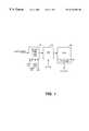
- FIG. 1is a block diagram of one embodiment of the invention.
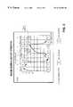
- FIG. 2is a block diagram of the round robin lock logic in one embodiment of the invention.
- FIG. 3shows an exemplary series of loads during an eight cycle period.
- FIG. 4is a timing diagram for a subset of signals in one embodiment of the invention.
- FIG. 1is a block diagram of one embodiment of the invention.
- a content addressable memory array (CAM) 102is used to address into a random access memory unit (RAM) 104 .
- RAMrandom access memory
- the combination of CAM 102 and RAM 104may typically be, for example, a cache and more particularly in one embodiment, a level zero cache, or possibly in an alternate embodiment, a translation lookaside buffer (TLB).
- TLBtranslation lookaside buffer
- the CAM 102contains the addresses corresponding to the corresponding entry, which is a line of code or data in the former case, and a page table entry in the latter.
- the data contained within the CAM entryis referred to as the “tag” entry in either case.
- a control logic unit, such as round robin and lock logic 100is coupled to the CAM 102 .
- the control logic unitcontrols the replacement scheme employed by the CAM addressed cache when data is to be written into the CAM 102 and RAM 104 , e.g., which line is to be replaced on a cache fill operation.
- Both circuits, the CAM 102 and the RAM 104may be written through means well known to those skilled in the art.
- the CAM 102is accessed to determine the matching entry (if there is one) via the content-addressable nature of the CAM 102 . If a match is found, data is read from RAM 104 as output through sense amp 106 , which is coupled thereto, or a write operation to the RAM 104 may be performed through the same circuitry as used to write data into the RAM 104 during the aforementioned fill operation.
- this form of cache circuit architecturehas more favorable low-power characteristics as compared to more typical architectures utilizing RAM cells to store the tag data.
- Round robin and lock logic 100in addition to receiving load requests, receives a number of control signals, including a lock clock, a lock select, a lock clear, and a round robin clear.
- the lock clockwhen asserted indicates that the load request is a lock.
- the loadis a fill.
- lockis a load into a line that is to be locked, so as not to be overwritten by subsequent loads.
- a fillis a load that may be freely overwritten as part of the usual cache replacement scheme.
- Lock clearclears the lock register (discussed further below) to permit the subsequent overwriting of the previous loaded locks.
- Round robin clearresets the round robin register (also discussed further below) to a predetermined value.
- the lock select signalused as the mode select for a set of multiplexers that choose between signals from the round robin registers and the lock registers for word line enablement.
- FIG. 2is a block diagram of the round robin lock logic in one embodiment of the invention.
- the plurality of round robin latches 212 , 214 , 216 , 210are each associated with one line of a cache. In the shown embodiment, it is presumed that there are 32 lines in the array. However, more or fewer lines (and therefore, latches) are within the scope and contemplation of the invention. Accordingly, 32 round robin latches are provided, comprising the round robin register 200 .
- a second plurality of latches, 230 , 232 , 234comprising the lock register 202 , also have one latch associated with each of a plurality of cache lines.
- lock latcheswhich permit the locking of up to 31 of the 32 cache lines. By preventing one or more lines from being locked, the system avoids a deadlock condition in which new data needs to be loaded in the cache, but all lines are locked, preventing such a load.
- the lock latchesare daisy chained together as are the round robin latches. In this manner, the lock register forces an ordered series of locks from top to bottom in the array responsive to the lock clock.
- the round robin register 200cause circular fills beginning with a bottom line in the array followed by the highest unlocked line in the array and proceeding downward to the bottom and then circularly.
- Combinational logic 204ensures that fills do not overwrite locked lines.
- registers 200 and 204are pulsed latches, and in an alternate embodiment, they are master slave flip-flops.
- the pulsed latchesare more area efficient, but tend to be more susceptible to such issues as insufficient hold times over process skews.
- the lock registersinclude the start latch 230 which corresponds to word line 31 of the array in operation has its input coupled to a positive power supply. Thus, when the lock clock is asserted, a high value appears at the output of register 230 , and therefore, correspondingly on the input of register 232 which is daisy chained as shown.
- One issue that arises in an embodiment in using pulsed latches rather than master-slave flipflopsis that sufficient delay must be built into the circuit to avoid both latches 230 and 232 (or more in the chain) from being set when lock clock is asserted.
- lock clockis a short pulse timed to be sufficiently long to allow one latch in the lock register to receive its input value, but sufficiently short to avoid the latch connected to output of the intended target latch from receiving the same data.
- a high valuewill appear at the output of register 232 , as well as 230 .
- the high valuecycles down through the lock register 202 until it reaches lock latch 234 after 31 assertions of the lock clock. At that point, all 31 latches in the lock register 202 will have logical one's stored therein.
- Round robin register 200 latchesare coupled such that after assertion of the round robin reset signal, all latches except latch 210 are cleared.
- Latch 210is the round robin start bit and is set responsive to a round robin clear signal. This signal is also asserted on a full-chip reset to initialize the cache. When latch 210 is set, that necessitates that fills will begin at word line zero.
- the round robin reset signalis asserted responsive to a lock occurring. This ensures that a lock bit cannot be set coincident with the round robin bit which would constitute a logically illegal condition, i.e., that a locked line was selected to be the next target for a line fill. This scheme of setting the bottom, unlockable location for replacement when a lock operation is performed requires a minimum of logic. The implications of this scheme on the cache efficiency is addressed subsequently.
- the next fill lineis identified to be the highest line that is not locked.
- the output of latch 230will be a zero, which will be inverted by inverter 310 causing AND gate 312 to output a “1,” which causes AND gate 314 to also output a “1” to OR gate 316 which will then drive register 212 to output a high value, thereby selecting word line 31 .
- Multiplexers 208employ the lock select signal to determine whether the round robin register or the lock register selects the word lines.
- the word line (WL) selectis chosen to be taken from the output of gate 312 , via the multiplexors 208 and 209 .
- the WL to be asserted, indicating the line to be filled on a lockis based on the coincidence of the previous lock latch being set to logical one and the present one being a logical zero.
- the lock clockis asserted after each lock operation WL assertion.
- the multiplexor 208asserts the WL by passing the logical one contained in the corresponding round robin latch to the WL SELECT node via multiplexor 209 .
- Multiplexor 209selects between the output of multiplexor 208 and a CAM match signal which permits the CAM to assert the WL select during cache read and write operations that utilize the CAM for addressing.
- a decoder outputmay provide the second input to multiplexor 209 .
- start register 210is the only register of the round robin registers with high fanout.
- “high” fanoutis deemed to be more than three inputs to be driven by the output of the device experiencing the fanout.
- Buffer 206is used to buffer up the signal to accommodate the fanout as register 210 must drive an input signal for each of the other round robin registers.
- the other round robin registersdrive inputs only to their nearest neighbors. Consequently, they can be kept very small. This is desirable since there are two latches (in the pulsed-latch embodiment) per line in the cache, a number typically 32 in TLB's, but numbering into the thousands in the case of caches.
- FIG. 3shows an exemplary series of loads during an eight cycle period.
- fill oneis loaded into word line zero, and the fill pointer advances to point to word line 31 .
- fill twois loaded into word line 31 , and the fill pointer is advanced to point to word line 30 .
- fill threeis loaded into word line 30 .
- lock oneis loaded into the lock starting line (word line 31 ), kicking out fill two and the fill pointer is reset to point to word line zero.
- lock twois loaded into the next lock line (word line 30 ), kicking out fill three and again, the fill pointer is reset to point to word line zero.
- fill fouris loaded, kicking out fill one, and the fill pointer is advanced to point to the highest unlocked line, in this case, word line 29 .
- fill fivefills word line 29 .
- lock threekicks out fill five, and the fill pointer is reset to point to word line zero.
- Thisis merely one exemplary fill and lock pattern.
- locks one, two, and threehad been done in the first three cycles with fills one through five done in the next five cycles, no data would have been kicked out of the cache.
- proper software designcan eliminate any potential penalty of restarting the fill portion after each lock. For example, software may lock all code or data which needs to be locked at initialization before filling any cache lines.
- FIG. 4shows a timing diagram of a subset of signals of one embodiment of the invention.
- the pulse clock signal 410is used in the pulse latch embodiment described above.
- the pulseshould be short enough that it will have gone back low before the signal from an adjacent latch can propagate to it neighbor.
- the output of round robin latch ( 212 of FIG. 2)is shown as signal 412 .
- This outputgoes high responsive to the pulse clock 410 .
- the pulse clock 410must be low before the output of OR gate ( 336 of FIG. 1) represented by signal 414 is asserted high based on the application of signal 412 to the OR gate.
- CAMseach with an associated round robin and lock logic unit, are used to form a larger cache having a plurality of banks.
- Each bankimplements the round robin and lock scheme within the bank and independent of all other banks.
Landscapes
- Engineering & Computer Science (AREA)
- Theoretical Computer Science (AREA)
- Physics & Mathematics (AREA)
- General Engineering & Computer Science (AREA)
- General Physics & Mathematics (AREA)
- Memory System Of A Hierarchy Structure (AREA)
- Bus Control (AREA)
- Pharmaceuticals Containing Other Organic And Inorganic Compounds (AREA)
- Accessory Devices And Overall Control Thereof (AREA)
- Materials For Photolithography (AREA)
Abstract
Description
Claims (24)
Priority Applications (9)
| Application Number | Priority Date | Filing Date | Title |
|---|---|---|---|
| US09/476,444US6516384B1 (en) | 1999-12-30 | 1999-12-30 | Method and apparatus to perform a round robin and locking cache replacement scheme |
| KR10-2002-7008325AKR100476446B1 (en) | 1999-12-30 | 2000-11-27 | A method and apparatus to perform a round robin and locking cache replacement scheme |
| CNB008180415ACN1308841C (en) | 1999-12-30 | 2000-11-27 | Method and apparatus for circular and latch cache replacement scheme |
| GB0215661AGB2374178B (en) | 1999-12-30 | 2000-11-27 | A method and apparatus to perform a round robin and locking cache replacement scheme |
| PCT/US2000/042305WO2001050269A2 (en) | 1999-12-30 | 2000-11-27 | A method and apparatus to perform a round robin and locking cache replacement scheme |
| CN200710084018.4ACN101008924B (en) | 1999-12-30 | 2000-11-27 | A method and apparatus to perform a round robin and locking cache replacement scheme |
| JP2001550561AJP2004538536A (en) | 1999-12-30 | 2000-11-27 | Method and apparatus for performing round robin and locking cache replacement |
| AU37936/01AAU3793601A (en) | 1999-12-30 | 2000-11-27 | A method and apparatus to perform a round robin and locking cache replacement scheme |
| TW089128436ATW518464B (en) | 1999-12-30 | 2001-01-09 | A method and apparatus to perform a round robin and locking cache replacement scheme |
Applications Claiming Priority (1)
| Application Number | Priority Date | Filing Date | Title |
|---|---|---|---|
| US09/476,444US6516384B1 (en) | 1999-12-30 | 1999-12-30 | Method and apparatus to perform a round robin and locking cache replacement scheme |
Publications (1)
| Publication Number | Publication Date |
|---|---|
| US6516384B1true US6516384B1 (en) | 2003-02-04 |
Family
ID=23891874
Family Applications (1)
| Application Number | Title | Priority Date | Filing Date |
|---|---|---|---|
| US09/476,444Expired - LifetimeUS6516384B1 (en) | 1999-12-30 | 1999-12-30 | Method and apparatus to perform a round robin and locking cache replacement scheme |
Country Status (8)
| Country | Link |
|---|---|
| US (1) | US6516384B1 (en) |
| JP (1) | JP2004538536A (en) |
| KR (1) | KR100476446B1 (en) |
| CN (2) | CN101008924B (en) |
| AU (1) | AU3793601A (en) |
| GB (1) | GB2374178B (en) |
| TW (1) | TW518464B (en) |
| WO (1) | WO2001050269A2 (en) |
Cited By (10)
| Publication number | Priority date | Publication date | Assignee | Title |
|---|---|---|---|---|
| US20030046627A1 (en)* | 2001-08-22 | 2003-03-06 | Ku Joseph Weiyeh | Digital event sampling circuit and method |
| US6694408B1 (en)* | 2000-05-01 | 2004-02-17 | Javier Villagomez | Scalable replacement method and system in a cache memory |
| US6772199B1 (en)* | 2000-09-14 | 2004-08-03 | International Business Machines Corporation | Method and system for enhanced cache efficiency utilizing selective replacement exemption |
| KR100861691B1 (en) | 2005-12-22 | 2008-10-06 | 인터내셔널 비지네스 머신즈 코포레이션 | Propagating data using mirrored lock caches |
| US20090006784A1 (en)* | 2006-02-28 | 2009-01-01 | Fujitsu Limited | Address exclusive control system and address exclusive control method |
| US20120311276A1 (en)* | 2010-12-14 | 2012-12-06 | Stmicroelectronics S.R.L. | Method for controlling operation of a memory, corresponding system, and computer program product |
| TWI489344B (en)* | 2013-02-25 | 2015-06-21 | Pixart Imaging Inc | Touch control method and touch control apparatus |
| CN105515565A (en)* | 2015-12-14 | 2016-04-20 | 天津光电通信技术有限公司 | Hardware logical resource reuse module and method for realizing reuse |
| US9933947B1 (en)* | 2015-12-30 | 2018-04-03 | EMC IP Holding Company LLC | Maintaining write consistency on distributed multiple page writes |
| US11030104B1 (en)* | 2020-01-21 | 2021-06-08 | International Business Machines Corporation | Picket fence staging in a multi-tier cache |
Families Citing this family (7)
| Publication number | Priority date | Publication date | Assignee | Title |
|---|---|---|---|---|
| CN100424658C (en)* | 2003-11-18 | 2008-10-08 | 松下电器产业株式会社 | Cache memory and its control method |
| US7650466B2 (en)* | 2005-09-21 | 2010-01-19 | Qualcomm Incorporated | Method and apparatus for managing cache partitioning using a dynamic boundary |
| US9448938B2 (en) | 2010-06-09 | 2016-09-20 | Micron Technology, Inc. | Cache coherence protocol for persistent memories |
| US8694737B2 (en) | 2010-06-09 | 2014-04-08 | Micron Technology, Inc. | Persistent memory for processor main memory |
| US8613074B2 (en) | 2010-09-30 | 2013-12-17 | Micron Technology, Inc. | Security protection for memory content of processor main memory |
| FR3086409A1 (en) | 2018-09-26 | 2020-03-27 | Stmicroelectronics (Grenoble 2) Sas | METHOD FOR MANAGING THE PROVISION OF INFORMATION, PARTICULARLY INSTRUCTIONS, TO A MICROPROCESSOR AND CORRESPONDING SYSTEM |
| CN110727463B (en)* | 2019-09-12 | 2021-08-10 | 无锡江南计算技术研究所 | Zero-level instruction circular buffer prefetching method and device based on dynamic credit |
Citations (15)
| Publication number | Priority date | Publication date | Assignee | Title |
|---|---|---|---|---|
| US4783735A (en)* | 1985-12-19 | 1988-11-08 | Honeywell Bull Inc. | Least recently used replacement level generating apparatus |
| US5029072A (en) | 1985-12-23 | 1991-07-02 | Motorola, Inc. | Lock warning mechanism for a cache |
| US5353425A (en)* | 1992-04-29 | 1994-10-04 | Sun Microsystems, Inc. | Methods and apparatus for implementing a pseudo-LRU cache memory replacement scheme with a locking feature |
| US5408629A (en)* | 1992-08-13 | 1995-04-18 | Unisys Corporation | Apparatus and method for controlling exclusive access to portions of addressable memory in a multiprocessor system |
| GB2284911A (en) | 1993-12-16 | 1995-06-21 | Plessey Semiconductors Ltd | Flexible lock-down cache. |
| US5787431A (en)* | 1996-12-16 | 1998-07-28 | Borland International, Inc. | Database development system with methods for java-string reference lookups of column names |
| US5913224A (en)* | 1997-02-26 | 1999-06-15 | Advanced Micro Devices, Inc. | Programmable cache including a non-lockable data way and a lockable data way configured to lock real-time data |
| US5928352A (en) | 1996-09-16 | 1999-07-27 | Intel Corporation | Method and apparatus for implementing a fully-associative translation look-aside buffer having a variable numbers of bits representing a virtual address entry |
| US5928343A (en)* | 1990-04-18 | 1999-07-27 | Rambus Inc. | Memory module having memory devices containing internal device ID registers and method of initializing same |
| US5937429A (en)* | 1997-04-21 | 1999-08-10 | International Business Machines Corporation | Cache memory having a selectable cache-line replacement scheme using cache-line registers in a ring configuration with a token indicator |
| US6044478A (en)* | 1997-05-30 | 2000-03-28 | National Semiconductor Corporation | Cache with finely granular locked-down regions |
| US6073182A (en)* | 1998-04-30 | 2000-06-06 | International Business Machines Corporation | Method of resolving deadlocks between competing requests in a multiprocessor using global hang pulse logic |
| US6098152A (en)* | 1997-10-17 | 2000-08-01 | International Business Machines Corporation | Method and apparatus for miss sequence cache block replacement utilizing a most recently used state |
| US6151655A (en)* | 1998-04-30 | 2000-11-21 | International Business Machines Corporation | Computer system deadlock request resolution using timed pulses |
| US6240489B1 (en)* | 1999-02-24 | 2001-05-29 | International Business Machines Corporation | Method for implementing a pseudo least recent used (LRU) mechanism in a four-way cache memory within a data processing system |
Family Cites Families (2)
| Publication number | Priority date | Publication date | Assignee | Title |
|---|---|---|---|---|
| US5761712A (en)* | 1995-06-07 | 1998-06-02 | Advanced Micro Devices | Data memory unit and method for storing data into a lockable cache in one clock cycle by previewing the tag array |
| JPH11184695A (en)* | 1997-12-19 | 1999-07-09 | Nec Corp | Cache memory and method for access to the same |
- 1999
- 1999-12-30USUS09/476,444patent/US6516384B1/ennot_activeExpired - Lifetime
- 2000
- 2000-11-27GBGB0215661Apatent/GB2374178B/ennot_activeExpired - Lifetime
- 2000-11-27WOPCT/US2000/042305patent/WO2001050269A2/enactiveIP Right Grant
- 2000-11-27KRKR10-2002-7008325Apatent/KR100476446B1/ennot_activeExpired - Lifetime
- 2000-11-27AUAU37936/01Apatent/AU3793601A/ennot_activeAbandoned
- 2000-11-27CNCN200710084018.4Apatent/CN101008924B/ennot_activeExpired - Lifetime
- 2000-11-27JPJP2001550561Apatent/JP2004538536A/enactivePending
- 2000-11-27CNCNB008180415Apatent/CN1308841C/ennot_activeExpired - Lifetime
- 2001
- 2001-01-09TWTW089128436Apatent/TW518464B/ennot_activeIP Right Cessation
Patent Citations (15)
| Publication number | Priority date | Publication date | Assignee | Title |
|---|---|---|---|---|
| US4783735A (en)* | 1985-12-19 | 1988-11-08 | Honeywell Bull Inc. | Least recently used replacement level generating apparatus |
| US5029072A (en) | 1985-12-23 | 1991-07-02 | Motorola, Inc. | Lock warning mechanism for a cache |
| US5928343A (en)* | 1990-04-18 | 1999-07-27 | Rambus Inc. | Memory module having memory devices containing internal device ID registers and method of initializing same |
| US5353425A (en)* | 1992-04-29 | 1994-10-04 | Sun Microsystems, Inc. | Methods and apparatus for implementing a pseudo-LRU cache memory replacement scheme with a locking feature |
| US5408629A (en)* | 1992-08-13 | 1995-04-18 | Unisys Corporation | Apparatus and method for controlling exclusive access to portions of addressable memory in a multiprocessor system |
| GB2284911A (en) | 1993-12-16 | 1995-06-21 | Plessey Semiconductors Ltd | Flexible lock-down cache. |
| US5928352A (en) | 1996-09-16 | 1999-07-27 | Intel Corporation | Method and apparatus for implementing a fully-associative translation look-aside buffer having a variable numbers of bits representing a virtual address entry |
| US5787431A (en)* | 1996-12-16 | 1998-07-28 | Borland International, Inc. | Database development system with methods for java-string reference lookups of column names |
| US5913224A (en)* | 1997-02-26 | 1999-06-15 | Advanced Micro Devices, Inc. | Programmable cache including a non-lockable data way and a lockable data way configured to lock real-time data |
| US5937429A (en)* | 1997-04-21 | 1999-08-10 | International Business Machines Corporation | Cache memory having a selectable cache-line replacement scheme using cache-line registers in a ring configuration with a token indicator |
| US6044478A (en)* | 1997-05-30 | 2000-03-28 | National Semiconductor Corporation | Cache with finely granular locked-down regions |
| US6098152A (en)* | 1997-10-17 | 2000-08-01 | International Business Machines Corporation | Method and apparatus for miss sequence cache block replacement utilizing a most recently used state |
| US6073182A (en)* | 1998-04-30 | 2000-06-06 | International Business Machines Corporation | Method of resolving deadlocks between competing requests in a multiprocessor using global hang pulse logic |
| US6151655A (en)* | 1998-04-30 | 2000-11-21 | International Business Machines Corporation | Computer system deadlock request resolution using timed pulses |
| US6240489B1 (en)* | 1999-02-24 | 2001-05-29 | International Business Machines Corporation | Method for implementing a pseudo least recent used (LRU) mechanism in a four-way cache memory within a data processing system |
Cited By (15)
| Publication number | Priority date | Publication date | Assignee | Title |
|---|---|---|---|---|
| US6694408B1 (en)* | 2000-05-01 | 2004-02-17 | Javier Villagomez | Scalable replacement method and system in a cache memory |
| US6772199B1 (en)* | 2000-09-14 | 2004-08-03 | International Business Machines Corporation | Method and system for enhanced cache efficiency utilizing selective replacement exemption |
| US20030046627A1 (en)* | 2001-08-22 | 2003-03-06 | Ku Joseph Weiyeh | Digital event sampling circuit and method |
| US6889349B2 (en)* | 2001-08-22 | 2005-05-03 | Hewlett-Packard Development Company, L.P. | Digital event sampling circuit and method |
| KR100861691B1 (en) | 2005-12-22 | 2008-10-06 | 인터내셔널 비지네스 머신즈 코포레이션 | Propagating data using mirrored lock caches |
| US8082410B2 (en)* | 2006-02-28 | 2011-12-20 | Fujitsu Limited | Address exclusive control system and address exclusive control method |
| US20090006784A1 (en)* | 2006-02-28 | 2009-01-01 | Fujitsu Limited | Address exclusive control system and address exclusive control method |
| US20120311276A1 (en)* | 2010-12-14 | 2012-12-06 | Stmicroelectronics S.R.L. | Method for controlling operation of a memory, corresponding system, and computer program product |
| US9081514B2 (en)* | 2010-12-14 | 2015-07-14 | Stmicroelectronics S.R.L. | Method for controlling operation of a memory using a single write location and an associated memory |
| TWI489344B (en)* | 2013-02-25 | 2015-06-21 | Pixart Imaging Inc | Touch control method and touch control apparatus |
| CN105515565A (en)* | 2015-12-14 | 2016-04-20 | 天津光电通信技术有限公司 | Hardware logical resource reuse module and method for realizing reuse |
| CN105515565B (en)* | 2015-12-14 | 2018-07-13 | 天津光电通信技术有限公司 | A kind of method that hardware logic resource multiplex module and multiplexing are realized |
| US9933947B1 (en)* | 2015-12-30 | 2018-04-03 | EMC IP Holding Company LLC | Maintaining write consistency on distributed multiple page writes |
| US10620842B1 (en)* | 2015-12-30 | 2020-04-14 | EMC IP Holding Company LLC | Maintaining write consistency on distributed multiple page writes |
| US11030104B1 (en)* | 2020-01-21 | 2021-06-08 | International Business Machines Corporation | Picket fence staging in a multi-tier cache |
Also Published As
| Publication number | Publication date |
|---|---|
| CN101008924A (en) | 2007-08-01 |
| TW518464B (en) | 2003-01-21 |
| KR100476446B1 (en) | 2005-03-16 |
| JP2004538536A (en) | 2004-12-24 |
| CN101008924B (en) | 2015-05-13 |
| KR20020097145A (en) | 2002-12-31 |
| CN1415093A (en) | 2003-04-30 |
| GB2374178B (en) | 2004-08-25 |
| GB2374178A (en) | 2002-10-09 |
| WO2001050269A2 (en) | 2001-07-12 |
| GB0215661D0 (en) | 2002-08-14 |
| CN1308841C (en) | 2007-04-04 |
| AU3793601A (en) | 2001-07-16 |
| WO2001050269A3 (en) | 2001-12-13 |
Similar Documents
| Publication | Publication Date | Title |
|---|---|---|
| US6516384B1 (en) | Method and apparatus to perform a round robin and locking cache replacement scheme | |
| US5510934A (en) | Memory system including local and global caches for storing floating point and integer data | |
| US6223228B1 (en) | Apparatus for synchronizing multiple processors in a data processing system | |
| JP3504282B2 (en) | Integrated circuit chip providing real-time cache function | |
| EP1278125A2 (en) | Indexing and multiplexing of interleaved cache memory arrays | |
| US7073026B2 (en) | Microprocessor including cache memory supporting multiple accesses per cycle | |
| JP4298800B2 (en) | Prefetch management in cache memory | |
| JPH04230551A (en) | Cache memory of hierarchical integrated circuit | |
| JP4445081B2 (en) | Cache memory | |
| US9558121B2 (en) | Two-level cache locking mechanism | |
| JPH0362144A (en) | Method for speeding up memory access in an information processing system and system for implementing this method | |
| EP3583486B1 (en) | Super-thread processor | |
| Garside et al. | The AMULET2e cache system | |
| US5550995A (en) | Memory cache with automatic alliased entry invalidation and method of operation | |
| US6823430B2 (en) | Directoryless L0 cache for stall reduction | |
| US6249880B1 (en) | Method and apparatus for exhaustively testing interactions among multiple processors | |
| US6230263B1 (en) | Data processing system processor delay instruction | |
| US7500066B2 (en) | Method and apparatus for sharing instruction memory among a plurality of processors | |
| WO2000016183A1 (en) | Calendar clock caching in a multiprocessor system | |
| JP2001256109A (en) | Method and device for controlling integrated cache port | |
| US7234027B2 (en) | Instructions for test & set with selectively enabled cache invalidate | |
| US6694408B1 (en) | Scalable replacement method and system in a cache memory | |
| US5388226A (en) | Method and apparatus for accessing a register in a data processing system | |
| US7124236B1 (en) | Microprocessor including bank-pipelined cache with asynchronous data blocks | |
| HK1110404A (en) | A method and apparatus to perform a round robin and locking cache replacement scheme |
Legal Events
| Date | Code | Title | Description |
|---|---|---|---|
| AS | Assignment | Owner name:INTEL CORPORATION, CALIFORNIA Free format text:ASSIGNMENT OF ASSIGNORS INTEREST;ASSIGNORS:CLARK, LAWRENCE T.;CLARK, MATTHEW M.;REEL/FRAME:010603/0899 Effective date:20000223 | |
| STCF | Information on status: patent grant | Free format text:PATENTED CASE | |
| FEPP | Fee payment procedure | Free format text:PAYOR NUMBER ASSIGNED (ORIGINAL EVENT CODE: ASPN); ENTITY STATUS OF PATENT OWNER: LARGE ENTITY | |
| FPAY | Fee payment | Year of fee payment:4 | |
| AS | Assignment | Owner name:MARVELL INTERNATIONAL LTD.,BERMUDA Free format text:ASSIGNMENT OF ASSIGNORS INTEREST;ASSIGNOR:INTEL CORPORATION;REEL/FRAME:018515/0817 Effective date:20061108 Owner name:MARVELL INTERNATIONAL LTD., BERMUDA Free format text:ASSIGNMENT OF ASSIGNORS INTEREST;ASSIGNOR:INTEL CORPORATION;REEL/FRAME:018515/0817 Effective date:20061108 | |
| AS | Assignment | Owner name:MARVELL WORLD TRADE LTD.,BARBADOS Free format text:ASSIGNMENT OF ASSIGNORS INTEREST;ASSIGNOR:MARVELL INTERNATIONAL LTD.;REEL/FRAME:018635/0333 Effective date:20061212 Owner name:MARVELL INTERNATIONAL LTD.,BERMUDA Free format text:LICENSE;ASSIGNOR:MARVELL WORLD TRADE LTD.;REEL/FRAME:018635/0621 Effective date:20061212 Owner name:MARVELL INTERNATIONAL LTD., BERMUDA Free format text:LICENSE;ASSIGNOR:MARVELL WORLD TRADE LTD.;REEL/FRAME:018635/0621 Effective date:20061212 Owner name:MARVELL WORLD TRADE LTD., BARBADOS Free format text:ASSIGNMENT OF ASSIGNORS INTEREST;ASSIGNOR:MARVELL INTERNATIONAL LTD.;REEL/FRAME:018635/0333 Effective date:20061212 | |
| FPAY | Fee payment | Year of fee payment:8 | |
| FPAY | Fee payment | Year of fee payment:12 | |
| AS | Assignment | Owner name:MARVELL INTERNATIONAL LTD., BERMUDA Free format text:ASSIGNMENT OF ASSIGNORS INTEREST;ASSIGNOR:MARVELL WORLD TRADE LTD.;REEL/FRAME:051778/0537 Effective date:20191231 | |
| AS | Assignment | Owner name:CAVIUM INTERNATIONAL, CAYMAN ISLANDS Free format text:ASSIGNMENT OF ASSIGNORS INTEREST;ASSIGNOR:MARVELL INTERNATIONAL LTD.;REEL/FRAME:052918/0001 Effective date:20191231 | |
| AS | Assignment | Owner name:MARVELL ASIA PTE, LTD., SINGAPORE Free format text:ASSIGNMENT OF ASSIGNORS INTEREST;ASSIGNOR:CAVIUM INTERNATIONAL;REEL/FRAME:053475/0001 Effective date:20191231 |