US6515909B1 - Flash memory device with a variable erase pulse - Google Patents
Flash memory device with a variable erase pulseDownload PDFInfo
- Publication number
- US6515909B1 US6515909B1US09/972,426US97242601AUS6515909B1US 6515909 B1US6515909 B1US 6515909B1US 97242601 AUS97242601 AUS 97242601AUS 6515909 B1US6515909 B1US 6515909B1
- Authority
- US
- United States
- Prior art keywords
- flash cell
- erase
- flash
- length
- short
- Prior art date
- Legal status (The legal status is an assumption and is not a legal conclusion. Google has not performed a legal analysis and makes no representation as to the accuracy of the status listed.)
- Expired - Lifetime
Links
- 238000000034methodMethods0.000claimsabstractdescription104
- 230000003247decreasing effectEffects0.000claimsabstractdescription23
- 238000006243chemical reactionMethods0.000claimsdescription23
- 230000007423decreaseEffects0.000claimsdescription7
- 230000004044responseEffects0.000claimsdescription7
- 238000007667floatingMethods0.000description29
- 239000000758substrateSubstances0.000description25
- 239000004065semiconductorSubstances0.000description17
- 239000000463materialSubstances0.000description10
- 238000004364calculation methodMethods0.000description9
- 238000010586diagramMethods0.000description9
- 239000010410layerSubstances0.000description7
- 238000009792diffusion processMethods0.000description6
- 235000012431wafersNutrition0.000description6
- XUIMIQQOPSSXEZ-UHFFFAOYSA-NSiliconChemical compound[Si]XUIMIQQOPSSXEZ-UHFFFAOYSA-N0.000description4
- 230000032683agingEffects0.000description4
- 230000008901benefitEffects0.000description4
- 230000008859changeEffects0.000description4
- 239000012212insulatorSubstances0.000description4
- 229910052710siliconInorganic materials0.000description4
- 239000010703siliconSubstances0.000description4
- 230000005669field effectEffects0.000description3
- 229910021420polycrystalline siliconInorganic materials0.000description3
- 238000009825accumulationMethods0.000description2
- 238000004891communicationMethods0.000description2
- 230000008878couplingEffects0.000description2
- 238000010168coupling processMethods0.000description2
- 238000005859coupling reactionMethods0.000description2
- 229920005591polysiliconPolymers0.000description2
- 230000005689Fowler Nordheim tunnelingEffects0.000description1
- 238000003491arrayMethods0.000description1
- 230000001413cellular effectEffects0.000description1
- 230000000295complement effectEffects0.000description1
- 239000004020conductorSubstances0.000description1
- 230000007812deficiencyEffects0.000description1
- 230000002950deficientEffects0.000description1
- 238000005516engineering processMethods0.000description1
- 239000002784hot electronSubstances0.000description1
- 238000002347injectionMethods0.000description1
- 239000007924injectionSubstances0.000description1
- 238000004519manufacturing processMethods0.000description1
- 229910021421monocrystalline siliconInorganic materials0.000description1
- 239000002344surface layerSubstances0.000description1
- 239000010409thin filmSubstances0.000description1
- 238000005406washingMethods0.000description1
Images


Classifications
- G—PHYSICS
- G11—INFORMATION STORAGE
- G11C—STATIC STORES
- G11C16/00—Erasable programmable read-only memories
- G11C16/02—Erasable programmable read-only memories electrically programmable
- G11C16/06—Auxiliary circuits, e.g. for writing into memory
- G11C16/34—Determination of programming status, e.g. threshold voltage, overprogramming or underprogramming, retention
- G11C16/3436—Arrangements for verifying correct programming or erasure
- G11C16/344—Arrangements for verifying correct erasure or for detecting overerased cells
- G11C16/3445—Circuits or methods to verify correct erasure of nonvolatile memory cells
- G—PHYSICS
- G11—INFORMATION STORAGE
- G11C—STATIC STORES
- G11C16/00—Erasable programmable read-only memories
- G11C16/02—Erasable programmable read-only memories electrically programmable
- G11C16/06—Auxiliary circuits, e.g. for writing into memory
- G11C16/10—Programming or data input circuits
- G11C16/14—Circuits for erasing electrically, e.g. erase voltage switching circuits
- G11C16/16—Circuits for erasing electrically, e.g. erase voltage switching circuits for erasing blocks, e.g. arrays, words, groups
- G—PHYSICS
- G11—INFORMATION STORAGE
- G11C—STATIC STORES
- G11C16/00—Erasable programmable read-only memories
- G11C16/02—Erasable programmable read-only memories electrically programmable
- G11C16/06—Auxiliary circuits, e.g. for writing into memory
- G11C16/34—Determination of programming status, e.g. threshold voltage, overprogramming or underprogramming, retention
- G11C16/3436—Arrangements for verifying correct programming or erasure
- G11C16/344—Arrangements for verifying correct erasure or for detecting overerased cells
Definitions
- the present inventionrelates generally to memory devices, and more particularly, to a flash memory device with a variable erase pulse.
- a flash memory deviceis typically formed in an integrated circuit.
- a conventional flash cellalso called a floating gate transistor memory cell, is similar to a field effect transistor, having a channel region between a source and a drain in a substrate and a control gate over the channel region.
- the flash cellhas a floating gate between the control gate and the channel region. The floating gate is separated from the channel region by a layer of gate oxide, and an inter-poly dielectric layer separates the control gate from the floating gate. Both the control gate and the floating gate are formed of doped polysilicon.
- the floating gateis floating or electrically isolated.
- the flash memory devicehas a large number of flash cells in an array where the control gate of each flash cell is connected to a word line and the drain is connected to a bit line, the flash cells being arranged in a grid of word lines and bit lines.
- a flash cellis programmed by applying approximately 10 volts to the control gate, between 5 and 7 volts to the drain, and grounding the source and the substrate to induce hot electron injection from the channel region to the floating gate through the gate oxide.
- the voltage at the control gatedetermines the amount of charge residing on the floating gate after programming.
- the chargeaffects current in the channel region by determining the voltage that must be applied to the control gate in order to allow the flash cell to conduct current between the source and the drain. This voltage is termed the threshold voltage of the flash cell, and is the physical form of the data stored in the flash cell. As the charge on the floating gate increases the threshold voltage increases.
- One type of flash memory deviceincludes an array of multi-bit or multi-state flash cells.
- Multi-state flash cellshave the same structure as ordinary flash cells and are capable of storing multiple bits of data in a single cell.
- a multi-bit or multi-state flash cellhas multiple distinct threshold voltage levels over a voltage range. Each distinct threshold voltage level corresponds to a set of data bits, with the number of bits representing the amount of data which can be stored in the multi-state flash cell.
- Datais stored in conventional flash memory devices by programming flash cells that have been previously erased.
- a flash cellis erased by applying an erase pulse of approximately ⁇ 10 volts to the control gate, applying approximately 5 volts to the source, grounding the substrate and allowing the drain to float.
- the control gateis grounded and an erase pulse of approximately 12 volts is applied to the source.
- the electrons in the floating gateare induced to pass through the gate oxide to the source by Fowler-Nordheim tunneling such that the charge in the floating gate is reduced and the threshold voltage of the flash cell is reduced.
- the flash cellis then read in a manner described below to determine if it is erased. If the flash cell is not erased, another erase pulse is applied to the flash cell.
- a flash cellis read by applying approximately 5 volts to the control gate, approximately 1 volt to the drain, and grounding the source and the substrate.
- the flash cellis rendered conductive and current between the source and the drain is sensed to determine data stored in the flash cell.
- the currentis converted to a voltage that is compared with one or more reference voltages in a sense amplifier to determine the state of the flash cell.
- the current drawn by a flash cell being readdepends on the amount of charge stored in the floating gate.
- flash memory devicesAs flash memory devices age with use they tend to wear, or change physically, and their operational characteristics change. The operational efficiency of a flash memory device can decline over time due to these changes in its physical and operational characteristics. There remains a need for a flash memory device that may be operated efficiently over its entire operating life.
- a method of operating a flash memory deviceincludes selecting a flash cell in a flash memory device to undergo an erase, applying a long erase pulse to the flash cell, and reading the flash cell. For each time the flash cell is read and is not in an erased state, the method includes applying a short erase pulse to the flash cell, counting the short erase pulse, and reading the flash cell. Finally, a length of the long erase pulse is adjusted based on the counted number of short erase pulses that were applied to the flash cell.
- the length of the long erase pulsemay be increased if the counted number of short erase pulses is more than a high number of pulses, or it may be decreased if the counted number of short erase pulses is less than a low number of pulses.
- the length of the long erase pulsemay be adjusted based on a past average of short erase pulses applied to the flash cell, or a quantity representing short erase pulses applied to the flash cell over a selected number of prior erases of the flash cell.
- the flash memory devicemay have a control circuit with elements to implement the method.
- FIG. 1is a block diagram of a flash memory system according to an embodiment of the present invention.
- FIG. 2is a cross-sectional view of a flash cell according to an embodiment of the present invention.
- FIG. 3is an electrical schematic diagram of a block of flash cells in the memory system of FIG. 1 according to an embodiment of the present invention.
- FIG. 4is a plot of erase pulses to be applied to a flash cell to erase the flash cell according to an embodiment of the present invention.
- FIG. 5is a flowchart of a method of erasing a flash cell according to an embodiment of the present invention.
- FIG. 6is an electrical schematic diagram of a read circuit for reading flash cells according to an embodiment of the present invention.
- FIG. 7is a flowchart of a method of adjusting a long erase pulse according to an embodiment of the present invention.
- FIG. 8is a flowchart of a method of adjusting a long erase pulse according to an embodiment of the present invention.
- FIG. 9is a flowchart of a method of calculating a quantity to adjust a long erase pulse according to an embodiment of the present invention.
- FIG. 10is a flowchart of a method of calculating a quantity to adjust a long erase pulse according to an embodiment of the present invention.
- FIG. 11is a flowchart of a method of calculating a quantity to adjust a long erase pulse according to an embodiment of the present invention.
- FIG. 12is a block diagram of an integrated circuit chip according to an embodiment of the present invention.
- FIG. 13is block diagram of a flash memory card according to an embodiment of the present invention.
- FIG. 14is a block diagram of an information-handling system according to an embodiment of the present invention.
- a threshold voltage of a transistoris the voltage that must be applied to a control gate of the transistor in order to allow the transistor to conduct current between a source and a drain.
- a transistor or a flash cellis described as being in an active state or activated or switched on when it is rendered conductive by a control gate voltage that exceeds its threshold voltage, and the transistor or flash cell is described as being in an inactive state or switched off when the control gate voltage is below the threshold voltage and the transistor or flash cell is non-conductive.
- a digital signal of 1may also be called a high signal and a digital signal of 0 may also be called a low signal.
- wafer and substratemay be used in the following description and include any structure having an exposed surface with which to form an integrated circuit (IC) according to embodiments of the present invention.
- substrateis understood to include semiconductor wafers.
- substrateis also used to refer to semiconductor structures during fabrication, and may include other layers that have been fabricated thereupon.
- substrateincludes doped and undoped semiconductors, epitaxial semiconductor layers supported by a base semiconductor, or semiconductor layers supported by an insulator, as well as other semiconductor structures well known to one skilled in the art.
- insulatoris defined to include any material that is less electrically conductive than materials generally referred to as conductors by those skilled in the art.
- horizontalas used in this application is defined as a plane substantially parallel to the conventional plane or surface of a wafer or substrate, regardless of the orientation of the wafer or substrate.
- verticalrefers to a direction substantially perpendicular to the horizonal as defined above. Prepositions, such as “on,” “upper,” “side” (as in “sidewall”), “higher,” “lower,” “over” and “under” are defined with respect to the conventional plane or surface being on the top surface of the wafer or substrate, regardless of the orientation of the wafer or substrate.
- source/drainrefers generally to the terminals or diffusion regions of a field effect transistor.
- a terminal or a diffusion regionmay be more specifically described as a “source” or a “drain” on the basis of a voltage applied to it when the field effect transistor is in operation.
- n-type conductivityis conductivity associated with holes in a semiconductor material
- n-type conductivityis conductivity associated with electrons in a semiconductor material.
- n+refers to semiconductor material that is heavily doped n-type semiconductor material, e.g., monocrystalline silicon or polycrystalline silicon.
- p+refers to semiconductor material that is heavily doped p-type semiconductor material.
- n ⁇ and p ⁇refer to lightly doped n and p-type semiconductor materials, respectively.
- a diffusion region in a substrate described herein according to embodiments of the present inventionmay also be called a moat or a well or a tank.
- the diffusion regionmay be an n-type diffusion region or a p-type diffusion region, and the substrate may be a silicon substrate.
- Transistors and other devices described herein according to embodiments of the present inventionmay have moats or wells that may be formed in other moats or wells or tanks rather than substrates. Such moats or wells or tanks may be situated with other moats or wells or tanks, or within other moats or wells or tanks, in a larger substrate.
- the moats or wells or tanksmay also be situated in a silicon-on-insulator (SOI) device.
- SOIsilicon-on-insulator
- FIG. 1is a block diagram of a flash memory system 100 according to an embodiment of the present invention.
- the memory system 100includes a memory controller 105 and a flash memory integrated circuit (IC) 110 .
- the controller 105includes a control device such as a microprocessor to provide interface signals to the IC 110 .
- the interface signalsinclude address signals provided over multiple address lines A 0 -A 20 to an address buffer and latch 116 , and data signals communicated over multiple data lines DATA ⁇ 7:0>.
- the IC 110has more than 21 address lines, and more than 8 data lines in alternate embodiments of the present invention.
- the data lines DATA ⁇ 7:0>are coupled to an input buffer 118 which stores the data signals for transfer to an input data latch 119 over multiple internal data lines 120 .
- Other interface signals provided by the controller 105include a write enable signal WE* at node 121 , a chip enable signal CE* at node 122 , a reset/power-down signal RP* at node 123 , an output enable signal OE* at node 124 , and a write protect signal WP* at node 125 , all of which are active low signals.
- the IC 110provides a status signal RY/BY* to the controller 105 at node 128 to indicate the status of an internal state machine 130 .
- the IC 110also receives a positive power supply voltage V cc at node 132 , a write/erase supply or programming voltage V pp at node 134 , and a reference voltage such as a substrate ground voltage V ss at node 136 which is approximately 0 Volts.
- V ccpositive power supply voltage
- V ppwrite/erase supply or programming voltage
- V ppwrite/erase supply or programming voltage
- V ppwrite/erase supply or programming voltage
- V ppwrite/erase supply or programming voltage
- the IC 110includes an array 138 of floating gate transistor memory cells or flash cells arranged in 32 flash cell blocks. Each block in the array 138 contains 64 kilobytes of flash cells.
- a command execution logic module 140receives the above-described interface signals from the controller 105 .
- the module 140controls the state machine 130 which controls individual acts necessary for programming, reading, and erasing the flash cells in the array 138 . More specifically, the state machine 130 controls detailed operations of the IC 110 such as providing write and block erase timing sequences to the array 138 through an X-interface circuit 145 and a Y-interface circuit 150 .
- the Y-interface circuit 150provides access to individual flash cells through bit lines in the array 138 . Bit lines in the Y-interface circuit 150 are connected to a bit line driver circuit (not shown).
- the Y-interface circuit 150includes a Y-decoder circuit 152 , Y-select gates 154 , and sense amplifiers and write/erase bit compare and verify circuits 156 .
- the X-interface circuit 145provides access to rows of flash cells through word lines in the array 138 , which are electrically coupled to the control gates of the flash cells in the array 138 .
- the X-interface circuit 145includes decoding and control circuits for erasing the flash cells in the array 138 .
- the write/erase bit compare and verify circuits 156are coupled to exchange data with the input data latch 119 over a set of internal data lines 158 .
- the IC 110includes a charge pump circuit 160 to generate an elevated voltage Vpump for programming, erasing, or reading the flash cells in the array 138 .
- the pump circuit 160is coupled to receive the positive power supply voltage V cc from the node 132 and provides the voltage Vpump to the X-interface circuit 145 , the Y-decoder circuit 152 , and the state machine 130 over a plurality of lines.
- the pump circuit 160may provide a different elevated voltage over each of the lines shown in FIG. 1 .
- the state machine 130controls an address counter 162 which is capable of providing a sequence of addresses on an internal set of address lines 164 coupled between the address buffer and latch 116 , the X-interface circuit 145 , and the Y-decoder circuit 152 .
- the IC 110also includes a status register 170 coupled to receive signals from the state machine 130 , the module 140 , and the pump circuit 160 . Bits in the status register 170 indicate the status of the IC 110 , and the status register 170 is read by the controller 105 .
- the IC 110also includes an identification register 172 coupled to receive signals from the module 140 .
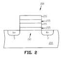
- FIG. 2A cross-sectional view of a flash cell 200 is shown in FIG. 2 according to an embodiment of the present invention.
- the flash cell 200includes an n+-type source S and an n+-type drain D formed in a p-type silicon substrate 210 .
- the source S and the drain Dare separated by a channel region 212 in the substrate 210 .
- the flash cell 200includes a floating gate 215 and a control gate 220 , both formed of doped polysilicon.
- the floating gate 215is floating or electrically isolated.
- a layer of gate oxide 225separates the floating gate 215 from the channel region 212 in the substrate 210 .
- An inter-poly dielectric layer 235separates the floating gate 215 from the control gate 220 .
- the substrate 210may be silicon or another semiconductor material, or it may be a thin semiconductor surface layer formed on an underlying insulating portion, such as a semiconductor-on-insulator (SOI) structure or other thin film transistor technology.
- SOIsemiconductor-on-insulator
- the source S and the drain Dare formed by conventional complementary metal-oxide-semiconductor (CMOS) processing techniques.
- CMOScomplementary metal-oxide-semiconductor
- the flash cell 200 shown in FIG. 2is an n-channel floating gate transistor memory cell.
- the flash cell 200may be a p-channel floating gate transistor memory cell with a p+-type source S and a p+-type drain D formed in an n-type silicon substrate 210 .
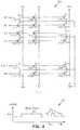
- FIG. 3is an electrical schematic diagram of a block 300 of flash cells 310 A- 310 S in the array 138 according to an embodiment of the present invention. Some flash cells in the block 300 are omitted from FIG. 3 for purposes of clarity.
- the flash cells 310are arranged in rows and columns. All of the flash cells 310 in a particular column have drains D connected to a common bit line BL and all of the flash cells 310 in a particular row have control gates connected to a common word line WL.
- the bit lines BLare identified as BL 0 -BLM and the word lines WL are identified as WL 0 -WLN. All of the flash cells 310 in the block 300 have sources S connected to a common source line SL.
- the remaining flash cells in the array 138are arranged into separate blocks having separate source lines. There may be more or less flash cells 310 in the block 300 , and in the array 138 , according to alternate embodiments of the present invention.
- the flash cells 310are arranged in column pairs, with each flash cell 310 of the pair sharing a common source S.
- a flash cell pair 310 J and 310 Khave a common source S connected to the source line SL.
- the drains D of the flash cells 310are connected to the bit line BL associated with the column in which the flash cells 310 are located.
- the flash cell pair 310 J and 310 Khave their drains D connected to a common bit line BL 1 .
- One of the flash cells 310 A- 310 S in the block 300is selected according to address signals on the address lines A 0 -A 20 that identify the flash cell.
- the flash cellis selected by the X-interface circuit 145 that selects a word line and by the Y-interface circuit 150 that selects a bit line in response to the address signals.
- the word line and the bit lineare coupled to the flash cell.
- a selected one of the flash cells 310 A- 310 S in the block 300is programmed by holding the source line SL to the ground voltage V ss or zero volts, coupling approximately 5-7 volts to the bit line BL connected to the flash cell, and applying a high positive voltage programming pulse of approximately 10 volts to the word line WL of the flash cell.
- a selected one of the flash cells 310 A- 310 S in the block 300is read by holding the source line SL to the ground voltage V ss , coupling approximately 1 volt to the bit line BL connected to the flash cell, applying approximately 5.4 volts to the word line WL of the flash cell, and sensing current in the flash cell through the bit line BL.
- the currentis sensed by one of the sense amplifiers 156 that is coupled to the bit line BL.
- the sensed currentis inversely related to the threshold voltage of the flash cell. The higher the threshold voltage, the less current is sensed in the flash cell, and visa versa.
- a selected one of the flash cells 310 A- 310 S in the block 300may be erased by holding the source line SL to approximately 5 volts, allowing the bit line BL connected to the flash cell to float, and applying an erase pulse of approximately ⁇ 10 volts to the word line WL of the flash cell.
- the flash cells 310 A- 310 S in the block 300may also be erased by holding the word lines WL 0 -WLN to the ground voltage V ss , allowing the bit lines BL 0 -BLM to float, and applying a high positive voltage erase pulse of approximately 12 volts to the sources S through the source line SL. Charge is removed from the floating gate of the flash cell when it is erased.
- Flash memory devicesage over time and wear with use such that their structure and operational characteristics slowly change.
- the structure of a flash cellis changed each time it is programmed or erased, and the accumulation of cycles of programs and erasures is a significant cause of aging. Changes in the flash memory device also result from fluctuations in temperature or operating voltages. Operational parameters that are efficient in the early operating life of a flash memory device may result in less efficient operation as the flash memory device changes with age. For example, a flash cell will slow down and need longer and longer erase times as it ages. Aging of the flash cell is accelerated if it is under-erased periodically. An under-erased flash cell has too much charge on its floating gate and must be erased again.
- the repeated erasing of the flash cellcontributes to its wear. Aging of the flash cell is also accelerated if it is over-erased one or more times during its operating life.
- a flash cellcan be over-erased by a series of erase pulses that remove too much charge from the floating gate.
- An over-erased flash cellhas insufficient negative charge in the floating gate, and in some cases may have a net positive charge in the floating gate, and therefore has a threshold voltage that is too low.
- the over-erased flash cellwill be activated with a very low positive voltage applied to the control gate, even as low as a ground voltage, and may leak current even though it is not being read or verified. Leaking current is current that is allowed to pass through the flash cell when the flash cell is not intended to be active.
- the current from leaking flash cellsmakes it impossible to read other flash cells accurately if they share a bit line, the line connecting the drains of adjacent flash cells to a sense amplifier.
- the over-erased flash cellis corrected with a heal operation or by soft programming, and both operations take a substantial amount of time. Furthermore, each time a flash cell is over-erased the heal operation or soft programming causes additional wear on the flash cell, further altering its operating condition and making it more susceptible to being over-erased.
- the operating life of a flash memory deviceis limited by the physical changes it undergoes as it ages, and ends when the flash memory device is no longer operable due to the accumulation of such changes.
- an erase pulseis a voltage applied to a control gate or a source of a flash cell to erase the flash cell.
- a length of the erase pulseis the period of time during which it is applied. The voltage of the erase pulse remains approximately constant for the length of the erase pulse.
- An erase pulse of approximately ⁇ 10 voltsmay be applied to the control gate of the flash cell to erase the flash cell.
- approximately 5 voltsis applied concurrently to the source, the substrate is coupled to a ground voltage reference, and the drain floats, or is electrically isolated when the erase pulse is applied to the control gate.
- An erase pulse of approximately 12 voltsmay instead be applied to the source of the flash cell to erase the flash cell.
- the substrate and the control gateare coupled to a ground voltage reference and the drain floats.
- FIG. 4is a plot 400 of erase pulses to be applied to a flash cell to erase the flash cell.
- the flash cell discussed hereinis similar to the flash cell 200 described above and shown in FIG. 2 .
- Timeis shown with reference to a horizontal axis 402
- voltageis shown with reference to a vertical axis 404 .
- the erase pulsesinclude a long erase pulse 410 followed by several short erase pulses 412 .
- the long erase pulse 410removes a substantial portion of charge from the floating gate and leaves it almost or nearly erased.
- the long erase pulse 410brings the floating gate to the brink of being erased.
- the short erase pulses 412are then applied to finally erase the flash cell according to a method shown in FIG. 5 .
- the long erase pulse 410may be 10 microseconds long, and each short erase pulse may be between 0.5 microseconds and 2.0 microseconds according to an embodiment of the present invention.
- the short erase pulsesmay all be the same length, or may vary in length according to alternate embodiments of the present invention.
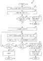
- FIG. 5A flowchart of a method 500 of erasing a flash cell is shown in FIG. 5 according to an embodiment of the present invention.
- the method 500starts in 502 and a long erase pulse is applied to the flash cell in 504 .
- the flash cellis read in 506 and the method 500 determines in 508 if the flash cell is erased based on the read in 506 . If the flash cell is erased, the method 500 determines whether the flash cell is over-erased in 510 before ending in 512 . If it is determined in 508 that the flash cell is not erased, a counter is initialized in 520 and a short erase pulse is applied to the flash cell in 522 .
- the flash cellis read and the counter is incremented in 524 .
- the method 500determines in 526 if the flash cell is erased based on the read in 524 . If the flash cell is not erased, the method 500 determines in 528 whether the counter has exceeded a limit, and if so, an error is indicated in 530 indicating that the flash cell is defective, and the method ends in 532 . If the counter has not exceeded the limit in 528 , the method 500 returns to 522 to apply another short erase pulse to the flash cell. The method 500 repeats the loop of 522 - 528 and returns to 522 to apply short erase pulses to the flash cell until the flash cell is shown to be erased by the read in 524 , or the counter exceeds the limit in 528 .
- the methodstores the value of the counter in a memory such as a register and adjusts the long erase pulse in 540 based on the counter, or more specifically the value of the counter indicating how many short erase pulses have been applied to the flash cell.
- the method 500determines whether the flash cell is over-erased in 542 before ending in 544 .
- the flash cellis read in 506 and 524 with a read circuit 600 shown in FIG. 6 according to an embodiment of the present invention.
- the read circuit 600is located in the IC 110 , and may be in the sense amplifiers 156 shown in FIG. 1 .
- the flash cellis selected according to address signals on the address lines A 0 -A 20 , and is read by applying approximately 5.4 volts to its control gate and sensing a current I in the flash cell.
- the current I from the flash cellis received on a line 610 and is converted to a voltage signal, also called a read signal, by a first current to voltage conversion circuit 612 .
- the first current to voltage conversion circuit 612generates a low read signal if the current I is high, and a high read signal if the current I is low.
- the read signalis coupled to an inverting input of a sense amplifier 614 .
- the sense amplifier 614is a comparator in this embodiment of the present invention.
- a reference current I Ris generated in a current source 620 to be approximately equal to current in the flash cell if it had a threshold voltage of 4.0 volts. In one embodiment of the present invention, I R is 30 microamps.
- I Ris converted into a reference signal by a second current to voltage conversion circuit 622 that is coupled to a non-inverting input of the sense amplifier 614 .
- the read signalis compared with the reference signal in the sense amplifier 614 to generate a data signal at an output of the sense amplifier 614 .
- the data signalis inverted by a first inverter 630 , and inverted again by a second inverter 632 to output a data signal to the IC 110 indicating whether the flash cell is programmed or erased.
- Multi-state flash cells having multiple distinct threshold voltage levelsmay be read by read circuits having more than one sense amplifier according to alternate embodiments of the present invention.
- a flash cellis erased with the long erase pulse 410 followed by several of the short erase pulses 412 shown in FIG. 4 .
- the long erase pulse 410removes a substantial portion of charge from a floating gate in the flash cell and leaves it almost or nearly erased.
- the short erase pulses 412finally erase the flash cell.
- the number of short erase pulses 412 applied in an erase of the flash cellis remembered by storing a count in a memory, and a count may be stored each time the flash cell is erased to generate a historical record of the erases of the flash cell.
- the length of a subsequent long erase pulse 410is adjusted based on the counts of short erase pulses 412 applied during one or more of the previous erases of the flash cell.
- the long erase pulse 410is lengthened if too many short erase pulses 412 have been applied in the past, and the long erase pulse 410 is shortened if too few short erase pulses 412 have been applied in the past.
- the length of the long erase pulse 410is variable and is adjusted such that it leaves the flash cell almost or nearly erased, or brings the flash cell to the brink of being erased, each time it is applied during the operating life of the flash cell.
- the long erase pulse 410produces a nearly-erased state in the flash cell consistently even as the flash cell changes physically with age.
- the number of short erase pulses 412 needed to complete the erasing of a flash cellremains within a specified range during the operating life of the flash cell.
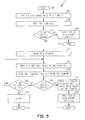
- the adjustment of the long erase pulse in 540may be accomplished with a method 700 shown in FIG. 7 according to an embodiment of the present invention.
- the method 700starts in 702 and determines in 704 whether the counter is less than a low count.
- the low countmay be 3 according to an embodiment of the present invention.
- the long erase pulseis shortened in 706 .
- the long erase pulsemay be shortened by 1 microsecond in 706 according to an embodiment of the present invention.
- the method 700determines in 710 whether the counter is greater than a high count.
- the high countmay be 6 according to an embodiment of the present invention. If the counter is greater than the high count, the long erase pulse is lengthened in 712 .
- the long erase pulsemay be lengthened by 1 microsecond in 712 according to an embodiment of the present invention. If the counter is not greater than the high count the method 700 leaves the long erase pulse unchanged in 720 , and all three branches of the method 700 meet thereafter when the method 700 determines if the long erase pulse is greater than a minimum in 730 . If the long erase pulse is not greater than the minimum, it is set to a minimum length in 732 before the method 700 is done in 740 . The long erase pulse may be set to a minimum length in 732 by adding a variable pulse length that is determined based on the counter to a minimum value according to an embodiment of the present invention. The long erase pulse may also be set to an initial length before the method 700 starts in 702 .
- the adjustment of the long erase pulse in 540may be accomplished with a method 800 shown in FIG. 8 according to another embodiment of the present invention.
- the method 800starts in 802 and calculates a quantity representing short erase pulses applied to the flash cell during several recent erases in 804 .
- the calculation of the quantitymay be done in many ways as will be described hereinbelow.
- the method 800determines in 806 whether the quantity is less than a low limit. If the quantity is less than the low limit, the long erase pulse is shortened in 808 .
- the long erase pulsemay be shortened by one (1) microsecond in 808 according to an embodiment of the present invention. If the quantity is not less than the low limit, the method 800 determines in 810 whether the quantity is greater than a high limit.
- the long erase pulseis lengthened in 812 .
- the long erase pulsemay be lengthened by one (1) microsecond in 812 according to an embodiment of the present invention. If the quantity is not greater than the high limit the method 800 leaves the long erase pulse unchanged in 820 , and all three branches of the method 800 meet thereafter when the method 800 determines if the long erase pulse is greater than a minimum in 830 . If the long erase pulse is not greater than the minimum, it is set to a minimum length in 832 before the method 800 is done in 840 .
- the long erase pulsemay be set to a minimum length in 832 by adding a variable pulse length that is determined based on the quantity to a minimum value according to an embodiment of the present invention.
- the long erase pulsemay also be set to an initial length before the method 800 starts in 802 .
- the calculation of the quantity representing short erase pulses applied to the flash cell during several recent erases in 804may be calculated in several ways according to alternate embodiments of the present invention.
- the quantitymay be calculated by adding a past average of short erase pulses applied to the flash cell prior to the long erase pulse to the counted number of short erase pulses to equal a sum and calculating the quantity as being equal to the sum divided by two.
- the length of the long erase pulsemay be increased if the quantity is more than six (6), and the length of the long erase pulse may be decreased if the quantity of short erase pulses is less than three (3).
- the quantityis an average of short erase pulses applied to the flash cell each time the flash cell is erased, and the average is weighted toward the most recent erase of the flash cell. Equation (1) expresses the calculation where the quantity is represented by Q, the past average is represented by PA, and the counter is represented by K:
- the quantitymay be calculated with a method 900 shown in FIG. 9 according to an embodiment of the present invention.
- the method 900starts in 902 and retrieves a past average from a memory in 904 .
- the past averagerepresents an average of short erase pulses applied in past erases of the flash cell.
- the past averageis added to the counter in 906 to calculate a sum.
- the counterwas incremented in 524 of the method 500 .
- the sumis divided by two (2) in 908 to calculate the quantity, and the quantity is stored as the past average in the memory in 910 before the method 900 is done in 912 .
- the calculation of the quantity representing short erase pulses applied to the flash cell during several recent erases in 804may also be calculated in the following manner according to an embodiment of the present invention.
- the quantitymay be calculated by calculating a sum of short erase pulses applied to the flash cell during eight consecutive erases of the flash cell completed prior to the long erase pulse, and calculating an average by dividing the sum by eight.
- the quantityis then set equal to the sum added to the counted number of short erase pulses, and the average is then subtracted from the quantity to leave the result.
- the length of the long erase pulsemay be increased if the quantity is more than forty eight (48), and the length of the long erase pulse may be decreased if the quantity is less than twenty four (24).
- the quantitymay be calculated with a method 1000 shown in FIG. 10 according to an embodiment of the present invention.
- the method 1000starts in 1002 and retrieves stored counters from past erases from a memory in 1004 .
- a sum of short erase pulses applied to the flash cell during eight consecutive erases of the flash cell completed prior to the long erase pulseis calculated from the stored counters in 1006 .
- the sumis divided by eight (8) in 1008 to calculate an average.
- the quantityis then calculated in 1010 by adding the sum to the counter that was incremented in 524 of the method 500 , and then subtracting the average.
- the method 1000is done in 1012 .
- the calculation of the quantity representing short erase pulses applied to the flash cell during several recent erases in 804may also be calculated in the following manner according to an embodiment of the present invention.
- the quantitymay be calculated by calculating a sum of short erase pulses applied to the flash cell during nine consecutive erases of the flash cell including the most recent erase, and calculating an average by dividing the sum by nine. The quantity is then calculated by subtracting the average from the sum.
- the length of the long erase pulsemay be increased if the quantity is more than forty eight (48), and the length of the long erase pulse may be decreased if the quantity is less than twenty four (24).
- the quantityis an average of short erase pulses applied to the flash cell over eight (8) erases, and the short erase pulses applied during more recent erases are weighted more heavily.
- the quantitymay be calculated with a method 1100 shown in FIG. 11 according to an embodiment of the present invention.
- the method 1100starts in 1102 and retrieves stored counters from past erases from a memory in 1104 .
- a sum of short erase pulses applied to the flash cell during nine consecutive erases of the flash cellis calculated from the counter and the stored counters in 1106 .
- the counterhad been incremented in 524 of the method 500 .
- the sumis divided by nine (9) in 1108 to calculate an average.
- the quantityis then calculated in 1110 by subtracting the average from the sum and the method 1100 is done in 1112 .
- the quantity representing short erase pulses applied to the flash cell during several recent erases calculated as described above and shown with the methods 900 , 1000 , and 1100 shown in FIGS. 9, 10 , and 11is calculated to change the length of the long erase pulse based on the historical trend of all past erases of a flash cell. Recent erases of the flash cell are weighted more heavily than older erases in the calculation of the quantity. The use of the quantity dampens changes in the long erase pulse over time as compared with a calculation based only on the last erase of the flash cell.
- the methods 500 , 700 , 800 , 900 , 1000 , and 1100 of erasing a flash cell according to embodiments of the present inventionwere described herein with reference to a single flash cell, but may be applied to erase multiple flash cells in a block according to alternate embodiments of the present invention.
- the flash cells in a blockare erased together at the same time.
- the length of a long erase pulse 410 applied to erase a flash cellis adjusted based on one or more counts of short erase pulses 412 applied during previous erases of the flash cell.
- the long erase pulse 410was lengthened if too many short erase pulses 412 had been applied in the past, and the long erase pulse 410 was shortened if too few short erase pulses 412 had been applied in the past.
- the length of the long erase pulse 410is variable and is adjusted such that it leaves the flash cell almost or nearly erased, or brings the flash cell to the brink of being erased, each time it is applied during the operating life of the flash cell.
- the long erase pulse 410produces a nearly-erased state in the flash cell consistently even as the flash cell changes physically with age.
- the number of short erase pulses 412 needed to complete the erasing of a flash cellremained within a specified range during the operating life of the flash cell.
- the methods 500 , 700 , 800 , 900 , 1000 , and 1100 described abovehave several advantages in the erasure of a flash cell or a block of flash cells.
- the capability of the long erase pulse 410 to produce a nearly-erased state in the flash cellconsistently reduces the number of times that an erase pulse is applied to the flash cell, and reduces the the number of times that the flash cell will be read to determine if it is erased. This reduces wear on the flash cell and slows its aging process such that it may have a longer operating life.
- short erase pulses 412to gently nudge the flash cell into an erased state reduces the number and frequency of over-erased flash cells because the flash cells are less likely to be pushed into an over-erased state by a single short erase pulse 412 . This reduces the number of heal operations, or the soft programming, used to correct over-erased flash cells, and this reduces wear on the flash cell. Also, the methods 500 , 700 , 800 , 900 , 1000 , and 1100 reduce the time needed to erase one or more flash cells because they reduce the number of times that a flash cell will be read to determine if it is erased, and they reduce the frequency with which the flash cell will be subject to a heal operation or soft programming.
- the methods 500 , 700 , 800 , 900 , 1000 , or 1100may be implemented as a series of programmable instructions stored and implemented in the controller 105 .
- the methods 500 , 700 , 800 , 900 , 1000 , or 1100may also be implemented in the state machine 130 .
- the state machine 130is a sequential logic circuit including both logic gates and storage elements designed to implement algorithms directly in hardware.
- the state machine 130may include logic gates and storage elements to carry out each act of the methods 500 , 700 , 800 , 900 , 1000 , or 1100 .
- Other portions of the IC 110may also be used to implement the methods 500 , 700 , 800 , 900 , 1000 , or 1100 .
- the pump circuit 160may be used to provide any voltages needed to program, erase, or read the flash cell.
- the flash cellmay be read by a sense amplifier in the sense amplifiers 156 , and the read data may be stored in the input data latch 119 .
- the methods 500 , 700 , 800 , 900 , 1000 , or 1100may be implemented in other ways known to those skilled in the art.
- the chip 1200includes an embedded flash memory 1210 such as the flash memory integrated circuit (IC) 110 .
- the embedded flash memory 1210includes elements or instructions to implement the methods 500 , 700 , 800 , 900 , 1000 , or 1100 shown in FIGS. 5, 7 , 8 , 9 , 10 , and 11 and described above according to the embodiments of the present invention.
- the embedded flash memory 1210shares the chip 1200 with another integrated circuit 1220 such as a processor, or possibly several other integrated circuits.
- the embedded flash memory 1210 and the integrated circuit 1220are coupled together by a suitable communication line or bus 1230 .
- FIG. 13a flash memory card 1300 according to an embodiment of the present invention is shown in FIG. 13 .
- the card 1300includes a plurality of flash memory integrated circuits 1310 (1)- 1310 (X) each of which are similar to the flash memory integrated circuit (IC) 110 shown in FIG. 1 .
- the card 1300may be a single integrated circuit in which the flash memory integrated circuits 1310 (1)- 1310 (X) are embedded.
- FIG. 14is a block diagram of an information-handling system 1400 according to an embodiment of the present invention.
- the information-handling system 1400includes a memory system 1408 , a processor 1410 , a display unit 1420 , and an input/output (I/O) subsystem 1430 .
- the processor 1410may be, for example, a microprocessor.
- the memory system 1408is comprised of the flash memory integrated circuit (IC) 110 .
- the memory system 1408includes elements or instructions to implement the methods 500 , 700 , 800 , 900 , 1000 , or 1100 shown in FIGS. 5, 7 , 8 , 9 , 10 , and 11 and described above according to the embodiments of the present invention.
- the I/O subsystem 1430may be a keyboard or other device to allow the user to communicate with the system 1400 .
- the processor 1410 and the memory system 1408may be embedded on a single integrated circuit chip such as the chip 1200 shown in FIG. 12 .
- the processor 1410 , the display unit 1420 , the I/O subsystem 1430 , and the memory system 1408are coupled together by a suitable communication line or bus 1440 .
- the information-handling system 1400is a computer system (such as, for example, a video game, a hand-held calculator, a television set-top box, a fixed-screen telephone, a network computer (NC), a hand-held computer, a personal computer, or a multiprocessor supercomputer), an information appliance (such as, for example, a cellular telephone, a smart mobile phone, a pager, a daily planner or organizer, a personal digital assistant (PDA), or any wireless device), an information component (such as, for example, a magnetic disk drive or telecommunications modem), or other appliance (such as, for example, a television, a hearing aid, washing machine or microwave oven having an electronic controller).
- a computer systemsuch as, for example, a video game, a hand-held calculator, a television set-top box, a fixed-screen telephone, a network computer (NC), a hand-held computer, a personal computer, or a multiprocessor supercomputer
- an information appliancesuch as, for example, a
Landscapes
- Read Only Memory (AREA)
Abstract
Description


Claims (40)
Priority Applications (3)
| Application Number | Priority Date | Filing Date | Title |
|---|---|---|---|
| US09/972,426US6515909B1 (en) | 2001-10-05 | 2001-10-05 | Flash memory device with a variable erase pulse |
| US10/352,603US6903974B2 (en) | 2001-10-05 | 2003-01-28 | Flash memory device with a variable erase pulse |
| US11/085,936US7167399B2 (en) | 2001-10-05 | 2005-03-22 | Flash memory device with a variable erase pulse |
Applications Claiming Priority (1)
| Application Number | Priority Date | Filing Date | Title |
|---|---|---|---|
| US09/972,426US6515909B1 (en) | 2001-10-05 | 2001-10-05 | Flash memory device with a variable erase pulse |
Related Child Applications (1)
| Application Number | Title | Priority Date | Filing Date |
|---|---|---|---|
| US10/352,603ContinuationUS6903974B2 (en) | 2001-10-05 | 2003-01-28 | Flash memory device with a variable erase pulse |
Publications (1)
| Publication Number | Publication Date |
|---|---|
| US6515909B1true US6515909B1 (en) | 2003-02-04 |
Family
ID=25519647
Family Applications (3)
| Application Number | Title | Priority Date | Filing Date |
|---|---|---|---|
| US09/972,426Expired - LifetimeUS6515909B1 (en) | 2001-10-05 | 2001-10-05 | Flash memory device with a variable erase pulse |
| US10/352,603Expired - LifetimeUS6903974B2 (en) | 2001-10-05 | 2003-01-28 | Flash memory device with a variable erase pulse |
| US11/085,936Expired - LifetimeUS7167399B2 (en) | 2001-10-05 | 2005-03-22 | Flash memory device with a variable erase pulse |
Family Applications After (2)
| Application Number | Title | Priority Date | Filing Date |
|---|---|---|---|
| US10/352,603Expired - LifetimeUS6903974B2 (en) | 2001-10-05 | 2003-01-28 | Flash memory device with a variable erase pulse |
| US11/085,936Expired - LifetimeUS7167399B2 (en) | 2001-10-05 | 2005-03-22 | Flash memory device with a variable erase pulse |
Country Status (1)
| Country | Link |
|---|---|
| US (3) | US6515909B1 (en) |
Cited By (36)
| Publication number | Priority date | Publication date | Assignee | Title |
|---|---|---|---|---|
| US20030067809A1 (en)* | 2001-10-09 | 2003-04-10 | Micron Technology, Inc. | Faster method of erasing flash memory |
| US20030090947A1 (en)* | 2000-08-30 | 2003-05-15 | Hitachi, Ltd. | Nonvolatile memory |
| US20030133327A1 (en)* | 2002-01-17 | 2003-07-17 | Mitsubishi Denki Kabushiki Kaisha | Nonvolatile semiconductor storage device having a shortened time required for a data erasing operation and data erasing method thereof |
| US6704233B2 (en)* | 2001-06-12 | 2004-03-09 | Stmicroelectronics, S.R.L. | Sensing circuitry for reading and verifying the contents of electrically programmable and erasable non-volatile memory cells, useful in low supply-voltage technologies |
| US20040184319A1 (en)* | 2002-07-19 | 2004-09-23 | Micron Technology, Inc. | Non-volatile memory erase circuitry |
| US20050024978A1 (en)* | 2003-07-30 | 2005-02-03 | M-Systems Flash Disk Pioneers Ltd. | Method and system for optimizing reliability and performance of programming data in non-volatile memory devices |
| US20060007743A1 (en)* | 2002-05-29 | 2006-01-12 | Micron Technology, Inc. | Flash memory |
| US20060056240A1 (en)* | 2004-04-01 | 2006-03-16 | Saifun Semiconductors, Ltd. | Method, circuit and system for erasing one or more non-volatile memory cells |
| US20070047327A1 (en)* | 2005-08-31 | 2007-03-01 | Micron Technology, Inc. | Erase method for flash memory |
| US20080144396A1 (en)* | 2006-12-19 | 2008-06-19 | Kuo-Tung Chang | Erasing flash memory using adaptive drain and/or gate bias |
| DE102007062674A1 (en)* | 2007-12-12 | 2009-06-18 | Qimonda Flash Gmbh | Integrated circuits, memory control unit and memory modules |
| US20100208523A1 (en)* | 2009-02-13 | 2010-08-19 | Micron Technology, Inc. | Dynamic soft program trims |
| US20100332729A1 (en)* | 2009-06-30 | 2010-12-30 | Sandisk Il Ltd. | Memory operations using location-based parameters |
| US20110035536A1 (en)* | 2009-08-06 | 2011-02-10 | Samsung Electronics Co., Ltd. | Non-volatile memory device generating wear-leveling information and method of operating the same |
| EP2286412A1 (en)* | 2007-12-21 | 2011-02-23 | Rambus Inc. | Flash memory timing pre-characterization for use in ormal operation |
| US20110103150A1 (en)* | 2009-11-02 | 2011-05-05 | Infineon Technologies Ag | Non-volatile memory with predictive programming |
| EP2487688A3 (en)* | 2011-02-09 | 2012-10-31 | Freescale Semiconductor, Inc. Are | Erase ramp pulse width control for non-volatile memory |
| US8972627B2 (en) | 2009-09-09 | 2015-03-03 | Fusion-Io, Inc. | Apparatus, system, and method for managing operations for data storage media |
| US8984216B2 (en) | 2010-09-09 | 2015-03-17 | Fusion-Io, Llc | Apparatus, system, and method for managing lifetime of a storage device |
| US9021158B2 (en) | 2009-09-09 | 2015-04-28 | SanDisk Technologies, Inc. | Program suspend/resume for memory |
| US9152555B2 (en) | 2013-11-15 | 2015-10-06 | Sandisk Enterprise IP LLC. | Data management with modular erase in a data storage system |
| US9218278B2 (en) | 2010-12-13 | 2015-12-22 | SanDisk Technologies, Inc. | Auto-commit memory |
| US9223514B2 (en) | 2009-09-09 | 2015-12-29 | SanDisk Technologies, Inc. | Erase suspend/resume for memory |
| US9305610B2 (en) | 2009-09-09 | 2016-04-05 | SanDisk Technologies, Inc. | Apparatus, system, and method for power reduction management in a storage device |
| US9384844B1 (en) | 2015-07-03 | 2016-07-05 | Powerchip Technology Corporation | Flash memory apparatus and data erasing method thereof |
| US9600184B2 (en) | 2007-12-06 | 2017-03-21 | Sandisk Technologies Llc | Apparatus, system, and method for coordinating storage requests in a multi-processor/multi-thread environment |
| US9666244B2 (en) | 2014-03-01 | 2017-05-30 | Fusion-Io, Inc. | Dividing a storage procedure |
| US9734086B2 (en) | 2006-12-06 | 2017-08-15 | Sandisk Technologies Llc | Apparatus, system, and method for a device shared between multiple independent hosts |
| US9767017B2 (en) | 2010-12-13 | 2017-09-19 | Sandisk Technologies Llc | Memory device with volatile and non-volatile media |
| US20170337974A1 (en)* | 2008-01-25 | 2017-11-23 | Micron Technology, Inc. | Random telegraph signal noise reduction scheme for semiconductor memories |
| US9933950B2 (en) | 2015-01-16 | 2018-04-03 | Sandisk Technologies Llc | Storage operation interrupt |
| US20180373437A1 (en)* | 2017-06-26 | 2018-12-27 | Western Digital Technologies, Inc. | Adaptive system for optimization of non-volatile storage operational parameters |
| US10379769B2 (en)* | 2016-12-30 | 2019-08-13 | Western Digital Technologies, Inc. | Continuous adaptive calibration for flash memory devices |
| CN110895449A (en)* | 2018-09-12 | 2020-03-20 | 爱思开海力士有限公司 | Apparatus and method for managing valid data in a memory system |
| US10817502B2 (en) | 2010-12-13 | 2020-10-27 | Sandisk Technologies Llc | Persistent memory management |
| US10817421B2 (en) | 2010-12-13 | 2020-10-27 | Sandisk Technologies Llc | Persistent data structures |
Families Citing this family (43)
| Publication number | Priority date | Publication date | Assignee | Title |
|---|---|---|---|---|
| US7158559B2 (en) | 2002-01-15 | 2007-01-02 | Tensor Comm, Inc. | Serial cancellation receiver design for a coded signal processing engine |
| US8085889B1 (en) | 2005-04-11 | 2011-12-27 | Rambus Inc. | Methods for managing alignment and latency in interference cancellation |
| US6515909B1 (en)* | 2001-10-05 | 2003-02-04 | Micron Technology Inc. | Flash memory device with a variable erase pulse |
| TWI259952B (en)* | 2002-01-31 | 2006-08-11 | Macronix Int Co Ltd | Data erase method of flash memory |
| JP4262033B2 (en)* | 2003-08-27 | 2009-05-13 | 株式会社ルネサステクノロジ | Semiconductor integrated circuit |
| US6975538B2 (en)* | 2003-10-08 | 2005-12-13 | Micron Technology, Inc. | Memory block erasing in a flash memory device |
| US7203109B1 (en)* | 2005-12-21 | 2007-04-10 | Motorola, Inc. | Device and method for detecting corruption of digital hardware configuration |
| US7916543B2 (en)* | 2007-10-22 | 2011-03-29 | Micron Technology, Inc. | Memory cell operation |
| US9074193B2 (en)* | 2008-04-09 | 2015-07-07 | University Of Florida Research Foundation, Inc. | Heat resistant plants and plant tissues and methods and materials for making and using same |
| WO2009134044A2 (en)* | 2008-04-29 | 2009-11-05 | Lg Electronics Inc. | Home appliance and home appliance system |
| US8532273B2 (en) | 2008-04-29 | 2013-09-10 | Lg Electronics Inc. | Home appliance and home appliance system |
| KR101627219B1 (en)* | 2008-04-29 | 2016-06-03 | 엘지전자 주식회사 | Home appliance and home appliance system |
| US8705715B2 (en)* | 2008-04-30 | 2014-04-22 | Lg Electronics Inc. | Home appliance, home appliance system, and diagnosis method of a home appliance |
| US20100040213A1 (en)* | 2008-04-30 | 2010-02-18 | Lg Electronics Inc. | Home appliance and home appliance system |
| US8031521B1 (en)* | 2008-05-20 | 2011-10-04 | Marvell International Ltd. | Reprogramming non-volatile memory devices for read disturbance mitigation |
| KR100953045B1 (en)* | 2008-05-23 | 2010-04-14 | 주식회사 하이닉스반도체 | How to Program Nonvolatile Memory Devices |
| US9054953B2 (en)* | 2008-06-16 | 2015-06-09 | Lg Electronics Inc. | Home appliance and home appliance system |
| US20100066554A1 (en)* | 2008-09-02 | 2010-03-18 | Lg Electronics Inc. | Home appliance system |
| KR20100112948A (en)* | 2009-04-10 | 2010-10-20 | 엘지전자 주식회사 | Diagnostic system and method for home appliance |
| KR101597523B1 (en)* | 2009-04-10 | 2016-02-25 | 엘지전자 주식회사 | Home appliance service device and control method thereof |
| US8565079B2 (en)* | 2009-04-10 | 2013-10-22 | Lg Electronics Inc. | Home appliance and home appliance system |
| KR101421685B1 (en)* | 2009-04-10 | 2014-08-13 | 엘지전자 주식회사 | Home appliance diagnosis system and its diagnosis method |
| KR101442115B1 (en) | 2009-04-10 | 2014-09-18 | 엘지전자 주식회사 | Home Appliances & Home Appliances System |
| EP2453610B1 (en) | 2009-07-06 | 2019-05-15 | LG Electronics Inc. | Home appliance diagnosis system, and method for operating same |
| KR20110010374A (en)* | 2009-07-24 | 2011-02-01 | 엘지전자 주식회사 | Home appliance diagnostic system and method |
| KR101482138B1 (en)* | 2009-07-31 | 2015-01-13 | 엘지전자 주식회사 | Home appliance diagnosis system and its diagnosis method |
| KR101472402B1 (en)* | 2009-07-31 | 2014-12-12 | 엘지전자 주식회사 | Home appliance diagnosis system and its diagnosis method |
| KR101553843B1 (en)* | 2009-07-31 | 2015-09-30 | 엘지전자 주식회사 | Diagnostic system and method for home appliance |
| KR101472401B1 (en)* | 2009-07-31 | 2014-12-12 | 엘지전자 주식회사 | Home appliance diagnosis system and its diagnosis method |
| KR20110013582A (en)* | 2009-07-31 | 2011-02-10 | 엘지전자 주식회사 | Home appliance diagnostic system and diagnosis method |
| RU2495471C1 (en)* | 2009-08-05 | 2013-10-10 | ЭлДжи ЭЛЕКТРОНИКС ИНК. | Household appliance and method of its operation |
| US8479061B2 (en)* | 2009-09-24 | 2013-07-02 | AGIGA Tech | Solid state memory cartridge with wear indication |
| KR101748605B1 (en) | 2010-01-15 | 2017-06-20 | 엘지전자 주식회사 | Refrigerator and diagnostic system for the refrigerator |
| US10325269B2 (en) | 2010-07-06 | 2019-06-18 | Lg Electronics Inc. | Home appliance diagnosis system and diagnosis method for same |
| US8737138B2 (en)* | 2010-11-18 | 2014-05-27 | Micron Technology, Inc. | Memory instruction including parameter to affect operating condition of memory |
| KR101416937B1 (en) | 2011-08-02 | 2014-08-06 | 엘지전자 주식회사 | home appliance, home appliance diagnostic system, and method |
| KR101252167B1 (en) | 2011-08-18 | 2013-04-05 | 엘지전자 주식회사 | Diagnostic system and method for home appliance |
| US8627158B2 (en)* | 2011-12-08 | 2014-01-07 | International Business Machines Corporation | Flash array built in self test engine with trace array and flash metric reporting |
| US8862952B1 (en)* | 2012-03-16 | 2014-10-14 | Western Digital Technologies, Inc. | Prioritized memory scanning for data storage systems |
| US8724388B2 (en)* | 2012-04-02 | 2014-05-13 | Spansion Llc | Adaptively programming or erasing flash memory blocks |
| KR101942781B1 (en) | 2012-07-03 | 2019-01-28 | 엘지전자 주식회사 | Home appliance and method of outputting audible signal for diagnosis |
| KR20140007178A (en) | 2012-07-09 | 2014-01-17 | 엘지전자 주식회사 | Diagnostic system for home appliance |
| US9728278B2 (en) | 2014-10-24 | 2017-08-08 | Micron Technology, Inc. | Threshold voltage margin analysis |
Citations (10)
| Publication number | Priority date | Publication date | Assignee | Title |
|---|---|---|---|---|
| US5636166A (en) | 1995-12-05 | 1997-06-03 | Micron Quantum Devices, Inc. | Apparatus for externally timing high voltage cycles of non-volatile memory system |
| US5680350A (en) | 1994-12-14 | 1997-10-21 | Micron Technology, Inc. | Method for narrowing threshold voltage distribution in a block erased flash memory array |
| US5784316A (en)* | 1995-11-24 | 1998-07-21 | Nec Corporation | Non-volatile storage device |
| US5801985A (en) | 1995-07-28 | 1998-09-01 | Micron Technology, Inc. | Memory system having programmable control parameters |
| US5901194A (en) | 1995-07-28 | 1999-05-04 | Micron Technologies, Inc | Timer circuit with programmable decode circuitry |
| US6020775A (en)* | 1995-07-28 | 2000-02-01 | Micron Technology, Inc. | Adjustable timer circuit |
| US6115291A (en)* | 1998-12-29 | 2000-09-05 | Micron Technology, Inc. | Healing cells in a memory device |
| US6188613B1 (en) | 1998-10-08 | 2001-02-13 | Micron Technology, Inc. | Device and method in a semiconductor memory for erasing/programming memory cells using erase/program speeds stored for each cell |
| US6248629B1 (en)* | 1998-03-18 | 2001-06-19 | Advanced Micro Devices, Inc. | Process for fabricating a flash memory device |
| US6356974B2 (en) | 1995-07-28 | 2002-03-12 | Micron Technology, Inc. | Architecture for state machine for controlling internal operations of flash memory |
Family Cites Families (4)
| Publication number | Priority date | Publication date | Assignee | Title |
|---|---|---|---|---|
| US5268319A (en)* | 1988-06-08 | 1993-12-07 | Eliyahou Harari | Highly compact EPROM and flash EEPROM devices |
| US5822252A (en)* | 1996-03-29 | 1998-10-13 | Aplus Integrated Circuits, Inc. | Flash memory wordline decoder with overerase repair |
| US6148435A (en)* | 1997-12-24 | 2000-11-14 | Cypress Semiconductor Corporation | Optimized programming/erase parameters for programmable devices |
| US6515909B1 (en)* | 2001-10-05 | 2003-02-04 | Micron Technology Inc. | Flash memory device with a variable erase pulse |
- 2001
- 2001-10-05USUS09/972,426patent/US6515909B1/ennot_activeExpired - Lifetime
- 2003
- 2003-01-28USUS10/352,603patent/US6903974B2/ennot_activeExpired - Lifetime
- 2005
- 2005-03-22USUS11/085,936patent/US7167399B2/ennot_activeExpired - Lifetime
Patent Citations (13)
| Publication number | Priority date | Publication date | Assignee | Title |
|---|---|---|---|---|
| US5680350A (en) | 1994-12-14 | 1997-10-21 | Micron Technology, Inc. | Method for narrowing threshold voltage distribution in a block erased flash memory array |
| US6020775A (en)* | 1995-07-28 | 2000-02-01 | Micron Technology, Inc. | Adjustable timer circuit |
| US5801985A (en) | 1995-07-28 | 1998-09-01 | Micron Technology, Inc. | Memory system having programmable control parameters |
| US5901194A (en) | 1995-07-28 | 1999-05-04 | Micron Technologies, Inc | Timer circuit with programmable decode circuitry |
| US6081575A (en) | 1995-07-28 | 2000-06-27 | Micron Technology, Inc. | Timer circuit with programmable decode circuitry |
| US6272586B1 (en) | 1995-07-28 | 2001-08-07 | Micron Technology, Inc. | Memory system having programmable control parameters |
| US6356974B2 (en) | 1995-07-28 | 2002-03-12 | Micron Technology, Inc. | Architecture for state machine for controlling internal operations of flash memory |
| US5784316A (en)* | 1995-11-24 | 1998-07-21 | Nec Corporation | Non-volatile storage device |
| US5901108A (en) | 1995-12-05 | 1999-05-04 | Micron Technology, Inc. | Apparatus for externally timing high voltage cycles of non-volatile memory system |
| US5636166A (en) | 1995-12-05 | 1997-06-03 | Micron Quantum Devices, Inc. | Apparatus for externally timing high voltage cycles of non-volatile memory system |
| US6248629B1 (en)* | 1998-03-18 | 2001-06-19 | Advanced Micro Devices, Inc. | Process for fabricating a flash memory device |
| US6188613B1 (en) | 1998-10-08 | 2001-02-13 | Micron Technology, Inc. | Device and method in a semiconductor memory for erasing/programming memory cells using erase/program speeds stored for each cell |
| US6115291A (en)* | 1998-12-29 | 2000-09-05 | Micron Technology, Inc. | Healing cells in a memory device |
Cited By (87)
| Publication number | Priority date | Publication date | Assignee | Title |
|---|---|---|---|---|
| US7317640B2 (en) | 2000-08-30 | 2008-01-08 | Renesas Technology Corp. | Nonvolatile memory with erasable parts |
| US20030090947A1 (en)* | 2000-08-30 | 2003-05-15 | Hitachi, Ltd. | Nonvolatile memory |
| US20060279995A1 (en)* | 2000-08-30 | 2006-12-14 | Renesas Technology Corp. | Nonvolatile memory |
| US7130218B2 (en) | 2000-08-30 | 2006-10-31 | Renesas Technology Corp. | Nonvolatile memory with controlled voltage boosting speed |
| US6791884B2 (en)* | 2000-08-30 | 2004-09-14 | Renesas Technology Corp. | Nonvolatile memory |
| US20050157556A1 (en)* | 2000-08-30 | 2005-07-21 | Renesas Technology Corp. | Nonvolatile memory |
| US6704233B2 (en)* | 2001-06-12 | 2004-03-09 | Stmicroelectronics, S.R.L. | Sensing circuitry for reading and verifying the contents of electrically programmable and erasable non-volatile memory cells, useful in low supply-voltage technologies |
| US20040057291A1 (en)* | 2001-06-12 | 2004-03-25 | Stmicroelectronics S.R.L. | Sensing circuitry for reading and verifying the contents of electrically programmable and erasable non-volatile memory cells, useful in low supply-voltage technologies |
| US6906957B2 (en) | 2001-06-12 | 2005-06-14 | Stmicroelectronics S.R.L. | Sensing circuitry for reading and verifying the contents of electrically programmable and erasable non-volatile memory cells, useful in low supply-voltage technologies |
| US20070223285A1 (en)* | 2001-10-09 | 2007-09-27 | Micron Technology, Inc. | Method of erasing flash memory |
| US7554852B2 (en) | 2001-10-09 | 2009-06-30 | Micron Technology, Inc. | Method of erasing flash memory with pre-programming memory cells only in the presence of a cell leakage |
| US20030067809A1 (en)* | 2001-10-09 | 2003-04-10 | Micron Technology, Inc. | Faster method of erasing flash memory |
| US20060004960A1 (en)* | 2001-10-09 | 2006-01-05 | Micron Technology, Inc. | Faster method of erasing flash memory |
| US20060002194A1 (en)* | 2001-10-09 | 2006-01-05 | Micron Technology, Inc. | Faster method of erasing flash memory |
| US7233525B2 (en) | 2001-10-09 | 2007-06-19 | Micron Technology, Inc. | Method of converting contents of flash memory cells in the presence of leakage |
| US7061811B2 (en) | 2001-10-09 | 2006-06-13 | Micron Technology, Inc. | Faster method of erasing flash memory |
| US7061810B2 (en) | 2001-10-09 | 2006-06-13 | Micron Technology, Inc. | Erasing flash memory without pre-programming the flash memory before erasing |
| US6781882B2 (en)* | 2002-01-17 | 2004-08-24 | Renesas Technology Corp. | Nonvolatile semiconductor storage device having a shortened time required for a data erasing operation and data erasing method thereof |
| US20030133327A1 (en)* | 2002-01-17 | 2003-07-17 | Mitsubishi Denki Kabushiki Kaisha | Nonvolatile semiconductor storage device having a shortened time required for a data erasing operation and data erasing method thereof |
| US20060007743A1 (en)* | 2002-05-29 | 2006-01-12 | Micron Technology, Inc. | Flash memory |
| US7068543B2 (en)* | 2002-05-29 | 2006-06-27 | Micron Technology, Inc. | Flash memory |
| US6876583B2 (en)* | 2002-07-19 | 2005-04-05 | Micron Technology, Inc. | Non-volatile memory erase circuitry |
| US20040184319A1 (en)* | 2002-07-19 | 2004-09-23 | Micron Technology, Inc. | Non-volatile memory erase circuitry |
| US20050024978A1 (en)* | 2003-07-30 | 2005-02-03 | M-Systems Flash Disk Pioneers Ltd. | Method and system for optimizing reliability and performance of programming data in non-volatile memory devices |
| US7437498B2 (en)* | 2003-07-30 | 2008-10-14 | San Disk Il, Ltd | Method and system for optimizing reliability and performance of programming data in non-volatile memory devices |
| WO2005094178A3 (en)* | 2004-04-01 | 2007-01-04 | Saifun Semiconductors Ltd | Method, circuit and systems for erasing one or more non-volatile memory cells |
| US20060056240A1 (en)* | 2004-04-01 | 2006-03-16 | Saifun Semiconductors, Ltd. | Method, circuit and system for erasing one or more non-volatile memory cells |
| US7652930B2 (en)* | 2004-04-01 | 2010-01-26 | Saifun Semiconductors Ltd. | Method, circuit and system for erasing one or more non-volatile memory cells |
| US20070047327A1 (en)* | 2005-08-31 | 2007-03-01 | Micron Technology, Inc. | Erase method for flash memory |
| US11573909B2 (en) | 2006-12-06 | 2023-02-07 | Unification Technologies Llc | Apparatus, system, and method for managing commands of solid-state storage using bank interleave |
| US11847066B2 (en) | 2006-12-06 | 2023-12-19 | Unification Technologies Llc | Apparatus, system, and method for managing commands of solid-state storage using bank interleave |
| US11640359B2 (en) | 2006-12-06 | 2023-05-02 | Unification Technologies Llc | Systems and methods for identifying storage resources that are not in use |
| US11960412B2 (en) | 2006-12-06 | 2024-04-16 | Unification Technologies Llc | Systems and methods for identifying storage resources that are not in use |
| US9734086B2 (en) | 2006-12-06 | 2017-08-15 | Sandisk Technologies Llc | Apparatus, system, and method for a device shared between multiple independent hosts |
| US7778088B2 (en)* | 2006-12-19 | 2010-08-17 | Spansion Llc | Erasing flash memory using adaptive drain and/or gate bias |
| US20080144396A1 (en)* | 2006-12-19 | 2008-06-19 | Kuo-Tung Chang | Erasing flash memory using adaptive drain and/or gate bias |
| US20100265775A1 (en)* | 2006-12-19 | 2010-10-21 | Kuo-Tung Chang | Erasing flash memory using adaptive drain and/or gate bias |
| US8144522B2 (en) | 2006-12-19 | 2012-03-27 | Spansion Llc | Erasing flash memory using adaptive drain and/or gate bias |
| US9600184B2 (en) | 2007-12-06 | 2017-03-21 | Sandisk Technologies Llc | Apparatus, system, and method for coordinating storage requests in a multi-processor/multi-thread environment |
| US20090154264A1 (en)* | 2007-12-12 | 2009-06-18 | Andreas Kux | Integrated circuits, memory controller, and memory modules |
| DE102007062674A1 (en)* | 2007-12-12 | 2009-06-18 | Qimonda Flash Gmbh | Integrated circuits, memory control unit and memory modules |
| US7636258B2 (en) | 2007-12-12 | 2009-12-22 | Qimonda Flash Gmbh | Integrated circuits, memory controller, and memory modules |
| EP2286412A1 (en)* | 2007-12-21 | 2011-02-23 | Rambus Inc. | Flash memory timing pre-characterization for use in ormal operation |
| US8990485B2 (en) | 2007-12-21 | 2015-03-24 | Rambus Inc. | Memory pre-characterization |
| US9934866B2 (en) | 2007-12-21 | 2018-04-03 | Rambus Inc. | Memory device with defined programming transaction time |
| US20110191526A1 (en)* | 2007-12-21 | 2011-08-04 | Brent Haukness | Flash Memory Timing Pre-Characterization |
| US8484407B2 (en) | 2007-12-21 | 2013-07-09 | Rambus Inc. | Flash memory timing pre-characterization |
| US11462277B2 (en) | 2008-01-25 | 2022-10-04 | Micron Technology, Inc. | Random telegraph signal noise reduction scheme for semiconductor memories |
| US10510420B2 (en) | 2008-01-25 | 2019-12-17 | Micron Technology, Inc. | Random telegraph signal noise reduction scheme for semiconductor memories |
| US10102914B2 (en)* | 2008-01-25 | 2018-10-16 | Micron Technology, Inc. | Random telegraph signal noise reduction scheme for semiconductor memories |
| US11887675B2 (en) | 2008-01-25 | 2024-01-30 | Micron Technology, Inc. | Random telegraph signal noise reduction scheme for semiconductor memories |
| US20170337974A1 (en)* | 2008-01-25 | 2017-11-23 | Micron Technology, Inc. | Random telegraph signal noise reduction scheme for semiconductor memories |
| US10998054B2 (en) | 2008-01-25 | 2021-05-04 | Micron Technology, Inc. | Random telegraph signal noise reduction scheme for semiconductor memories |
| US20100208523A1 (en)* | 2009-02-13 | 2010-08-19 | Micron Technology, Inc. | Dynamic soft program trims |
| US20110182122A1 (en)* | 2009-02-13 | 2011-07-28 | Micron Technology, Inc. | Dynamic soft program trims |
| US7920427B2 (en) | 2009-02-13 | 2011-04-05 | Micron Technology, Inc. | Dynamic soft program trims |
| US8199585B2 (en) | 2009-02-13 | 2012-06-12 | Micron Technology, Inc. | Dynamic soft program trims |
| US8874825B2 (en) | 2009-06-30 | 2014-10-28 | Sandisk Technologies Inc. | Storage device and method using parameters based on physical memory block location |
| US20100332729A1 (en)* | 2009-06-30 | 2010-12-30 | Sandisk Il Ltd. | Memory operations using location-based parameters |
| US9141524B2 (en) | 2009-06-30 | 2015-09-22 | Sandisk Technologies Inc. | Storage device and method including accessing a word line of a memory using parameters selected according to groups of word lines |
| US20110035536A1 (en)* | 2009-08-06 | 2011-02-10 | Samsung Electronics Co., Ltd. | Non-volatile memory device generating wear-leveling information and method of operating the same |
| US9223514B2 (en) | 2009-09-09 | 2015-12-29 | SanDisk Technologies, Inc. | Erase suspend/resume for memory |
| US9021158B2 (en) | 2009-09-09 | 2015-04-28 | SanDisk Technologies, Inc. | Program suspend/resume for memory |
| US9305610B2 (en) | 2009-09-09 | 2016-04-05 | SanDisk Technologies, Inc. | Apparatus, system, and method for power reduction management in a storage device |
| US8972627B2 (en) | 2009-09-09 | 2015-03-03 | Fusion-Io, Inc. | Apparatus, system, and method for managing operations for data storage media |
| US20110103150A1 (en)* | 2009-11-02 | 2011-05-05 | Infineon Technologies Ag | Non-volatile memory with predictive programming |
| US8243520B2 (en) | 2009-11-02 | 2012-08-14 | Infineon Technologies Ag | Non-volatile memory with predictive programming |
| US8984216B2 (en) | 2010-09-09 | 2015-03-17 | Fusion-Io, Llc | Apparatus, system, and method for managing lifetime of a storage device |
| US9767017B2 (en) | 2010-12-13 | 2017-09-19 | Sandisk Technologies Llc | Memory device with volatile and non-volatile media |
| US9772938B2 (en) | 2010-12-13 | 2017-09-26 | Sandisk Technologies Llc | Auto-commit memory metadata and resetting the metadata by writing to special address in free space of page storing the metadata |
| US9218278B2 (en) | 2010-12-13 | 2015-12-22 | SanDisk Technologies, Inc. | Auto-commit memory |
| US10817502B2 (en) | 2010-12-13 | 2020-10-27 | Sandisk Technologies Llc | Persistent memory management |
| US10817421B2 (en) | 2010-12-13 | 2020-10-27 | Sandisk Technologies Llc | Persistent data structures |
| US8345485B2 (en) | 2011-02-09 | 2013-01-01 | Freescale Semiconductor, Inc. | Erase ramp pulse width control for non-volatile memory |
| EP2487688A3 (en)* | 2011-02-09 | 2012-10-31 | Freescale Semiconductor, Inc. Are | Erase ramp pulse width control for non-volatile memory |
| US9152555B2 (en) | 2013-11-15 | 2015-10-06 | Sandisk Enterprise IP LLC. | Data management with modular erase in a data storage system |
| US9666244B2 (en) | 2014-03-01 | 2017-05-30 | Fusion-Io, Inc. | Dividing a storage procedure |
| US9933950B2 (en) | 2015-01-16 | 2018-04-03 | Sandisk Technologies Llc | Storage operation interrupt |
| CN106328202B (en)* | 2015-07-03 | 2020-02-07 | 力晶积成电子制造股份有限公司 | Flash memory device and data erasing method |
| TWI571879B (en)* | 2015-07-03 | 2017-02-21 | 力晶科技股份有限公司 | Flash memory apparatus and data erasing method thereof |
| CN106328202A (en)* | 2015-07-03 | 2017-01-11 | 力晶科技股份有限公司 | Flash memory device and data erasing method |
| US9384844B1 (en) | 2015-07-03 | 2016-07-05 | Powerchip Technology Corporation | Flash memory apparatus and data erasing method thereof |
| US10379769B2 (en)* | 2016-12-30 | 2019-08-13 | Western Digital Technologies, Inc. | Continuous adaptive calibration for flash memory devices |
| US10891052B2 (en)* | 2017-06-26 | 2021-01-12 | Western Digital Technologies, Inc. | Adaptive system for optimization of non-volatile storage operational parameters |
| US20180373437A1 (en)* | 2017-06-26 | 2018-12-27 | Western Digital Technologies, Inc. | Adaptive system for optimization of non-volatile storage operational parameters |
| CN110895449A (en)* | 2018-09-12 | 2020-03-20 | 爱思开海力士有限公司 | Apparatus and method for managing valid data in a memory system |
| CN110895449B (en)* | 2018-09-12 | 2023-07-25 | 爱思开海力士有限公司 | Apparatus and method for managing valid data in a memory system |
Also Published As
| Publication number | Publication date |
|---|---|
| US20030112671A1 (en) | 2003-06-19 |
| US7167399B2 (en) | 2007-01-23 |
| US20050162909A1 (en) | 2005-07-28 |
| US6903974B2 (en) | 2005-06-07 |
Similar Documents
| Publication | Publication Date | Title |
|---|---|---|
| US6515909B1 (en) | Flash memory device with a variable erase pulse | |
| US6650585B2 (en) | Leakage detection in programming algorithm for a flash memory device | |
| US6996004B1 (en) | Minimization of FG-FG coupling in flash memory | |
| US6584019B1 (en) | Leakage detection in flash memory cell | |
| US7092294B2 (en) | Nonvolatile semiconductor memory | |
| US6785162B2 (en) | Test mode decoder in a flash memory | |
| US6549462B1 (en) | Memory cell of nonvolatile semiconductor memory device | |
| US7554852B2 (en) | Method of erasing flash memory with pre-programming memory cells only in the presence of a cell leakage | |
| EP0762429B1 (en) | Method of programming a flash EEPROM memory cell optimized for low power consumption and a method for erasing said cell | |
| US6813183B2 (en) | Externally triggered leakage detection and repair in a flash memory device | |
| US10347340B2 (en) | Memory array and method for reading, programming and erasing the same | |
| US6990022B2 (en) | Semiconductor memory device and portable electronic apparatus | |
| US6441428B1 (en) | One-sided floating-gate memory cell | |
| US7009884B2 (en) | Semiconductor storage device, display device and portable electronic equipment | |
| JP4049641B2 (en) | Nonvolatile semiconductor memory device | |
| WO1996019810A1 (en) | Method for tightening vt distribution of 5 volt-only flash eeproms | |
| US7170791B2 (en) | Programming verification method of nonvolatile memory cell, semiconductor memory device, and portable electronic apparatus having the semiconductor memory device | |
| US6188613B1 (en) | Device and method in a semiconductor memory for erasing/programming memory cells using erase/program speeds stored for each cell | |
| US6545913B2 (en) | Memory cell of nonvolatile semiconductor memory device | |
| JP2005332502A (en) | Semiconductor device and ic card |
Legal Events
| Date | Code | Title | Description |
|---|---|---|---|
| AS | Assignment | Owner name:MICRON TECHNOLOGY, INC., IDAHO Free format text:ASSIGNMENT OF ASSIGNORS INTEREST;ASSIGNOR:WOOLDRIDGE, CORLEY B.;REEL/FRAME:012240/0068 Effective date:20010928 | |
| STCF | Information on status: patent grant | Free format text:PATENTED CASE | |
| FPAY | Fee payment | Year of fee payment:4 | |
| FPAY | Fee payment | Year of fee payment:8 | |
| FPAY | Fee payment | Year of fee payment:12 | |
| AS | Assignment | Owner name:U.S. BANK NATIONAL ASSOCIATION, AS COLLATERAL AGENT, CALIFORNIA Free format text:SECURITY INTEREST;ASSIGNOR:MICRON TECHNOLOGY, INC.;REEL/FRAME:038669/0001 Effective date:20160426 Owner name:U.S. BANK NATIONAL ASSOCIATION, AS COLLATERAL AGEN Free format text:SECURITY INTEREST;ASSIGNOR:MICRON TECHNOLOGY, INC.;REEL/FRAME:038669/0001 Effective date:20160426 | |
| AS | Assignment | Owner name:MORGAN STANLEY SENIOR FUNDING, INC., AS COLLATERAL AGENT, MARYLAND Free format text:PATENT SECURITY AGREEMENT;ASSIGNOR:MICRON TECHNOLOGY, INC.;REEL/FRAME:038954/0001 Effective date:20160426 Owner name:MORGAN STANLEY SENIOR FUNDING, INC., AS COLLATERAL Free format text:PATENT SECURITY AGREEMENT;ASSIGNOR:MICRON TECHNOLOGY, INC.;REEL/FRAME:038954/0001 Effective date:20160426 | |
| AS | Assignment | Owner name:U.S. BANK NATIONAL ASSOCIATION, AS COLLATERAL AGENT, CALIFORNIA Free format text:CORRECTIVE ASSIGNMENT TO CORRECT THE REPLACE ERRONEOUSLY FILED PATENT #7358718 WITH THE CORRECT PATENT #7358178 PREVIOUSLY RECORDED ON REEL 038669 FRAME 0001. ASSIGNOR(S) HEREBY CONFIRMS THE SECURITY INTEREST;ASSIGNOR:MICRON TECHNOLOGY, INC.;REEL/FRAME:043079/0001 Effective date:20160426 Owner name:U.S. BANK NATIONAL ASSOCIATION, AS COLLATERAL AGEN Free format text:CORRECTIVE ASSIGNMENT TO CORRECT THE REPLACE ERRONEOUSLY FILED PATENT #7358718 WITH THE CORRECT PATENT #7358178 PREVIOUSLY RECORDED ON REEL 038669 FRAME 0001. ASSIGNOR(S) HEREBY CONFIRMS THE SECURITY INTEREST;ASSIGNOR:MICRON TECHNOLOGY, INC.;REEL/FRAME:043079/0001 Effective date:20160426 | |
| AS | Assignment | Owner name:JPMORGAN CHASE BANK, N.A., AS COLLATERAL AGENT, ILLINOIS Free format text:SECURITY INTEREST;ASSIGNORS:MICRON TECHNOLOGY, INC.;MICRON SEMICONDUCTOR PRODUCTS, INC.;REEL/FRAME:047540/0001 Effective date:20180703 Owner name:JPMORGAN CHASE BANK, N.A., AS COLLATERAL AGENT, IL Free format text:SECURITY INTEREST;ASSIGNORS:MICRON TECHNOLOGY, INC.;MICRON SEMICONDUCTOR PRODUCTS, INC.;REEL/FRAME:047540/0001 Effective date:20180703 | |
| AS | Assignment | Owner name:MICRON TECHNOLOGY, INC., IDAHO Free format text:RELEASE BY SECURED PARTY;ASSIGNOR:U.S. BANK NATIONAL ASSOCIATION, AS COLLATERAL AGENT;REEL/FRAME:047243/0001 Effective date:20180629 | |
| AS | Assignment | Owner name:MICRON TECHNOLOGY, INC., IDAHO Free format text:RELEASE BY SECURED PARTY;ASSIGNOR:MORGAN STANLEY SENIOR FUNDING, INC., AS COLLATERAL AGENT;REEL/FRAME:050937/0001 Effective date:20190731 | |
| AS | Assignment | Owner name:MICRON TECHNOLOGY, INC., IDAHO Free format text:RELEASE BY SECURED PARTY;ASSIGNOR:JPMORGAN CHASE BANK, N.A., AS COLLATERAL AGENT;REEL/FRAME:051028/0001 Effective date:20190731 Owner name:MICRON SEMICONDUCTOR PRODUCTS, INC., IDAHO Free format text:RELEASE BY SECURED PARTY;ASSIGNOR:JPMORGAN CHASE BANK, N.A., AS COLLATERAL AGENT;REEL/FRAME:051028/0001 Effective date:20190731 |